US6346763B1 - High output stacked piezoelectric transformer - Google Patents
High output stacked piezoelectric transformer Download PDFInfo
- Publication number
- US6346763B1 US6346763B1 US09/602,510 US60251000A US6346763B1 US 6346763 B1 US6346763 B1 US 6346763B1 US 60251000 A US60251000 A US 60251000A US 6346763 B1 US6346763 B1 US 6346763B1
- Authority
- US
- United States
- Prior art keywords
- electrode
- ine
- piezoelectric element
- input
- oute
- Prior art date
- Legal status (The legal status is an assumption and is not a legal conclusion. Google has not performed a legal analysis and makes no representation as to the accuracy of the status listed.)
- Expired - Fee Related
Links
- 230000010355 oscillation Effects 0.000 abstract description 12
- 101001012152 Homo sapiens Putative inactivation escape 1 protein Proteins 0.000 description 18
- 102100030076 Putative inactivation escape 1 protein Human genes 0.000 description 18
- 239000003990 capacitor Substances 0.000 description 10
- 239000010410 layer Substances 0.000 description 8
- 239000002356 single layer Substances 0.000 description 4
- 235000012489 doughnuts Nutrition 0.000 description 3
- 230000003247 decreasing effect Effects 0.000 description 2
- 238000012986 modification Methods 0.000 description 2
- 230000004048 modification Effects 0.000 description 2
- 238000007796 conventional method Methods 0.000 description 1
- 230000000694 effects Effects 0.000 description 1
- 230000000704 physical effect Effects 0.000 description 1
- 230000010287 polarization Effects 0.000 description 1
Images


Classifications
-
- H—ELECTRICITY
- H10—SEMICONDUCTOR DEVICES; ELECTRIC SOLID-STATE DEVICES NOT OTHERWISE PROVIDED FOR
- H10N—ELECTRIC SOLID-STATE DEVICES NOT OTHERWISE PROVIDED FOR
- H10N30/00—Piezoelectric or electrostrictive devices
- H10N30/40—Piezoelectric or electrostrictive devices with electrical input and electrical output, e.g. functioning as transformers
-
- H—ELECTRICITY
- H10—SEMICONDUCTOR DEVICES; ELECTRIC SOLID-STATE DEVICES NOT OTHERWISE PROVIDED FOR
- H10N—ELECTRIC SOLID-STATE DEVICES NOT OTHERWISE PROVIDED FOR
- H10N30/00—Piezoelectric or electrostrictive devices
- H10N30/50—Piezoelectric or electrostrictive devices having a stacked or multilayer structure
-
- H—ELECTRICITY
- H10—SEMICONDUCTOR DEVICES; ELECTRIC SOLID-STATE DEVICES NOT OTHERWISE PROVIDED FOR
- H10N—ELECTRIC SOLID-STATE DEVICES NOT OTHERWISE PROVIDED FOR
- H10N30/00—Piezoelectric or electrostrictive devices
- H10N30/80—Constructional details
- H10N30/87—Electrodes or interconnections, e.g. leads or terminals
- H10N30/871—Single-layered electrodes of multilayer piezoelectric or electrostrictive devices, e.g. internal electrodes
Definitions
- the present invention relates to a piezoelectric transformer which converts a primary voltage to a secondary voltage by utilizing a deformation of a piezoelectric element during a supply of a voltage.
- the present invention relates to a high output stacked type piezoelectric transformer in which the capacitance values of input and output are increased to realize a high output, and to lower the heat release temperature.
- the basic principle of the piezoelectric transformer is as follows. That is, if a voltage is impressed on a part of the body of a piezoelectric element, then, a deformation occurs on the part, and then, the deformation propagates to other parts. This phenomenon is utilized in the piezoelectric transformer.
- This piezoelectric transformer is classified into various kinds depending on the shapes and oscillation modes of the input and output sides. Among them, a ring-dot type piezoelectric transformer which is considered as a ballast piezoelectric transformer is illustrated in FIGS 1 a and 1 b.
- FIG. 1 a is a plan view of the conventional ring-dot type piezoelectric transformer.
- FIG. 1 b is a sectional view of the conventional ring-dot type piezoelectric transformer. As shown in FIG. 1 a, the ring-dot type piezoelectric transformer is divided into a ring region and a dot region by an annular open region OP. Referring to FIG.
- the ring-dot type piezoelectric transformer includes: a piezoelectric element 11 ; an input electrode INE formed on the top of the piezoelectric element 11 , for being connected to an input terminal IN, the input terminal IN receiving a primary voltage; an output electrode OUTE electrically isolated from the input electrode INE by the open region OP, and connected to an output terminal OUT, the output terminal OUT receiving a secondary voltage; and a ground electrode GE formed on the bottom of the piezoelectric element 11 and connected to the ground.
- the dot portion may become the input electrode INE, and the ring portion may become the output electrode OUTE.
- the ring portion may become the input electrode INE, and the dot portion may become the output electrode OUTE.
- the capacitances of the input and output sides are very small, and therefore, it is not suitable for using it as a high output transformer. Even if it is used as a high output transformer, if the oscillation speed increase above a certain level, then the heat release temperature is steeply raised, with the result that the transformer departs from the allowance value.
- the present invention is intended to overcome the above described disadvantages of the conventional technique.
- the high output stacked piezoelectric transformer includes: a first piezoelectric element; a first input electrode formed upon the first piezoelectric element; a first output electrode electrically isolated from the first input electrode; a ground electrode formed on the bottom of the first piezoelectric element; a second piezoelectric element formed under the ground electrode; a second input electrode formed on the bottom of the second piezoelectric element; and a second output electrode electrically isolated from the second input electrode.
- FIG. 1 a is a plan view of the conventional ring-dot type piezoelectric transformer
- FIG. 1 b is a sectional view of the conventional ring-dot type piezoelectric transformer
- FIG. 2 is a sectional view of a first embodiment of the stacked ring-dot type piezoelectric transformer according to the present invention
- FIG. 3 illustrates a modified example of FIG. 2
- FIG. 4 is an equivalent circuit for the stacked ring-dot type piezoelectric transformer according to the present invention.
- FIG. 5 is a sectional view of a second embodiment of the stacked ring-dot type piezoelectric transformer according to the present invention.
- FIG. 6 is a sectional view of a third embodiment of the stacked ring-dot type piezoelectric transformer according to the present invention.
- FIG. 7 is an exploded perspective view of the stacked ring-dot type piezoelectric transformer of FIG. 6;
- FIG. 8 illustrates a modified example of FIG. 6
- FIG. 9 a is an exploded perspective view showing a fourth embodiment of the stacked ring-dot type piezoelectric transformer according to the present invention.
- FIG. 9 b is a coupled-state perspective view of the stacked ring-dot type piezoelectric transformer of FIG. 9 a;
- FIG. 9 c is a sectional view of FIG. 9 b;
- FIG. 10 illustrates a modified example of FIG. 9
- FIG. 11 illustrates another modified example of FIG. 9.
- FIG. 12 illustrates a fifth embodiment of the stacked ring-dot type piezoelectric transformer according to the present invention, in which: FIG. 12 a is a perspective view of the ring type piezoelectric transformer; FIG. 12 b is a sectional view of a single layer piezoelectric transformer; and FIG. 12 c is a sectional view of a multi-layer piezoelectric transformer.
- FIG. 2 is a sectional view of a first embodiment of the stacked ring-dot type piezoelectric transformer according to the present invention.
- a first embodiment of the stacked ring-dot type piezoelectric transformer according to the present invention includes: a first piezoelectric element 21 a; a first input electrode INE 1 formed upon the first piezoelectric element 21 a; a first output electrode OUTE 1 electrically isolated from the first input electrode INE 1 , and formed on the same plane as that of the first input electrode INE 1 ; a ground electrode GE formed on a bottom of the first piezoelectric element 21 a; a second piezoelectric element 21 b formed under the ground electrode GE; a second input electrode INE 2 formed on a bottom of the second piezoelectric element 21 b; and a second output electrode OUTE 2 electrically isolated from the second input electrode and formed on the same plane as that of the second input electrode INE 2 .
- the arrow mark indicates the polarization direction
- the first and second input electrodes INE 1 and INE 2 have a circular form, and are formed at the centers of the first and second piezoelectric elements 21 a and 21 b.
- the first and second output electrodes OUTE 1 and OUTE 2 are formed around the input electrodes INE 1 and INE 2 , and the former are electrically isolated from the latter by an annular open region OP.
- first and second output electrodes OUTE 1 and OUTE 2 may have a circular formed, being formed at the centers of the first and second piezoelectric elements 21 a and 21 b, and the first and second input electrodes INE 1 and INE 2 may be formed around the first and second output electrodes OUTE 1 and OUTE 2 , being electrically isolated from the latter by the annular open region OP.
- FIG. 3 illustrates a modified example of FIG. 2 .
- the ground electrode which is disposed between the first piezoelectric element 21 a and the second piezoelectric element 21 b is divided into two layers by interposing an insulating layer ML.
- a ground electrode GE 1 is formed under the first piezoelectric element 21 a
- another ground electrode GE 2 is formed upon the second piezoelectric element 21 b.
- FIG. 4 is an equivalent circuit for the stacked ring-dot type piezoelectric transformer according to the present invention (that is, of FIGS. 2 and 3 ).
- the stacked ring-dot type piezoelectric transformer according to the present invention includes: an input capacitor Ci, an inductor L 1 , a capacitor C 1 , a resistor Rm, a transformer T, and an output capacitor Co in an equivalent form.
- the Resistor Rm, the inductor L and the capacitor C conform to the values of the oscillation mode, the structure and the physical properties of the piezoelectric element.
- the input capacitor Ci and the output capacitor Co have values which are decided by the area of the electrode faces and by the thicknesses of the piezoelectric elements.
- the input and output side capacitances can be easily adjusted by varying the number of the stacked layers.
- the responsive design to the variations of the input voltage and the output load becomes easy.
- the equivalent circuit of FIG. 4 is applicable to the other embodiments of the present invention.
- the capacitances of the input capacitor Ci and the output capacitor Co have increased in the stacked piezoelectric transformer of the present invention, compared with those of the conventional single layer piezoelectric transformer.
- the capacitances of the piezoelectric transformer according to the present invention are larger by about twice those of the single layer conventional piezoelectric transformer. Therefore, the output power can be increased by increasing the input power, and therefore, the piezoelectric transformer according to the present invention becomes suitable for use as a high output power transformer.
- the oscillation speed does not increase compared with the conventional one, and therefore, the heat release temperature is not steeply raised.
- the capacitor of the output side makes it possible to realize an impedance matching with the load by adjusting the area of the ring.
- the oscillation speed of the conventional ring-dot type piezoelectric transformer is 0.33 m/sec
- the oscillation speed of the stacked ring-dot type piezoelectric transformer according to the present invention is 0.24 m/sec.
- the oscillation speed in the present invention is decreased by about 27% compared with the conventional one, and so much the heat release temperature is decreased, with the result that the piezoelectric transformer of the present invention can be used as a high output transformer.
- FIG. 5 is a sectional view of a second embodiment of the stacked ring-dot type piezoelectric transformer according to the present invention.
- a second embodiment of the stacked ring-dot type piezoelectric transformer according to the present invention includes: a first piezoelectric element 31 a; an input electrode INE formed upon the first piezoelectric element 31 a; a first output electrode OUTE 1 electrically isolated from the input electrode INE, and formed on the same plane as that of the input electrode INE; a first ground electrode GE 1 formed on a bottom of the first piezoelectric element 31 a and facingly to the first output electrode OUTE 1 ; a second piezoelectric element 31 b stacked under the first piezoelectric element 31 a (on which the first ground electrode GE 1 is formed); a second output electrode OUTE 2 formed on a bottom of the second piezoelectric element 31 b and facingly to the first ground electrode GE 1 ; and a second ground electrode GE 2 electrically isolated
- the first ground electrode GE 1 is formed around the circular portion and between the first and second piezoelectric elements 31 a and 31 b.
- Each of the input electrode INE and the second ground electrode GE 2 is formed in a circular form at the center of each of the first and second piezoelectric elements 31 a and 31 b.
- the first and second output electrodes OUTE 1 and OUTE 2 are formed on the same planes as those of the first input electrode INE 1 and the second ground electrode GE 2 , and are electrically isolated from each other by open regions OP 1 and OP 2 .
- FIG. 6 is a sectional view of a third embodiment of the stacked ring-dot type piezoelectric transformer according to the present invention.
- FIG. 7 is an exploded perspective view of the stacked ring-dot type piezoelectric transformer of FIG. 6 .
- the third embodiment of the stacked ring-dot type piezoelectric transformer includes: a first piezoelectric element 41 a; a first input electrode INE 1 formed upon the first piezoelectric element 41 a and outside an open region OP; an output electrode OUTE electrically isolated from the first input electrode INE 1 , and formed on the same plane as that of the first input electrode INE 1 ; a first ground electrode GE 1 formed on a bottom of the first piezoelectric element 41 a and facingly to the first input electrode INE 1 ; a second piezoelectric element 41 b stacked under the first piezoelectric element 41 a (on which the first ground electrode GE 1 is formed); a second input electrode INE 2 formed on a bottom of the second piezoelectric element 41 b and facingly to the first ground electrode GE 1 ; a third piezoelectric element 41 c stacked under the second piezoelectric element 41 b (on which the second input electrode INE
- the output electrode OUTE is formed in a circular form at the center of the upper face of the first piezoelectric element 41 a.
- the first input electrode INE 1 is formed around the output electrode OUTE on the same plane, and is electrically isolated from the latter by the open region OP.
- the first ground electrode GE 1 is formed around the central circular portion and between the first and second piezoelectric elements 41 a and 41 b.
- the second input electrode INE 2 is formed around the central circular portion and between the second and third piezoelectric elements 41 b and 41 c like the first input electrode INE 1 and the first ground electrode GE 1 .
- the second ground electrode GE 2 is formed on the entire bottom face of the third piezoelectric element 41 c.
- FIG. 8 illustrates a modified example of the stacked piezoelectric transformer of FIG. 6 .
- the following elements are added to the third embodiment of the present invention. That is, it further includes: an input electrode connecting part INC for connecting the first input electrode INE 1 and the second input electrode INE 2 together by means of a pattern; and a ground electrode connecting part GC for connecting the first and second ground electrodes GE 1 and GE 2 together by means of a pattern.
- This stacked ring-dot type piezoelectric transformer corresponds to a form in which the impedances of the input side and the output side are lowered.
- FIG. 9 a is an exploded perspective view showing a fourth embodiment of the stacked ring-dot type piezoelectric transformer according to the present invention.
- FIG. 9 b is a coupled perspective view of the stacked ring-dot type piezoelectric transformer of FIG. 9 a.
- FIG. 9 c is a sectional view of FIG. 9 b.
- the fourth embodiment of the stacked ring-dot type piezoelectric transformer according to the present invention includes: a piezoelectric element 51 ; an input electrode INE formed upon the piezoelectric element 51 ; an output electrode OUTE electrically isolated from the input electrode INE; and a ground electrode GE formed on a bottom of the piezoelectric element 51 .
- the piezoelectric transformer further includes: a through hole H formed through the center of the piezoelectric transformer, for increasing the area of the exposed surface of the transformer as to lower the heat release temperature.
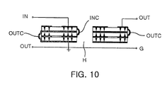
- FIG. 10 illustrates a modified example of FIG. 9 .
- the stacked ring-dot type piezoelectric transformer can include two or more layers of the piezoelectric elements. Under this condition, the input electrodes, the out electrodes and the ground electrodes can be connected themselves together through connecting parts INC, OUTC and GC.
- the input impedance is fitted to the dot size, and the output impedance is fitted to the number of the stacked layers, so that only the impedance of the output side can be lowered.
- the resonance frequency and the anti-resonance frequency of the stacked ring-dot type piezoelectric transformer of the present invention are compared with those of the conventional ring-dot type piezoelectric transformer, and the comparison results are shown in Table 2 below.
- fr indicates the resonance frequency
- fa indicates the anti-resonance frequency
- k indicates oscillation energy/voltage energy.
- the resonance frequency fr and the anti-resonance frequency fa are lowered in the present invention compared with the conventional transformer, while k has slightly increased.
- FIG. 11 illustrates another modified example of FIG. 9 .
- the first modified example of the fourth embodiment is further modified as follows. That is, the piezoelectric transformer can be made round rather than rectangular.
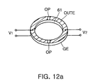
- FIG. 12 illustrates a fifth embodiment of the stacked ring-dot type piezoelectric transformer according to the present invention.
- an upper face of a doughnut shaped piezoelectric element 61 is divided into two mutually electrically isolated parts to form an input electrode INE and an output electrode OUTE.
- a ground electrode GE is formed under the doughnut shaped piezoelectric element 61 , thereby forming a stacked ring-dot type piezoelectric transformer.
- FIG. 12 a is a perspective view of the ring type piezoelectric transformer.
- FIG. 12 b is a sectional view of a single layer piezoelectric transformer. In this ring type transformer, the exposed surface area is increased, and therefore, the heat release temperature is lowered.
- FIG. 12 c is a sectional view of a multi-layer piezoelectric transformer.
- This stacked ring type piezoelectric transformer includes: a first doughnut shaped piezoelectric element 61 a; a first input electrode INE 1 occupying a part of an upper face of the first piezoelectric element 61 a; a first output electrode OUTE 1 occupying another part of the upper face of the first piezoelectric element 61 a, and electrically isolated from the first input electrode INE 1 by an open region OP; a ground electrode GE formed under the first piezoelectric element 61a; a second piezoelectric element 61 b stacked beneath the first piezoelectric element 61 a across the ground terminal GE; and second input and output electrodes INE 2 and OUTE 2 formed under the second piezoelectric element 61 b and opposite to the first input and out electrodes INE 1 and OUTE 1 .
- Both of the first and second input electrodes INE 1 and INE 2 are connected to an input terminal IN, and both of the first and second output electrodes OUTE 1 and OUTE 2 are connected to an output terminal OUT, while the ground electrode GE is connected to a ground terminal G.
- the input capacitance can be increased through stacking, so that the input power can be increased, and that the output capacitance can also be increased. Further, the impedance matching with the load is rendered easier, and thus, the oscillation speed can be lowered, thereby realizing a high output power. Further, the heat release temperature is lowered.
- the conventional ring-dot type piezoelectric transformer is applicable to only the ballast
- the stacked ring-dot type piezoelectric transformer of the present invention is applicable even to adaptor and charger, because the input and output capacitances can be adjusted, and consequently because the adjustment between the load and the source becomes easy.
Landscapes
- Engineering & Computer Science (AREA)
- Power Engineering (AREA)
- Dc-Dc Converters (AREA)
Applications Claiming Priority (2)
| Application Number | Priority Date | Filing Date | Title |
|---|---|---|---|
| KR19990028258 | 1999-07-13 | ||
| KR99-28258 | 1999-07-13 |
Publications (1)
| Publication Number | Publication Date |
|---|---|
| US6346763B1 true US6346763B1 (en) | 2002-02-12 |
Family
ID=19601400
Family Applications (1)
| Application Number | Title | Priority Date | Filing Date |
|---|---|---|---|
| US09/602,510 Expired - Fee Related US6346763B1 (en) | 1999-07-13 | 2000-06-23 | High output stacked piezoelectric transformer |
Country Status (4)
| Country | Link |
|---|---|
| US (1) | US6346763B1 (zh) |
| JP (2) | JP2001060730A (zh) |
| KR (1) | KR100349127B1 (zh) |
| TW (1) | TW492204B (zh) |
Cited By (3)
| Publication number | Priority date | Publication date | Assignee | Title |
|---|---|---|---|---|
| US20040174098A1 (en) * | 2003-03-04 | 2004-09-09 | Yu-Hsiang Hsu | Optimized piezoelectric transformer apparatus with maximum energy conversion efficiency |
| WO2008049394A1 (de) | 2006-10-23 | 2008-05-02 | Epcos Ag | Piezotransformator |
| WO2013052910A3 (en) * | 2011-10-05 | 2013-06-20 | Ross Bird | Slat-constructed autonomic transformers |
Families Citing this family (3)
| Publication number | Priority date | Publication date | Assignee | Title |
|---|---|---|---|---|
| US7122939B2 (en) | 2004-06-25 | 2006-10-17 | Zippy Technology Corp. | Piezoelectric power supply |
| JP2006353056A (ja) * | 2005-06-20 | 2006-12-28 | Nec Tokin Corp | 圧電トランス |
| KR20160026600A (ko) | 2014-09-01 | 2016-03-09 | 주식회사 솔루엠 | 전원 공급 장치 및 방법 |
Citations (5)
| Publication number | Priority date | Publication date | Assignee | Title |
|---|---|---|---|---|
| US2976501A (en) * | 1959-07-30 | 1961-03-21 | Oskar E Mattiat | Impedance transformer |
| US3250017A (en) * | 1962-05-10 | 1966-05-10 | Murgatroyds Salt & Chem | After-treatment of particulate solids |
| US3764848A (en) * | 1972-03-15 | 1973-10-09 | Venitron Corp | Piezoelectric starter and ballast for gaseous discharge lamps |
| US6008565A (en) | 1997-04-18 | 1999-12-28 | Nec Corporation | Laminated piezoelectric transformer |
| US6065196A (en) | 1996-06-11 | 2000-05-23 | Nec Corporation | Method of manufacturing a laminated piezoelectric transformer |
-
2000
- 2000-06-19 TW TW089111990A patent/TW492204B/zh not_active IP Right Cessation
- 2000-06-23 US US09/602,510 patent/US6346763B1/en not_active Expired - Fee Related
- 2000-07-12 KR KR1020000039840A patent/KR100349127B1/ko not_active IP Right Cessation
- 2000-07-12 JP JP2000210991A patent/JP2001060730A/ja active Pending
-
2003
- 2003-12-11 JP JP2003412947A patent/JP2004088132A/ja active Pending
Patent Citations (5)
| Publication number | Priority date | Publication date | Assignee | Title |
|---|---|---|---|---|
| US2976501A (en) * | 1959-07-30 | 1961-03-21 | Oskar E Mattiat | Impedance transformer |
| US3250017A (en) * | 1962-05-10 | 1966-05-10 | Murgatroyds Salt & Chem | After-treatment of particulate solids |
| US3764848A (en) * | 1972-03-15 | 1973-10-09 | Venitron Corp | Piezoelectric starter and ballast for gaseous discharge lamps |
| US6065196A (en) | 1996-06-11 | 2000-05-23 | Nec Corporation | Method of manufacturing a laminated piezoelectric transformer |
| US6008565A (en) | 1997-04-18 | 1999-12-28 | Nec Corporation | Laminated piezoelectric transformer |
Cited By (7)
| Publication number | Priority date | Publication date | Assignee | Title |
|---|---|---|---|---|
| US20040174098A1 (en) * | 2003-03-04 | 2004-09-09 | Yu-Hsiang Hsu | Optimized piezoelectric transformer apparatus with maximum energy conversion efficiency |
| WO2008049394A1 (de) | 2006-10-23 | 2008-05-02 | Epcos Ag | Piezotransformator |
| US20090236948A1 (en) * | 2006-10-23 | 2009-09-24 | Christian Hoffmann | Piezoelectric Transformer |
| US8174169B2 (en) | 2006-10-23 | 2012-05-08 | Epcos Ag | Piezoelectric transformer |
| WO2013052910A3 (en) * | 2011-10-05 | 2013-06-20 | Ross Bird | Slat-constructed autonomic transformers |
| US20140132118A9 (en) * | 2011-10-05 | 2014-05-15 | Ross W. Bird | Slat-constructed autonomic transformers |
| US9337411B2 (en) * | 2011-10-05 | 2016-05-10 | Qortek, Inc. | Slat-constructed autonomic transformers |
Also Published As
| Publication number | Publication date |
|---|---|
| JP2001060730A (ja) | 2001-03-06 |
| TW492204B (en) | 2002-06-21 |
| JP2004088132A (ja) | 2004-03-18 |
| KR100349127B1 (ko) | 2002-08-17 |
| KR20010029928A (ko) | 2001-04-16 |
Similar Documents
| Publication | Publication Date | Title |
|---|---|---|
| US4665465A (en) | Feed-through type multilayer capacitor | |
| EP1087411A3 (en) | Multilayer capacitor | |
| US6346763B1 (en) | High output stacked piezoelectric transformer | |
| KR20090121337A (ko) | 적층 대역 통과 필터 | |
| US6577044B1 (en) | Multi-output composite piezoelectric transformer with expansion vibration mode | |
| US5162970A (en) | Miniature monolithic ceramic coupler for electronic circuits | |
| US6417745B1 (en) | LC filter with a coupling capacitor formed by shared first and second capacitor patterns | |
| US6294783B1 (en) | Infrared sensor | |
| JPS6461111A (en) | Composite parts comprising piezoelectric resonator and capacitor | |
| US6903643B2 (en) | Laminated balun transformer | |
| CN111415808A (zh) | 平面型变压器 | |
| US8098117B2 (en) | LC composite component | |
| US6011451A (en) | Chip type piezoelectric filter having internal common electrodes or a shield electrode | |
| JP3277812B2 (ja) | 表面実装型アンテナ | |
| WO2002027810B1 (en) | Piezoelectric transformer and operating method | |
| JPH06151243A (ja) | 積層型フィルタ | |
| KR100349134B1 (ko) | 고출력용 압전트랜스 | |
| US7852167B2 (en) | Third overtone crystal oscillator | |
| GB1576704A (en) | Oscillator | |
| US6337791B1 (en) | Capacitor featuring internal electrode with pad | |
| JPH0373422U (zh) | ||
| JP2662741B2 (ja) | 共振器 | |
| KR200234436Y1 (ko) | 고주파용 적층형 칩 인덕터 | |
| JPH0679127U (ja) | プリントコイルトランス | |
| KR200299041Y1 (ko) | 전자렌지용 고압 트랜스포머 |
Legal Events
| Date | Code | Title | Description |
|---|---|---|---|
| AS | Assignment |
Owner name: SAMSUNG ELECTRO-MECHANICS CO., LTD., KOREA, REPUBL Free format text: ASSIGNMENT OF ASSIGNORS INTEREST;ASSIGNOR:MOON, YANGHO;REEL/FRAME:010896/0986 Effective date: 20000609 |
|
| FPAY | Fee payment |
Year of fee payment: 4 |
|
| FPAY | Fee payment |
Year of fee payment: 8 |
|
| FEPP | Fee payment procedure |
Free format text: PAYOR NUMBER ASSIGNED (ORIGINAL EVENT CODE: ASPN); ENTITY STATUS OF PATENT OWNER: LARGE ENTITY |
|
| REMI | Maintenance fee reminder mailed | ||
| LAPS | Lapse for failure to pay maintenance fees | ||
| STCH | Information on status: patent discontinuation |
Free format text: PATENT EXPIRED DUE TO NONPAYMENT OF MAINTENANCE FEES UNDER 37 CFR 1.362 |
|
| FP | Lapsed due to failure to pay maintenance fee |
Effective date: 20140212 |