US6313024B1 - Method for forming a semiconductor device - Google Patents
Method for forming a semiconductor device Download PDFInfo
- Publication number
- US6313024B1 US6313024B1 US09/394,190 US39419099A US6313024B1 US 6313024 B1 US6313024 B1 US 6313024B1 US 39419099 A US39419099 A US 39419099A US 6313024 B1 US6313024 B1 US 6313024B1
- Authority
- US
- United States
- Prior art keywords
- layer
- dielectric layer
- conductive
- forming
- conductive support
- Prior art date
- Legal status (The legal status is an assumption and is not a legal conclusion. Google has not performed a legal analysis and makes no representation as to the accuracy of the status listed.)
- Expired - Lifetime
Links
Images


Classifications
-
- H—ELECTRICITY
- H01—ELECTRIC ELEMENTS
- H01L—SEMICONDUCTOR DEVICES NOT COVERED BY CLASS H10
- H01L24/00—Arrangements for connecting or disconnecting semiconductor or solid-state bodies; Methods or apparatus related thereto
- H01L24/01—Means for bonding being attached to, or being formed on, the surface to be connected, e.g. chip-to-package, die-attach, "first-level" interconnects; Manufacturing methods related thereto
- H01L24/02—Bonding areas ; Manufacturing methods related thereto
- H01L24/04—Structure, shape, material or disposition of the bonding areas prior to the connecting process
- H01L24/05—Structure, shape, material or disposition of the bonding areas prior to the connecting process of an individual bonding area
-
- H—ELECTRICITY
- H01—ELECTRIC ELEMENTS
- H01L—SEMICONDUCTOR DEVICES NOT COVERED BY CLASS H10
- H01L23/00—Details of semiconductor or other solid state devices
- H01L23/52—Arrangements for conducting electric current within the device in operation from one component to another, i.e. interconnections, e.g. wires, lead frames
- H01L23/522—Arrangements for conducting electric current within the device in operation from one component to another, i.e. interconnections, e.g. wires, lead frames including external interconnections consisting of a multilayer structure of conductive and insulating layers inseparably formed on the semiconductor body
- H01L23/532—Arrangements for conducting electric current within the device in operation from one component to another, i.e. interconnections, e.g. wires, lead frames including external interconnections consisting of a multilayer structure of conductive and insulating layers inseparably formed on the semiconductor body characterised by the materials
- H01L23/5329—Insulating materials
-
- H—ELECTRICITY
- H01—ELECTRIC ELEMENTS
- H01L—SEMICONDUCTOR DEVICES NOT COVERED BY CLASS H10
- H01L24/00—Arrangements for connecting or disconnecting semiconductor or solid-state bodies; Methods or apparatus related thereto
- H01L24/01—Means for bonding being attached to, or being formed on, the surface to be connected, e.g. chip-to-package, die-attach, "first-level" interconnects; Manufacturing methods related thereto
- H01L24/02—Bonding areas ; Manufacturing methods related thereto
- H01L24/03—Manufacturing methods
-
- H—ELECTRICITY
- H01—ELECTRIC ELEMENTS
- H01L—SEMICONDUCTOR DEVICES NOT COVERED BY CLASS H10
- H01L2224/00—Indexing scheme for arrangements for connecting or disconnecting semiconductor or solid-state bodies and methods related thereto as covered by H01L24/00
- H01L2224/01—Means for bonding being attached to, or being formed on, the surface to be connected, e.g. chip-to-package, die-attach, "first-level" interconnects; Manufacturing methods related thereto
- H01L2224/02—Bonding areas; Manufacturing methods related thereto
- H01L2224/0212—Auxiliary members for bonding areas, e.g. spacers
- H01L2224/02122—Auxiliary members for bonding areas, e.g. spacers being formed on the semiconductor or solid-state body
- H01L2224/02163—Auxiliary members for bonding areas, e.g. spacers being formed on the semiconductor or solid-state body on the bonding area
- H01L2224/02165—Reinforcing structures
- H01L2224/02166—Collar structures
-
- H—ELECTRICITY
- H01—ELECTRIC ELEMENTS
- H01L—SEMICONDUCTOR DEVICES NOT COVERED BY CLASS H10
- H01L2224/00—Indexing scheme for arrangements for connecting or disconnecting semiconductor or solid-state bodies and methods related thereto as covered by H01L24/00
- H01L2224/01—Means for bonding being attached to, or being formed on, the surface to be connected, e.g. chip-to-package, die-attach, "first-level" interconnects; Manufacturing methods related thereto
- H01L2224/02—Bonding areas; Manufacturing methods related thereto
- H01L2224/04—Structure, shape, material or disposition of the bonding areas prior to the connecting process
- H01L2224/05—Structure, shape, material or disposition of the bonding areas prior to the connecting process of an individual bonding area
- H01L2224/0554—External layer
- H01L2224/05599—Material
- H01L2224/056—Material with a principal constituent of the material being a metal or a metalloid, e.g. boron [B], silicon [Si], germanium [Ge], arsenic [As], antimony [Sb], tellurium [Te] and polonium [Po], and alloys thereof
- H01L2224/05617—Material with a principal constituent of the material being a metal or a metalloid, e.g. boron [B], silicon [Si], germanium [Ge], arsenic [As], antimony [Sb], tellurium [Te] and polonium [Po], and alloys thereof the principal constituent melting at a temperature of greater than or equal to 400°C and less than 950°C
- H01L2224/05624—Aluminium [Al] as principal constituent
-
- H—ELECTRICITY
- H01—ELECTRIC ELEMENTS
- H01L—SEMICONDUCTOR DEVICES NOT COVERED BY CLASS H10
- H01L2224/00—Indexing scheme for arrangements for connecting or disconnecting semiconductor or solid-state bodies and methods related thereto as covered by H01L24/00
- H01L2224/01—Means for bonding being attached to, or being formed on, the surface to be connected, e.g. chip-to-package, die-attach, "first-level" interconnects; Manufacturing methods related thereto
- H01L2224/02—Bonding areas; Manufacturing methods related thereto
- H01L2224/04—Structure, shape, material or disposition of the bonding areas prior to the connecting process
- H01L2224/05—Structure, shape, material or disposition of the bonding areas prior to the connecting process of an individual bonding area
- H01L2224/0554—External layer
- H01L2224/05599—Material
- H01L2224/056—Material with a principal constituent of the material being a metal or a metalloid, e.g. boron [B], silicon [Si], germanium [Ge], arsenic [As], antimony [Sb], tellurium [Te] and polonium [Po], and alloys thereof
- H01L2224/05638—Material with a principal constituent of the material being a metal or a metalloid, e.g. boron [B], silicon [Si], germanium [Ge], arsenic [As], antimony [Sb], tellurium [Te] and polonium [Po], and alloys thereof the principal constituent melting at a temperature of greater than or equal to 950°C and less than 1550°C
- H01L2224/05647—Copper [Cu] as principal constituent
-
- H—ELECTRICITY
- H01—ELECTRIC ELEMENTS
- H01L—SEMICONDUCTOR DEVICES NOT COVERED BY CLASS H10
- H01L2924/00—Indexing scheme for arrangements or methods for connecting or disconnecting semiconductor or solid-state bodies as covered by H01L24/00
- H01L2924/01—Chemical elements
- H01L2924/01004—Beryllium [Be]
-
- H—ELECTRICITY
- H01—ELECTRIC ELEMENTS
- H01L—SEMICONDUCTOR DEVICES NOT COVERED BY CLASS H10
- H01L2924/00—Indexing scheme for arrangements or methods for connecting or disconnecting semiconductor or solid-state bodies as covered by H01L24/00
- H01L2924/01—Chemical elements
- H01L2924/01005—Boron [B]
-
- H—ELECTRICITY
- H01—ELECTRIC ELEMENTS
- H01L—SEMICONDUCTOR DEVICES NOT COVERED BY CLASS H10
- H01L2924/00—Indexing scheme for arrangements or methods for connecting or disconnecting semiconductor or solid-state bodies as covered by H01L24/00
- H01L2924/01—Chemical elements
- H01L2924/01006—Carbon [C]
-
- H—ELECTRICITY
- H01—ELECTRIC ELEMENTS
- H01L—SEMICONDUCTOR DEVICES NOT COVERED BY CLASS H10
- H01L2924/00—Indexing scheme for arrangements or methods for connecting or disconnecting semiconductor or solid-state bodies as covered by H01L24/00
- H01L2924/01—Chemical elements
- H01L2924/01013—Aluminum [Al]
-
- H—ELECTRICITY
- H01—ELECTRIC ELEMENTS
- H01L—SEMICONDUCTOR DEVICES NOT COVERED BY CLASS H10
- H01L2924/00—Indexing scheme for arrangements or methods for connecting or disconnecting semiconductor or solid-state bodies as covered by H01L24/00
- H01L2924/01—Chemical elements
- H01L2924/01014—Silicon [Si]
-
- H—ELECTRICITY
- H01—ELECTRIC ELEMENTS
- H01L—SEMICONDUCTOR DEVICES NOT COVERED BY CLASS H10
- H01L2924/00—Indexing scheme for arrangements or methods for connecting or disconnecting semiconductor or solid-state bodies as covered by H01L24/00
- H01L2924/01—Chemical elements
- H01L2924/01019—Potassium [K]
-
- H—ELECTRICITY
- H01—ELECTRIC ELEMENTS
- H01L—SEMICONDUCTOR DEVICES NOT COVERED BY CLASS H10
- H01L2924/00—Indexing scheme for arrangements or methods for connecting or disconnecting semiconductor or solid-state bodies as covered by H01L24/00
- H01L2924/01—Chemical elements
- H01L2924/01022—Titanium [Ti]
-
- H—ELECTRICITY
- H01—ELECTRIC ELEMENTS
- H01L—SEMICONDUCTOR DEVICES NOT COVERED BY CLASS H10
- H01L2924/00—Indexing scheme for arrangements or methods for connecting or disconnecting semiconductor or solid-state bodies as covered by H01L24/00
- H01L2924/01—Chemical elements
- H01L2924/01029—Copper [Cu]
-
- H—ELECTRICITY
- H01—ELECTRIC ELEMENTS
- H01L—SEMICONDUCTOR DEVICES NOT COVERED BY CLASS H10
- H01L2924/00—Indexing scheme for arrangements or methods for connecting or disconnecting semiconductor or solid-state bodies as covered by H01L24/00
- H01L2924/01—Chemical elements
- H01L2924/01033—Arsenic [As]
-
- H—ELECTRICITY
- H01—ELECTRIC ELEMENTS
- H01L—SEMICONDUCTOR DEVICES NOT COVERED BY CLASS H10
- H01L2924/00—Indexing scheme for arrangements or methods for connecting or disconnecting semiconductor or solid-state bodies as covered by H01L24/00
- H01L2924/01—Chemical elements
- H01L2924/01073—Tantalum [Ta]
-
- H—ELECTRICITY
- H01—ELECTRIC ELEMENTS
- H01L—SEMICONDUCTOR DEVICES NOT COVERED BY CLASS H10
- H01L2924/00—Indexing scheme for arrangements or methods for connecting or disconnecting semiconductor or solid-state bodies as covered by H01L24/00
- H01L2924/01—Chemical elements
- H01L2924/01074—Tungsten [W]
-
- H—ELECTRICITY
- H01—ELECTRIC ELEMENTS
- H01L—SEMICONDUCTOR DEVICES NOT COVERED BY CLASS H10
- H01L2924/00—Indexing scheme for arrangements or methods for connecting or disconnecting semiconductor or solid-state bodies as covered by H01L24/00
- H01L2924/01—Chemical elements
- H01L2924/01078—Platinum [Pt]
-
- H—ELECTRICITY
- H01—ELECTRIC ELEMENTS
- H01L—SEMICONDUCTOR DEVICES NOT COVERED BY CLASS H10
- H01L2924/00—Indexing scheme for arrangements or methods for connecting or disconnecting semiconductor or solid-state bodies as covered by H01L24/00
- H01L2924/049—Nitrides composed of metals from groups of the periodic table
- H01L2924/0494—4th Group
- H01L2924/04941—TiN
-
- H—ELECTRICITY
- H01—ELECTRIC ELEMENTS
- H01L—SEMICONDUCTOR DEVICES NOT COVERED BY CLASS H10
- H01L2924/00—Indexing scheme for arrangements or methods for connecting or disconnecting semiconductor or solid-state bodies as covered by H01L24/00
- H01L2924/049—Nitrides composed of metals from groups of the periodic table
- H01L2924/0495—5th Group
- H01L2924/04953—TaN
-
- H—ELECTRICITY
- H01—ELECTRIC ELEMENTS
- H01L—SEMICONDUCTOR DEVICES NOT COVERED BY CLASS H10
- H01L2924/00—Indexing scheme for arrangements or methods for connecting or disconnecting semiconductor or solid-state bodies as covered by H01L24/00
- H01L2924/049—Nitrides composed of metals from groups of the periodic table
- H01L2924/0504—14th Group
- H01L2924/05042—Si3N4
-
- H—ELECTRICITY
- H01—ELECTRIC ELEMENTS
- H01L—SEMICONDUCTOR DEVICES NOT COVERED BY CLASS H10
- H01L2924/00—Indexing scheme for arrangements or methods for connecting or disconnecting semiconductor or solid-state bodies as covered by H01L24/00
- H01L2924/10—Details of semiconductor or other solid state devices to be connected
- H01L2924/11—Device type
- H01L2924/14—Integrated circuits
-
- H—ELECTRICITY
- H01—ELECTRIC ELEMENTS
- H01L—SEMICONDUCTOR DEVICES NOT COVERED BY CLASS H10
- H01L2924/00—Indexing scheme for arrangements or methods for connecting or disconnecting semiconductor or solid-state bodies as covered by H01L24/00
- H01L2924/30—Technical effects
- H01L2924/301—Electrical effects
- H01L2924/30105—Capacitance
Definitions
- This invention relates generally to integrated circuits, and more specifically to a conductive support structure within an integrated circuit and its method of formation.
- FIGS. 1-7 illustrate, in cross-section, process steps in accordance with one embodiment of the present invention.
- FIG. 8 illustrates, in cross-section, process steps in accordance with an alternative embodiment of the present invention.
- FIG. 9 illustrates, in top-down view, a portion of an integrated circuit in accordance with one embodiment of the present invention.
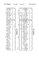
- FIG. 1 Shown in FIG. 1 is a portion 10 of an integrated circuit structure in accordance with one embodiment of the present invention.
- the integrated circuit structure comprises a semiconductor substrate 12 having a bond pad region 20 (periphery) and a scribe line region 18 , and a dielectric layer 14 .
- semiconductor substrate 12 is a monocrystalline silicon substrate.
- semiconductor substrate 12 may be a silicon-on-insulator substrate, a silicon-on-sapphire substrate, or the like.
- Dielectric layer 14 is formed using a material having a high modulus of elasticity (Young's modulus).
- the modulus of elasticity of a material is an indicator of its rigidity or stiffness.
- a material having a high modulus of elasticity is any material having a modulus of elasticity greater than approximately 15.00 Giga Pascals (GPa).
- dielectric layer 14 is a layer of plasma deposited oxide which is formed using tetraethoxysilane (TEOS) as a source gas and has a modulus of elasticity greater than approximately 50 GPa.
- dielectric layer 14 may be a layer of silicon nitride, a layer of phosphosilicate glass (PSG), a layer of borophosphosilicate glass (BPSG), a silicon oxynitride layer, a thermal oxide layer, or a combination thereof.
- an etch stop layer 22 is formed overlying dielectric layer 14 and then a dielectric layer 24 is formed overlying etch stop layer 22 .
- a polish stop layer 26 is then formed overlying dielectric layer 24 .
- etch stop layer 22 is a layer of silicon oxynitride which is formed using conventional plasma deposition techniques.
- etch stop layer 22 may be a layer of plasma deposited silicon nitride, a boron nitride layer, a silicon oxide, or the like.
- Dielectric layer 24 is formed using a material having a low modulus of elasticity (Young's modulus), and in one embodiment dielectric layer 24 is a low dielectric constant (low-k) material.
- a low modulus of elasticity material is a material having a Young's modulus measuring less than approximately 15 GPa and a low-k material is a material having a dielectric constant below approximately 3.6.
- dielectric layer 24 is a layer of porous oxide, such as xerogel, having a Young's modulus ranging from approximately 0.2 to 0.1 GPa and a dielectric constant of approximately 1.8.
- dielectric layer 24 may be formed using other dielectric materials including, aerogel, polyimide, parylene, biscyclobutenes, fluorocarbons, such as Teflon, polyarylether-based materials, spin on glass, polysiloxanes, silsesquioxanes, carbon-containing silicon oxide, or the like.
- dielectric materials having a modulus of elasticity of less than 15.0 are mechanically weak or compressible, as compared to silicon dioxide, which has a Young's modulus measuring approximately 80 GPa. As a result, the horizontal and vertical stresses applied during subsequent processing, specifically during chemical mechanical polishing, are such that low modulus of elasticity dielectric materials are susceptible to deformation or damage.
- polish stop layer 26 is a layer of silicon oxynitride.
- polish stop layer 26 may be a layer of plasma deposited silicon nitride, a boron nitride layer, or the like.
- a portion of polish stop layer 26 , a portion of dielectric layer 24 and a portion of etch stop layer 22 are removed to form openings 25 .
- a conductive member 28 is then formed within each opening 25 .
- conductive member 28 comprises tantalum nitride and copper and is formed by depositing a layer of tantalum nitride within opening 25 and then forming a layer of copper overlying the tantalum nitride layer. Chemical mechanical polishing is then used to remove portions of the copper layer and the tantalum nitride layer thereby forming conductive member 28 , wherein conductive member 28 comprises a remaining portion of the tantalum nitride layer and a remaining portion of the copper layer.
- the tantalum nitride layer is deposited using conventional sputtering techniques.
- the copper layer is formed by first sputter depositing a thin layer of copper onto the tantalum nitride layer using conventional sputtering techniques, and then electroplating a thick copper layer onto the sputtered copper layer.
- the electroplated copper layer may be deposited using a plating solution comprising copper (Cu), copper sulfate (Cu 2 SO 4 ), sulfuric acid (H 2 SO 4 ), and chloride ions, such as those from hydrochloric acid (HCI).
- the electric current density is modified near the edges of the semiconductor substrate during the copper electroplating process in order to improve the copper electroplating uniformity, as is described in U.S. patent application Ser. No. 08/856,459, which is assigned to the assignee of the present application.
- the subject matter of U.S. patent application Ser. No. 08/856,459 is expressly incorporated herein by reference.
- Portions of the copper layer and the tantalum nitride layer can then be removed with a chemical mechanical polishing process that uses a polishing slurry comprising hydrogen peroxide, ammonium citrate, alumina, 1,2,4-triazole, and deionized water, as is described in U.S. patent application Ser. No. 08/954,190, which is assigned to the assignee of the present application.
- a polishing slurry comprising hydrogen peroxide, ammonium citrate, alumina, 1,2,4-triazole, and deionized water
- conductive members 28 may be formed using other conductive materials, such as titanium, tungsten, aluminum, titanium nitride, tungsten nitride, titanium-tungsten (TiW), tantalum silicon nitride, tantalum, or the like.
- conductive members 28 may also be formed using other electroplating techniques, other electroplating solutions, polishing techniques, polishing slurries, or other deposition techniques, such as chemical vapor deposition or electroless deposition.
- conductive members 28 are formed at the same time that a given level of conductive interconnect is formed within the device region of the integrated circuit, however, they are not electrically connected to devices or functional circuit elements that lie within the device region or testable circuit elements (test structures) in the scribe line region. For example, in one embodiment, conductive members 28 are formed at the same time that the first level of conductive interconnect is formed in the device region. Thus, the formation of conductive members 28 does not require additional processing steps, such as a masking step or an etching step. More importantly, conductive members 28 provide support for the surrounding portions of dielectric layer 24 that lie within bonding pad region 20 and scribe line region 18 , during subsequent processing. For example, conductive members 28 provide support for the surrounding portions of dielectric layer 24 during subsequent chemical mechanical polishing processes, as will now be discussed.
- dielectric layer 24 is formed using a material that has a low modulus of elasticity
- areas of dielectric layer 24 where interconnects are not usually formed such as the bond pad region ( 20 ) and scribe line region ( 18 ) can easily be compressed or deformed by subsequent chemical mechanical polishing processes that exert compressive and shear forces on them.
- Placing conductive members 28 in these areas provides stability and support to dielectric layer 24 , improving its ability to withstand these forces, thereby preventing it from becoming damaged.
- conductive members 28 provide support to portions of dielectric layer 24 that lie within bond pad region 20 and scribe line region 18 . More specifically, they minimize compression and deformation of dielectric layer 24 , within bond pad region 20 and scribe line region 18 , produced by the polishing process.
- a passivation layer 30 is formed overlying conductive members 28 .
- a dielectric layer 32 is then formed overlying passivation layer 30 .
- An etch stop layer 34 is then formed overlying the dielectric layer 32 .
- a dielectric layer 36 is formed overlying etch stop layer 34 and a polish stop layer 38 is formed overlying dielectric layer 36 .
- passivation layer 30 is a layer of silicon oxynitride which is formed using conventional plasma deposition techniques.
- passivation layer 30 may be a layer of plasma deposited silicon nitride, a boron nitride layer, a silicon dioxide layer formed using TEOS as a source gas, or the like.
- Dielectric layer 32 is formed using a material having a low modulus of elasticity (Young's modulus), and in one embodiment dielectric layer 32 is a low dielectric constant (low-k) material.
- dielectric layer 32 is a layer of porous oxide, such as xerogel, having a Young's modulus ranging from approximately 0.2 to 0.1 GPa and a dielectric constant of approximately 1.8.
- dielectric layer 32 may be formed using other dielectric materials including, aerogel, polyimide, parylene, biscyclobutenes, fluorocarbons, such as Teflon, polyarylether-based materials, spin on glass, polysiloxanes, silsesquioxanes, carbon-containing silicon oxide, or the like.
- fluorocarbons such as Teflon, polyarylether-based materials, spin on glass, polysiloxanes, silsesquioxanes, carbon-containing silicon oxide, or the like.
- a combination of the foregoing materials may also be used to form the dielectric layer 32 .
- etch stop layer 34 is a layer of silicon oxynitride.
- etch stop layer 34 may be a layer of plasma deposited silicon nitride, a boron nitride layer, or the like.
- Dielectric layer 36 is formed using a material having a low modulus of elasticity (Young's modulus), and in one embodiment dielectric layer 36 is a low dielectric constant (low-k) material.
- dielectric layer 36 is a layer of porous oxide, such as xerogel, having a Young's modulus ranging from approximately 0.2 to 0.1 GPa and a dielectric constant of approximately 1.8.
- dielectric layer 36 may be formed using other dielectric materials including, aerogel, polyimide, parylene, biscyclobutenes, fluorocarbons, such as Teflon, polyarylether-based materials, spin on glass, polysiloxanes, silsesquioxanes, carbon-containing silicon oxide, or the like.
- fluorocarbons such as Teflon, polyarylether-based materials, spin on glass, polysiloxanes, silsesquioxanes, carbon-containing silicon oxide, or the like.
- a combination of the foregoing materials may also be used to form the dielectric layer 36 .
- polish stop layer 38 is a layer of silicon oxynitride.
- polish stop layer 38 may be a layer of plasma deposited silicon nitride, a boron nitride layer, or the like.
- a portion of the polish stop layer 38 , a portion of the dielectric layer 36 , a portion of the etch stop layer 34 , a portion of the dielectric layer 32 and a portion of the passivation layer 30 are removed to form openings 39 .
- a conductive member 40 is then formed within each opening 39 , as previously described in FIG. 3 .
- Each conductive member 40 contacts an underlying conductive member 28 and is electrically shorted to the underlying conductive member 28 .
- conductive members 40 are formed at the same time that a given level of conductive interconnect is formed within the device region of the integrated circuit, however, they are not electrically connected to devices or functional circuit elements that lie within the device region or testable circuit elements (test structures) in the scribe line region.
- conductive members 40 are formed at the same time that the second level of conductive interconnect is formed within the device region.
- the formation of conductive members 40 does not require any additional processing steps, such as a masking step or an etching step.
- conductive members 40 provide support for the surrounding portions of dielectric layer 32 and dielectric layer 36 within bonding pad region 20 and scribe line region 18 , during subsequent processing. For example, during a subsequent chemical mechanical polishing processing step, as will now be discussed.
- dielectric layer 32 and dielectric layer 36 are formed using a material that has a low modulus of elasticity, areas of dielectric layers 32 and 36 where interconnects are not usually formed, such as the bond pad region ( 20 ) and scribe line region ( 18 ), can easily be compressed or deformed by subsequent chemical mechanical polishing processes that exert compressive and shear forces on them. Placing conductive members 40 in these areas, however, provides stability and support to dielectric layer 32 and dielectric layer 36 , improving their ability to withstand these forces, thereby preventing them from becoming damaged.
- conductive members 40 support and stabilize portions of dielectric layer 32 and dielectric layer 36 that lie within bond pad region 20 and scribe line region 18 . More specifically, they minimize compression and deformation of dielectric layer 32 and dielectric layer 36 within bond pad region 20 and scribe line 18 produced by the polishing process.
- a passivation layer 42 is formed overlying conductive members 40 .
- a dielectric layer 44 is then formed overlying passivation layer 42 .
- An etch stop layer 46 is then formed overlying the dielectric layer 44 .
- a dielectric layer 48 is formed overlying etch stop layer 46 and a polish stop layer 50 is formed overlying dielectric layer 48 .
- passivation layer 42 is a layer of silicon oxynitride which is formed using conventional plasma deposition techniques.
- passivation layer 42 may be a layer of plasma deposited silicon nitride, a boron nitride layer, or the like.
- Dielectric layer 44 is formed using a material having a low modulus of elasticity (Young's modulus), and in one embodiment dielectric layer 44 is a low dielectric constant (low-k) material.
- dielectric layer 44 is a layer of porous oxide, such as xerogel, having a Young's modulus ranging from approximately 0.2 to 0.1 GPa and a dielectric constant of approximately 1.8.
- dielectric layer 44 may be formed using other dielectric materials including, aerogel, polyimide, parylene, biscyclobutenes, fluorocarbons, such as Teflon, polyarylether-based materials, spin on glass, polysiloxanes, silsesquioxanes, carbon-containing silicon oxide, or the like.
- fluorocarbons such as Teflon, polyarylether-based materials, spin on glass, polysiloxanes, silsesquioxanes, carbon-containing silicon oxide, or the like.
- etch stop layer 46 is a layer of silicon oxynitride.
- etch stop layer 46 may be a layer of plasma deposited silicon nitride, a boron nitride layer, or the like.
- Dielectric layer 48 is formed using a material having a low modulus of elasticity (Young's modulus), and in one embodiment dielectric layer 48 is a low dielectric constant (low-k) material.
- dielectric layer 48 is a layer of porous oxide, such as xerogel, having a Young's modulus ranging from approximately 0.2 to 0.1 GPa and a dielectric constant of approximately 1.8.
- dielectric layer 48 may be formed using other dielectric materials including, aerogel, polyimide, parylene, biscyclobutenes, fluorocarbons, such as Teflon, polyarylether-based materials, spin on glass, polysiloxanes, silsesquioxanes, carbon-containing silicon oxide, or the like.
- polish stop layer 50 is a layer of silicon oxynitride.
- polish stop layer 50 may be a layer of plasma deposited silicon nitride, a boron nitride layer, or the like.
- a portion of the polish stop layer 50 , a portion of the dielectric layer 48 , a portion of the etch stop layer 46 , a portion of the dielectric layer 44 and a portion of the passivation layer 42 are removed to form openings 49 .
- a conductive member 52 is then formed within each opening 49 , as previously described in FIG. 5 to form conductive member 40 within each opening 39 .
- the combination of conductive member 52 , conductive member 40 , and conductive member 28 form a conductive support structure 54 . As shown in FIG. 6, conductive members 52 contact and are electrically shorted to the underlying conductive members 40 .
- conductive members 52 are formed at the same time that a given level of conductive interconnect is formed within the device region of the integrated circuit, however, they are not electrically connected to devices or functional circuit elements that lie within the device region or testable circuit elements (test structures) in the scribe line region. For example, in one embodiment, conductive members 52 are formed at the same time that the third level of conductive interconnect is formed within the device region. Thus, the formation of conductive members 52 does not require additional processing steps, such as an additional masking step or etching step. More importantly, conductive members 52 provide support for the surrounding portions of dielectric layer 44 and dielectric layer 48 within bonding pad region 20 and scribe line region 18 , during subsequent processing as discussed previously with conductive members 40 .
- conductive support structures 54 provide support to regions of the low-k dielectric layers that have a relatively low density of interconnect features, such as the bond pad region ( 20 ) and the scribe line region ( 18 ). For example, in FIG. 6 each conductive support structure 54 extends through dielectric layer 48 , dielectric layer 44 , dielectric layer 36 , dielectric layer 32 , and dielectric layer 24 and thus each of them provides support for these dielectric layers.
- passivation layer 65 is then formed overlying conductive support structures 54 , and a dielectric layer 66 is formed overlying passivation layer 65 .
- passivation layer 65 is a layer of silicon oxynitride which is formed using conventional plasma deposition techniques.
- passivation layer 65 may be a layer of plasma deposited silicon nitride, a boron nitride layer, or the like.
- dielectric layer 66 is a layer of plasma deposited oxide which is formed using TEOS as a source gas.
- dielectric layer 66 may be a layer of silicon nitride, a layer of PSG, a layer of BPSG, a silicon oxynitride layer, a fluorinated oxide, an SOG material, or a combination thereof.
- a conductive bonding pad 90 is then formed overlying dielectric layer 66 .
- Conductive bonding pad 90 is electrically connected to semiconductor devices (not shown) that lie within the device region of the integrated circuit.
- conductive bonding pad 90 is formed by depositing a conductive layer comprising aluminum, such as aluminum, aluminum-silicon, aluminum-copper, aluminum-silicon-copper, or the like, and then patterning and etching the conductive layer using conventional techniques.
- conductive bond pad 90 may be formed using other conductive materials, such as copper, tungsten, titanium, or the like.
- a passivation layer 92 is formed overlying dielectric layer 66 and conductive bonding pad 90 . The passivation layer 92 is then patterned and etched to define a bond pad opening 94 .
- passivation layer 92 is a layer of plasma deposited silicon nitride.
- passivation layer 92 may be a layer of PSG, an SOG layer, a silicon oxynitride layer, or a combination thereof.
- FIG. 8 Shown in FIG. 8 is a portion 75 of an integrated circuit structure in accordance with an alternative embodiment of the present invention.
- conductive support structures 41 comprise conductive members 40 and conductive members 28 of FIG. 5 .
- a passivation layer 76 is formed overlying conductive support structures 41 .
- a dielectric layer 78 is then formed overlying passivation layer 76 .
- An etch stop layer 80 is then formed overlying the dielectric layer 78 .
- a dielectric layer 82 is formed overlying etch stop layer 80 and a polish stop layer 84 is formed overlying dielectric layer 82 .
- passivation layer 76 is a layer of silicon oxynitride which is formed using conventional plasma deposition techniques.
- passivation layer 76 may be a layer of plasma deposited silicon nitride, a boron nitride layer, or the like.
- Dielectric layer 78 is formed using a material having a high modulus of elasticity (Young's modulus).
- dielectric layer 78 is a layer of plasma deposited oxide which is formed using tetraethoxysilane (TEOS) as a source gas and has a modulus of elasticity greater than approximately 50 GPa.
- TEOS tetraethoxysilane
- dielectric layer 78 may be a layer of silicon nitride, a layer of phosphosilicate glass (PSG), a layer of borophosphosilicate glass (BPSG), a silicon oxynitride layer, a layer of fluorinated plasma oxide, or a combination thereof.
- PSG phosphosilicate glass
- BPSG borophosphosilicate glass
- silicon oxynitride layer a layer of fluorinated plasma oxide, or a combination thereof.
- etch stop layer 80 is a layer of silicon oxynitride.
- etch stop layer 80 may be a layer of plasma deposited silicon nitride, a boron nitride layer, an SOG material, or the like.
- Dielectric layer 82 is formed using a material having a high modulus of elasticity (Young's modulus).
- dielectric layer 82 is a layer of plasma deposited oxide which is formed using tetraethoxysilane (TEOS) as a source gas and has a modulus of elasticity greater than approximately 50 GPa.
- TEOS tetraethoxysilane
- dielectric layer 82 may be a layer of silicon nitride, a layer of phosphosilicate glass (PSG), a layer of borophosphosilicate glass (BPSG), a silicon oxynitride layer, a layer of fluorinated plasma oxide, or a combination thereof.
- PSG phosphosilicate glass
- BPSG borophosphosilicate glass
- silicon oxynitride layer a layer of fluorinated plasma oxide, or a combination thereof.
- polish stop layer 84 is a layer of silicon oxynitride.
- polish stop layer 84 may be a layer of plasma deposited silicon nitride, a boron nitride layer, or the like.
- passivation layer 85 is then formed overlying polish stop layer 84 , and a dielectric layer 86 is formed overlying passivation layer 85 .
- passivation layer 85 is a layer of silicon oxynitride which is formed using conventional plasma deposition techniques.
- passivation layer 85 may be a layer of plasma deposited silicon nitride, a boron nitride layer, or the like.
- dielectric layer 86 is a layer of plasma deposited oxide which is formed using TEOS as a source gas.
- dielectric layer 86 may be a layer of silicon nitride, a layer of PSG, a layer of BPSG, an SOG layer, a silicon oxynitride layer, or a combination thereof.
- a conductive bonding pad 88 is then formed overlying dielectric layer 86 .
- Conductive bonding pad 88 is electrically connected to semiconductor devices (not shown) that lie within the device region of the integrated circuit.
- conductive bonding pad 88 is formed by depositing a conductive layer comprising aluminum, such as aluminum, aluminum-silicon, aluminum-copper, aluminum-silicon-copper, or the like, and then patterning the conductive layer using conventional etching techniques.
- conductive bond pad 88 may be formed using other conductive materials, such as copper, tungsten, titanium, or the like.
- a passivation layer 89 is formed overlying dielectric layer 86 and conductive bonding pad 88 , and then patterned form a bond pad opening 91 .
- passivation layer 89 is a layer of plasma deposited silicon nitride.
- passivation layer 89 may be a layer of PSG, an SOG layer, a silicon oxynitride layer, or a combination thereof.
- constructive support structures 41 need not extend through dielectric layer 78 and dielectric layer 82 because they are not formed using a material which has a low Young's modulus. Thus, these dielectric layers need not be supported or stabilized during subsequent processing.
- the present invention allows dielectric layers with both low and high Young's modulus'to be used to fabricate integrated circuit structures, such as that shown in FIG. 8 . Specifically, the present invention allows one or more dielectric layers having a low Young's modulus to be placed between two other dielectric layers that have a high Young's modulus. For example, in FIG. 8 dielectric layer 36 , dielectric layer 32 and dielectric layer 24 which have a low Young's modulus have been placed between dielectric layer 14 and dielectric layer 82 have a high Young's modulus.
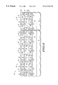
- FIG. 9 Shown in FIG. 9 is a top down view of a portion 100 of an integrated circuit structure in accordance with one embodiment of the present invention.
- the integrated circuit structure 100 comprises a first integrated circuit die 102 , a second integrated circuit die 103 , and a scribe line region 104 .
- the scribe line region 104 lies between the first integrated circuit die 102 and the second integrated circuit die 103 , and comprises conductive support structures 114 , an alignment key 105 , and a test structure 115 .
- the first integrated circuit die 102 comprises an edge seal region 106 , a device region 109 , conductive bond pads 110 , a bond pad region 111 , and conductive support structures 112 .
- the second integrated circuit die 103 comprises an edge seal region 108 , a device region 116 , conductive bond pads 118 , a bond pad region 120 , and conductive support structures 122 .
- conductive support structures 112 lie within bond pad region 111 .
- Conductive support structures 112 lie outside the perimeter of conductive bond pads 110 , and lie between conductive bond pads 110 and edge seal region 106 .
- conductive support structures 112 lie between device region 109 and conductive bond pads 110 .
- conductive support structures 122 lie within bond pad region 120 .
- Conductive support structures 122 lie outside the perimeter of conductive bond pads 118 , and lie between conductive bond pads 118 and edge seal region 108 .
- conductive support structures 122 lie between device region 116 and conductive bond pads 118 .
Landscapes
- Engineering & Computer Science (AREA)
- Computer Hardware Design (AREA)
- Microelectronics & Electronic Packaging (AREA)
- Power Engineering (AREA)
- Manufacturing & Machinery (AREA)
- Physics & Mathematics (AREA)
- Condensed Matter Physics & Semiconductors (AREA)
- General Physics & Mathematics (AREA)
- Internal Circuitry In Semiconductor Integrated Circuit Devices (AREA)
- Semiconductor Integrated Circuits (AREA)
Abstract
Description
Claims (20)
Priority Applications (1)
| Application Number | Priority Date | Filing Date | Title |
|---|---|---|---|
| US09/394,190 US6313024B1 (en) | 1998-11-13 | 1999-09-10 | Method for forming a semiconductor device |
Applications Claiming Priority (2)
| Application Number | Priority Date | Filing Date | Title |
|---|---|---|---|
| US09/191,353 US6037668A (en) | 1998-11-13 | 1998-11-13 | Integrated circuit having a support structure |
| US09/394,190 US6313024B1 (en) | 1998-11-13 | 1999-09-10 | Method for forming a semiconductor device |
Related Parent Applications (1)
| Application Number | Title | Priority Date | Filing Date |
|---|---|---|---|
| US09/191,353 Continuation US6037668A (en) | 1998-11-13 | 1998-11-13 | Integrated circuit having a support structure |
Publications (1)
| Publication Number | Publication Date |
|---|---|
| US6313024B1 true US6313024B1 (en) | 2001-11-06 |
Family
ID=22705135
Family Applications (2)
| Application Number | Title | Priority Date | Filing Date |
|---|---|---|---|
| US09/191,353 Expired - Lifetime US6037668A (en) | 1998-11-13 | 1998-11-13 | Integrated circuit having a support structure |
| US09/394,190 Expired - Lifetime US6313024B1 (en) | 1998-11-13 | 1999-09-10 | Method for forming a semiconductor device |
Family Applications Before (1)
| Application Number | Title | Priority Date | Filing Date |
|---|---|---|---|
| US09/191,353 Expired - Lifetime US6037668A (en) | 1998-11-13 | 1998-11-13 | Integrated circuit having a support structure |
Country Status (2)
| Country | Link |
|---|---|
| US (2) | US6037668A (en) |
| JP (1) | JP4615078B2 (en) |
Cited By (35)
| Publication number | Priority date | Publication date | Assignee | Title |
|---|---|---|---|---|
| US20020187634A1 (en) * | 1998-05-18 | 2002-12-12 | Mukul Saran | Fine pitch system and method for reinforcing bond pads in semiconductor devices |
| US6566244B1 (en) * | 2002-05-03 | 2003-05-20 | Lsi Logic Corporation | Process for improving mechanical strength of layers of low k dielectric material |
| US20030104690A1 (en) * | 1999-06-25 | 2003-06-05 | Nec Corporation | Semiconductor device |
| US6605861B2 (en) * | 2001-01-17 | 2003-08-12 | Mitsubishi Denki Kabushiki Kaisha | Semiconductor device |
| US20030235018A1 (en) * | 2002-06-21 | 2003-12-25 | Shubneesh Batra | Method and structures for reduced parasitic capacitance in integrated circuit metallizatons |
| US20040058520A1 (en) * | 2002-09-20 | 2004-03-25 | Burrell Lloyd G. | Support structures for wirebond regions of contact pads over low modulus materials |
| US20040087078A1 (en) * | 2002-02-20 | 2004-05-06 | Agarwala Birendra N. | Edge seal for a semiconductor device |
| WO2004040646A1 (en) * | 2002-10-22 | 2004-05-13 | Infineon Technologies Ag | Electronic component with an integrated passive electronic component and method for production thereof |
| US20040094840A1 (en) * | 2001-03-28 | 2004-05-20 | Hitoshi Sakamoto | Integrated circuit structure |
| US6803662B2 (en) * | 2001-12-21 | 2004-10-12 | International Business Machines Corporation | Low dielectric constant material reinforcement for improved electromigration reliability |
| US20050032353A1 (en) * | 2003-08-06 | 2005-02-10 | Hsi-Kuei Cheng | Method for reducing defects in post passivation interconnect process |
| US20050127529A1 (en) * | 2003-12-10 | 2005-06-16 | Taiwan Semiconductor Manufacturing Co., Ltd. | Structure and method for reinforcing a bond pad on a chip |
| KR100605428B1 (en) | 2003-09-08 | 2006-07-28 | 가부시끼가이샤 르네사스 테크놀로지 | Semiconductor device and method of manufacturing the same |
| US20060264040A1 (en) * | 2005-05-09 | 2006-11-23 | Shuichi Takada | Semiconductor device |
| US20070049049A1 (en) * | 2005-08-29 | 2007-03-01 | Yeh-Sheng Cheng | Test-key for checking interconnect and corresponding checking method |
| US20070080464A1 (en) * | 2005-10-12 | 2007-04-12 | Thomas Goebel | Support structures for semiconductor devices |
| US20070210442A1 (en) * | 2005-01-11 | 2007-09-13 | Freescale Semiconductor, Inc. | Method and apparatus for providing structural support for interconnect pad while allowing signal conductance |
| US20070267755A1 (en) * | 2006-05-16 | 2007-11-22 | Vo Nhat D | Integrated circuit having pads and input/output (i/o) cells |
| US20070267748A1 (en) * | 2006-05-16 | 2007-11-22 | Tran Tu-Anh N | Integrated circuit having pads and input/output (i/o) cells |
| US20080116544A1 (en) * | 2006-11-22 | 2008-05-22 | Tessera, Inc. | Packaged semiconductor chips with array |
| US20080153265A1 (en) * | 2006-12-21 | 2008-06-26 | Texas Instruments Incorporated | Semiconductor Device Manufactured Using an Etch to Separate Wafer into Dies and Increase Device Space on a Wafer |
| US20090250792A1 (en) * | 2008-04-02 | 2009-10-08 | Joung-Wei Liou | Curing Low-k Dielectrics for Improving Mechanical Strength |
| US20100171920A1 (en) * | 2007-06-22 | 2010-07-08 | Tomohiro Nishiyama | Display device and method for producing the same |
| US20100200987A1 (en) * | 2005-10-07 | 2010-08-12 | Renesas Technology Corp. | Semiconductor Device and a Method of Manufacturing the Same |
| US20110012259A1 (en) * | 2006-11-22 | 2011-01-20 | Tessera, Inc. | Packaged semiconductor chips |
| US20120018868A1 (en) * | 2010-07-23 | 2012-01-26 | Tessera Research Llc | Microelectronic elements having metallic pads overlying vias |
| US8735287B2 (en) | 2007-07-31 | 2014-05-27 | Invensas Corp. | Semiconductor packaging process using through silicon vias |
| US8796135B2 (en) | 2010-07-23 | 2014-08-05 | Tessera, Inc. | Microelectronic elements with rear contacts connected with via first or via middle structures |
| US8796828B2 (en) | 2010-12-08 | 2014-08-05 | Tessera, Inc. | Compliant interconnects in wafers |
| US8809190B2 (en) | 2010-09-17 | 2014-08-19 | Tessera, Inc. | Multi-function and shielded 3D interconnects |
| US8847380B2 (en) | 2010-09-17 | 2014-09-30 | Tessera, Inc. | Staged via formation from both sides of chip |
| US9099296B2 (en) | 2010-12-02 | 2015-08-04 | Tessera, Inc. | Stacked microelectronic assembly with TSVS formed in stages with plural active chips |
| US9245083B2 (en) | 2011-10-13 | 2016-01-26 | Globalfoundries Inc. | Method, structures and method of designing reduced delamination integrated circuits |
| US9269692B2 (en) | 2010-12-02 | 2016-02-23 | Tessera, Inc. | Stacked microelectronic assembly with TSVS formed in stages and carrier above chip |
| US9640437B2 (en) | 2010-07-23 | 2017-05-02 | Tessera, Inc. | Methods of forming semiconductor elements using micro-abrasive particle stream |
Families Citing this family (44)
| Publication number | Priority date | Publication date | Assignee | Title |
|---|---|---|---|---|
| JPH11307633A (en) * | 1997-11-17 | 1999-11-05 | Sony Corp | Semiconductor device having film of low permittivity and manufacture thereof |
| KR100292403B1 (en) * | 1997-12-30 | 2001-07-12 | 윤종용 | Interlayer dielectric film of semiconductor device and method for forming film |
| US6232662B1 (en) * | 1998-07-14 | 2001-05-15 | Texas Instruments Incorporated | System and method for bonding over active integrated circuits |
| JP2974022B1 (en) * | 1998-10-01 | 1999-11-08 | ヤマハ株式会社 | Bonding pad structure of semiconductor device |
| JP2000174123A (en) * | 1998-12-09 | 2000-06-23 | Nec Corp | Semiconductor device and manufacture thereof |
| US8021976B2 (en) * | 2002-10-15 | 2011-09-20 | Megica Corporation | Method of wire bonding over active area of a semiconductor circuit |
| JP4460669B2 (en) | 1999-03-19 | 2010-05-12 | 株式会社東芝 | Semiconductor device |
| JP2001223269A (en) * | 2000-02-10 | 2001-08-17 | Nec Corp | Semiconductor device and manufacturing method therefor |
| US6362091B1 (en) * | 2000-03-14 | 2002-03-26 | Intel Corporation | Method for making a semiconductor device having a low-k dielectric layer |
| US6495917B1 (en) * | 2000-03-17 | 2002-12-17 | International Business Machines Corporation | Method and structure of column interconnect |
| GB2368851B (en) * | 2000-06-07 | 2003-12-10 | Tokuyama Corp | Process for producing sintered aluminium nitride furnished with via holes |
| US6879046B2 (en) * | 2001-06-28 | 2005-04-12 | Agere Systems Inc. | Split barrier layer including nitrogen-containing portion and oxygen-containing portion |
| KR100400047B1 (en) * | 2001-11-19 | 2003-09-29 | 삼성전자주식회사 | Bonding pad structure of semiconductor device and method for forming thereof |
| US6645832B2 (en) * | 2002-02-20 | 2003-11-11 | Intel Corporation | Etch stop layer for silicon (Si) via etch in three-dimensional (3-D) wafer-to-wafer vertical stack |
| US6784556B2 (en) * | 2002-04-19 | 2004-08-31 | Kulicke & Soffa Investments, Inc. | Design of interconnection pads with separated probing and wire bonding regions |
| JP4005873B2 (en) * | 2002-08-15 | 2007-11-14 | 株式会社東芝 | Semiconductor device |
| US6958542B2 (en) | 2002-09-03 | 2005-10-25 | Kabushiki Kaisha Toshiba | Semiconductor device |
| US6621167B1 (en) * | 2002-09-23 | 2003-09-16 | United Microelectronics Corp. | Metal interconnect structure |
| US7288845B2 (en) * | 2002-10-15 | 2007-10-30 | Marvell Semiconductor, Inc. | Fabrication of wire bond pads over underlying active devices, passive devices and/or dielectric layers in integrated circuits |
| JP3811473B2 (en) * | 2003-02-25 | 2006-08-23 | 富士通株式会社 | Semiconductor device |
| JP3802002B2 (en) * | 2003-03-27 | 2006-07-26 | 三星電子株式会社 | Manufacturing method of semiconductor device |
| US7495343B1 (en) | 2003-07-31 | 2009-02-24 | Nvidia Corporation | Pad over active circuit system and method with frame support structure |
| US7453158B2 (en) * | 2003-07-31 | 2008-11-18 | Nvidia Corporation | Pad over active circuit system and method with meshed support structure |
| DE10342996A1 (en) * | 2003-09-17 | 2005-04-21 | Infineon Technologies Ag | Semiconductor arrangement comprises a substrate with integrated electronic switching elements, layer stacks arranged over the substrate, and a dummy structure arranged in two layer stacks for mechanically stabilizing the stacks |
| EP1519411A3 (en) * | 2003-09-26 | 2010-01-13 | Panasonic Corporation | Semiconductor device and method for fabricating the same |
| JP2005142351A (en) * | 2003-11-06 | 2005-06-02 | Nec Electronics Corp | Semiconductor device and its manufacturing method |
| US7056820B2 (en) * | 2003-11-20 | 2006-06-06 | International Business Machines Corporation | Bond pad |
| JP4619705B2 (en) * | 2004-01-15 | 2011-01-26 | 株式会社東芝 | Semiconductor device |
| WO2005096364A1 (en) * | 2004-03-31 | 2005-10-13 | Nec Corporation | Semiconductor device and method for manufacturing same |
| DE102004025658A1 (en) * | 2004-05-26 | 2005-12-29 | Infineon Technologies Ag | Method for producing a semiconductor circuit and corresponding semiconductor circuit |
| JP4401874B2 (en) | 2004-06-21 | 2010-01-20 | 株式会社ルネサステクノロジ | Semiconductor device |
| JP4636839B2 (en) | 2004-09-24 | 2011-02-23 | パナソニック株式会社 | Electronic devices |
| JP2006140404A (en) * | 2004-11-15 | 2006-06-01 | Renesas Technology Corp | Semiconductor device |
| KR100675275B1 (en) * | 2004-12-16 | 2007-01-26 | 삼성전자주식회사 | Semiconductor device and pad arrangement method thereof |
| KR100602131B1 (en) * | 2004-12-30 | 2006-07-19 | 동부일렉트로닉스 주식회사 | Semiconductor device and method for fabricating the same |
| JP2007005536A (en) * | 2005-06-23 | 2007-01-11 | Renesas Technology Corp | Semiconductor device |
| US7276435B1 (en) | 2006-06-02 | 2007-10-02 | Freescale Semiconductor, Inc. | Die level metal density gradient for improved flip chip package reliability |
| KR101328552B1 (en) * | 2007-11-16 | 2013-11-13 | 삼성전자주식회사 | Non-volatile memory devices and methdos of forming the same |
| US8946874B2 (en) * | 2011-01-25 | 2015-02-03 | Taiwan Semiconductor Manufacturing Company, Ltd. | IC in-process solution to reduce thermal neutrons soft error rate |
| US9064707B2 (en) * | 2011-09-14 | 2015-06-23 | Micronas Gmbh | Bonding contact area on a semiconductor substrate |
| JP5932079B2 (en) * | 2015-02-26 | 2016-06-08 | ルネサスエレクトロニクス株式会社 | Semiconductor device |
| US9666514B2 (en) * | 2015-04-14 | 2017-05-30 | Invensas Corporation | High performance compliant substrate |
| CN109643745B (en) * | 2015-08-03 | 2023-07-14 | 亮锐控股有限公司 | Semiconductor light emitting device with reflective side coating |
| US9922947B2 (en) * | 2016-04-28 | 2018-03-20 | Stmicroelectronics S.R.L. | Bonding pad structure over active circuitry |
Citations (13)
| Publication number | Priority date | Publication date | Assignee | Title |
|---|---|---|---|---|
| US4729063A (en) | 1985-02-22 | 1988-03-01 | Mitsubishi Denki Kabushiki Kaisha | Plastic molded semiconductor integrated circuit device with nail section |
| US4984061A (en) | 1987-05-15 | 1991-01-08 | Kabushiki Kaisha Toshiba | Semiconductor device in which wiring layer is formed below bonding pad |
| US5036383A (en) | 1989-04-27 | 1991-07-30 | Kabushiki Kaisha Toshiba | Semiconductor device having an improved bonding pad |
| US5220199A (en) | 1988-09-13 | 1993-06-15 | Hitachi, Ltd. | Semiconductor integrated circuit device in which a semiconductor chip is mounted with solder bumps for mounting to a wiring substrate |
| US5270256A (en) | 1991-11-27 | 1993-12-14 | Intel Corporation | Method of forming a guard wall to reduce delamination effects |
| US5287002A (en) | 1991-06-17 | 1994-02-15 | Motorola, Inc. | Planar multi-layer metal bonding pad |
| US5394013A (en) | 1990-11-28 | 1995-02-28 | Mitsubishi Denki Kabushiki Kaisha | Semiconductor device with an elevated bonding pad |
| US5478781A (en) * | 1993-06-21 | 1995-12-26 | International Business Machines Corporation | Polyimide-insulated cube package of stacked semiconductor device chips |
| US5485038A (en) | 1993-07-15 | 1996-01-16 | Hughes Aircraft Company | Microelectronic circuit substrate structure including photoimageable epoxy dielectric layers |
| US5621246A (en) | 1993-07-09 | 1997-04-15 | Fujitsu Limited | Substrate for mounting integrated circuit semiconductor chips |
| US5728628A (en) * | 1994-05-27 | 1998-03-17 | Texas Instruments Incorporated | Two-step metal etch process for selective gap fill of submicron inter-connects and structure for same |
| US5773899A (en) | 1993-09-30 | 1998-06-30 | Consorzio Per La Ricerca Sulla Microelettronica Nel Mezzogiorno | Bonding pad for a semiconductor chip |
| US5976710A (en) * | 1991-08-05 | 1999-11-02 | International Business Machines Corporation | Low TCE polyimides as improved insulator in multilayer interconnect structures |
Family Cites Families (9)
| Publication number | Priority date | Publication date | Assignee | Title |
|---|---|---|---|---|
| JP2919488B2 (en) * | 1989-07-05 | 1999-07-12 | 株式会社日立製作所 | Semiconductor integrated circuit device |
| JPH07169807A (en) * | 1993-12-16 | 1995-07-04 | Nippondenso Co Ltd | Semiconductor wafer |
| JPH10247664A (en) * | 1997-03-04 | 1998-09-14 | Hitachi Ltd | Semiconductor integrated circuit device and manufacture thereof |
| US5959453A (en) * | 1997-10-29 | 1999-09-28 | Western Atlas International, Inc. | Radial NMR well logging apparatus and method |
| JP3638778B2 (en) * | 1997-03-31 | 2005-04-13 | 株式会社ルネサステクノロジ | Semiconductor integrated circuit device and manufacturing method thereof |
| US5923047A (en) * | 1997-04-21 | 1999-07-13 | Lsi Logic Corporation | Semiconductor die having sacrificial bond pads for die test |
| US6143396A (en) * | 1997-05-01 | 2000-11-07 | Texas Instruments Incorporated | System and method for reinforcing a bond pad |
| JPH1197645A (en) * | 1997-09-19 | 1999-04-09 | Nec Corp | Semiconductor storage device |
| JP4424768B2 (en) * | 1998-11-10 | 2010-03-03 | 株式会社ルネサステクノロジ | Semiconductor device and manufacturing method thereof |
-
1998
- 1998-11-13 US US09/191,353 patent/US6037668A/en not_active Expired - Lifetime
-
1999
- 1999-09-10 US US09/394,190 patent/US6313024B1/en not_active Expired - Lifetime
- 1999-11-09 JP JP31764299A patent/JP4615078B2/en not_active Expired - Fee Related
Patent Citations (13)
| Publication number | Priority date | Publication date | Assignee | Title |
|---|---|---|---|---|
| US4729063A (en) | 1985-02-22 | 1988-03-01 | Mitsubishi Denki Kabushiki Kaisha | Plastic molded semiconductor integrated circuit device with nail section |
| US4984061A (en) | 1987-05-15 | 1991-01-08 | Kabushiki Kaisha Toshiba | Semiconductor device in which wiring layer is formed below bonding pad |
| US5220199A (en) | 1988-09-13 | 1993-06-15 | Hitachi, Ltd. | Semiconductor integrated circuit device in which a semiconductor chip is mounted with solder bumps for mounting to a wiring substrate |
| US5036383A (en) | 1989-04-27 | 1991-07-30 | Kabushiki Kaisha Toshiba | Semiconductor device having an improved bonding pad |
| US5394013A (en) | 1990-11-28 | 1995-02-28 | Mitsubishi Denki Kabushiki Kaisha | Semiconductor device with an elevated bonding pad |
| US5287002A (en) | 1991-06-17 | 1994-02-15 | Motorola, Inc. | Planar multi-layer metal bonding pad |
| US5976710A (en) * | 1991-08-05 | 1999-11-02 | International Business Machines Corporation | Low TCE polyimides as improved insulator in multilayer interconnect structures |
| US5270256A (en) | 1991-11-27 | 1993-12-14 | Intel Corporation | Method of forming a guard wall to reduce delamination effects |
| US5478781A (en) * | 1993-06-21 | 1995-12-26 | International Business Machines Corporation | Polyimide-insulated cube package of stacked semiconductor device chips |
| US5621246A (en) | 1993-07-09 | 1997-04-15 | Fujitsu Limited | Substrate for mounting integrated circuit semiconductor chips |
| US5485038A (en) | 1993-07-15 | 1996-01-16 | Hughes Aircraft Company | Microelectronic circuit substrate structure including photoimageable epoxy dielectric layers |
| US5773899A (en) | 1993-09-30 | 1998-06-30 | Consorzio Per La Ricerca Sulla Microelettronica Nel Mezzogiorno | Bonding pad for a semiconductor chip |
| US5728628A (en) * | 1994-05-27 | 1998-03-17 | Texas Instruments Incorporated | Two-step metal etch process for selective gap fill of submicron inter-connects and structure for same |
Non-Patent Citations (1)
| Title |
|---|
| Saran et al, "Elimination of Bond-pad Damage through Structural Reinforcement of Intermetal Dielectrics," 36th Annual International Reliability Physics Symposium, IEEE 98CH36173, pp. 225-231 (1998). |
Cited By (82)
| Publication number | Priority date | Publication date | Assignee | Title |
|---|---|---|---|---|
| US20020187634A1 (en) * | 1998-05-18 | 2002-12-12 | Mukul Saran | Fine pitch system and method for reinforcing bond pads in semiconductor devices |
| US6818540B2 (en) * | 1998-05-18 | 2004-11-16 | Texas Instruments Incorporated | Fine pitch system and method for reinforcing bond pads in semiconductor devices |
| US20030104690A1 (en) * | 1999-06-25 | 2003-06-05 | Nec Corporation | Semiconductor device |
| US6605861B2 (en) * | 2001-01-17 | 2003-08-12 | Mitsubishi Denki Kabushiki Kaisha | Semiconductor device |
| US20040094840A1 (en) * | 2001-03-28 | 2004-05-20 | Hitoshi Sakamoto | Integrated circuit structure |
| US6803662B2 (en) * | 2001-12-21 | 2004-10-12 | International Business Machines Corporation | Low dielectric constant material reinforcement for improved electromigration reliability |
| US20040087078A1 (en) * | 2002-02-20 | 2004-05-06 | Agarwala Birendra N. | Edge seal for a semiconductor device |
| US6734090B2 (en) * | 2002-02-20 | 2004-05-11 | International Business Machines Corporation | Method of making an edge seal for a semiconductor device |
| US7163883B2 (en) * | 2002-02-20 | 2007-01-16 | International Business Machines Corporation | Edge seal for a semiconductor device |
| US6566244B1 (en) * | 2002-05-03 | 2003-05-20 | Lsi Logic Corporation | Process for improving mechanical strength of layers of low k dielectric material |
| US20030235018A1 (en) * | 2002-06-21 | 2003-12-25 | Shubneesh Batra | Method and structures for reduced parasitic capacitance in integrated circuit metallizatons |
| US7160795B2 (en) * | 2002-06-21 | 2007-01-09 | Micron Technology, Inc. | Method and structures for reduced parasitic capacitance in integrated circuit metallizations |
| US20040058520A1 (en) * | 2002-09-20 | 2004-03-25 | Burrell Lloyd G. | Support structures for wirebond regions of contact pads over low modulus materials |
| US6908841B2 (en) | 2002-09-20 | 2005-06-21 | Infineon Technologies Ag | Support structures for wirebond regions of contact pads over low modulus materials |
| WO2004040646A1 (en) * | 2002-10-22 | 2004-05-13 | Infineon Technologies Ag | Electronic component with an integrated passive electronic component and method for production thereof |
| US20050199934A1 (en) * | 2002-10-22 | 2005-09-15 | Infineon Technologies Ag | Electronic component having an integrated passive electronic component and associated production method |
| US7193263B2 (en) | 2002-10-22 | 2007-03-20 | Infineon Technologies Ag | Electronic component having an integrated passive electronic component and associated production method |
| CN100459112C (en) * | 2002-10-22 | 2009-02-04 | 因芬尼昂技术股份公司 | Electronic component having an integrated passive electronic component and associated production method |
| US20050032353A1 (en) * | 2003-08-06 | 2005-02-10 | Hsi-Kuei Cheng | Method for reducing defects in post passivation interconnect process |
| US20060145332A1 (en) * | 2003-08-06 | 2006-07-06 | Hsi-Kuei Cheng | Semiconductor devices having post passivation interconnections with a second connection pattern |
| US7026233B2 (en) * | 2003-08-06 | 2006-04-11 | Taiwan Semiconductor Manufacturing Company, Ltd. | Method for reducing defects in post passivation interconnect process |
| US7528478B2 (en) | 2003-08-06 | 2009-05-05 | Taiwan Semiconductor Manufacturing Company, Ltd. | Semiconductor devices having post passivation interconnections and a buffer layer |
| KR100605428B1 (en) | 2003-09-08 | 2006-07-28 | 가부시끼가이샤 르네사스 테크놀로지 | Semiconductor device and method of manufacturing the same |
| US7081679B2 (en) * | 2003-12-10 | 2006-07-25 | Taiwan Semiconductor Manufacturing Co., Ltd. | Structure and method for reinforcing a bond pad on a chip |
| US20050127529A1 (en) * | 2003-12-10 | 2005-06-16 | Taiwan Semiconductor Manufacturing Co., Ltd. | Structure and method for reinforcing a bond pad on a chip |
| US7626276B2 (en) * | 2005-01-11 | 2009-12-01 | Freescale Semiconductor, Inc. | Method and apparatus for providing structural support for interconnect pad while allowing signal conductance |
| US20070210442A1 (en) * | 2005-01-11 | 2007-09-13 | Freescale Semiconductor, Inc. | Method and apparatus for providing structural support for interconnect pad while allowing signal conductance |
| US20060264040A1 (en) * | 2005-05-09 | 2006-11-23 | Shuichi Takada | Semiconductor device |
| US7893536B2 (en) * | 2005-05-09 | 2011-02-22 | Kabushiki Kaisha Toshiba | Semiconductor device |
| US20090065775A1 (en) * | 2005-08-29 | 2009-03-12 | United Microelectronics Corp. | Test-key for checking interconnect and corresponding checking method |
| US20070049049A1 (en) * | 2005-08-29 | 2007-03-01 | Yeh-Sheng Cheng | Test-key for checking interconnect and corresponding checking method |
| US8278765B2 (en) * | 2005-08-29 | 2012-10-02 | United Microelectronics Corp. | Test-key for checking interconnect |
| US7514278B2 (en) * | 2005-08-29 | 2009-04-07 | United Microelectronics Corp. | Test-key for checking interconnect and corresponding checking method |
| TWI475604B (en) * | 2005-10-07 | 2015-03-01 | Renesas Electronics Corp | Semiconductor device |
| US10304867B2 (en) | 2005-10-07 | 2019-05-28 | Renesas Electronics Corporation | Semiconductor device and a method of manufacturing the same |
| US8624403B2 (en) | 2005-10-07 | 2014-01-07 | Renesas Electronics Corporation | Semiconductor device and a method of manufacturing the same |
| US10957719B2 (en) | 2005-10-07 | 2021-03-23 | Renesas Electronics Corporation | Semiconductor device and a method of manufacturing the same |
| US8338968B2 (en) | 2005-10-07 | 2012-12-25 | Renesas Electronics Corporation | Semiconductor device and a method of manufacturing the same |
| US9929185B2 (en) | 2005-10-07 | 2018-03-27 | Renesas Electronics Corporation | Semiconductor device and a method of manufacturing the same |
| US9159650B2 (en) | 2005-10-07 | 2015-10-13 | Renesas Electronics Corporation | Semiconductor device and a method of manufacturing the same |
| US9576924B2 (en) | 2005-10-07 | 2017-02-21 | Renesas Electronics Corporation | Semiconductor device and a method of manufacturing the same |
| US8183142B2 (en) * | 2005-10-07 | 2012-05-22 | Renesas Electronics Corporation | Semiconductor device and a method of manufacturing the same |
| US20100200987A1 (en) * | 2005-10-07 | 2010-08-12 | Renesas Technology Corp. | Semiconductor Device and a Method of Manufacturing the Same |
| US20100022085A1 (en) * | 2005-10-12 | 2010-01-28 | Thomas Goebel | Method of Forming Support Structures for Semiconductor Devices |
| US7626268B2 (en) * | 2005-10-12 | 2009-12-01 | Infineon Technologies Ag | Support structures for semiconductor devices |
| US20070080464A1 (en) * | 2005-10-12 | 2007-04-12 | Thomas Goebel | Support structures for semiconductor devices |
| US7858448B2 (en) * | 2005-10-12 | 2010-12-28 | Infineon Technologies Ag | Method of forming support structures for semiconductor devices |
| US20070267748A1 (en) * | 2006-05-16 | 2007-11-22 | Tran Tu-Anh N | Integrated circuit having pads and input/output (i/o) cells |
| US7808117B2 (en) | 2006-05-16 | 2010-10-05 | Freescale Semiconductor, Inc. | Integrated circuit having pads and input/output (I/O) cells |
| US20070267755A1 (en) * | 2006-05-16 | 2007-11-22 | Vo Nhat D | Integrated circuit having pads and input/output (i/o) cells |
| US8569876B2 (en) | 2006-11-22 | 2013-10-29 | Tessera, Inc. | Packaged semiconductor chips with array |
| US20110012259A1 (en) * | 2006-11-22 | 2011-01-20 | Tessera, Inc. | Packaged semiconductor chips |
| US9070678B2 (en) | 2006-11-22 | 2015-06-30 | Tessera, Inc. | Packaged semiconductor chips with array |
| US8653644B2 (en) | 2006-11-22 | 2014-02-18 | Tessera, Inc. | Packaged semiconductor chips with array |
| US8704347B2 (en) | 2006-11-22 | 2014-04-22 | Tessera, Inc. | Packaged semiconductor chips |
| US20080116544A1 (en) * | 2006-11-22 | 2008-05-22 | Tessera, Inc. | Packaged semiconductor chips with array |
| US9548254B2 (en) | 2006-11-22 | 2017-01-17 | Tessera, Inc. | Packaged semiconductor chips with array |
| WO2008079691A3 (en) * | 2006-12-21 | 2008-08-28 | Texas Instruments Inc | Semiconductor die with separation trench etch and passivation |
| WO2008079691A2 (en) * | 2006-12-21 | 2008-07-03 | Texas Instruments Incorporated | Semiconductor die with separation trench etch and passivation |
| US20080153265A1 (en) * | 2006-12-21 | 2008-06-26 | Texas Instruments Incorporated | Semiconductor Device Manufactured Using an Etch to Separate Wafer into Dies and Increase Device Space on a Wafer |
| US20100171920A1 (en) * | 2007-06-22 | 2010-07-08 | Tomohiro Nishiyama | Display device and method for producing the same |
| US8735287B2 (en) | 2007-07-31 | 2014-05-27 | Invensas Corp. | Semiconductor packaging process using through silicon vias |
| US8853858B2 (en) * | 2008-04-02 | 2014-10-07 | Taiwan Semiconductor Manufacturing Company, Ltd. | Curing low-k dielectrics for improving mechanical strength |
| US8258629B2 (en) * | 2008-04-02 | 2012-09-04 | Taiwan Semiconductor Manufacturing Company, Ltd. | Curing low-k dielectrics for improving mechanical strength |
| US20090250792A1 (en) * | 2008-04-02 | 2009-10-08 | Joung-Wei Liou | Curing Low-k Dielectrics for Improving Mechanical Strength |
| US20120018868A1 (en) * | 2010-07-23 | 2012-01-26 | Tessera Research Llc | Microelectronic elements having metallic pads overlying vias |
| US9640437B2 (en) | 2010-07-23 | 2017-05-02 | Tessera, Inc. | Methods of forming semiconductor elements using micro-abrasive particle stream |
| US8796135B2 (en) | 2010-07-23 | 2014-08-05 | Tessera, Inc. | Microelectronic elements with rear contacts connected with via first or via middle structures |
| US8791575B2 (en) * | 2010-07-23 | 2014-07-29 | Tessera, Inc. | Microelectronic elements having metallic pads overlying vias |
| US8847380B2 (en) | 2010-09-17 | 2014-09-30 | Tessera, Inc. | Staged via formation from both sides of chip |
| US8809190B2 (en) | 2010-09-17 | 2014-08-19 | Tessera, Inc. | Multi-function and shielded 3D interconnects |
| US10354942B2 (en) | 2010-09-17 | 2019-07-16 | Tessera, Inc. | Staged via formation from both sides of chip |
| US9847277B2 (en) | 2010-09-17 | 2017-12-19 | Tessera, Inc. | Staged via formation from both sides of chip |
| US9355948B2 (en) | 2010-09-17 | 2016-05-31 | Tessera, Inc. | Multi-function and shielded 3D interconnects |
| US9362203B2 (en) | 2010-09-17 | 2016-06-07 | Tessera, Inc. | Staged via formation from both sides of chip |
| US9620437B2 (en) | 2010-12-02 | 2017-04-11 | Tessera, Inc. | Stacked microelectronic assembly with TSVS formed in stages and carrier above chip |
| US9368476B2 (en) | 2010-12-02 | 2016-06-14 | Tessera, Inc. | Stacked microelectronic assembly with TSVs formed in stages with plural active chips |
| US9269692B2 (en) | 2010-12-02 | 2016-02-23 | Tessera, Inc. | Stacked microelectronic assembly with TSVS formed in stages and carrier above chip |
| US9099296B2 (en) | 2010-12-02 | 2015-08-04 | Tessera, Inc. | Stacked microelectronic assembly with TSVS formed in stages with plural active chips |
| US9224649B2 (en) | 2010-12-08 | 2015-12-29 | Tessera, Inc. | Compliant interconnects in wafers |
| US8796828B2 (en) | 2010-12-08 | 2014-08-05 | Tessera, Inc. | Compliant interconnects in wafers |
| US9245083B2 (en) | 2011-10-13 | 2016-01-26 | Globalfoundries Inc. | Method, structures and method of designing reduced delamination integrated circuits |
Also Published As
| Publication number | Publication date |
|---|---|
| JP4615078B2 (en) | 2011-01-19 |
| US6037668A (en) | 2000-03-14 |
| JP2000150521A (en) | 2000-05-30 |
Similar Documents
| Publication | Publication Date | Title |
|---|---|---|
| US6313024B1 (en) | Method for forming a semiconductor device | |
| US7514354B2 (en) | Methods for forming damascene wiring structures having line and plug conductors formed from different materials | |
| US6198170B1 (en) | Bonding pad and support structure and method for their fabrication | |
| US6071809A (en) | Methods for forming high-performing dual-damascene interconnect structures | |
| US6627539B1 (en) | Method of forming dual-damascene interconnect structures employing low-k dielectric materials | |
| US7115995B2 (en) | Structural reinforcement of highly porous low k dielectric films by Cu diffusion barrier structures | |
| US6417094B1 (en) | Dual-damascene interconnect structures and methods of fabricating same | |
| US6989604B1 (en) | Conformal barrier liner in an integrated circuit interconnect | |
| US6727590B2 (en) | Semiconductor device with internal bonding pad | |
| US20070007653A1 (en) | Interconnects with improved reliability | |
| US7109557B2 (en) | Sacrificial dielectric planarization layer | |
| US5960316A (en) | Method to fabricate unlanded vias with a low dielectric constant material as an intraline dielectric | |
| US6426558B1 (en) | Metallurgy for semiconductor devices | |
| US6465867B1 (en) | Amorphous and gradated barrier layer for integrated circuit interconnects | |
| US6251789B1 (en) | Selective slurries for the formation of conductive structures | |
| US6403466B1 (en) | Post-CMP-Cu deposition and CMP to eliminate surface voids | |
| US6348732B1 (en) | Amorphized barrier layer for integrated circuit interconnects | |
| US6417566B1 (en) | Void eliminating seed layer and conductor core integrated circuit interconnects | |
| US6541286B1 (en) | Imaging of integrated circuit interconnects | |
| US6498397B1 (en) | Seed layer with annealed region for integrated circuit interconnects | |
| US20020127849A1 (en) | Method of manufacturing dual damascene structure | |
| US6501177B1 (en) | Atomic layer barrier layer for integrated circuit interconnects | |
| US6455938B1 (en) | Integrated circuit interconnect shunt layer | |
| US20240096796A1 (en) | Integrated circuit device | |
| US6504251B1 (en) | Heat/cold amorphized barrier layer for integrated circuit interconnects |
Legal Events
| Date | Code | Title | Description |
|---|---|---|---|
| STCF | Information on status: patent grant |
Free format text: PATENTED CASE |
|
| AS | Assignment |
Owner name: FREESCALE SEMICONDUCTOR, INC., TEXAS Free format text: ASSIGNMENT OF ASSIGNORS INTEREST;ASSIGNOR:MOTOROLA, INC.;REEL/FRAME:015698/0657 Effective date: 20040404 Owner name: FREESCALE SEMICONDUCTOR, INC.,TEXAS Free format text: ASSIGNMENT OF ASSIGNORS INTEREST;ASSIGNOR:MOTOROLA, INC.;REEL/FRAME:015698/0657 Effective date: 20040404 |
|
| FPAY | Fee payment |
Year of fee payment: 4 |
|
| AS | Assignment |
Owner name: CITIBANK, N.A. AS COLLATERAL AGENT, NEW YORK Free format text: SECURITY AGREEMENT;ASSIGNORS:FREESCALE SEMICONDUCTOR, INC.;FREESCALE ACQUISITION CORPORATION;FREESCALE ACQUISITION HOLDINGS CORP.;AND OTHERS;REEL/FRAME:018855/0129 Effective date: 20061201 Owner name: CITIBANK, N.A. AS COLLATERAL AGENT,NEW YORK Free format text: SECURITY AGREEMENT;ASSIGNORS:FREESCALE SEMICONDUCTOR, INC.;FREESCALE ACQUISITION CORPORATION;FREESCALE ACQUISITION HOLDINGS CORP.;AND OTHERS;REEL/FRAME:018855/0129 Effective date: 20061201 |
|
| FPAY | Fee payment |
Year of fee payment: 8 |
|
| AS | Assignment |
Owner name: CITIBANK, N.A., AS COLLATERAL AGENT,NEW YORK Free format text: SECURITY AGREEMENT;ASSIGNOR:FREESCALE SEMICONDUCTOR, INC.;REEL/FRAME:024397/0001 Effective date: 20100413 Owner name: CITIBANK, N.A., AS COLLATERAL AGENT, NEW YORK Free format text: SECURITY AGREEMENT;ASSIGNOR:FREESCALE SEMICONDUCTOR, INC.;REEL/FRAME:024397/0001 Effective date: 20100413 |
|
| FPAY | Fee payment |
Year of fee payment: 12 |
|
| AS | Assignment |
Owner name: CITIBANK, N.A., AS NOTES COLLATERAL AGENT, NEW YOR Free format text: SECURITY AGREEMENT;ASSIGNOR:FREESCALE SEMICONDUCTOR, INC.;REEL/FRAME:030633/0424 Effective date: 20130521 |
|
| AS | Assignment |
Owner name: CITIBANK, N.A., AS NOTES COLLATERAL AGENT, NEW YOR Free format text: SECURITY AGREEMENT;ASSIGNOR:FREESCALE SEMICONDUCTOR, INC.;REEL/FRAME:031591/0266 Effective date: 20131101 |
|
| AS | Assignment |
Owner name: FREESCALE SEMICONDUCTOR, INC., TEXAS Free format text: PATENT RELEASE;ASSIGNOR:CITIBANK, N.A., AS COLLATERAL AGENT;REEL/FRAME:037356/0553 Effective date: 20151207 Owner name: FREESCALE SEMICONDUCTOR, INC., TEXAS Free format text: PATENT RELEASE;ASSIGNOR:CITIBANK, N.A., AS COLLATERAL AGENT;REEL/FRAME:037354/0225 Effective date: 20151207 Owner name: FREESCALE SEMICONDUCTOR, INC., TEXAS Free format text: PATENT RELEASE;ASSIGNOR:CITIBANK, N.A., AS COLLATERAL AGENT;REEL/FRAME:037356/0143 Effective date: 20151207 |
|
| AS | Assignment |
Owner name: MORGAN STANLEY SENIOR FUNDING, INC., MARYLAND Free format text: ASSIGNMENT AND ASSUMPTION OF SECURITY INTEREST IN PATENTS;ASSIGNOR:CITIBANK, N.A.;REEL/FRAME:037486/0517 Effective date: 20151207 |
|
| AS | Assignment |
Owner name: MORGAN STANLEY SENIOR FUNDING, INC., MARYLAND Free format text: ASSIGNMENT AND ASSUMPTION OF SECURITY INTEREST IN PATENTS;ASSIGNOR:CITIBANK, N.A.;REEL/FRAME:037518/0292 Effective date: 20151207 |
|
| AS | Assignment |
Owner name: MORGAN STANLEY SENIOR FUNDING, INC., MARYLAND Free format text: SUPPLEMENT TO THE SECURITY AGREEMENT;ASSIGNOR:FREESCALE SEMICONDUCTOR, INC.;REEL/FRAME:039138/0001 Effective date: 20160525 |
|
| AS | Assignment |
Owner name: NXP, B.V., F/K/A FREESCALE SEMICONDUCTOR, INC., NETHERLANDS Free format text: RELEASE BY SECURED PARTY;ASSIGNOR:MORGAN STANLEY SENIOR FUNDING, INC.;REEL/FRAME:040925/0001 Effective date: 20160912 Owner name: NXP, B.V., F/K/A FREESCALE SEMICONDUCTOR, INC., NE Free format text: RELEASE BY SECURED PARTY;ASSIGNOR:MORGAN STANLEY SENIOR FUNDING, INC.;REEL/FRAME:040925/0001 Effective date: 20160912 |
|
| AS | Assignment |
Owner name: NXP B.V., NETHERLANDS Free format text: RELEASE BY SECURED PARTY;ASSIGNOR:MORGAN STANLEY SENIOR FUNDING, INC.;REEL/FRAME:040928/0001 Effective date: 20160622 |
|
| AS | Assignment |
Owner name: NXP USA, INC., TEXAS Free format text: CHANGE OF NAME;ASSIGNOR:FREESCALE SEMICONDUCTOR INC.;REEL/FRAME:040652/0180 Effective date: 20161107 |
|
| AS | Assignment |
Owner name: NXP USA, INC., TEXAS Free format text: CORRECTIVE ASSIGNMENT TO CORRECT THE NATURE OF CONVEYANCE LISTED CHANGE OF NAME SHOULD BE MERGER AND CHANGE PREVIOUSLY RECORDED AT REEL: 040652 FRAME: 0180. ASSIGNOR(S) HEREBY CONFIRMS THE MERGER AND CHANGE OF NAME;ASSIGNOR:FREESCALE SEMICONDUCTOR INC.;REEL/FRAME:041354/0148 Effective date: 20161107 |
|
| AS | Assignment |
Owner name: MORGAN STANLEY SENIOR FUNDING, INC., MARYLAND Free format text: CORRECTIVE ASSIGNMENT TO CORRECT THE REMOVE PATENTS 8108266 AND 8062324 AND REPLACE THEM WITH 6108266 AND 8060324 PREVIOUSLY RECORDED ON REEL 037518 FRAME 0292. ASSIGNOR(S) HEREBY CONFIRMS THE ASSIGNMENT AND ASSUMPTION OF SECURITY INTEREST IN PATENTS;ASSIGNOR:CITIBANK, N.A.;REEL/FRAME:041703/0536 Effective date: 20151207 |
|
| AS | Assignment |
Owner name: SHENZHEN XINGUODU TECHNOLOGY CO., LTD., CHINA Free format text: CORRECTIVE ASSIGNMENT TO CORRECT THE TO CORRECT THE APPLICATION NO. FROM 13,883,290 TO 13,833,290 PREVIOUSLY RECORDED ON REEL 041703 FRAME 0536. ASSIGNOR(S) HEREBY CONFIRMS THE THE ASSIGNMENT AND ASSUMPTION OF SECURITYINTEREST IN PATENTS.;ASSIGNOR:MORGAN STANLEY SENIOR FUNDING, INC.;REEL/FRAME:048734/0001 Effective date: 20190217 |
|
| AS | Assignment |
Owner name: NXP B.V., NETHERLANDS Free format text: RELEASE BY SECURED PARTY;ASSIGNOR:MORGAN STANLEY SENIOR FUNDING, INC.;REEL/FRAME:050744/0097 Effective date: 20190903 |
|
| AS | Assignment |
Owner name: MORGAN STANLEY SENIOR FUNDING, INC., MARYLAND Free format text: CORRECTIVE ASSIGNMENT TO CORRECT THE REMOVE APPLICATION11759915 AND REPLACE IT WITH APPLICATION 11759935 PREVIOUSLY RECORDED ON REEL 037486 FRAME 0517. ASSIGNOR(S) HEREBY CONFIRMS THE ASSIGNMENT AND ASSUMPTION OF SECURITYINTEREST IN PATENTS;ASSIGNOR:CITIBANK, N.A.;REEL/FRAME:053547/0421 Effective date: 20151207 |
|
| AS | Assignment |
Owner name: NXP B.V., NETHERLANDS Free format text: CORRECTIVE ASSIGNMENT TO CORRECT THE REMOVEAPPLICATION 11759915 AND REPLACE IT WITH APPLICATION11759935 PREVIOUSLY RECORDED ON REEL 040928 FRAME 0001. ASSIGNOR(S) HEREBY CONFIRMS THE RELEASE OF SECURITYINTEREST;ASSIGNOR:MORGAN STANLEY SENIOR FUNDING, INC.;REEL/FRAME:052915/0001 Effective date: 20160622 |
|
| AS | Assignment |
Owner name: NXP, B.V. F/K/A FREESCALE SEMICONDUCTOR, INC., NETHERLANDS Free format text: CORRECTIVE ASSIGNMENT TO CORRECT THE REMOVEAPPLICATION 11759915 AND REPLACE IT WITH APPLICATION11759935 PREVIOUSLY RECORDED ON REEL 040925 FRAME 0001. ASSIGNOR(S) HEREBY CONFIRMS THE RELEASE OF SECURITYINTEREST;ASSIGNOR:MORGAN STANLEY SENIOR FUNDING, INC.;REEL/FRAME:052917/0001 Effective date: 20160912 |