JP4460669B2 - Semiconductor device - Google Patents
Semiconductor device Download PDFInfo
- Publication number
- JP4460669B2 JP4460669B2 JP07509799A JP7509799A JP4460669B2 JP 4460669 B2 JP4460669 B2 JP 4460669B2 JP 07509799 A JP07509799 A JP 07509799A JP 7509799 A JP7509799 A JP 7509799A JP 4460669 B2 JP4460669 B2 JP 4460669B2
- Authority
- JP
- Japan
- Prior art keywords
- wiring
- insulating film
- film
- semiconductor device
- young
- Prior art date
- Legal status (The legal status is an assumption and is not a legal conclusion. Google has not performed a legal analysis and makes no representation as to the accuracy of the status listed.)
- Expired - Fee Related
Links
- 239000004065 semiconductor Substances 0.000 title claims description 77
- 239000000463 material Substances 0.000 claims description 85
- VYPSYNLAJGMNEJ-UHFFFAOYSA-N Silicium dioxide Chemical group O=[Si]=O VYPSYNLAJGMNEJ-UHFFFAOYSA-N 0.000 claims description 69
- 239000011229 interlayer Substances 0.000 claims description 58
- 239000010410 layer Substances 0.000 claims description 30
- 229910052814 silicon oxide Inorganic materials 0.000 claims description 18
- 239000000758 substrate Substances 0.000 claims description 17
- 239000011368 organic material Substances 0.000 claims description 11
- 125000002496 methyl group Chemical group [H]C([H])([H])* 0.000 claims description 5
- 229910052802 copper Inorganic materials 0.000 claims description 2
- 238000009413 insulation Methods 0.000 claims description 2
- 229910052681 coesite Inorganic materials 0.000 description 50
- 229910052906 cristobalite Inorganic materials 0.000 description 50
- 239000000377 silicon dioxide Substances 0.000 description 50
- 229910052682 stishovite Inorganic materials 0.000 description 50
- 229910052905 tridymite Inorganic materials 0.000 description 50
- 230000035882 stress Effects 0.000 description 31
- XLYOFNOQVPJJNP-UHFFFAOYSA-N water Substances O XLYOFNOQVPJJNP-UHFFFAOYSA-N 0.000 description 22
- LIVNPJMFVYWSIS-UHFFFAOYSA-N silicon monoxide Chemical compound [Si-]#[O+] LIVNPJMFVYWSIS-UHFFFAOYSA-N 0.000 description 15
- 238000002474 experimental method Methods 0.000 description 13
- 230000000694 effects Effects 0.000 description 12
- 238000010521 absorption reaction Methods 0.000 description 11
- 230000035699 permeability Effects 0.000 description 11
- 238000000034 method Methods 0.000 description 10
- 230000004888 barrier function Effects 0.000 description 6
- 238000004519 manufacturing process Methods 0.000 description 6
- ATJFFYVFTNAWJD-UHFFFAOYSA-N Tin Chemical compound [Sn] ATJFFYVFTNAWJD-UHFFFAOYSA-N 0.000 description 5
- 230000000052 comparative effect Effects 0.000 description 5
- 239000002356 single layer Substances 0.000 description 5
- 238000002161 passivation Methods 0.000 description 4
- 230000008569 process Effects 0.000 description 4
- 230000009977 dual effect Effects 0.000 description 3
- 239000002184 metal Substances 0.000 description 3
- 229910052751 metal Inorganic materials 0.000 description 3
- 230000000149 penetrating effect Effects 0.000 description 3
- 229920001721 polyimide Polymers 0.000 description 3
- 238000004544 sputter deposition Methods 0.000 description 3
- 229910000881 Cu alloy Inorganic materials 0.000 description 2
- MCMNRKCIXSYSNV-UHFFFAOYSA-N Zirconium dioxide Chemical compound O=[Zr]=O MCMNRKCIXSYSNV-UHFFFAOYSA-N 0.000 description 2
- 230000001133 acceleration Effects 0.000 description 2
- 230000004913 activation Effects 0.000 description 2
- 239000000654 additive Substances 0.000 description 2
- 230000000996 additive effect Effects 0.000 description 2
- 229910045601 alloy Inorganic materials 0.000 description 2
- 239000000956 alloy Substances 0.000 description 2
- 230000008859 change Effects 0.000 description 2
- 239000002131 composite material Substances 0.000 description 2
- 230000007547 defect Effects 0.000 description 2
- 238000010438 heat treatment Methods 0.000 description 2
- 238000011534 incubation Methods 0.000 description 2
- 238000005259 measurement Methods 0.000 description 2
- 238000004528 spin coating Methods 0.000 description 2
- 239000004642 Polyimide Substances 0.000 description 1
- 229910004490 TaAl Inorganic materials 0.000 description 1
- 230000001174 ascending effect Effects 0.000 description 1
- 230000015572 biosynthetic process Effects 0.000 description 1
- 239000011521 glass Substances 0.000 description 1
- 230000006872 improvement Effects 0.000 description 1
- 238000007373 indentation Methods 0.000 description 1
- 239000012212 insulator Substances 0.000 description 1
- 238000010030 laminating Methods 0.000 description 1
- 230000007246 mechanism Effects 0.000 description 1
- 229910044991 metal oxide Inorganic materials 0.000 description 1
- 150000004706 metal oxides Chemical class 0.000 description 1
- 230000003647 oxidation Effects 0.000 description 1
- 238000007254 oxidation reaction Methods 0.000 description 1
- 238000000059 patterning Methods 0.000 description 1
- 230000000704 physical effect Effects 0.000 description 1
- 238000006116 polymerization reaction Methods 0.000 description 1
- 239000004576 sand Substances 0.000 description 1
- 235000012239 silicon dioxide Nutrition 0.000 description 1
- 230000008646 thermal stress Effects 0.000 description 1
- 238000007740 vapor deposition Methods 0.000 description 1
Images


Classifications
-
- H—ELECTRICITY
- H01—ELECTRIC ELEMENTS
- H01L—SEMICONDUCTOR DEVICES NOT COVERED BY CLASS H10
- H01L21/00—Processes or apparatus adapted for the manufacture or treatment of semiconductor or solid state devices or of parts thereof
- H01L21/02—Manufacture or treatment of semiconductor devices or of parts thereof
- H01L21/04—Manufacture or treatment of semiconductor devices or of parts thereof the devices having potential barriers, e.g. a PN junction, depletion layer or carrier concentration layer
- H01L21/18—Manufacture or treatment of semiconductor devices or of parts thereof the devices having potential barriers, e.g. a PN junction, depletion layer or carrier concentration layer the devices having semiconductor bodies comprising elements of Group IV of the Periodic Table or AIIIBV compounds with or without impurities, e.g. doping materials
- H01L21/30—Treatment of semiconductor bodies using processes or apparatus not provided for in groups H01L21/20 - H01L21/26
- H01L21/31—Treatment of semiconductor bodies using processes or apparatus not provided for in groups H01L21/20 - H01L21/26 to form insulating layers thereon, e.g. for masking or by using photolithographic techniques; After treatment of these layers; Selection of materials for these layers
-
- H—ELECTRICITY
- H01—ELECTRIC ELEMENTS
- H01L—SEMICONDUCTOR DEVICES NOT COVERED BY CLASS H10
- H01L23/00—Details of semiconductor or other solid state devices
- H01L23/52—Arrangements for conducting electric current within the device in operation from one component to another, i.e. interconnections, e.g. wires, lead frames
- H01L23/522—Arrangements for conducting electric current within the device in operation from one component to another, i.e. interconnections, e.g. wires, lead frames including external interconnections consisting of a multilayer structure of conductive and insulating layers inseparably formed on the semiconductor body
- H01L23/532—Arrangements for conducting electric current within the device in operation from one component to another, i.e. interconnections, e.g. wires, lead frames including external interconnections consisting of a multilayer structure of conductive and insulating layers inseparably formed on the semiconductor body characterised by the materials
- H01L23/5329—Insulating materials
-
- H—ELECTRICITY
- H01—ELECTRIC ELEMENTS
- H01L—SEMICONDUCTOR DEVICES NOT COVERED BY CLASS H10
- H01L23/00—Details of semiconductor or other solid state devices
- H01L23/52—Arrangements for conducting electric current within the device in operation from one component to another, i.e. interconnections, e.g. wires, lead frames
- H01L23/522—Arrangements for conducting electric current within the device in operation from one component to another, i.e. interconnections, e.g. wires, lead frames including external interconnections consisting of a multilayer structure of conductive and insulating layers inseparably formed on the semiconductor body
- H01L23/532—Arrangements for conducting electric current within the device in operation from one component to another, i.e. interconnections, e.g. wires, lead frames including external interconnections consisting of a multilayer structure of conductive and insulating layers inseparably formed on the semiconductor body characterised by the materials
- H01L23/53204—Conductive materials
- H01L23/53209—Conductive materials based on metals, e.g. alloys, metal silicides
- H01L23/53214—Conductive materials based on metals, e.g. alloys, metal silicides the principal metal being aluminium
- H01L23/53223—Additional layers associated with aluminium layers, e.g. adhesion, barrier, cladding layers
-
- H—ELECTRICITY
- H01—ELECTRIC ELEMENTS
- H01L—SEMICONDUCTOR DEVICES NOT COVERED BY CLASS H10
- H01L23/00—Details of semiconductor or other solid state devices
- H01L23/52—Arrangements for conducting electric current within the device in operation from one component to another, i.e. interconnections, e.g. wires, lead frames
- H01L23/522—Arrangements for conducting electric current within the device in operation from one component to another, i.e. interconnections, e.g. wires, lead frames including external interconnections consisting of a multilayer structure of conductive and insulating layers inseparably formed on the semiconductor body
- H01L23/532—Arrangements for conducting electric current within the device in operation from one component to another, i.e. interconnections, e.g. wires, lead frames including external interconnections consisting of a multilayer structure of conductive and insulating layers inseparably formed on the semiconductor body characterised by the materials
- H01L23/53204—Conductive materials
- H01L23/53209—Conductive materials based on metals, e.g. alloys, metal silicides
- H01L23/53228—Conductive materials based on metals, e.g. alloys, metal silicides the principal metal being copper
-
- H—ELECTRICITY
- H01—ELECTRIC ELEMENTS
- H01L—SEMICONDUCTOR DEVICES NOT COVERED BY CLASS H10
- H01L2924/00—Indexing scheme for arrangements or methods for connecting or disconnecting semiconductor or solid-state bodies as covered by H01L24/00
- H01L2924/0001—Technical content checked by a classifier
- H01L2924/0002—Not covered by any one of groups H01L24/00, H01L24/00 and H01L2224/00
-
- H—ELECTRICITY
- H01—ELECTRIC ELEMENTS
- H01L—SEMICONDUCTOR DEVICES NOT COVERED BY CLASS H10
- H01L2924/00—Indexing scheme for arrangements or methods for connecting or disconnecting semiconductor or solid-state bodies as covered by H01L24/00
- H01L2924/10—Details of semiconductor or other solid state devices to be connected
- H01L2924/11—Device type
- H01L2924/12—Passive devices, e.g. 2 terminal devices
- H01L2924/1204—Optical Diode
- H01L2924/12044—OLED
Landscapes
- Engineering & Computer Science (AREA)
- Physics & Mathematics (AREA)
- Condensed Matter Physics & Semiconductors (AREA)
- General Physics & Mathematics (AREA)
- Computer Hardware Design (AREA)
- Microelectronics & Electronic Packaging (AREA)
- Power Engineering (AREA)
- Manufacturing & Machinery (AREA)
- Internal Circuitry In Semiconductor Integrated Circuit Devices (AREA)
- Formation Of Insulating Films (AREA)
Description
【0001】
【発明の属する技術分野】
本発明は、LSIの多層構造を有する半導体装置に関し、特に配線の高信頼化のための多層構造を有する半導体装置に関するものである。
【0002】
【従来の技術】
LSI配線の最も大きな問題があるエレクトロマイグレーション(以下、EMと称する)不良は、次のような機構で発生する。配線を形成する金属原子が、カソード(−)からアノード(+)側へ移動していき、そのとき配線のカソード側では金属原子の密度の減少とともに引張り応力が蓄積している。この引張り応力が臨界応力を超えるとボイドが発生して断線に至る。
【0003】
配線を囲んで存在する絶縁膜が、配線からの応力を受けて変形することができれば、配線の応力は緩和され、EM不良は起こりにくくなる。しかしながら、従来の半導体装置において、層間絶縁膜として使われてきたプラズマSiO2 膜やプラズマSiN膜のヤング率は、いずれも50GPa以上と比較的大きい。これらの膜は、応力を受けてもほとんど変形することがない。従って、従来の半導体装置においてはEM耐性は低かった。
【0004】
また、従来の半導体装置の中には、配線に接してヤング率の低い絶縁膜が形成される場合もあったが、この場合、クラック耐性、吸水性、透水性等の問題が生じる。
【0005】
【発明が解決しようとする課題】
以上説明したように従来の半導体装置では、配線に接して形成される絶縁膜のヤング率が高かったため、応力を受けた場合に絶縁膜がほとんど変形しないため、EM耐性が低かった。また、配線に接してヤング率の低い絶縁膜が形成された構造によりEM耐性が高い半導体装置も考えられるが、クラック耐性、吸水性、透水性の問題が生じる。
【0006】
本発明は上記課題を解決するためになされたもので、その目的とするところは、クラック耐性を保持しつつEM耐性を向上させる半導体装置を提供することにある。
【0007】
【課題を解決するための手段】
本発明の請求項1に係る発明は、配線と、この配線の少なくとも一面に接して形成された第1の絶縁膜と、この第1の絶縁膜上に接して形成され、前記第1の絶縁膜よりもヤング率の高い第2の絶縁膜とを具備してなる半導体装置であって、前記配線,前記第1の絶縁膜及び前記第2の絶縁膜のそれぞれの線膨張係数をαM,αs,αhとし、それぞれのヤング率をEM,Es,Ehとし、それぞれの膜厚をdM,ds,dhとし、前記配線を構成する材料により定まる係数をk1,k2とし、dI=ds+dh、EI=(dsEs+dhEh)/dI、αI=(dsαs+dhαh)/dIと定義し、前記配線に働く応力の温度勾配をsとすると、前記配線、前記第1の絶縁膜、前記第2の絶縁膜は、
【0008】
【数8】

の条件を満たすことを特徴とする。
【0010】
本発明の望ましい形態を以下に示す。
【0011】
(1)第1の絶縁膜はヤング率が15GPa以下の材料により形成され、第2の絶縁膜はヤング率が15GPa以上の材料により形成されてなる。
【0012】
(2)第1の絶縁膜は、異なる材料からなる積層膜であり、配線側から数えてi番目の絶縁膜の膜厚をds i、ヤング率をEs i、線膨張係数をαs iとすると、
【0013】
【数9】
で表される。
【0015】
(3)第1の膜は、有機材料を含む酸化シリコンを主成分とする膜を少なくとも1層有する。
【0016】
(4)有機材料は、メチル基を主成分とする。
【0017】
(5)配線の材料が、Al又はその合金である場合、係数k1の値が1であり、係数k2の値が10-3である。
【0018】
(6)配線の材料が、Cu又はその合金である場合、係数k1の値が1.2であり、係数k2の値が10-3である。
【0019】
(7)第1及び第2の絶縁膜は、配線を囲むように形成される。
【0020】
(作用)
エレクトロマイグレーション(以下、EMと称する)信頼性のパラメータの一つとして知られている電流密度係数nは、MTF(Means Time to Failure)や活性化エネルギーと同様に、EMの信頼性を表す指標であり、n値が大きいほど、EMの信頼性は高くなる。従来の半導体装置であって、配線に接して形成された絶縁膜が一層のみの場合で、配線から受ける応力によって絶縁膜が変形しないと考えられる場合には、EMにより抵抗上昇が起こりはじめるまでの時間(インキュベーションタイム)から求めたn値は理想的には2に定まり、2よりも大きい値を取ることはない。
【0021】
一方、配線に働く応力の温度勾配sは、その値が小さいほど絶縁膜の変形による応力緩和の効果は大きいと推測され、この応力緩和効果は熱応力のみでなく、EMにより配線中に生じる応力に対しても同様の効果を示す。
【0022】
配線が絶縁膜で囲まれている場合、配線に働く応力の温度勾配は通常以下の式で示される。
【0023】
s=dσ/dT=EM・(αM−αI)
ただし、この式は配線から受ける応力によって絶縁膜が変形しない場合の式である。層間絶縁膜として用いられているTEOS−SiO2膜やSiN膜などは、ヤング率が50GPa以上と大きく、かつ線膨張係数もAlの1/10以下であるため、配線から受ける応力で絶縁膜が変形する量は無視できるほど小さい。
【0024】
しかし、ヤング率が15GPa以下と小さい絶縁膜を配線の周りに用いた場合には、配線から受ける応力によって絶縁膜が変形し、この変形によって配線の応力が緩和されると仮定し、絶縁膜が変形するという条件の下で、配線の応力の温度勾配を導出すると、次の式(1)になる。
【0025】
【数10】
なお、EIは層間絶縁膜を構成する材料のヤング率、dMは配線の膜厚、dIは層間絶縁膜の膜厚、k1,k2は配線材料により決まる係数を表す。
【0027】
式(1)で表される配線応力勾配をsとすると、このs値が小さいほど、絶縁膜の変形による応力緩和の効果は大きいと推測される。この応力緩和効果は熱応力のみでなく、EMにより配線中に生じる応力に対しても同様の効果を示す。
【0028】
さらに、絶縁膜が積層構造になっている場合には、複合則により、絶縁膜の有効ヤング率および有効線膨張係数を以下の3つの式で表すことができる。
【0029】
dI=ds+dh
EI=(dsEs+dhEh)/dI
αI=(dsαs+dhαh)/dI
絶縁膜が積層構造になっている場合のsの値については、以上の3つの式を式(1)に導入することで導出できる。
【0030】
ここで、前述したEMの信頼性向上の条件である電流密度係数nが2である場合、種々の実験等による経験則から、s≧5×10⁻⁴となる。従って、EMの信頼性向上のためには、上記式(1)において示されるs値が5×10⁻⁴以下であることが必要となる。
【0031】
ここで、配線に接して形成された絶縁膜が一層のみの場合で、配線から受ける応力によって絶縁膜が変形することを考慮する場合であっても、n値は2よりも大きい値を取る。しかしながら、この場合にはクラックが発生するという問題が生じる。
【0032】
従ってs<5×10⁻⁴という条件を満たす材料、膜厚を選択することに加えて、クラック耐性、吸水性、透水性の問題を解決する構造であるためには、ヤング率の低い材料からなる絶縁膜を配線上に接するように形成するのみならず、さらにこのヤング率の低い絶縁膜に接して、ヤング率の高い材料からなる絶縁膜を形成することが必要となる。
【0033】
以上より、充分なEM信頼性とクラック耐性、吸水性、透水性の問題を解決する半導体装置は、配線と、ヤング率の異なる第1及び第2の絶縁膜の積層構造を有し、これら各層がs<5×10⁻⁴の条件を満たす材料、膜厚を有するものである。
【0034】
従って、本発明のように配線の少なくとも一面に第1の絶縁膜が形成され、さらにこの第1の絶縁膜上に接して、第1の絶縁膜よりもヤング率の高い第2の絶縁膜が形成され、これら各層がs<5×10⁻⁴の条件を満たす材料、膜厚に設定することにより、クラック耐性、吸水性及び透水性等の問題を解決しつつ、従来の半導体装置に比較してEM信頼性が向上する。
【0035】
【発明の実施の形態】
以下、図面を参照しながら本発明の実施形態を説明する。
【0036】
(第1実施形態)
図1は本発明の第1実施形態に係る半導体装置の断面図である。本実施形態では、配線の上面にヤング率が15GPa以下の絶縁膜が接して形成される場合について説明する。
【0037】
図1に示すように、TEOS−SiO2膜1には、深さ400nmの溝が形成されている。この溝内には、ライナー材2を介して配線3が形成されている。この配線3及びTEOS−SiO2膜1上には第1の絶縁膜4が形成され、さらにこの第1の絶縁膜4上には第2の絶縁膜5が積層して形成されている。第1の絶縁膜4はヤング率が15GPa以下の材料からなり、第2の絶縁膜5はヤング率が15GPa以上の材料からなる。
【0038】
また、本実施形態では、第1の絶縁膜4は有機を含む酸化シリコン膜、第2の絶縁膜5はF添加SiO2膜、TEOS−SiO2膜又はプラズマSiN膜、ライナー材2はNb、配線3はAlである。
【0039】
配線3、第1の絶縁膜4及び第2の絶縁膜5それぞれの膜厚をdM,ds,dh、ヤング率をEM,Es,Eh、線膨張係数をαM,αs,αhと定義すると、これらのパラメータは以下に示す式(2)の条件を満たすように形成される。なお、sは配線3に働く応力の温度勾配である。
【0040】
【数11】
上記式(2)において、dI=ds+dh、EI=(dsEs+dhEh)/dI、αI=(dsαs+dhαh)/dIと定義し、k1及びk2は配線材料により決まる係数である。このk1及びk2は、異なる配線材料を用いた場合にも上記式(2)で一義的に条件を定めるために導入された係数であって、配線材料毎に実験を行うことにより導出できる。
【0042】
この半導体装置の製造方法を以下説明する。
【0043】
まず、層間絶縁膜として、TEOS−SiO2膜1を成膜し、このTEOS−SiO2膜1に深さ400nmの溝を加工する。次いで、この溝表面を覆うようにライナー材2を成膜し、続いてリフロースパッタリングによって配線材料を成膜する。その後CMPによって溝以外に形成された配線材料を平坦化除去して配線3を形成する。そして、この配線3及びTEOS−SiO2膜1表面に、ヤング率が15GPa以下の第1の絶縁膜4を400nm成膜する。この第1の絶縁膜4である有機を含む酸化シリコン膜は、スピンコートによって形成されたSOG膜(Spin on Glass)である。このSOG膜に含有される有機成分はメチル基の形で存在する。望ましくは、メチル基の含有率は20wt%以下である。メチル基は分子構造が小さいため、他の有機成分に比較して低温で重合を行うことができる。次いで、この第1の絶縁膜4上に、ヤング率が15GPa以上の第2の絶縁膜5を形成する。
【0044】
この半導体装置に用いられる材料のヤング率は、有機を含む酸化シリコン膜は6GPa、F添加SiO2膜は36GPa、TEOS−SiO2膜は57GPa、プラズマSiN膜は98GPaを示す。なお、これらヤング率は押し込み硬度計を用いて測定した値である。
【0045】
第2の絶縁膜5の膜厚は、F添加SiO2膜の場合は1000nm以下、TEOS−SiO2膜の場合は300nm以下、プラズマSiN膜の場合は100nm以下となるように形成する。
【0046】
このように配線3、第1の絶縁膜4及び第2の絶縁膜5の積層構造とし、第2の絶縁膜5の膜厚を限定する理由を以下説明する。
【0047】
エレクトロマイグレーション(以下、EMと称する)信頼性のパラメータの一つとして知られている電流密度係数nは、MTF(Means Time to Failure)や活性化エネルギーと同様に、EMの信頼性を表す指標であり、n値が大きいほど、EMの信頼性は高くなる。従来の半導体装置であって、配線に接して形成された絶縁膜が一層のみの場合で、配線から受ける応力によって絶縁膜が変形しないと考えられる場合には、EMにより抵抗上昇が起こりはじめるまでの時間(インキュベーションタイム)から求めたn値は理想的には2に定まり、2よりも大きい値と取ることはない。従って、n値が2以上の値を取ることにより、絶縁膜が一層でかつ応力により変形しない場合よりも、EMの信頼性は向上する。
【0048】
一方、配線に働く応力の温度勾配sは、その値が小さいほど絶縁膜の変形による応力緩和の効果は大きいと推測され、この応力緩和効果は熱応力のみでなく、EMにより配線中に生じる応力に対しても同様の効果を示す。ここで、上記したEMの信頼性向上の条件であるn=2を満たす場合、種々の実験等による経験則から、s≧5×10⁻⁴となる。従って、EMの信頼性向上のためには、上記式(2)において示されるs値が5×10⁻⁴以下であることが必要となる。
【0049】
ここで、配線に接して形成された絶縁膜が一層のみの場合で、配線から受ける応力によって絶縁膜が変形することを考慮する場合であっても、n値は2よりも大きい値を取る。しかしながら、この場合にはクラックが発生するという問題が生じる。
【0050】
従ってs<5×10⁻⁴という条件を満たす材料、膜厚を選択することに加えて、クラック耐性、吸水性、透水性が発生しない構造とするためには、ヤング率の低い材料からなる絶縁膜を配線に接するように形成するのみならず、さらにこのヤング率の低い絶縁膜上に接して、ヤング率の高い材料からなる絶縁膜を形成することが必要となる。
【0051】
以上より、充分なEM信頼性を有し、クラック耐性、吸水性、透水性の問題を解決する半導体装置は、配線と、ヤング率の異なる第1及び第2の絶縁膜の積層構造を有し、これら各層がs<5×10⁻⁴の条件を満たす材料、膜厚を有するものである。
【0052】
本実施形態の場合、配線3、第1の絶縁膜4の材料及び膜厚を上記式(2)に代入し、第2の絶縁膜5の材料を種々変更した場合、第2の絶縁膜5の膜厚は、F添加SiO2膜の場合は1000nm以下、TEOS−SiO2膜の場合は300nm以下、プラズマSiN膜の場合は100nm以下と定まる。
【0053】
次に、第2の絶縁膜5の膜厚及び材料を種々変更して実験を行った場合の絶縁膜4及び5の膜厚,s値,MTF,電流密度係数n及びクラック耐性を以下の表1に示す。
【0054】
【表1】
表1では、本発明との比較のため、第1の絶縁膜及び第2の絶縁膜ともに配線から受ける応力により変形しない膜を用いた場合の従来の構造の例として、本発明の第1及び第2の絶縁膜4及び5に置換して600nmのTEOS−SiO2膜と600nmのプラズマSiN膜の積層膜が形成された場合を示す。
【0056】
配線材料はAlであり、EM=80GPa、dM=400nm、αM=2.4×10⁻⁵を用いた。測定結果から、配線がAlの場合、k1=1,k2=10×10-3であった。各絶縁膜の線膨張係数は、ウエハーの反り測定装置を用いて、反りの温度変化を測定することにより求めた。有機を含む酸化シリコン膜の線膨張係数(αs)は10-5、F添加SiO2膜,TEOS−SiO2膜又はプラズマSiN膜の線膨張係数(αh)はいずれも7×10⁻⁶とした。また、配線3の膜厚dMは、正確にはライナー材2とAl配線3の膜厚の合計で400nmとした。
【0057】
また、比較例として示した従来の構造の加速条件下でのEM平均寿命(MTF)は75時間であり、このMTFとの比較した欄を表1に設け、本発明と同様の加速条件の下で、MTFが90時間未満のものには従来品と同程度、90時間以上120時間未満のものには従来品より向上、120時間以上のものには従来品より著しく向上として示した。
【0058】
また、電流密度係数nは従来のヤング率が大きい絶縁膜においては、EM中に配線に接する絶縁膜の変形は起こらず、このような条件の下ではn=2であり、2より大きくなることはなかった。一方、本実施形態の配線構造のように、配線から受ける応力で絶縁膜が変形する条件の下では、nは2より大きな値をとる。配線上に第1の絶縁膜4のみを成膜した場合には、表1に示したように、MTFは従来品よりも著しく向上し、n値も2より大きくなったが、クラックが発生した。第1の絶縁膜4の上に第2の絶縁膜5を10nm成膜することによって、クラックの発生は防止できた。第2の絶縁膜5の膜厚を変化させていくと、s値が5×10⁻⁴より大きい構造では、クラックの発生は起こらなかったが、MTF及びn値ともに従来品と同程度であった。s値が5×10⁻⁴以下の配線構造においては、MTFが従来品よりも20%以上向上し、かつnが2より大きな値となった。さらにs値が3.2×10⁻⁴以下の場合には、nは同様に2より大きな値をとり、かつMTFが従来品よりも60%以上向上した。
【0059】
このように、第2の絶縁膜5の膜厚は、F添加SiO2膜の場合は1300nm以下、TEOS−SiO2膜の場合は300nm以下、プラズマSiN膜の場合は200nm以下の場合にクラック耐性、吸水性、透水性の問題を解決しつつ、MTFが向上する。
【0060】
次に、第1の絶縁膜4が15GPa以下、第2の絶縁膜5が15GPa以上とした理由を説明する。
【0061】
図1に示した構造と同様の構造において、第1の絶縁膜4のヤング率を種々変化させて実験を行った場合のs値、MTF、電流密度係数n及びクラック耐性を表2に示す。
【0062】
【表2】
表2に示した実験では、Al配線3を形成した後、その上面に形成する第1の絶縁膜4を、有機SOG膜、F添加SiO2膜、TEOS−SiO2膜等を用いて種々変更して形成した。また、有機SOG膜においては、成膜後の熱処理時間を450℃で30分,45分,60分と変化させて形成した。また、F添加SiO2膜を形成する場合においては、添加されるF濃度を4RI%,6RI%,8RI%と変化させ、ヤング率を変化させた。各絶縁膜のヤング率は、 F添加SiO2はF濃度の少ない順に36GPa,28GPa,15GPaであった。有機を含む酸化シリコン膜のヤング率は、熱処理時間の長い順に10GPa,8GPa,5GPaであった。以上により、5GPa〜57GPaまでのヤング率を持つ第1の絶縁膜4を実現した。
【0064】
また、この第1の絶縁膜4上には、それぞれ第2の絶縁膜5としてプラズマSiN膜を10nm又は50nm成膜した。なお、本発明との比較のため、配線3にAlを用い、第1の絶縁膜4に代えてTEOS−SiO2膜を、第2の絶縁膜5に代えて10nm又は50nmのプラズマSiN膜を用いた場合を示す。
【0065】
配線上部に成膜した第1の絶縁膜4のヤング率が36GPa以上の場合には、単層、すなわち第2の絶縁膜5が形成されない場合でもクラックが発生することは無かったが、EM耐性は従来品と比較して向上は見られなかった。ヤング率が28GPaの場合には、単層ではEM耐性の向上が見られたが、単層ではクラックが発生した。15GPa以下の場合には、単層ではクラックが発生したが、いずれの膜でもプラズマSiN膜を10nm積層することで、クラックの発生は防止できた。また、ヤング率が15GPa以下の絶縁膜においては、プラズマSiN膜の膜厚が10nm,50nmいずれの場合にも従来品よりも高いEM耐性を示した。
【0066】
以上より、第1の絶縁膜4はヤング率が15GPa以下であることが必要であることが分かる。またクラック耐性、吸水性、透水性を考慮すると、第1の絶縁膜4よりもヤング率の高い第2の絶縁膜5が必要となるので、第2の絶縁膜5はヤング率が15GPa以上であることが必要である。
【0067】
なお、15GPa以下のヤング率をもつ第1の絶縁膜4としては、上記の膜以外の有機を含む酸化シリコン膜を主成分とする膜、ポリイミドなどで代表される有機膜、無機の添加物を含む酸化シリコン膜を用いても同様の効果が得られた。
【0068】
(第2実施形態)
図2は本発明の第2実施形態に係る半導体装置の断面図である。本実施形態では、配線の上面及び側面にヤング率が15GPa以下の絶縁膜が接して形成される場合について説明する。以下の実施形態において、共通する構成には同一の符号を付して詳細な説明は省略する。
【0069】
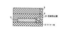
図2に示すように、TEOS−SiO2膜1上に配線3が形成されている。この配線3の上面及び側面に接するように第1の絶縁膜4がTEOS−SiO2膜1全面に形成される。この第1の絶縁膜4上には第2の絶縁膜5が形成される。なお、配線3とTEOS−SiO2膜1間にはライナー材2が形成されており、また、配線3と第1の絶縁膜4の間には反射防止膜21が形成されている。第1の絶縁膜4はヤング率が15GPa以下の材料からなり、第2の絶縁膜5はヤング率が15GPa以上の材料からなる。以下の実施形態においても同様である。
【0070】
本実施形態では、第1の絶縁膜4は有機を含む酸化シリコン膜、第2の絶縁膜5はF添加SiO2膜、TEOS−SiO2膜又はプラズマSiN膜であり、ライナー材2はTi/TiN、配線3はAlである。
【0071】
また、配線3、第1の絶縁膜4及び第2の絶縁膜5の各パラメータが第1実施形態に示した式(2)を満たすように形成される。ここで、第1の絶縁膜4の膜厚dsは、TEOS−SiO2膜1との界面から第2の絶縁膜5との界面までの厚さとする。
【0072】
この半導体装置の製造方法を以下説明する。
【0073】
TEOS−SiO2 膜1上に20nmのTi層及び10nmのTiN層の積層構造からなるライナー材2aを成膜する。続いて配線材料を400nm、5nmのTi層及び60nmのTiN層の積層構造からなる反射防止膜21を成膜する。その後RIEによってパターニングを行い配線3を形成した。
【0074】
次いで、第1の絶縁膜4をパッシベーション膜として成膜する。このとき第1の絶縁膜4の膜厚(図2におけるds)は600nmとする。第1の絶縁膜4の上に、第2の絶縁膜5を形成する。
【0075】
第2の絶縁膜5の膜厚は、F添加SiO2膜の場合は1500nm以下、TEOS−SiO2膜の場合は400nm以下、プラズマSiN膜の場合は100nm以下となるように形成する。
【0076】
なお、以下の実施形態において、配線3,第1及び第2の絶縁膜4,5の積層構造とする理由及び第1の絶縁膜4が15GPa以下で第2の絶縁膜5が15GPa以上とする理由については、第1実施形態と同様であるので省略する。
【0077】
以上のようにして製造される半導体装置について、第2実施形態と同様の条件の下で第2の絶縁膜5の膜厚及び材料を種々変更して実験を行った場合の絶縁膜4及び5の膜厚,s値,MTF,電流密度係数n及びクラック耐性を以下の表3に示す。なお、本発明との比較のため、Al配線上部にTEOS−SiO2(600nm)およびプラズマSiN(600nm)を積層した従来の構造についても、同様に実験を行った。
【0078】
【表3】
配線の膜厚dMは、ライナー材2と配線3と反射防止膜21の膜厚の合計で、495nmとした。MTFについては、TEOS−SiO2/SiN積層構造を第1及び第2の絶縁膜4,5に代えて形成した従来の構造を基準に第1実施形態と同様に判断した。
【0080】
表3に示すように、配線3上に第1の絶縁膜4のみを成膜し、第2の絶縁膜5を形成しない場合には、MTFは従来品よりも著しく向上し、n値も2より大きくなったが、クラックが発生した。第1の絶縁膜4の上に第2の絶縁膜5を10nm成膜することによって、クラックの発生は防止できた。
【0081】
第2の絶縁膜5の膜厚を変化させていくと、s値が5×10⁻⁴より大きい構造では、クラックの発生は起こらなかったが、MTF,n値ともに従来品と同程度であった。s値が5×10⁻⁴以下の配線構造においては、MTFが従来品よりも20%以上向上し、かつnが2より大きな値となった。さらにs値が3.2×10⁻⁴以下の場合には、nは同様に2より大きな値をとり、かつMTFが従来品よりも60%以上向上した。
【0082】
このように、本実施形態によれば、配線の上面及び側面にヤング率が15GPa以下の絶縁膜が接して形成されている構造においても、第1実施形態と同様にクラック耐性、吸水性、透水性の問題を解決しつつ、EM信頼性を向上させることができる。また、第1の絶縁膜4が配線3の側面まで形成されることにより、第1実施形態よりEM信頼性が向上する。
【0083】
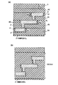
(第3実施形態)
図3(a)は本発明の第3実施形態に係る半導体装置の断面図である。本実施形態では、配線の全面がヤング率15GPa以下の絶縁膜で囲まれている場合について説明する。
【0084】
図3(a)に示すように、熱酸化SiO2膜31上には第1の絶縁膜4が形成されている。この第1の絶縁膜4は層間絶縁膜4a及び4bの積層構造であり、層間絶縁膜4aには溝が形成されており、この溝の底面及び側面を覆うようにライナー材2が形成されている。さらに、このライナー材2を介して溝内に配線3が埋め込み形成されている。また、第1の絶縁膜4上には第2の絶縁膜5が形成されている。さらにこの第2の絶縁膜5上にプラズマSiN膜32が形成されている。第1の絶縁膜4はヤング率が15GPa以下の材料からなり、第2の絶縁膜5はヤング率が15GPa以上の材料からなる。
【0085】
本実施形態では、第1の絶縁膜4は有機を含む酸化シリコン膜、第2の絶縁膜5はF添加SiO2膜又はTEOS−SiO2膜であり、ライナー材2はNb、配線3はAlである。
【0086】
また、配線3、第1の絶縁膜4及び第2の絶縁膜5の各パラメータが第1実施形態に示した式(2)を満たすように形成される。ここで、第1の絶縁膜4の膜厚dsは、熱酸化SiO2膜31との界面から第2の絶縁膜5との界面までの厚さである。
【0087】
この半導体装置の製造方法を以下説明する。
【0088】
まず、図示しない基板上に熱酸化SiO2膜31を作成し、層間絶縁膜4aを800nm成膜し、配線となる溝の加工を行う。溝深さは400nmとする。Nbからなるライナー材2を15nm成膜し、続いてリフロースパッタリングによって配線材料を溝内に成膜する。その後CMPによって溝以外に形成された配線材料を平坦化除去して配線3を形成し、その上面に層間絶縁膜4bを400nm成膜する。層間絶縁膜4a及び4bからなる第1の絶縁膜4の上に第2の絶縁膜5を成膜し、さらにその上面にプラズマSiN膜32を600nm形成する。
【0089】
第2の絶縁膜5の膜厚は、F添加SiO2膜の場合は3000nm以下、TEOS−SiO2膜の場合は800nm以下となるように形成する。
【0090】
以上のようにして製造される半導体装置について、第2実施形態と同様の条件の下で第2の絶縁膜5の膜厚及び材料を種々変更して実験を行った場合の絶縁膜4及び5の膜厚,s値,MTF,電流密度係数n及びクラック耐性を以下の表4に示す。
【0091】
【表4】
なお、本発明との比較のため、TEOS−SiO2/SiN積層膜を層間絶縁膜として用いたAl配線を有する従来の構造についても、同様にEM試験を行った。この比較例の断面図を図3(b)に示す。図3(b)に示すように、本実施形態と異なるのは、第1の絶縁膜4及び第2の絶縁膜5に代えてTEOS−SiO2膜1により層間膜が形成されていることのみである。TEOS−SiO2膜1の膜厚は1600nmである。
【0093】
本実施形態において、第1の絶縁膜4の膜厚dsは、配線3の下部に形成された熱酸化SiO2膜31との界面から、配線3上部の第2の絶縁膜5との界面までの膜厚の合計で、1200nmである。第2の絶縁膜5としては、第1の絶縁膜4の上面に接しているF添加SiO2膜あるいはTEOS−SiO2膜のみであり、最上層のプラズマSiN膜32は、第1の絶縁膜4に直接接しておらず、及ぼす影響が小さいため、第2の絶縁膜5には含まない。
【0094】
MTFについては、図3(b)に示すようなTEOS−SiO2/SiN積層膜を層間絶縁膜として用いた配線を基準として上記実施形態と同様に判断した。配線3上に第1の絶縁膜4のみを成膜した場合には、表4に示したように、MTFは従来品よりも著しく向上し、n値も2より大きくなったが、クラックが発生した。第1の絶縁膜4の上に第2の絶縁膜5を10nm成膜することによって、クラックの発生は防止できた。
【0095】
第2の絶縁膜5の膜厚を変化させていくと、s値が5×10⁻⁴より大きい構造では、クラックの発生は起こらなかったが、MTF,n値ともに従来品と同程度であった。s値が5×10⁻⁴以下の配線構造においては、MTFが従来品よりも20%以上向上し、かつnが2より大きな値となった。さらにs値が3.2×10⁻⁴以下の場合には、nは同様に2より大きな値をとり、かつMTFが従来品よりも60%以上向上した。
【0096】
このように、本実施形態によれば、配線の全面にヤング率が15GPa以下の絶縁膜が囲むように形成されている場合も、第1,2実施形態と同様にクラック耐性、吸水性、透水性の問題を解決しつつ、EM信頼性を向上させることができる。また、第1の絶縁膜4が配線3の側面からさらには下面にまで形成されることにより、第1,2実施形態よりさらにEM信頼性が向上する。
【0097】
(第4実施形態)
図4(a)は本発明の第4実施形態に係る半導体装置の断面図である。本実施形態では、多層配線において配線間には15GPa以下のヤング率をもつ絶縁膜を用い、層間には15GPaより大きいヤング率をもつ絶縁膜を用いる場合について説明する。
【0098】
図4(a)に示すように、TEOS−SiO2膜1上に第1の絶縁膜4が形成されている。第1の絶縁膜4内には、ライナー材2を介して第1の配線41が埋め込み形成されている。この第1の配線41及び第1の絶縁膜4上には第2の絶縁膜5が形成されている。この第2の絶縁膜5上には層間絶縁膜42が形成されており、この層間絶縁膜42には溝が形成されている。さらにこの溝の一部には第2の絶縁膜5を介して第1の配線41に貫通してビアホールが形成されている。このビアホール及び溝には第2の配線43が埋め込み形成されている。この第2の配線43は、上面を除いてライナー材2が形成されており、第2の配線43及び第2の絶縁膜5上にはTEOS−SiO2膜1が形成されている。さらにこのTEOS−SiO2膜1上にはプラズマSiN膜32が形成されている。
【0099】
また、配線41、第1の絶縁膜4及び第2の絶縁膜5の各パラメータが第1実施形態に示した式(2)を満たすように形成される。
【0100】
この半導体装置の製造方法を以下説明する。
【0101】
まず、TEOS−SiO2膜1上に形成された第1の絶縁膜4に溝を形成し、この溝にライナー材2を介して第1の配線41をダマシンプロセスにより埋め込み形成する。次いで、この第1の配線41及び第1の絶縁膜4上に第2の絶縁膜5及び層間絶縁膜42を積層して形成する。そして、RIE等により層間絶縁膜42及び第2の絶縁膜5を選択的に除去して第1の配線41まで貫通するビアホールを設けた後、このビアホールの設けられた領域を含めて層間絶縁膜42を選択的に除去して溝を形成する。次いで、ビアホールを含めて溝表面を覆うようにライナー材2を形成し、さらにこの溝内にデュアルダマシンプロセスにより第2の配線43を埋め込み形成する。
【0102】
本実施形態では、第1及び第2の配線41,43ともにAlにより形成され、第1の絶縁膜4には有機を含む酸化シリコン膜(300nm)を、第2の絶縁膜5にはF添加SiO2膜、TEOS−SiO2膜又はプラズマSiN膜のいずれかが用いられる。また、第2の配線43上部にパッシベーション膜として形成されるTEOS−SiO2膜1及びプラズマSiN32はそれぞれ600nmの膜厚である。第2の絶縁膜5の膜厚は、F添加SiO2膜の場合は800nm以下、TEOS−SiO2膜の場合は200nm以下、プラズマSiN膜の場合は50nm以下となるように形成する。
【0103】
以上のようにして製造される半導体装置について、第2の絶縁膜5の膜厚及び材料を種々変更して実験を行った場合の絶縁膜4及び5の膜厚,s値,MTF,電流密度係数n及びクラック耐性を以下の表5に示す。
【0104】
【表5】
なお、本発明との比較のため、TEOS−SiO2 膜1を全ての層間絶縁膜として用いたAl配線を有する従来の構造についても、同様にEM試験を行った。この比較例の断面図を図4(b)に示す。図4(b)に示すように、本実施形態と異なるのは、第1の絶縁膜4,第2の絶縁膜5,層間絶縁膜42からなる膜に代えてTEOS−SiO2膜1により層間膜が形成されていることのみである。
【0106】
配線膜厚dMには第1の配線41の膜厚(300nm)を、15GPa以下のヤング率をもつ第1の絶縁膜4の膜厚dsは、第1の配線41の配線間の有機を含む酸化シリコン膜の膜厚(300nm)とする。第2の絶縁膜5の膜厚dhとしては、第1及び第2の配線41,43の層間のF添加SiO2膜,TEOS−SiO2膜又はプラズマSiN膜のいずれかの膜厚とする。
【0107】
MTFについては、図4(b)に示すようなTEOS−SiO2/SiN積層膜を層間絶縁膜として用いた場合を基準として判断した。
【0108】
配線41上に有機を含む酸化シリコン膜のみを成膜した場合には、表5に示したように、MTFは従来品よりも著しく向上し、n値も2より大きくなったが、クラックが発生した。第1の絶縁膜4上に第2の絶縁膜5を10nm成膜することによって、クラックの発生は防止できた。第2の絶縁膜5の膜厚を変化させていくと、s値が5×10⁻⁴より大きい構造では、クラックの発生は起こらなかったが、MTF,n値ともに従来品と同程度であった。s値が5×10⁻⁴以下の配線構造においては、MTFが従来品よりも20%以上向上し、かつnが2より大きな値となった。さらにs値が3.2×10⁻⁴以下の場合には、nは同様に2より大きな値をとり、かつMTFが従来品よりも60%以上向上した。
【0109】
(第5実施形態)
図5(a)は本発明の第5実施形態に係る半導体装置の断面図である。本実施形態では、多層配線において配線間、層間ともに同一の15GPa以下のヤング率を持つ絶縁膜を用いる場合について説明する。
【0110】
図5(a)に示すように、熱酸化SiO2膜31上に層間絶縁膜4aが形成され、この層間絶縁膜4a内に所定の深さの溝が形成されている。この溝内にはライナー材2を介して第1の配線41が埋め込み形成されている。この第1の配線41及び層間絶縁膜4a上には層間絶縁膜4bが形成され、この層間絶縁膜4bに所定の深さの溝と、第1の配線41に貫通するビアホールが形成されている。この溝及びビアホールには、ライナー材2を介して第2の配線43が埋め込み形成されている。
【0111】
第2の配線43及び層間絶縁膜4b上には層間絶縁膜4cが形成されており、この層間絶縁膜4cに所定の深さの溝と、第2の配線43に貫通するビアホールが形成されている。この溝及びビアホールには、第3の配線51が形成されている。さらにこの第3の配線41及び層間絶縁膜4cの上には、層間絶縁膜4dを介してパッシベーション膜として第2の絶縁膜5が形成されている。なお、層間絶縁膜4a〜4dまでを含めて第1の絶縁膜4とする。第1〜第3の配線41,43及び44の膜厚は全て400nmである。
【0112】
また、配線3、第1の絶縁膜4及び第2の絶縁膜5の各パラメータが第1実施形態に示した式(2)を満たすように形成される。
【0113】
この半導体装置の製造方法を以下説明する。なお、第4実施形態と共通する部分についての詳細な説明は省略する。本実施形態では、第1の配線41にはAlダマシン配線が用られ、ビアおよび第2、第3の配線43,51は、デュアルダマシンプロセスで作成する。
【0114】
層間絶縁膜4a〜4dにより構成される第1の絶縁膜4は、すべて第1実施形態記載の有機を含む酸化シリコン膜が用いられる。第1の絶縁膜4の合計の膜厚は2800nmである。第2の絶縁膜5にはプラズマSiN膜であり、その膜厚は800nm以下となるように形成する。
【0115】
以上のようにして製造される半導体装置について、上記実施形態と同様の条件の下で第2の絶縁膜5の膜厚を種々変更して実験を行った場合の絶縁膜4及び5の膜厚,s値,MTF,電流密度係数n及びクラック耐性を以下の表6に示す。
【0116】
【表6】
本実施形態の半導体装置のうち、第1〜第3の配線41,43及び51の各配線を試験配線としてEM試験を行った。
【0118】
なお、本発明との比較のため、TEOS−SiO2を全ての層間絶縁膜として用いたAl配線を有する従来の構造についても、同様にEM試験を行った。この比較例の断面図を図5(b)に示す。図5(b)に示すように、本実施形態と異なるのは、第1の絶縁膜4に代えてTEOS−SiO2膜1により層間膜が形成されていることのみである。TEOS−SiO2膜1の膜厚は2800nmである。
【0119】
配線膜厚dMには第1〜第3の配線41,43及び51の合計膜厚(1200nm)を、15GPa以下のヤング率をもつ第1の絶縁膜4の膜厚dsは、層間絶縁膜4a〜4dの合計膜厚(2800nm)とする。第2の絶縁膜5の膜厚dhは、プラズマSiN膜の膜厚とする。MTFについては、図5(b)に示すようなTEOS−SiO2/SiN積層膜を層間絶縁膜として用いた半導体装置を基準として判断した。
【0120】
第1の絶縁膜4のみを成膜した場合には、表5に示すように、MTFは従来品よりも著しく向上し、n値も2より大きくなったが、クラックが発生した。第2の絶縁膜5を第1の絶縁膜4の上に10nm成膜することによって、クラックの発生は防止できた。第2の絶縁膜5の膜厚を変化させていくと、s値が5×10⁻⁴より大きい構造では、クラックの発生は起こらなかったが、MTF,n値ともに従来品と同程度であった。s値が5×10⁻⁴以下の配線構造においては、MTFが従来品よりも20%以上向上し、かつnが2より大きな値となった。さらにs値が3.2×10⁻⁴以下の場合には、nは同様に2より大きな値をとり、かつMTFが従来品よりも60%以上向上した。
【0121】
第2層配線、第3層配線を試験配線として実験した場合にも同様の結果が得られた。
【0122】
(第6実施形態)
図6(a)は本発明の第6実施形態に係る半導体装置の断面図である。本実施形態では、多層配線において配線間と層間に用いられる絶縁膜は異なる材料であるが、ともに15GPa以下のヤング率をもつ場合について説明する。
【0123】
図6(a)に示すように、熱酸化SiO2膜31上に層間絶縁膜61及び62が積層して形成されている。層間絶縁膜62には溝が形成されており、この溝には第1の配線41が埋め込み形成されている。第1の配線41及び層間絶縁膜62上には層間絶縁膜63及び64が積層して形成されている。層間絶縁膜63及び64を貫通して第1の配線41に達するビアホールが形成されており、さらに層間絶縁膜64にはこのビアホールを含む領域に溝が形成されている。このビアホールを含めて溝内には第2の配線43が埋め込み形成されている。第2の配線43及び層間絶縁膜64の上には層間絶縁膜65及びパッシベーション膜として第2の絶縁膜5が積層して形成されている。なお、第1及び第2の配線の底面及び側面には、ライナー材2が形成されている。また、本実施形態では層間絶縁膜61〜65を第1の絶縁膜4とする。
【0124】
第1及び第2の配線41,42ともに膜厚は300nmである。配線41,42の側部に設けられた層間絶縁膜62,64にはそれぞれ300nmの膜厚の有機を含む酸化シリコン膜を、層間絶縁膜61,63及び65には、それぞれ400nmの膜厚のポリイミド膜が用いられる。また、第2の絶縁膜5にはプラズマSiN膜が用いられる。
【0125】
また、配線41、第1の絶縁膜4及び第2の絶縁膜5の各パラメータが第1実施形態に示した式(2)を満たすように形成される。
【0126】
なお、この半導体装置は、第1の配線41はAlダマシン配線を用い、ビアおよび第2の配線43は、デュアルダマシンプロセスで作成する。第2の絶縁膜5の膜厚は500nm以下となるように形成する。他の製造方法は上記実施形態と共通するので説明は省略する。
【0127】
以上のようにして製造される半導体装置について、上記実施形態と同様の条件の下で第2の絶縁膜5の膜厚を種々変更して実験を行った場合の絶縁膜4及び5の膜厚,s値,MTF,電流密度係数n及びクラック耐性を以下の表7に示す。
【0128】
【表7】
本実施形態の半導体装置のうち、第1及び第2の配線41及び43の各配線を試験配線としてEM試験を行った。
【0130】
なお、本発明との比較のため、TEOS−SiO2を全ての層間絶縁膜として用いたAl配線を有する従来の構造についても、同様にEM試験を行った。この比較例の断面図を図6(b)に示す。図6(b)に示すように、本実施形態と異なるのは、第1の絶縁膜4に代えてTEOS−SiO2膜1により層間膜が形成されていることのみである。TEOS−SiO2膜1の膜厚は1800nmである。
【0131】
配線膜厚dMには第1及び第2の配線41,43の合計膜厚(600nm)を用いる。15GPa以下のヤング率をもつ第1の絶縁膜4の合計膜厚ds、複合されたヤング率Es及び線膨張係数αsは、次式で定義される。
【0132】
ds=ds1+ds2+ ds3+ ds4+ds5
Es=(ds1Es1+ds2Es2+ds3Es1+ds4Es2+ds5Es1)/ds
αs1=(ds1αs1+ds1αs1+ds1αs1+ds1αs1+ds1αs1)/ds
なお、ds1〜ds5は,Es1〜Es5及びαs1〜αs5はそれぞれ順に層間絶縁膜61〜65の膜厚,ヤング率及び線膨張係数を示す。本実施形態で用いるポリイミド膜のヤング率は5.2GPa、線膨張係数は10-5である。
【0133】
上式から、ds=1800nm,Es=5.5GPa,αs=10-5である。第2絶縁膜の膜厚dhは、プラズマSiN膜の膜厚とした。MTFについては、図6(b)に示すようなTEOS−SiO2/SiN積層膜を層間絶縁膜として用いた配線を基準として判断した。
【0134】
配線上に第1の絶縁膜4のみを成膜した場合には、表7に示したように、MTFは従来品よりも著しく向上し、n値も2より大きくなったが、クラックが発生した。第1の絶縁膜4上に第2の絶縁膜5を10nm成膜することによって、クラックの発生は防止できた。第2の絶縁膜5の膜厚を変化させていくと、s値が5×10⁻⁴より大きい構造では、クラックの発生は起こらなかったが、MTF,n値ともに従来品と同程度であった。s値が5×10⁻⁴以下の配線構造においては、MTFが従来品よりも20%以上向上し、かつnが2より大きな値となった。さらにs値が3.2×10⁻⁴以下の場合には、nは同様に2より大きな値をとり、かつMTFが従来品よりも60%以上向上した。
【0135】
第2の配線43を試験配線とした場合にも同様の結果が得られた。
【0136】
(第7実施形態)
第7の実施形態として、配線材料がCu又はCu合金である場合について説明する。
【0137】
表8に第1実施形態記載の構造におけるAl配線をCu配線に置換した半導体装置について実験を行った場合の絶縁膜4及び5の膜厚,s値,MTF,電流密度係数n及びクラック耐性を以下の表8に示す。
【0138】
【表8】
測定結果からCu配線の場合は、k1=1.2,k2=10-3であった。ライナー材および配線上部のバリアメタルとしては、TiN又TaNを用いた。配線の膜厚dMは、ライナー材と配線上面のバリア層およびCuの膜厚の合計で、400nmである。配線材料のヤング率(EM)および線膨張係数(αM)は、Cuの物性値(EM=126GPa,αM=1.7×10⁻⁵)を用いた。MTFについては、TEOS−SiO2 /SiN積層膜を層間絶縁膜として用いた配線を基準として判断した。
【0140】
表8に示すように、第1の絶縁膜4のみを成膜した場合には、MTFは従来品よりも著しく向上し、n値も2より大きくなったが、クラックが発生した。第1の絶縁膜4上に第2の絶縁膜5を10nm成膜することによって、クラックの発生は防止できた。第2の絶縁膜5の膜厚を変化させていくと、s値が5×10⁻⁴より大きい構造では、クラックの発生は起こらなかったが、MTF,n値ともに従来品と同程度であった。s値が5×10⁻⁴以下の配線構造においては、MTFが従来品よりも20%以上向上し、かつnが2より大きな値となった。さらにs値が3.2×10⁻⁴以下の場合には、nは同様に2より大きな値をとり、かつMTFが従来品よりも60%以上向上した。
【0141】
以上より、第2の絶縁膜5の膜厚は、F添加SiO2膜の場合は1500nm以下、TEOS−SiO2膜の場合は300nm以下、プラズマSiN膜の場合は100nm以下に定まる。
【0142】
また、第2〜第6実施形態全ての構造において、配線材料がCu又はCu合金の場合でもAl配線の場合と同様の効果が得られた。Cu配線の場合には、配線とそれに接する絶縁膜との間にバリア層が存在するが、s値を計算する際にこのバリア層の膜厚は、バリア層が導電膜の場合には配線膜厚に、バリア層が絶縁物の場合には絶縁膜の膜厚に加えた。
【0143】
本発明は上記実施形態に限定されるものではない。
【0144】
また、膜の形成方法としては、スピンコート以外にCVD法、蒸着重合、スパッタリング法などを用いて作製した有機を含む酸化シリコン膜についても同様の効果が得られる。また有機を含む酸化シリコン膜は、添加物としてTi、ジルコニア又はAlの金属酸化物を含んでいても構わない。
【0145】
ライナー材については、Nb以外にTi,TiN,Ta又はTaAlなどを用いた場合にも同様の効果が得られた。
【0146】
【発明の効果】
以上詳述したように本発明によれば、配線に接するように第1の絶縁膜が形成され、さらにこの第1の絶縁膜上に接して該第1の絶縁膜よりもヤング率の低い第2の絶縁膜が形成された構造とし、配線に働く応力の温度勾配s<5×10⁻⁴となるように各パラメータを適切に定めることにより、配線のクラック耐性を保持しつつEM信頼性が著しく向上する。
【図面の簡単な説明】
【図1】本発明の第1実施形態に係る半導体装置の断面図。
【図2】本発明の第2実施形態に係る半導体装置の断面図。
【図3】本発明の第3実施形態に係る半導体装置の断面図。
【図4】本発明の第4実施形態に係る半導体装置の断面図。
【図5】本発明の第5実施形態に係る半導体装置の断面図。
【図6】本発明の第6実施形態に係る半導体装置の断面図。
【符号の説明】
1…TEOS−SiO2膜
2…ライナー材
3…配線
4…第1の絶縁膜
4a〜4d,42,61〜65…層間絶縁膜
5…第2の絶縁膜
21…反射防止膜
31…熱酸化SiO2膜
32…プラズマSiN膜
41…第1の配線
43…第2の配線
51…第3の配線[0001]
BACKGROUND OF THE INVENTION
The present invention relates to a semiconductor device having a multilayer structure of LSI, and more particularly to a semiconductor device having a multilayer structure for increasing the reliability of wiring.
[0002]
[Prior art]
The electromigration (hereinafter referred to as EM) defect, which has the biggest problem with LSI wiring, occurs with the following mechanism. Metal atoms forming the wiring move from the cathode (−) to the anode (+) side, and at that time, tensile stress accumulates with a decrease in the density of metal atoms on the cathode side of the wiring. When this tensile stress exceeds the critical stress, voids are generated and breakage occurs.
[0003]
If the insulating film surrounding the wiring can be deformed by receiving stress from the wiring, the stress of the wiring is relieved and EM defects are less likely to occur. However, plasma SiO, which has been used as an interlayer insulating film in conventional semiconductor devices2The Young's modulus of the film and the plasma SiN film are both relatively high at 50 GPa or more. These films hardly deform even under stress. Therefore, the conventional semiconductor device has low EM resistance.
[0004]
In some conventional semiconductor devices, an insulating film having a low Young's modulus is formed in contact with the wiring. In this case, problems such as crack resistance, water absorption, and water permeability occur.
[0005]
[Problems to be solved by the invention]
As described above, in the conventional semiconductor device, since the Young's modulus of the insulating film formed in contact with the wiring is high, the insulating film hardly deforms when subjected to stress, so that the EM resistance is low. Further, a semiconductor device having high EM resistance due to a structure in which an insulating film having a low Young's modulus is formed in contact with the wiring may be considered, but problems of crack resistance, water absorption, and water permeability occur.
[0006]
The present invention has been made to solve the above-described problems, and an object of the present invention is to provide a semiconductor device that improves EM resistance while maintaining crack resistance.
[0007]
[Means for Solving the Problems]
According to a first aspect of the present invention, there is provided a wiring, a first insulating film formed in contact with at least one surface of the wiring, and the first insulating film formed in contact with the first insulating film. A semiconductor device comprising a second insulating film having a higher Young's modulus than the film, wherein the linear expansion coefficient of each of the wiring, the first insulating film, and the second insulating film is expressed as αM, Αs, ΑhAnd each Young's modulus is EM, Es, EhAnd each film thickness is dM, Ds, DhAnd the coefficient determined by the material constituting the wiring is k1, K2And dI= Ds+ Dh, EI= (DsEs+ DhEh) / DI, ΑI= (Dsαs+ Dhαh) / DIWhen the temperature gradient of stress acting on the wiring is defined as s, the wiring, the first insulating film, and the second insulating film are:
[0008]
[Equation 8]
It satisfies the following conditions.
[0010]
Desirable embodiments of the present invention are shown below.
[0011]
(1) The first insulating film is made of a material having a Young's modulus of 15 GPa or less, and the second insulating film is made of a material having a Young's modulus of 15 GPa or more.
[0012]
(2) The first insulating film is a laminated film made of different materials, and the film thickness of the i-th insulating film counted from the wiring side is ds i, Young's modulus Es i, Αs iThen,
[0013]
[Equation 9]
It is represented by
[0015]
(3) The first film includes at least one film containing silicon oxide containing an organic material as a main component.
[0016]
(4) The organic material has a methyl group as a main component.
[0017]
(5) When the material of the wiring is Al or its alloy, the coefficient k1Is 1 and the coefficient k2Value of 10-3It is.
[0018]
(6) When the material of the wiring is Cu or an alloy thereof, the coefficient k1Is 1.2 and the coefficient k2Value of 10-3It is.
[0019]
(7) The first and second insulating films are formed so as to surround the wiring.
[0020]
(Function)
The current density coefficient n, which is known as one of the parameters of electromigration (hereinafter referred to as EM) reliability, is an index representing the reliability of EM, like MTF (Means Time to Failure) and activation energy. Yes, the greater the n value, the higher the reliability of the EM. In the conventional semiconductor device, when there is only one insulating film formed in contact with the wiring, and it is considered that the insulating film does not deform due to the stress received from the wiring, until the resistance rises by EM The n value obtained from the time (incubation time) is ideally set to 2 and never takes a value larger than 2.
[0021]
On the other hand, the temperature gradient s of stress acting on the wiring is presumed that the smaller the value, the greater the stress relaxation effect due to the deformation of the insulating film. The same effect is shown.
[0022]
When the wiring is surrounded by an insulating film, the temperature gradient of the stress acting on the wiring is usually expressed by the following equation.
[0023]
s = dσ / dT = EM・ (ΑM-ΑI)
However, this expression is an expression when the insulating film is not deformed by the stress received from the wiring. TEOS-SiO used as interlayer insulation film2Films, SiN films, and the like have a large Young's modulus of 50 GPa or more and a linear expansion coefficient of 1/10 or less of Al. Therefore, the amount of deformation of the insulating film due to the stress received from the wiring is negligibly small.
[0024]
However, when an insulating film having a small Young's modulus of 15 GPa or less is used around the wiring, it is assumed that the insulating film is deformed by the stress received from the wiring, and the stress of the wiring is relieved by this deformation. When the temperature gradient of the stress of the wiring is derived under the condition of deformation, the following equation (1) is obtained.
[0025]
[Expression 10]
EIIs the Young's modulus of the material constituting the interlayer insulating film, dMIs the thickness of the wiring, dIIs the thickness of the interlayer insulating film, k1, K2Represents a coefficient determined by the wiring material.
[0027]
When the wiring stress gradient represented by the expression (1) is s, it is estimated that the smaller the s value, the greater the effect of stress relaxation due to the deformation of the insulating film. This stress relaxation effect shows not only the thermal stress but also the same effect on the stress generated in the wiring by EM.
[0028]
Furthermore, when the insulating film has a laminated structure, the effective Young's modulus and effective linear expansion coefficient of the insulating film can be expressed by the following three formulas according to the composite rule.
[0029]
dI= Ds+ Dh
EI= (DsEs+ DhEh) / DI
αI= (Dsαs+ Dhαh) / DI
The value of s when the insulating film has a laminated structure can be derived by introducing the above three formulas into formula (1).
[0030]
Here, when the current density coefficient n, which is a condition for improving the reliability of the EM described above, is 2, s ≧ 5 × 10 5 based on empirical rules based on various experiments.-FourIt becomes. Therefore, in order to improve the reliability of EM, the s value shown in the above equation (1) is 5 × 10 5.-FourIt is necessary that:
[0031]
Here, even when there is only one insulating film formed in contact with the wiring and the deformation of the insulating film due to the stress received from the wiring is taken into consideration, the n value takes a value larger than 2. However, in this case, there is a problem that cracks occur.
[0032]
Therefore s <5 × 10-FourIn addition to selecting materials and film thicknesses that satisfy the above conditions, in order to solve the problems of crack resistance, water absorption, and water permeability, an insulating film made of a material having a low Young's modulus is in contact with the wiring. In addition, it is necessary to form an insulating film made of a material having a high Young's modulus in contact with the insulating film having a low Young's modulus.
[0033]
As described above, a semiconductor device that solves the problems of sufficient EM reliability, crack resistance, water absorption, and water permeability has a laminated structure of wiring and first and second insulating films having different Young's moduli. Is s <5 × 10-FourIt has a material and a film thickness that satisfy the following conditions.
[0034]
Accordingly, a first insulating film is formed on at least one surface of the wiring as in the present invention, and a second insulating film having a higher Young's modulus than the first insulating film is further in contact with the first insulating film. And each of these layers is s <5 × 10-FourBy setting the material and film thickness to satisfy the above conditions, the EM reliability is improved as compared with the conventional semiconductor device while solving problems such as crack resistance, water absorption and water permeability.
[0035]
DETAILED DESCRIPTION OF THE INVENTION
Hereinafter, embodiments of the present invention will be described with reference to the drawings.
[0036]
(First embodiment)
FIG. 1 is a sectional view of a semiconductor device according to the first embodiment of the present invention. In this embodiment, a case where an insulating film having a Young's modulus of 15 GPa or less is formed in contact with the upper surface of the wiring will be described.
[0037]
As shown in FIG. 1, TEOS-SiO2A groove having a depth of 400 nm is formed in the
[0038]
In the present embodiment, the first insulating
[0039]
The film thickness of each of the
[0040]
## EQU11 ##
In the above formula (2), dI= Ds+ Dh, EI= (DsEs+ DhEh) / DI, ΑI= (Dsαs+ Dhαh) / DIAnd k1And k2Is a coefficient determined by the wiring material. This k1And k2Is a coefficient introduced in order to uniquely define the conditions in the above equation (2) even when different wiring materials are used, and can be derived by conducting an experiment for each wiring material.
[0042]
A method for manufacturing this semiconductor device will be described below.
[0043]
First, as an interlayer insulating film, TEOS-SiO2Film 1 is formed and this TEOS-SiO2A groove having a depth of 400 nm is processed in the
[0044]
The Young's modulus of the material used for this semiconductor device is 6 GPa for the silicon oxide film containing organic, and F-added SiO.2The film is 36 GPa, TEOS-SiO2The film shows 57 GPa and the plasma SiN film shows 98 GPa. These Young's moduli are values measured using an indentation hardness meter.
[0045]
The thickness of the second
[0046]
The reason for limiting the film thickness of the second
[0047]
The current density coefficient n, which is known as one of the parameters of electromigration (hereinafter referred to as EM) reliability, is an index representing the reliability of EM, like MTF (Means Time to Failure) and activation energy. Yes, the greater the n value, the higher the reliability of the EM. In the conventional semiconductor device, when there is only one insulating film formed in contact with the wiring, and it is considered that the insulating film does not deform due to the stress received from the wiring, until the resistance increase starts to occur due to EM The n value obtained from the time (incubation time) is ideally set to 2 and never takes a value larger than 2. Accordingly, when the n value is 2 or more, the reliability of the EM is improved as compared with the case where the insulating film is a single layer and is not deformed by stress.
[0048]
On the other hand, the temperature gradient s of stress acting on the wiring is presumed that the smaller the value, the greater the stress relaxation effect due to the deformation of the insulating film. The same effect is shown. Here, when satisfying n = 2, which is a condition for improving the reliability of the EM, s ≧ 5 × 10 5 based on empirical rules based on various experiments.-FourIt becomes. Therefore, in order to improve the reliability of EM, the s value shown in the above equation (2) is 5 × 10 5.-FourIt is necessary that:
[0049]
Here, even when there is only one insulating film formed in contact with the wiring and the deformation of the insulating film due to the stress received from the wiring is taken into consideration, the n value takes a value larger than 2. However, in this case, there is a problem that cracks occur.
[0050]
Therefore s <5 × 10-FourIn addition to selecting a material and film thickness that satisfy the above conditions, an insulating film made of a material with a low Young's modulus is in contact with the wiring in order to create a structure that does not generate crack resistance, water absorption, and water permeability. In addition, it is necessary to form an insulating film made of a material having a high Young's modulus in contact with the insulating film having a low Young's modulus.
[0051]
As described above, a semiconductor device that has sufficient EM reliability and solves the problems of crack resistance, water absorption, and water permeability has a laminated structure of wiring and first and second insulating films having different Young's moduli. Each of these layers is s <5 × 10-FourIt has a material and a film thickness that satisfy the following conditions.
[0052]
In the case of this embodiment, when the material and film thickness of the
[0053]
Next, the following table shows the film thickness, s value, MTF, current density coefficient n, and crack resistance of the insulating
[0054]
[Table 1]
In Table 1, for comparison with the present invention, as an example of a conventional structure in which both the first insulating film and the second insulating film are films that do not deform due to stress received from the wiring, Replaced with the second insulating
[0056]
The wiring material is Al and EM= 80 GPa, dM= 400 nm, αM= 2.4 × 10-FiveWas used. From the measurement results, when the wiring is Al, k1= 1, k2= 10 × 10-3Met. The linear expansion coefficient of each insulating film was obtained by measuring the temperature change of the warp using a wafer warp measuring device. Linear expansion coefficient of organic silicon oxide film (αs) Is 10-Five, F-added SiO2Film, TEOS-SiO2Coefficient of linear expansion of the film or plasma SiN film (αh) Are all 7x10⁻⁶It was. Further, the film thickness d of the
[0057]
In addition, the EM average life (MTF) under the acceleration condition of the conventional structure shown as a comparative example is 75 hours, and a column for comparison with this MTF is provided in Table 1 under the same acceleration condition as in the present invention. In the case where the MTF is less than 90 hours, it is the same as that of the conventional product.
[0058]
In addition, in the conventional insulating film having a large Young's modulus, the current density coefficient n does not cause deformation of the insulating film in contact with the wiring during EM. Under such conditions, n = 2 and is larger than 2. There was no. On the other hand, n takes a value larger than 2 under the condition that the insulating film is deformed by the stress received from the wiring as in the wiring structure of the present embodiment. When only the first insulating
[0059]
Thus, the film thickness of the second
[0060]
Next, the reason why the first insulating
[0061]
Table 2 shows the s-value, MTF, current density coefficient n, and crack resistance when the experiment was performed with various changes in the Young's modulus of the first insulating
[0062]
[Table 2]
In the experiment shown in Table 2, after the
[0064]
On the first insulating
[0065]
When the Young's modulus of the first insulating
[0066]
From the above, it can be seen that the first insulating
[0067]
As the first insulating
[0068]
(Second Embodiment)
FIG. 2 is a sectional view of a semiconductor device according to the second embodiment of the present invention. In the present embodiment, a case where an insulating film having a Young's modulus of 15 GPa or less is formed in contact with the upper surface and side surfaces of the wiring will be described. In the following embodiments, common components are denoted by the same reference numerals, and detailed description thereof is omitted.
[0069]
As shown in FIG. 2, TEOS-SiO2A wiring 3 is formed on the
[0070]
In the present embodiment, the first insulating
[0071]
The parameters of the
[0072]
A method for manufacturing this semiconductor device will be described below.
[0073]
TEOS-SiO2A liner material 2 a having a laminated structure of a 20 nm Ti layer and a 10 nm TiN layer is formed on the
[0074]
Next, the first insulating
[0075]
The thickness of the second
[0076]
In the following embodiment, the reason why the
[0077]
With respect to the semiconductor device manufactured as described above, the insulating
[0078]
[Table 3]
Wiring thickness dMThe total thickness of the
[0080]
As shown in Table 3, when only the first insulating
[0081]
When the thickness of the second
[0082]
As described above, according to the present embodiment, even in the structure in which the insulating film having a Young's modulus of 15 GPa or less is in contact with the upper surface and the side surface of the wiring, crack resistance, water absorption, water permeability are the same as in the first embodiment. EM reliability can be improved while solving the problem of safety. Further, since the first insulating
[0083]
(Third embodiment)
FIG. 3A is a sectional view of a semiconductor device according to the third embodiment of the present invention. In the present embodiment, a case where the entire surface of the wiring is surrounded by an insulating film having a Young's modulus of 15 GPa or less will be described.
[0084]
As shown in FIG. 3 (a), thermally oxidized SiO2A first insulating
[0085]
In the present embodiment, the first insulating
[0086]
The parameters of the
[0087]
A method for manufacturing this semiconductor device will be described below.
[0088]
First, thermally oxidized SiO2 is formed on a substrate (not shown).2A
[0089]
The thickness of the second
[0090]
With respect to the semiconductor device manufactured as described above, the insulating
[0091]
[Table 4]
For comparison with the present invention, TEOS-SiO2Similarly, an EM test was performed on a conventional structure having an Al wiring using a / SiN laminated film as an interlayer insulating film. A cross-sectional view of this comparative example is shown in FIG. As shown in FIG. 3B, the present embodiment differs from the present embodiment in that TEOS-SiO instead of the first insulating
[0093]
In the present embodiment, the film thickness d of the first insulating
[0094]
For MTF, TEOS-SiO as shown in FIG.2The determination was made in the same manner as in the above embodiment, with reference to the wiring using the / SiN laminated film as the interlayer insulating film. When only the first insulating
[0095]
When the thickness of the second
[0096]
Thus, according to the present embodiment, even when an insulating film having a Young's modulus of 15 GPa or less is surrounded on the entire surface of the wiring, crack resistance, water absorption, water permeability are the same as in the first and second embodiments. EM reliability can be improved while solving the problem of safety. Further, since the first insulating
[0097]
(Fourth embodiment)
FIG. 4A is a cross-sectional view of a semiconductor device according to the fourth embodiment of the present invention. In this embodiment, a case where an insulating film having a Young's modulus of 15 GPa or less is used between the wirings in a multilayer wiring and an insulating film having a Young's modulus greater than 15 GPa is used between the layers will be described.
[0098]
As shown in FIG. 4 (a), TEOS-SiO2A first insulating
[0099]
The parameters of the
[0100]
A method for manufacturing this semiconductor device will be described below.
[0101]
First, TEOS-SiO2A groove is formed in the first insulating
[0102]
In this embodiment, the first and
[0103]
Regarding the semiconductor device manufactured as described above, the thickness, s value, MTF, and current density of the insulating
[0104]
[Table 5]
For comparison with the present invention, TEOS-SiO2An EM test was similarly performed on a conventional structure having an Al wiring using the
[0106]
Wiring thickness dMThe thickness (300 nm) of the
[0107]
For MTF, TEOS-SiO as shown in FIG.2The determination was made based on the case where the / SiN laminated film was used as an interlayer insulating film.
[0108]
When only an organic silicon oxide film was formed on the
[0109]
(Fifth embodiment)
FIG. 5A is a sectional view of a semiconductor device according to the fifth embodiment of the present invention. In the present embodiment, a case where an insulating film having the same Young's modulus of 15 GPa or less is used between the wirings and between the layers in the multilayer wiring will be described.
[0110]
As shown in FIG. 5 (a), thermally oxidized SiO2An interlayer insulating
[0111]
An interlayer insulating film 4c is formed on the
[0112]
The parameters of the
[0113]
A method for manufacturing this semiconductor device will be described below. Note that a detailed description of parts common to the fourth embodiment is omitted. In the present embodiment, Al damascene wiring is used for the
[0114]
As the first insulating
[0115]
Regarding the semiconductor device manufactured as described above, the film thicknesses of the insulating
[0116]
[Table 6]
In the semiconductor device of this embodiment, the EM test was performed using each of the first to
[0118]
For comparison with the present invention, TEOS-SiO2Similarly, the EM test was conducted on the conventional structure having Al wirings using all of the above as an interlayer insulating film. A cross-sectional view of this comparative example is shown in FIG. As shown in FIG. 5B, the present embodiment differs from the present embodiment in that TEOS-SiO instead of the first insulating
[0119]
Wiring thickness dMThe total film thickness (1200 nm) of the first to
[0120]
When only the first insulating
[0121]
Similar results were obtained when the second layer wiring and the third layer wiring were tested as test wirings.
[0122]
(Sixth embodiment)
FIG. 6A is a sectional view of a semiconductor device according to the sixth embodiment of the present invention. In this embodiment, the insulating films used between the wirings and between the layers in the multilayer wiring are made of different materials, but a case where both have Young's modulus of 15 GPa or less will be described.
[0123]
As shown in FIG. 6 (a), thermally oxidized SiO2
[0124]
The film thickness of both the first and
[0125]
The parameters of the
[0126]
In this semiconductor device, the
[0127]
Regarding the semiconductor device manufactured as described above, the film thicknesses of the insulating
[0128]
[Table 7]
In the semiconductor device of this embodiment, the EM test was performed using each of the first and
[0130]
For comparison with the present invention, TEOS-SiO2Similarly, the EM test was conducted on the conventional structure having Al wirings using all of the above as an interlayer insulating film. A cross-sectional view of this comparative example is shown in FIG. As shown in FIG. 6B, the present embodiment differs from the present embodiment in that TEOS-SiO instead of the first insulating
[0131]
Wiring thickness dMFor this, the total film thickness (600 nm) of the first and
[0132]
ds= Ds1+ Ds2+ Ds3+ Ds4+ Ds5
Es= (Ds1Es1+ Ds2Es2+ Ds3Es1+ Ds4Es2+ Ds5Es1) / Ds
αs1= (Ds1αs1+ Ds1αs1+ Ds1αs1+ Ds1αs1+ Ds1αs1) / Ds
Ds1~ Ds5Is Es1~ Es5And αs1~ Αs5Indicates the film thickness, Young's modulus, and linear expansion coefficient of the interlayer insulating
[0133]
From the above equation, ds= 1800 nm, Es= 5.5 GPa, αs= 10-FiveIt is. Film thickness d of the second insulating filmhIs the thickness of the plasma SiN film. For MTF, TEOS-SiO as shown in FIG.2The determination was made based on the wiring using the / SiN laminated film as the interlayer insulating film.
[0134]
When only the first insulating
[0135]
Similar results were obtained when the
[0136]
(Seventh embodiment)
A case where the wiring material is Cu or a Cu alloy will be described as a seventh embodiment.
[0137]
Table 8 shows the film thickness, s value, MTF, current density coefficient n, and crack resistance of the insulating
[0138]
[Table 8]
In the case of Cu wiring from the measurement result, k1= 1.2, k2= 10-3Met. TiN or TaN was used as the liner material and the barrier metal above the wiring. Wiring thickness dMIs 400 nm in total of the film thickness of the liner material, the barrier layer on the upper surface of the wiring, and Cu. Young's modulus of wiring material (EM) And linear expansion coefficient (αM) Is the physical property value of Cu (EM= 126 GPa, αM= 1.7 × 10-Five) Was used. For MTF, TEOS-SiO2The determination was made based on the wiring using the / SiN laminated film as the interlayer insulating film.
[0140]
As shown in Table 8, when only the first insulating
[0141]
From the above, the film thickness of the second
[0142]
In all the structures of the second to sixth embodiments, even when the wiring material is Cu or Cu alloy, the same effect as that of the Al wiring is obtained. In the case of Cu wiring, a barrier layer exists between the wiring and the insulating film in contact with the wiring. When calculating the s value, the thickness of this barrier layer is the wiring film when the barrier layer is a conductive film. When the barrier layer is an insulator, the thickness is added to the thickness of the insulating film.
[0143]
The present invention is not limited to the above embodiment.
[0144]
In addition to the spin coating method, the same effect can be obtained for a silicon oxide film containing an organic material formed by CVD, vapor deposition polymerization, sputtering, or the like. The silicon oxide film containing organic material may contain a metal oxide of Ti, zirconia, or Al as an additive.
[0145]
As for the liner material, the same effect was obtained when Ti, TiN, Ta, TaAl or the like was used in addition to Nb.
[0146]
【The invention's effect】
As described above in detail, according to the present invention, the first insulating film is formed so as to be in contact with the wiring, and further, the first insulating film is in contact with the first insulating film and has a Young's modulus lower than that of the first insulating film. And a temperature gradient s <5 × 10 of stress acting on the wiring.-FourBy appropriately determining each parameter so as to satisfy EM reliability, the EM reliability is remarkably improved while maintaining the crack resistance of the wiring.
[Brief description of the drawings]
FIG. 1 is a cross-sectional view of a semiconductor device according to a first embodiment of the present invention.
FIG. 2 is a cross-sectional view of a semiconductor device according to a second embodiment of the present invention.
FIG. 3 is a cross-sectional view of a semiconductor device according to a third embodiment of the present invention.
FIG. 4 is a cross-sectional view of a semiconductor device according to a fourth embodiment of the present invention.
FIG. 5 is a cross-sectional view of a semiconductor device according to a fifth embodiment of the present invention.
FIG. 6 is a cross-sectional view of a semiconductor device according to a sixth embodiment of the present invention.
[Explanation of symbols]
1 ... TEOS-SiO2film
2 ... Liner material
3 ... Wiring
4 ... 1st insulating film
4a to 4d, 42, 61 to 65 ... interlayer insulating film
5 ... Second insulating film
21 ... Antireflection film
31 ... Thermal oxidation SiO2film
32 ... Plasma SiN film
41. First wiring
43. Second wiring
51. Third wiring
Claims (21)
前記配線、前記第1の絶縁膜及び前記第2の絶縁膜のそれぞれの線膨張係数をαM,αs,αhとし、それぞれのヤング率をEM,Es,Ehとし、それぞれの膜厚をdM,ds,dhとし、前記配線を構成する材料により定まる係数をk1,k2とし、dI=ds+dh 、EI=(dsEs+dhEh)/dI、αI=(dsαs+dhαh)/dIと定義し、前記配線に働く応力の温度勾配をsとすると、前記配線、前記第1の絶縁膜、前記第2の絶縁膜は、
The linear expansion coefficients of the wiring, the first insulating film, and the second insulating film are α M , α s , and α h, and the Young's moduli are E M , E s , and E h , respectively. The film thicknesses are d M , d s , and d h , the coefficients determined by the materials constituting the wiring are k 1 and k 2, and d I = d s + d h , E I = (d s E s + d h E h ) / D I , α I = (d s α s + d h α h ) / d I , where s is the temperature gradient of stress acting on the wiring, the wiring, the first insulating film, the first 2 insulation film is
前記配線、前記第1の絶縁膜及び前記第2の絶縁膜のそれぞれの線膨張係数をαThe coefficient of linear expansion of each of the wiring, the first insulating film, and the second insulating film is α MM ,α, Α ss ,α, Α hh とし、それぞれのヤング率をEAnd each Young's modulus is E MM ,E, E ss ,E, E hh とし、それぞれの膜厚をdAnd each film thickness is d MM ,d, D ss ,d, D hh とし、dAnd d II =d= D ss +d+ D hh 、, EE II =(d= (D ss EE ss +d+ D hh EE hh )/d) / D II 、α, Α II =(d= (D ss αα ss +d+ D hh αα hh )/d) / D II と定義し、前記配線に働く応力の温度勾配をsとすると、前記配線、前記第1の絶縁膜、前記第2の絶縁膜は、When the temperature gradient of stress acting on the wiring is defined as s, the wiring, the first insulating film, and the second insulating film are:
前記配線、前記第1の絶縁膜及び前記第2の絶縁膜のそれぞれの線膨張係数をαThe coefficient of linear expansion of each of the wiring, the first insulating film, and the second insulating film is α MM ,α, Α ss ,α, Α hh とし、それぞれのヤング率をEAnd each Young's modulus is E MM ,E, E ss ,E, E hh とし、それぞれの膜厚をdAnd each film thickness is d MM ,d, D ss ,d, D hh とし、前記配線を構成する材料により定まる係数をkAnd the coefficient determined by the material constituting the wiring is k 11 ,k, K 22 とし、dAnd d II =d= D ss +d+ D hh 、, EE II =(d= (D ss EE ss +d+ D hh EE hh )/d) / D II 、α, Α II =(d= (D ss αα ss +d+ D hh αα hh )/d) / D II と定義し、前記配線に働く応力の温度勾配をsとすると、前記配線、前記第1の絶縁膜、前記第2の絶縁膜は、When the temperature gradient of stress acting on the wiring is defined as s, the wiring, the first insulating film, and the second insulating film are:
この配線の少なくとも一面に接して形成された第1の層間絶縁膜である第1の絶縁膜と、A first insulating film that is a first interlayer insulating film formed in contact with at least one surface of the wiring;
この第1の絶縁膜上に接して形成され、前記第1の絶縁膜よりもヤング率の高い第2の層間絶縁膜である第2の絶縁膜とを具備してなる半導体装置であって、A semiconductor device comprising: a second insulating film formed on and in contact with the first insulating film and having a Young's modulus higher than that of the first insulating film;
前記配線の主構成部、前記第1の絶縁膜及び前記第2の絶縁膜のそれぞれの線膨張係数をαThe linear expansion coefficients of the main component of the wiring, the first insulating film, and the second insulating film are expressed as α. MM ,α, Α ss ,α, Α hh とし、それぞれのヤング率をEAnd each Young's modulus is E MM ,E, E ss ,E, E hh とし、前記配線、前記第1の絶縁膜及び前記第2の絶縁膜の膜厚をdAnd the thickness of the wiring, the first insulating film, and the second insulating film is d. MM ,d, D ss ,d, D hh とし、前記配線材料により定まる係数をkAnd the coefficient determined by the wiring material is k 11 ,k, K 22 とし、dAnd d II =d= D ss +d+ D hh 、, EE II =(d= (D ss EE ss +d+ D hh EE hh )/d) / D II 、α, Α II =(d= (D ss αα ss +d+ D hh αα hh )/d) / D II と定義し、前記配線に働く応力の温度勾配をsとすると、前記配線、前記第1の絶縁膜、前記第2の絶縁膜は、When the temperature gradient of stress acting on the wiring is defined as s, the wiring, the first insulating film, and the second insulating film are:
この配線の少なくとも一面に接して形成された第1の絶縁膜と、A first insulating film formed in contact with at least one surface of the wiring;
この第1の絶縁膜上に接して形成され、前記第1の絶縁膜よりもヤング率の高い第2の絶縁膜とを具備してなる半導体装置であって、A semiconductor device comprising a second insulating film formed on and in contact with the first insulating film and having a Young's modulus higher than that of the first insulating film;
前記配線の主構成部、前記第1の絶縁膜及び前記第2の絶縁膜のそれぞれの線膨張係数をαThe linear expansion coefficients of the main component of the wiring, the first insulating film, and the second insulating film are expressed as α. MM ,α, Α ss ,α, Α hh とし、それぞれのヤング率をEAnd each Young's modulus is E MM ,E, E ss ,E, E hh とし、前記配線、前記第1の絶縁膜及び前記第2の絶縁膜の膜厚をdAnd the thickness of the wiring, the first insulating film, and the second insulating film is d. MM ,d, D ss ,d, D hh とし、dAnd d II =d= D ss +d+ D hh 、, EE II =(d= (D ss EE ss +d+ D hh EE hh )/d) / D II 、α, Α II =(d= (D ss αα ss +d+ D hh αα hh )/d) / D II と定義し、前記配線に働く応力の温度勾配をsとすると、前記配線、前記第1の絶縁膜、前記第2の絶縁膜は、When the temperature gradient of stress acting on the wiring is defined as s, the wiring, the first insulating film, and the second insulating film are:
この配線の下面に接して形成された第1の絶縁膜と、A first insulating film formed in contact with the lower surface of the wiring;
この第1の絶縁膜上に接して形成され、前記第1の絶縁膜よりもヤング率の高い第2の絶縁膜とを具備してなる半導体装置であって、A semiconductor device comprising a second insulating film formed on and in contact with the first insulating film and having a Young's modulus higher than that of the first insulating film;
前記配線の主構成部、前記第1の絶縁膜及び前記第2の絶縁膜のそれぞれの線膨張係数をαThe linear expansion coefficients of the main component of the wiring, the first insulating film, and the second insulating film are expressed as α. MM ,α, Α ss ,α, Α hh とし、それぞれのヤング率をEAnd each Young's modulus is E MM ,E, E ss ,E, E hh とし、前記配線、前記第1の絶縁膜及び前記第2の絶縁膜の膜厚をdAnd the thickness of the wiring, the first insulating film, and the second insulating film is d. MM ,d, D ss ,d, D hh とし、前記配線材料により定まる係数をkAnd the coefficient determined by the wiring material is k 11 ,k, K 22 とし、dAnd d II =d= D ss +d+ D hh 、, EE II =(d= (D ss EE ss +d+ D hh EE hh )/d) / D II 、α, Α II =(d= (D ss αα ss +d+ D hh αα hh )/d) / D II と定義し、前記配線に働く応力の温度勾配をsとすると、前記配線、前記第1の絶縁膜、前記第2の絶縁膜は、When the temperature gradient of stress acting on the wiring is defined as s, the wiring, the first insulating film, and the second insulating film are:
この基板の主面上に少なくとも絶縁層を介して前記配線が形成され、The wiring is formed on at least an insulating layer on the main surface of the substrate,
前記第1の絶縁膜は、前記配線の上面又は下面に接して形成されていることを特徴とする請求項1乃至6のいずれかに記載の半導体装置。The semiconductor device according to claim 1, wherein the first insulating film is formed in contact with an upper surface or a lower surface of the wiring.
この基板の主面上に少なくとも絶縁層を介して前記配線が形成され、The wiring is formed on at least an insulating layer on the main surface of the substrate,
前記第1の絶縁膜は、前記配線の上面又は下面及び側面に接して形成されていることを特徴とする請求項1乃至6のいずれかに記載の半導体装置。The semiconductor device according to claim 1, wherein the first insulating film is formed in contact with an upper surface, a lower surface, or a side surface of the wiring.
この基板の主面上に少なくとも絶縁層を介して前記配線が形成され、The wiring is formed on at least an insulating layer on the main surface of the substrate,
前記配線は前記基板の主面上であって互いに異なる層に形成された第1の配線及び第2の配線からなり、The wiring is composed of a first wiring and a second wiring formed on different layers from each other on the main surface of the substrate,
前記第1の絶縁膜は前記第1の配線の側面に形成され、The first insulating film is formed on a side surface of the first wiring;
前記第2の絶縁膜は前記第1の配線と前記第2の配線との間に形成され、The second insulating film is formed between the first wiring and the second wiring;
前記第1の配線の線膨張係数はαThe linear expansion coefficient of the first wiring is α MM 、ヤング率はEYoung's modulus is E MM 、膜厚はdThe film thickness is d MM であり、前記第1の配線を構成する材料により係数kAnd the coefficient k depends on the material constituting the first wiring. 11 及びkAnd k 22 が定まることを特徴とする請求項1に記載の半導体装置。The semiconductor device according to claim 1, wherein:
この基板の主面上に少なくとも絶縁層を介して前記配線が形成され、The wiring is formed on at least an insulating layer on the main surface of the substrate,
前記配線は前記基板の主面上であって互いに異なる層に形成された第1の配線及び第2の配線からなり、The wiring is composed of a first wiring and a second wiring formed on different layers from each other on the main surface of the substrate,
前記第1の絶縁膜は前記第1の配線の側面に形成され、The first insulating film is formed on a side surface of the first wiring;
前記第2の絶縁膜は前記第1の配線と前記第2の配線との間に形成され、The second insulating film is formed between the first wiring and the second wiring;
前記第1の配線の主構成部の線膨張係数はαThe linear expansion coefficient of the main component of the first wiring is α MM 、ヤング率はEYoung's modulus is E MM 、前記第1の配線の膜厚はdThe film thickness of the first wiring is d MM であり、前記第1の配線の主構成部を形成する配線材料により係数kAnd the coefficient k depends on the wiring material forming the main component of the first wiring. 11 及びkAnd k 22 が定まることを特徴とする請求項4に記載の半導体装置。The semiconductor device according to claim 4, wherein:
この基板の主面上に少なくとも絶縁層を介して前記配線が形成され、The wiring is formed on at least an insulating layer on the main surface of the substrate,
前記配線は前記基板の主面上であって互いに異なる層に形成された第1の配線及び第2の配線からなり、The wiring is composed of a first wiring and a second wiring formed on different layers from each other on the main surface of the substrate,
前記第1の絶縁膜は前記第1の配線の側面に形成され、The first insulating film is formed on a side surface of the first wiring;
前記第2の絶縁膜は前記第1の配線と前記第2の配線との間に形成され、The second insulating film is formed between the first wiring and the second wiring;
前記第1の配線の線膨張係数はαThe linear expansion coefficient of the first wiring is α MM 、ヤング率はEYoung's modulus is E MM 、膜厚はdThe film thickness is d MM であり、前記第1の配線を構成する材料により係数kAnd the coefficient k depends on the material constituting the first wiring. 11 及びkAnd k 22 が定まり、Is determined,
前記第1の絶縁膜はヤング率が15GPa以下の材料により形成され、前記第2の絶縁膜はヤング率が15GPaより大の材料により形成されてなることを特徴とする請求項1に記載の半導体装置。2. The semiconductor according to claim 1, wherein the first insulating film is formed of a material having a Young's modulus of 15 GPa or less, and the second insulating film is formed of a material having a Young's modulus of greater than 15 GPa. apparatus.
この基板の主面上に少なくとも絶縁層を介して前記配線が形成され、The wiring is formed on at least an insulating layer on the main surface of the substrate,
前記配線は前記基板の主面上であって互いに異なる層に形成された第1の配線及び第2の配線からなり、The wiring is composed of a first wiring and a second wiring formed on different layers from each other on the main surface of the substrate,
前記第1の絶縁膜は前記第1の配線の側面に形成され、The first insulating film is formed on a side surface of the first wiring;
前記第2の絶縁膜は前記第1の配線と前記第2の配線との間に形成され、The second insulating film is formed between the first wiring and the second wiring;
前記第1の配線の主構成部の線膨張係数はαThe linear expansion coefficient of the main component of the first wiring is α MM 、ヤング率はEYoung's modulus is E MM 、前記第1の配線の膜厚はdThe film thickness of the first wiring is d MM であり、前記第1の配線の主構成部を形成する配線材料により係数kAnd the coefficient k depends on the wiring material forming the main component of the first wiring. 11 及びkAnd k 22 が定まり、Is determined,
前記第1の絶縁膜はヤング率が15GPa以下の材料により形成され、前記第2の絶縁膜はヤング率が15GPaより大の材料により形成されてなることを特徴とする請求項4に記載の半導体装置。5. The semiconductor according to claim 4, wherein the first insulating film is formed of a material having a Young's modulus of 15 GPa or less, and the second insulating film is formed of a material having a Young's modulus of greater than 15 GPa. apparatus.
Priority Applications (5)
| Application Number | Priority Date | Filing Date | Title |
|---|---|---|---|
| JP07509799A JP4460669B2 (en) | 1999-03-19 | 1999-03-19 | Semiconductor device |
| TW089104379A TW490710B (en) | 1999-03-19 | 2000-03-10 | Semiconductor device |
| KR10-2000-0013954A KR100429750B1 (en) | 1999-03-19 | 2000-03-20 | Semiconductor device |
| US09/531,011 US6414394B1 (en) | 1999-03-19 | 2000-03-20 | Semiconductor device |
| US10/085,067 US6580171B2 (en) | 1999-03-19 | 2002-03-01 | Semiconductor wiring device |
Applications Claiming Priority (1)
| Application Number | Priority Date | Filing Date | Title |
|---|---|---|---|
| JP07509799A JP4460669B2 (en) | 1999-03-19 | 1999-03-19 | Semiconductor device |
Publications (3)
| Publication Number | Publication Date |
|---|---|
| JP2000269337A JP2000269337A (en) | 2000-09-29 |
| JP2000269337A5 JP2000269337A5 (en) | 2006-04-27 |
| JP4460669B2 true JP4460669B2 (en) | 2010-05-12 |
Family
ID=13566336
Family Applications (1)
| Application Number | Title | Priority Date | Filing Date |
|---|---|---|---|
| JP07509799A Expired - Fee Related JP4460669B2 (en) | 1999-03-19 | 1999-03-19 | Semiconductor device |
Country Status (4)
| Country | Link |
|---|---|
| US (2) | US6414394B1 (en) |
| JP (1) | JP4460669B2 (en) |
| KR (1) | KR100429750B1 (en) |
| TW (1) | TW490710B (en) |
Families Citing this family (8)
| Publication number | Priority date | Publication date | Assignee | Title |
|---|---|---|---|---|
| JP2002164428A (en) * | 2000-11-29 | 2002-06-07 | Hitachi Ltd | Semiconductor device and its manufacturing method |
| JP2002299441A (en) * | 2001-03-30 | 2002-10-11 | Jsr Corp | Method of forming dual damascene structure |
| JP4731456B2 (en) * | 2006-12-19 | 2011-07-27 | 富士通セミコンダクター株式会社 | Semiconductor device |
| EP2443653A1 (en) * | 2009-06-19 | 2012-04-25 | Imec | Crack reduction at metal/organic dielectric interface |
| TWI414047B (en) * | 2010-03-17 | 2013-11-01 | Ind Tech Res Inst | Electronic device package structure and method of fabrication thereof |
| KR101906408B1 (en) | 2011-10-04 | 2018-10-11 | 삼성전자주식회사 | Semiconductor package and method of manufacturing the same |
| US9397051B2 (en) * | 2013-12-03 | 2016-07-19 | Invensas Corporation | Warpage reduction in structures with electrical circuitry |
| JP6540650B2 (en) * | 2016-10-19 | 2019-07-10 | 株式会社村田製作所 | Semiconductor device and method of manufacturing the same |
Family Cites Families (7)
| Publication number | Priority date | Publication date | Assignee | Title |
|---|---|---|---|---|
| JP3092675B2 (en) * | 1990-09-28 | 2000-09-25 | 東ソー株式会社 | Oxynitride glass and method for producing the same |
| US5689136A (en) * | 1993-08-04 | 1997-11-18 | Hitachi, Ltd. | Semiconductor device and fabrication method |
| JPH07326671A (en) | 1994-05-31 | 1995-12-12 | Texas Instr Inc <Ti> | Manufacture of semiconductor device |
| JP3305211B2 (en) * | 1996-09-10 | 2002-07-22 | 松下電器産業株式会社 | Semiconductor device and manufacturing method thereof |
| US5945203A (en) * | 1997-10-14 | 1999-08-31 | Zms Llc | Stratified composite dielectric and method of fabrication |
| US6001747A (en) * | 1998-07-22 | 1999-12-14 | Vlsi Technology, Inc. | Process to improve adhesion of cap layers in integrated circuits |
| US6037668A (en) * | 1998-11-13 | 2000-03-14 | Motorola, Inc. | Integrated circuit having a support structure |
-
1999
- 1999-03-19 JP JP07509799A patent/JP4460669B2/en not_active Expired - Fee Related
-
2000
- 2000-03-10 TW TW089104379A patent/TW490710B/en not_active IP Right Cessation
- 2000-03-20 KR KR10-2000-0013954A patent/KR100429750B1/en not_active IP Right Cessation
- 2000-03-20 US US09/531,011 patent/US6414394B1/en not_active Expired - Lifetime
-
2002
- 2002-03-01 US US10/085,067 patent/US6580171B2/en not_active Expired - Lifetime
Also Published As
| Publication number | Publication date |
|---|---|
| KR20000076915A (en) | 2000-12-26 |
| TW490710B (en) | 2002-06-11 |
| JP2000269337A (en) | 2000-09-29 |
| KR100429750B1 (en) | 2004-05-03 |
| US6414394B1 (en) | 2002-07-02 |
| US6580171B2 (en) | 2003-06-17 |
| US20020130421A1 (en) | 2002-09-19 |
Similar Documents
| Publication | Publication Date | Title |
|---|---|---|
| JP3648480B2 (en) | Semiconductor device and manufacturing method thereof | |
| US7579696B2 (en) | Semiconductor device | |
| KR100812731B1 (en) | Interconnects with harmonized stress and methods for fabricating the same | |
| US20010053591A1 (en) | Plasma treatment to enhance inorganic dielectric adhesion to copper | |
| KR100383204B1 (en) | Semiconductor device and method of making thereof | |
| US8455985B2 (en) | Integrated circuit devices having selectively strengthened composite interlayer insulation layers and methods of fabricating the same | |
| JP4364258B2 (en) | Semiconductor device and manufacturing method of semiconductor device | |
| JP4460669B2 (en) | Semiconductor device | |
| JP2004296904A (en) | Semiconductor device, and manufacturing method thereof | |
| JP4550678B2 (en) | Semiconductor device | |
| JP4676350B2 (en) | Semiconductor device and manufacturing method thereof | |
| KR101096101B1 (en) | Semiconductor device and method of manufacturing semiconductor device | |
| JP4012163B2 (en) | Semiconductor device | |
| KR100896159B1 (en) | Semiconductor device and method for manufacturing same | |
| US8508033B2 (en) | Semiconductor device | |
| JP2007294967A (en) | Interconnecting structure of longer lifetime, and manufacturing method therefor | |
| US7179743B2 (en) | Titanium underlayer for lines in semiconductor devices | |
| JP5364765B2 (en) | Semiconductor device and manufacturing method of semiconductor device | |
| US6566263B1 (en) | Method of forming an HDP CVD oxide layer over a metal line structure for high aspect ratio design rule | |
| Onoda et al. | Mechanical effects of hafnium and boron addition to aluminum alloy films for submicrometer LSI interconnects | |
| Rhee et al. | Effects of BEOL stack on thermal mechanical stress of Cu lines | |
| US20040175923A1 (en) | Semiconductor device and fabrication thereof | |
| KR20000027278A (en) | Method for forming metal wires of semiconductor devices | |
| JP2006041297A (en) | Mechanical characteristic deciding method of insulating thin film material | |
| KR100702803B1 (en) | Method for forming metal wiring layer of semiconductor device |
Legal Events
| Date | Code | Title | Description |
|---|---|---|---|
| A521 | Request for written amendment filed |
Free format text: JAPANESE INTERMEDIATE CODE: A523 Effective date: 20060314 |
|
| A621 | Written request for application examination |
Free format text: JAPANESE INTERMEDIATE CODE: A621 Effective date: 20060314 |
|
| A977 | Report on retrieval |
Free format text: JAPANESE INTERMEDIATE CODE: A971007 Effective date: 20080331 |
|
| TRDD | Decision of grant or rejection written | ||
| A01 | Written decision to grant a patent or to grant a registration (utility model) |
Free format text: JAPANESE INTERMEDIATE CODE: A01 Effective date: 20100119 |
|
| A01 | Written decision to grant a patent or to grant a registration (utility model) |
Free format text: JAPANESE INTERMEDIATE CODE: A01 |
|
| A61 | First payment of annual fees (during grant procedure) |
Free format text: JAPANESE INTERMEDIATE CODE: A61 Effective date: 20100215 |
|
| FPAY | Renewal fee payment (event date is renewal date of database) |
Free format text: PAYMENT UNTIL: 20130219 Year of fee payment: 3 |
|
| FPAY | Renewal fee payment (event date is renewal date of database) |
Free format text: PAYMENT UNTIL: 20140219 Year of fee payment: 4 |
|
| LAPS | Cancellation because of no payment of annual fees |