US6269048B1 - Semiconductor memory device for inputting/outputting data through a common terminal and outputting data in synchronism with clock - Google Patents
Semiconductor memory device for inputting/outputting data through a common terminal and outputting data in synchronism with clock Download PDFInfo
- Publication number
- US6269048B1 US6269048B1 US09/515,508 US51550800A US6269048B1 US 6269048 B1 US6269048 B1 US 6269048B1 US 51550800 A US51550800 A US 51550800A US 6269048 B1 US6269048 B1 US 6269048B1
- Authority
- US
- United States
- Prior art keywords
- output
- clock
- data
- circuit
- signal
- Prior art date
- Legal status (The legal status is an assumption and is not a legal conclusion. Google has not performed a legal analysis and makes no representation as to the accuracy of the status listed.)
- Expired - Lifetime
Links
Images


Classifications
-
- G—PHYSICS
- G11—INFORMATION STORAGE
- G11C—STATIC STORES
- G11C7/00—Arrangements for writing information into, or reading information out from, a digital store
- G11C7/10—Input/output [I/O] data interface arrangements, e.g. I/O data control circuits, I/O data buffers
- G11C7/1051—Data output circuits, e.g. read-out amplifiers, data output buffers, data output registers, data output level conversion circuits
- G11C7/1057—Data output buffers, e.g. comprising level conversion circuits, circuits for adapting load
-
- G—PHYSICS
- G11—INFORMATION STORAGE
- G11C—STATIC STORES
- G11C7/00—Arrangements for writing information into, or reading information out from, a digital store
- G11C7/10—Input/output [I/O] data interface arrangements, e.g. I/O data control circuits, I/O data buffers
- G11C7/1051—Data output circuits, e.g. read-out amplifiers, data output buffers, data output registers, data output level conversion circuits
- G11C7/106—Data output latches
-
- G—PHYSICS
- G11—INFORMATION STORAGE
- G11C—STATIC STORES
- G11C7/00—Arrangements for writing information into, or reading information out from, a digital store
- G11C7/22—Read-write [R-W] timing or clocking circuits; Read-write [R-W] control signal generators or management
-
- G—PHYSICS
- G11—INFORMATION STORAGE
- G11C—STATIC STORES
- G11C7/00—Arrangements for writing information into, or reading information out from, a digital store
- G11C7/22—Read-write [R-W] timing or clocking circuits; Read-write [R-W] control signal generators or management
- G11C7/222—Clock generating, synchronizing or distributing circuits within memory device
Definitions
- the present invention relates to a semiconductor storage device (memory) for inputting/outputting data through a common terminal and outputting data in synchronism with clock or, in particular, to a synchronous dynamic random access memory (SDRAM), comprising a plurality of banks of memory cells, for performing an internal operation in synchronism with the clock generated from an external clock source and outputting data in synchronism with the clock.
- a semiconductor storage device memory
- SDRAM synchronous dynamic random access memory
- a DRAM with a high-speed page mode is used as a main memory for the computer.
- Various DRAMs intended for higher speed have been proposed.
- An asynchronous DRAM for example, includes an EDO (extended data out) mode or a burst EDO mode improved from the high-speed page mode, while a synchronous DRAM includes a SDRAM.
- the invention relates to a synchronous memory, or in particular to a SDRAM. An explanation will be given below with reference to the SDRAM.
- FIG. 1 is a block diagram showing a general configuration of a SDRAM.
- a DRAM core having an array of memory cells is configured with four banks 11 - 0 to 11 - 3 .
- This configuration with a plurality of banks is intended to improve the data transfer rate by employing a method called interleaving for accessing the banks on rotation.
- a clock buffer 21 generates an internal clock clkz in response to an external clock, and supplies the internal clock to various parts. Each part operates in synchronism with the internal clock clkz.
- a command decoder 22 generates a signal used for internal control from the external control signals such as a chip select signal (/CS), /RAS, /CAS, /WE supplied from an external source.
- An address buffer 23 is a circuit for receiving an address signal Add input from an external source.
- a bank select circuit 24 is for generating a bank select signal bnk#z from a portion of the address signal Add.
- a control signal generating circuit 25 generates a control signal applied to the banks based on the control signal from the command decoder 22 and the bank select signal bnk#z.
- the SDRAM has various operation modes, one of which is designated by the address signal under a predetermined state of the external control signal.
- a mode register 26 stores this address signal and outputs a signal indicating a mode.
- a row address constituting a part of the address signal is supplied directly as a row address of the bank. In the SDRAM, a predetermined number of words (burst length) are continuously read from a given address.
- Column address counters 27 , 28 receive the remaining column addresses of the address signal, generate continuous column addresses at high speed and supply them as the column addresses of the bank at the time of the read operation according to the prevailing mode.
- a burst length control circuit 29 performs the control operation for reading the data of burst length continuously in burst mode.
- a latency control circuit 30 is for controlling the /CAS latency (CL). CL is the number of clocks from the input of /CAS to the time when the first data is read, and can be designated in the SDRAM. The latency control circuit 30 performs the control operation for starting the data output with a designated CL.
- a column bank status signal generating circuit 31 generates a column bank status signal cras#z indicating whether the column signal is activated or not based on the internal activation signal actpz generated by a command decoder 22 and the bank select signal bnk#z (# indicates the bank number as in the following description).
- a read status signal generating circuit 32 generates a read status signal readz in accordance with the latency signal lq#z which is in turn generated in accordance with the burst length and CL.
- a column activation signal generating circuit 33 generates an output period signal csex indicating the period during which an output clock outpz is generated from the signals cras#z and readz.
- An output clock buffer 34 generates an output clock outpz from the signal csex and the clock CLK input from an external source.
- a FIFO 35 is a part for temporarily holding the data read from the banks, and an output circuit 36 sequentially outputs the data held in the FIFO 35 , in accordance with the output clock outpz.
- An output DQ is output to the same terminal by way of which the write data is input, and therefore the output of the output circuit 36 assumes a high impedance (Hi-Z) status upon complete output of the data.
- FIG. 2 is a circuit diagram showing the column bank status generating circuit 31 .
- the signal actpz is an internal activation signal generated by the command decoder 22
- the signal bnk#z is a bank select signal
- the signal apre#x is a signal related to an auto precharge command
- the signal dacpz is called a PRE and PALL command signal which is used for the reset operation with the signal a 10 z.
- the column bank status signal cras#z output from this circuit is activated by receiving the signals actpz and bnk#z and continues to be output during the bank active period.
- a pulse for reducing the signal apre#x to a “low” state is output upon complete reading of a burst, by an interrupt of the burst or an interrupt by accessing other banks. Then, the latch is inverted for resetting.
- FIG. 3 is a circuit diagram of the read status signal generating circuit 32
- FIG. 4 is a time chart showing the operation of the same circuit.
- a signal cmcpz is a clock for columns
- a signal sttx is for resetting the device at the time of starting
- a signal wrtcz becomes “high” when the write command is input.
- Only the signal lq 0 z is output when CL is 2, and the signals lq 0 z and lq 1 z are output when CL is 3.
- the signals lq 0 z, lq 1 z have a period “high” as long as the burst length, and the rise timing thereof corresponds to the CL, respectively.
- the read status signal readz output becomes “high” in response to the rise of the signal lq 0 z, which is delayed by one clock in a D-type flip-flop 40 , and the signal readz becomes “low” with the fall of the signal lq 0 z.
- CL 3
- the signal readz becomes “high” in response to the rise of the signal lq 0 z, and the signal lq 1 z is delayed by one clock in the D-type flip-flop 40 , so that the signal readz becomes “low” with the fall thereof.
- the read status signal readz is a signal indicating a period longer by one clock than the data output period.
- FIG. 5 is a diagram showing a circuit configuration of the FIFO circuit 35 .
- the FIFO circuit 35 in which the data read out from the banks are temporarily stored and data are read out in the order of storage in synchronism with the clock, is provided.
- the signal rdrv#z designates a read data bus drive signal, and the signal ird#x/z is a read data.
- An input pointer counter 41 resets all the input pointers to “low” and the counter to 0 when the read status signal readz is “low”. When the signal readz is “high”, on the other hand, the pointer is enabled.
- the output pointer counter 42 is reset to 0 when the signal readz is “low”, and when the signal readz becomes “high”, the counter is enabled, so that the count changes with the trailing edge of the output clock outpz as a trigger.
- the output pointer signal generating circuit 43 is a select signal generating circuit for the data latched in a data latch 45 , and outputs a signal po#z in accordance with the signal poen#z output from the output pointer counter 42 .
- the data mask is also controlled by this output pointer signal generating circuit 43 .
- the data reset circuit 44 resets the data latched in the data latch 45 . When the signal readz is “high”, the data reset circuit is enabled.
- the data latch circuit is the one for the FIFO.
- the read data ird#x/z is input to the latch circuit selected by the pointer signal pi#z. Upon complete drive of the read data ird#x/z, the pointer is switched, and the next data is input to the next latch circuit. Upon complete output of the data latched in the latch circuit, the data reset signal drst#x resets the latch circuit.
- the output control circuit 46 transfers the data dl#x/z selected by the output pointer signal po#z to the output circuit 36 while the output clock outpz is “high”.
- the FIFO circuit 35 temporarily stores the data read out of the banks and sequentially outputs them. Upon complete data output, a high impedance signal is output such that the output of the output circuit 36 assumes a high impedance (Hi-Z).
- FIG. 6 is a circuit diagram of the column activation signal generating circuit 33 . As shown in FIG. 6, this circuit outputs a column activation signal csex which is valid while the column bank status signal cras#z or the read status signal readz are active. Thus, the signal csex is validated earlier than the signal readz and invalidated at the same time as the signal readz. Specifically, the signal csex is validated earlier than the data output period, and invalidated one clock cycle after the end of the data output period.
- FIG. 7 is a circuit diagram of the output clock buffer circuit 34 .
- This circuit generates an output clock outpz from the clock CLK input from an external source, while the column activation signal csex remains valid.
- the output clock outpz is generated earlier than the data output period, and outputs one extra pulse after the end of the data output period.
- FIG. 8 is a circuit diagram of the output circuit 36 .
- the output from the FIFO circuit 35 is output as two sets of complementary signals pue 00 z, pue 00 x and pde 00 z, pde 00 x.
- the output data DQ becomes “high”, for example, the signals pue 00 z, pde 00 z are “high” while the signals pue 00 x, pde 00 x are “low”.
- the signals pue 00 z, pde 00 z are “low” while the signals pue 00 x, pde 00 x are “high”.
- the impedance of the output data DQ is increased, i.e. the high impedance data is obtained in the case where the signals pde 00 z, pue 00 x are “high” while the signals pue 00 z, pde 00 x are “low”.
- the output data or the high impedance data are set as the signals pue 00 z, pue 00 x and the signals pde 00 z, pde 00 x, respectively.
- the output clock outpz is generated earlier than the data output period, and at the end of the data output period, one extra pulse is output. If the high impedance data is output after all the output data are produced from the FIFO circuit 35 , therefore, the output DQ assumes a high impedance. The FIFO circuit 35 continues to output the high impedance data until the next data output. Even in the case where the data output clock outpz is generated after the end of the data output, therefore, the output DQ of the output circuit 36 is maintained in high impedance state. If the output clock is produced during the time when no output is produced, however, the current consumption increases correspondingly. For this reason, as described above, the output clock outpz is not generated after an extra pulse following the end of the data output period.
- the output DQ is adapted to assume a high impedance after the end of the data output, and operates normally without any problem.
- the specification of the SDRAM is so determined that in the case where the data is written after being read in burst mode, the external control signal is set in predetermined state while inputting the write data after the output DQ becomes a high impedance. Thus, the inputting of a write command immediately after the read operation is prohibited.
- FIG. 9 is a diagram for explaining this problem.
- the bank 0 is activated, and the signal cras 0 z rises, while the column activation signal csex falls to “low”.
- the generation of the output clock outpz is started.
- the column address counter for the read operation with auto precharge is operated and the read status signal readz rises to “high” and becomes valid.
- all the column bank status signals cras#z also fall to “low” due to the auto precharge.
- the read status signal readz falls to “low” and is deactivated.
- the column activation signal csex becomes “high”.
- the generation of the output clock is stopped, so that the output DQ is not restored to high impedance, thus maintaining the state in which the data is output.
- the device In the normal system, the device is initialized by inputting a reset command after turning power on. Even this process cannot restore the device output to high impedance state and the problem is posed that the system cannot be operated normally.
- the present invention is intended to solve the above-mentioned problems, and the object thereof is to provide a semiconductor memory device in which the output is restored to high impedance even when a prohibited command is input, thereby always securing a normal operation.
- a semiconductor memory device in which one more extra pulse of the output clock is generated, compared to the prior art, regardless of the command set to enable the output circuit to produce a high impedance data.
- the semiconductor memory device comprises a common terminal for inputting/outputting data and producing data in synchronism with the clock, an output clock generating circuit for generating a clock in accordance with the output period of the output data, and an output circuit for producing the output data in accordance with the clock, wherein the output clock generating circuit is turned off after additional two cycles of clock generation following the end of the output data.
- an extra output clock is generated only for one cycle after the end of the output of the output data.
- the generation of the output clock is stopped before the output circuit outputs a high impedance data and assumes a high impedance, with the result that the output circuit fails to assume a high impedance.
- the output clock for one extra cycle compared with the prior art described above i.e. the clock having two extra cycles in all is always generated, so that even in such a case as mentioned above, the output circuit always outputs a high impedance data and assumes a high impedance. Since the output clock is generated for one extra cycle as compared with the prior art, the current consumption is increased. Nevertheless, the saving of current consumption is still considerable.
- a semiconductor memory device comprises a read status signal generating circuit for generating a read status signal corresponding to the output data period with the end time point thereof extended by one extra clock cycle, a FIFO circuit for holding the output data temporarily during the valid period of the read status signal, applying the output data to the output circuit and producing a high impedance data for raising the output of the output circuit to a high impedance status, and an activation signal generating circuit for generating an active signal with the data output period having an end time point extended, like the read status signal, by one clock cycle from the read status signal and the access signal to the memory cells of the semiconductor memory device.
- the output clock generating circuit includes an extension circuit for extending the active signal by one clock cycle, wherein a clock is generated while the output of the extension circuit is valid, and therefore the clock is generated for two extra clock cycles after the end of the production of the output data.
- the output clock generating circuit includes a clock generating circuit for generating a clock as long as the active signal is valid, and a delay circuit for delaying the generated clock by one extra cycle, wherein the output of the delay circuit is supplied as a clock to the output circuit.
- the semiconductor memory device is a synchronous dynamic random access memory (SDRAM) having a plurality of banks of memory cells, for example, and the access signal is a bank activation signal generated for accessing any one of a plurality of the banks.
- SDRAM synchronous dynamic random access memory
- FIG. 1 is a block diagram showing a general configuration of a synchronous dynamic random access memory (SDRAM);
- SDRAM synchronous dynamic random access memory
- FIG. 2 is a circuit diagram of a column bank status signal generating circuit
- FIG. 3 is a circuit diagram of a read status signal generating circuit
- FIG. 4 is a time chart showing the operation of the read status signal generating circuit
- FIG. 5 is a circuit diagram of the FIFO circuit
- FIG. 6 is a circuit diagram of a column activation signal generating circuit
- FIG. 7 is a circuit diagram of an output clock buffer
- FIG. 8 is a circuit diagram of an output circuit
- FIG. 9 is a time chart for explaining the problems occurred under abnormal conditions in the prior art.
- FIG. 10 is a block diagram showing a configuration according to a first embodiment of the invention.
- FIG. 11 is a circuit diagram of a column activation signal extension circuit according to an embodiment
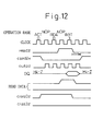
- FIG. 12 is a time chart showing the operation of the first embodiment.
- FIG. 13 is a block diagram showing a configuration according to a second embodiment of the invention.
- FIG. 10 is a diagram showing a configuration of the parts related to the output of the SDRAM according to the first embodiment of the invention. The other parts have the same configuration as shown in FIG. 1 .
- a column activation signal extension circuit 51 is interposed between the column activation signal generating circuit 33 and a output clock buffer 34 for extending the column activation signal csex by one clock cycle to produce an extended column activation signal csedlx.
- the extended column activation signal csedlx is input to the output clock buffer 34 in place of the column activation signal csex.
- the other parts have the same configuration as the corresponding parts shown in FIG. 1 .
- FIG. 11 is a diagram showing a configuration of the column activation signal extension circuit 51 .
- the input column activation signal csex is delayed by one cycle of clock clkz using a flip-flop operated at the internal clock clkz, and synthesized with the signal csex thereby to generate the extended column activation signal csedlx.
- the signal csedlx is validated by falling the same way as the signal csex, and invalidated by rising one clock cycle behind.
- the column activation signal extension circuit 51 extends the column activation signal csex by one cycle of clock clkz.
- the extension can be further lengthened, however, in order to make sure that the output DQ assumes a high impedance without fail in case of a fault.
- FIG. 13 is a diagram showing a configuration of the parts related to the output of the SDRAM according to the second embodiment of the invention. The other parts are the same as the corresponding parts shown in FIG. 1 .
- this embodiment is different from the prior art in that an output clock delay circuit 52 is added for delaying, by one cycle, the output clock outpz produced from the output clock buffer 34 .
- the output clock delay circuit 52 produces a delayed output clock doutpz delayed by one cycle from the signal outpz.
- the output circuit 36 is supplied with the signal doutpz in place of the signal outpz, and the output changes in synchronism with the signal doutpz.
- the signal doutpz is one cycle delayed behind the signal outpz, and therefore this circuit has substantially the same effect as producing one more extra pulse of the output clock.
- the high impedance data is set in the output circuit 36 by the last pulse, so that the output DQ of the output circuit assumes a high impedance.
- the first two pulses of the output clock outpz are not actually used, and therefore this delay has no adverse effect on the start of the output.
Landscapes
- Dram (AREA)
- Semiconductor Memories (AREA)
Applications Claiming Priority (2)
| Application Number | Priority Date | Filing Date | Title |
|---|---|---|---|
| JP11-121629 | 1999-04-28 | ||
| JP12162999A JP4266436B2 (ja) | 1999-04-28 | 1999-04-28 | 半導体記憶装置 |
Publications (1)
| Publication Number | Publication Date |
|---|---|
| US6269048B1 true US6269048B1 (en) | 2001-07-31 |
Family
ID=14816003
Family Applications (1)
| Application Number | Title | Priority Date | Filing Date |
|---|---|---|---|
| US09/515,508 Expired - Lifetime US6269048B1 (en) | 1999-04-28 | 2000-02-29 | Semiconductor memory device for inputting/outputting data through a common terminal and outputting data in synchronism with clock |
Country Status (2)
| Country | Link |
|---|---|
| US (1) | US6269048B1 (ja) |
| JP (1) | JP4266436B2 (ja) |
Cited By (6)
| Publication number | Priority date | Publication date | Assignee | Title |
|---|---|---|---|---|
| US6438658B1 (en) * | 2000-06-30 | 2002-08-20 | Intel Corporation | Fast invalidation scheme for caches |
| US6480439B2 (en) * | 2000-10-03 | 2002-11-12 | Mitsubishi Denki Kabushiki Kaisha | Semiconductor device |
| US6504789B2 (en) * | 1999-12-27 | 2003-01-07 | Nec Corporation | Semiconductor memory device |
| US6754134B1 (en) * | 2003-09-25 | 2004-06-22 | International Business Machines Corporation | Semiconductor storage device having multiple interrupt feature for continuous burst read and write operation |
| US20040160853A1 (en) * | 2003-02-17 | 2004-08-19 | Renesas Technology Corp. | Semiconductor memory device inputting/outputting data and parity data in burst operation |
| US10043577B2 (en) | 2016-03-08 | 2018-08-07 | Toshiba Memory Corporation | Semiconductor memory device |
Families Citing this family (3)
| Publication number | Priority date | Publication date | Assignee | Title |
|---|---|---|---|---|
| JP5226161B2 (ja) * | 2001-02-23 | 2013-07-03 | 富士通セミコンダクター株式会社 | 半導体記憶装置および情報処理システム |
| KR100638747B1 (ko) * | 2004-12-28 | 2006-10-30 | 주식회사 하이닉스반도체 | 반도체 기억 소자의 클럭 생성 장치 및 방법 |
| JP5218635B2 (ja) * | 2011-12-28 | 2013-06-26 | 富士通セミコンダクター株式会社 | 半導体記憶装置 |
Citations (4)
| Publication number | Priority date | Publication date | Assignee | Title |
|---|---|---|---|---|
| US5311483A (en) * | 1990-11-20 | 1994-05-10 | Oki Electric Industry Co., Ltd. | Synchronous type semiconductor memory |
| US5402389A (en) * | 1994-03-08 | 1995-03-28 | Motorola, Inc. | Synchronous memory having parallel output data paths |
| US5666321A (en) * | 1995-09-01 | 1997-09-09 | Micron Technology, Inc. | Synchronous DRAM memory with asynchronous column decode |
| US6005825A (en) * | 1997-12-04 | 1999-12-21 | Samsung Electronics Co., Ltd. | Synchronous semiconductor memory device having wave pipelining control structure and method for outputting data using the same |
-
1999
- 1999-04-28 JP JP12162999A patent/JP4266436B2/ja not_active Expired - Fee Related
-
2000
- 2000-02-29 US US09/515,508 patent/US6269048B1/en not_active Expired - Lifetime
Patent Citations (4)
| Publication number | Priority date | Publication date | Assignee | Title |
|---|---|---|---|---|
| US5311483A (en) * | 1990-11-20 | 1994-05-10 | Oki Electric Industry Co., Ltd. | Synchronous type semiconductor memory |
| US5402389A (en) * | 1994-03-08 | 1995-03-28 | Motorola, Inc. | Synchronous memory having parallel output data paths |
| US5666321A (en) * | 1995-09-01 | 1997-09-09 | Micron Technology, Inc. | Synchronous DRAM memory with asynchronous column decode |
| US6005825A (en) * | 1997-12-04 | 1999-12-21 | Samsung Electronics Co., Ltd. | Synchronous semiconductor memory device having wave pipelining control structure and method for outputting data using the same |
Cited By (7)
| Publication number | Priority date | Publication date | Assignee | Title |
|---|---|---|---|---|
| US6504789B2 (en) * | 1999-12-27 | 2003-01-07 | Nec Corporation | Semiconductor memory device |
| US6438658B1 (en) * | 2000-06-30 | 2002-08-20 | Intel Corporation | Fast invalidation scheme for caches |
| US6480439B2 (en) * | 2000-10-03 | 2002-11-12 | Mitsubishi Denki Kabushiki Kaisha | Semiconductor device |
| US20040160853A1 (en) * | 2003-02-17 | 2004-08-19 | Renesas Technology Corp. | Semiconductor memory device inputting/outputting data and parity data in burst operation |
| US7075851B2 (en) * | 2003-02-17 | 2006-07-11 | Renesas Technology Corp. | Semiconductor memory device inputting/outputting data and parity data in burst operation |
| US6754134B1 (en) * | 2003-09-25 | 2004-06-22 | International Business Machines Corporation | Semiconductor storage device having multiple interrupt feature for continuous burst read and write operation |
| US10043577B2 (en) | 2016-03-08 | 2018-08-07 | Toshiba Memory Corporation | Semiconductor memory device |
Also Published As
| Publication number | Publication date |
|---|---|
| JP2000311488A (ja) | 2000-11-07 |
| JP4266436B2 (ja) | 2009-05-20 |
Similar Documents
| Publication | Publication Date | Title |
|---|---|---|
| US6014340A (en) | Synchronous semiconductor memory device having internal circuitry enabled only when commands are applied in normal sequence | |
| US6466511B2 (en) | Semiconductor memory having double data rate transfer technique | |
| JP3351953B2 (ja) | モードレジスタ制御回路およびこれを有する半導体装置 | |
| US6175905B1 (en) | Method and system for bypassing pipelines in a pipelined memory command generator | |
| JP2010135065A (ja) | ダイナミック・ランダム・アクセス・メモリ・システム | |
| US20030217225A1 (en) | Semiconductor memory device having external data load signal and serial-to-parallel data prefetch method thereof | |
| JP2003249077A (ja) | 半導体記憶装置及びその制御方法 | |
| US5749086A (en) | Simplified clocked DRAM with a fast command input | |
| JP5627197B2 (ja) | 半導体記憶装置及びこれを備える情報処理システム並びにコントローラ | |
| US6557090B2 (en) | Column address path circuit and method for memory devices having a burst access mode | |
| JP2000030456A (ja) | メモリデバイス | |
| US6269048B1 (en) | Semiconductor memory device for inputting/outputting data through a common terminal and outputting data in synchronism with clock | |
| JP4079507B2 (ja) | メモリ制御システムおよびメモリ制御方法 | |
| US6026041A (en) | Semiconductor memory device | |
| US8996738B2 (en) | Data transfer operation completion detection circuit and semiconductor memory device provided therewith | |
| US7180822B2 (en) | Semiconductor memory device without decreasing performance thereof even if refresh operation or word line changing operation occur during burst operation | |
| JP2002015570A (ja) | 半導体メモリ | |
| US6192002B1 (en) | Memory device with command buffer | |
| JP2003317477A (ja) | 半導体記憶装置 | |
| JPH06282983A (ja) | メモリ内のデータをアクセスするための方法、メモリシステムおよびメモリ制御システム | |
| US7548465B2 (en) | Low current consumption semiconductor memory device | |
| US11366487B2 (en) | Resetting clock divider circuitry prior to a clock restart | |
| US7224623B2 (en) | Memory device having off-chip driver enable circuit and method for reducing delays during read operations | |
| JP3237583B2 (ja) | 同期型半導体記憶装置及びこれを用いた半導体記憶システム | |
| US20070073961A1 (en) | Memory controller |
Legal Events
| Date | Code | Title | Description |
|---|---|---|---|
| AS | Assignment |
Owner name: FUJITSU LIMITED, JAPAN Free format text: ASSIGNMENT OF ASSIGNORS INTEREST;ASSIGNORS:KANO, HIDEKI;YAMADA, SHINICHI;SAITOH, SATORU;REEL/FRAME:010594/0505 Effective date: 20000223 |
|
| STCF | Information on status: patent grant |
Free format text: PATENTED CASE |
|
| FEPP | Fee payment procedure |
Free format text: PAYOR NUMBER ASSIGNED (ORIGINAL EVENT CODE: ASPN); ENTITY STATUS OF PATENT OWNER: LARGE ENTITY |
|
| FPAY | Fee payment |
Year of fee payment: 4 |
|
| AS | Assignment |
Owner name: FUJITSU MICROELECTRONICS LIMITED, JAPAN Free format text: ASSIGNMENT OF ASSIGNORS INTEREST;ASSIGNOR:FUJITSU LIMITED;REEL/FRAME:021998/0645 Effective date: 20081104 Owner name: FUJITSU MICROELECTRONICS LIMITED,JAPAN Free format text: ASSIGNMENT OF ASSIGNORS INTEREST;ASSIGNOR:FUJITSU LIMITED;REEL/FRAME:021998/0645 Effective date: 20081104 |
|
| FPAY | Fee payment |
Year of fee payment: 8 |
|
| AS | Assignment |
Owner name: FUJITSU SEMICONDUCTOR LIMITED, JAPAN Free format text: CHANGE OF NAME;ASSIGNOR:FUJITSU MICROELECTRONICS LIMITED;REEL/FRAME:024982/0245 Effective date: 20100401 |
|
| FPAY | Fee payment |
Year of fee payment: 12 |
|
| AS | Assignment |
Owner name: SOCIONEXT INC., JAPAN Free format text: ASSIGNMENT OF ASSIGNORS INTEREST;ASSIGNOR:FUJITSU SEMICONDUCTOR LIMITED;REEL/FRAME:035508/0637 Effective date: 20150302 |