US6141304A - Optical pickup - Google Patents
Optical pickup Download PDFInfo
- Publication number
- US6141304A US6141304A US09/060,162 US6016298A US6141304A US 6141304 A US6141304 A US 6141304A US 6016298 A US6016298 A US 6016298A US 6141304 A US6141304 A US 6141304A
- Authority
- US
- United States
- Prior art keywords
- wavefront
- liquid crystal
- optical disk
- laser beam
- wavefront aberration
- Prior art date
- Legal status (The legal status is an assumption and is not a legal conclusion. Google has not performed a legal analysis and makes no representation as to the accuracy of the status listed.)
- Expired - Lifetime
Links
Images


Classifications
-
- G—PHYSICS
- G11—INFORMATION STORAGE
- G11B—INFORMATION STORAGE BASED ON RELATIVE MOVEMENT BETWEEN RECORD CARRIER AND TRANSDUCER
- G11B7/00—Recording or reproducing by optical means, e.g. recording using a thermal beam of optical radiation by modifying optical properties or the physical structure, reproducing using an optical beam at lower power by sensing optical properties; Record carriers therefor
- G11B7/12—Heads, e.g. forming of the optical beam spot or modulation of the optical beam
- G11B7/135—Means for guiding the beam from the source to the record carrier or from the record carrier to the detector
- G11B7/1392—Means for controlling the beam wavefront, e.g. for correction of aberration
- G11B7/13925—Means for controlling the beam wavefront, e.g. for correction of aberration active, e.g. controlled by electrical or mechanical means
- G11B7/13927—Means for controlling the beam wavefront, e.g. for correction of aberration active, e.g. controlled by electrical or mechanical means during transducing, e.g. to correct for variation of the spherical aberration due to disc tilt or irregularities in the cover layer thickness
-
- G—PHYSICS
- G11—INFORMATION STORAGE
- G11B—INFORMATION STORAGE BASED ON RELATIVE MOVEMENT BETWEEN RECORD CARRIER AND TRANSDUCER
- G11B7/00—Recording or reproducing by optical means, e.g. recording using a thermal beam of optical radiation by modifying optical properties or the physical structure, reproducing using an optical beam at lower power by sensing optical properties; Record carriers therefor
- G11B7/08—Disposition or mounting of heads or light sources relatively to record carriers
- G11B7/09—Disposition or mounting of heads or light sources relatively to record carriers with provision for moving the light beam or focus plane for the purpose of maintaining alignment of the light beam relative to the record carrier during transducing operation, e.g. to compensate for surface irregularities of the latter or for track following
- G11B7/095—Disposition or mounting of heads or light sources relatively to record carriers with provision for moving the light beam or focus plane for the purpose of maintaining alignment of the light beam relative to the record carrier during transducing operation, e.g. to compensate for surface irregularities of the latter or for track following specially adapted for discs, e.g. for compensation of eccentricity or wobble
- G11B7/0956—Disposition or mounting of heads or light sources relatively to record carriers with provision for moving the light beam or focus plane for the purpose of maintaining alignment of the light beam relative to the record carrier during transducing operation, e.g. to compensate for surface irregularities of the latter or for track following specially adapted for discs, e.g. for compensation of eccentricity or wobble to compensate for tilt, skew, warp or inclination of the disc, i.e. maintain the optical axis at right angles to the disc
-
- G—PHYSICS
- G11—INFORMATION STORAGE
- G11B—INFORMATION STORAGE BASED ON RELATIVE MOVEMENT BETWEEN RECORD CARRIER AND TRANSDUCER
- G11B7/00—Recording or reproducing by optical means, e.g. recording using a thermal beam of optical radiation by modifying optical properties or the physical structure, reproducing using an optical beam at lower power by sensing optical properties; Record carriers therefor
- G11B7/12—Heads, e.g. forming of the optical beam spot or modulation of the optical beam
- G11B7/135—Means for guiding the beam from the source to the record carrier or from the record carrier to the detector
- G11B7/1365—Separate or integrated refractive elements, e.g. wave plates
- G11B7/1369—Active plates, e.g. liquid crystal panels or electrostrictive elements
-
- G—PHYSICS
- G11—INFORMATION STORAGE
- G11B—INFORMATION STORAGE BASED ON RELATIVE MOVEMENT BETWEEN RECORD CARRIER AND TRANSDUCER
- G11B7/00—Recording or reproducing by optical means, e.g. recording using a thermal beam of optical radiation by modifying optical properties or the physical structure, reproducing using an optical beam at lower power by sensing optical properties; Record carriers therefor
- G11B2007/0003—Recording, reproducing or erasing systems characterised by the structure or type of the carrier
- G11B2007/0006—Recording, reproducing or erasing systems characterised by the structure or type of the carrier adapted for scanning different types of carrier, e.g. CD & DVD
Definitions
- the present invention relates to an optical pickup for reading recorded information from an optical disk, and more particularly to an optical pickup of a compatible type which can be used for two types of optical disks having different thicknesses up to their recording surfaces, such as a digital video disk (DVD) and a compact disk (CD).
- DVD digital video disk
- CD compact disk
- the DVD is an optical disk capable of large volumes of digital information, and allows digital information, such as moving pictures, computer information and the like, to be recorded on a disk having the same 12 cm diameter as the CD with a recording density approximately eight times or more as large as that of the CD.
- various devices have been made to attain such a high-density recording.
- the wavelength of a laser light source used is set at 650 nm which is shorter than 780 nm for the CD, and the numerical aperture NA of an objective lens is set at 0.6 which is larger than 0.45 for the CD, thereby attaining high-density recording of about 5 G bytes on one surface of the disk.
- the DVD since the DVD allows higher-density recording than the CD, it is necessary to make the spot diameter of a laser beam for reading pit information much smaller than that in the case of the CD.
- the spot diameter of the laser beam is proportional to the wavelength ⁇ of the laser used, and is inversely proportional to the numerical aperture NA of the objective lens.
- the spot diameter is made small by using a laser light source having a short wavelength and an objective lens having a large numerical aperture NA.
- wavefront aberration mainly coma-aberration
- the margin for a so-called tilt angle i.e., the angle at which the disk surface is tilted from a perpendicular direction to the optical axis of the objective lens of the optical pickup, becomes small.
- the DVD and the CD are optical disks of the same form, and it is desirable to allow the CD to be reproduced by a DVD player.
- the substrate of the disk of the CD is thicker than that of the DVD (e.g., 1.2 mm for one side of the CD as compared to 0.6 mm for one side of the DVD)
- wavefront aberration mainly spherical aberration
- the optical pickup which is optimally designed for the DVD is used as it is, the information of the CD cannot be read.
- tilt correction it is difficult to simultaneously effect correction with respect to the tilting of the disk (hereafter referred to as the tilt correction), so that it is necessary to provide a tilt correcting means separately.
- the optical pickup apparatus becomes large in size, and the cost becomes high.
- This apparatus is arranged such that a liquid crystal device is disposed in the optical path of the optical pickup, voltage is applied to the liquid crystal device in correspondence with the detected tilt angle to impart a phase difference to the passing bundle of rays, thereby correcting the effect of wavefront aberration ascribable to the tilt angle.
- the conventional liquid crystal device has not been optimized with respect to the wavefront aberration ascribable to the tilt angle, and has been impossible to completely eliminate the wavefront aberration. Hence, the effect of the wavefront aberration has remained, and it has been impossible to obtain favorable reproducing characteristics.
- the present invention has been devised in view of the above-described problems, and its object is to provide an optical pickup which is capable of reliably correcting the effect of the wavefront aberration ascribable to the tilt angle.
- an optical pickup including, a laser light source emitting a laser beam, an objective lens collecting the laser beam; and a wavefront-aberration correcting device provided on an optical axis of the laser beam and adapted to change a refractive index by controlling voltage.
- the wavefront-aberration correcting device has an electrode, and the electrode is divided into a configuration corresponding to a distribution of wavefront aberration ascribable to a tilt angle of an optical disk.
- the electrode provided in the wavefront-aberration correcting device is divided into a configuration corresponding to the distribution of wavefront aberration ascribable to the tilt angle of the optical disk. Accordingly, even if the optical disk is tilted during the reproduction of the optical disk, the wavefront-aberration correcting device corrects the light spot formed on the recording surface of the optical disk in such a manner as to suppress the value of wavefront aberration ascribable to the tilt of the optical disk within a predetermined range, so that reproduction can be effected satisfactorily.
- an optical pickup including, a laser light source emitting a laser beam, an objective lens collecting the laser beam, and a wavefront-aberration correcting device provided on an optical axis of the laser beam and adapted to change a refractive index by controlling voltage.
- the wavefront-aberration correcting device has a pair of electrodes, one of the electrodes is a first electrode divided into a configuration corresponding to a distribution of wavefront aberration ascribable to a tilt angle of an optical disk, and the other of the electrodes is a second electrode divided into a configuration for correcting wavefront aberration ascribable to the thickness of a substrate of said optical disk to be reproduced.
- one of a pair of electrodes of the wavefront-aberration correcting device is divided into a configuration corresponding to the distribution of wavefront aberration ascribable to the tilt angle of the optical disk, and the other one of the pair of electrodes is divided into a configuration for correcting wavefront aberration ascribable to the thickness of the substrate of the optical disk to be reproduced.
- the wavefront-aberration correcting device corrects the light spot formed on the recording surface of the optical disk in such a manner as to suppress the value of wavefront aberration ascribable to the tilt of the optical disk within a predetermined range and the value of wavefront aberration ascribable to the thickness of the substrate of the optical disk to be reproduced within a predetermined range, so that optical disks whose substrates have different thicknesses can be reproduced satisfactorily, respectively.
- an optical pickup including, a laser light source emitting a laser beam, an objective lens collecting the laser beam; and a wavefront-aberration correcting device provided on an optical axis of the laser beam and adapted to change a refractive index by controlling voltage, wherein the wavefront-aberration correcting device has an electrode, and the electrode is divided into a configuration corresponding to a distribution of wavefront aberration ascribable to a tilt angle of an optical disk and into a configuration for correcting wavefront aberration ascribable to the thickness of a substrate of said optical disk.
- one of a pair of electrodes of the wavefront-aberration correcting device is formed by being divided into a configuration corresponding to the distribution of wavefront aberration ascribable to the tilt angle of the optical disk and into a configuration for correcting wavefront aberration ascribable to the thickness of the substrate of the optical disk to be reproduced.
- the wavefront-aberration correcting device corrects the light spot formed on the recording surface of the optical disk in such a manner as to suppress the value of wavefront aberration ascribable to the tilt of the optical disk within a predetermined range and the value of wavefront aberration ascribable to the thickness of the substrate of the optical disk to be reproduced within a predetermined range, so that optical disks whose substrates have different thicknesses can be reproduced satisfactorily, respectively.
- FIG. 1 is a diagram explaining the basic principle of the optical pickup in accordance with a first embodiment of the present invention
- FIG. 2 is a cross-sectional view of an example of the structure of the liquid crystal panel in accordance with the first embodiment
- FIG. 3 is a diagram explaining liquid crystal molecules
- FIGS. 4A to 4C are diagrams explaining the change in refractive index of a liquid crystal due to the difference in applied voltage
- FIGS. 5A and 5B are diagrams illustrating the divided configurations of a transparent electrode
- FIG. 6 is a diagram illustrating the distribution of the wavefront aberration in correspondence with the lens diameter of an objective lens used in the convergence of a laser beam
- FIG. 7 is a diagram illustrating a distribution characteristic of wavefront aberration
- FIG. 8A is a diagram illustrating the wavefront aberration occurring in the case where the optical disk is tilted
- FIG. 8B is a diagram illustrating the distribution of residual wavefront aberration after correction of phase difference
- FIG. 9 is a graphic showing the simulated results of the wavefront aberration of a light spot, which is formed on the recording surface of the optical disk by the optical pickup in accordance with the first embodiment of the present invention, for each tilt angle (in the radial direction) of the disk;
- FIGS. 10A to 10F are diagrams which illustrate other examples of electrode patterns divided by transparent electrodes of the liquid crystal panel
- FIGS. 11A to 11D are diagrams explaining the liquid crystal panel in accordance with a second embodiment of the present invention, in which FIG. 11A is a cross-sectional structural diagram of the liquid crystal panel, FIG. 11B represents an orientation of the liquid crystal, FIG. 11C is a diagram illustrating the divided configurations of a transparent electrode 302c, and FIG. 11D is a diagram illustrating the divided configurations of a transparent electrode 302a;
- FIGS. 12A and 12B are cross-sectional views illustrating the states of orientation of the liquid crystal molecules in the liquid crystal panel controlled by the liquid-crystal-panel controlling circuit of the optical pickup in accordance with the second embodiment;
- FIGS. 13A and 13B are diagrams explaining the liquid crystal panel in accordance with a third embodiment of the present invention
- FIG. 13A is a cross-sectional structural diagram of the liquid crystal panel
- FIG. 13B is a diagram illustrating the divided configurations of a transparent electrode
- FIGS. 14A and 14B are diagrams illustrating the state of application of voltage to areas of the transparent electrode of the liquid crystal panel for which the voltage is controlled by the liquid-crystal-panel controlling circuit in the optical pickup in accordance with the third embodiment.
- FIG. 15 is a graphic showing the simulated results of the wavefront aberration of a light spot, which is formed on the recording surface of the DVD by the optical pickup in accordance with the third embodiment of the present invention, for each tilt angle (in the radial direction) of the disk.
- FIG. 1 is a diagram explaining the basic principle of the optical pickup in accordance with a first embodiment of the present invention.
- reference numeral 1 denotes a laser light source; 2, a polarization beam splitter; 3, a liquid crystal panel serving as a liquid crystal device; 4, a quarter-wave plate; 5, an objective lens; 6, an optical disk; 7, a condenser lens; 8, a light-receiving device; 9, a tilt sensor for detecting the tilt angle; and 10, a liquid-crystal-panel controlling circuit.
- the laser beam emitted from the laser light source 1 passes through the polarization beam splitter 2, passes through the liquid crystal panel 3 and the quarter-wave plate 4, is then collected by the objective lens 5, and forms a focal point on an information recording surface of the optical disk 6.
- the reflected light of the laser beam reflected by the information recording surface of the optical disk 6 passes again through the objective lens 5 and the liquid crystal panel 3, then has its optical path changed by the polarization beam splitter 2, and forms an image on the light receiving device 8 via the condenser lens 7.
- the aforementioned quarter-wave plate 4 is disposed in such a manner as to intersect at an angle of 45° with respect to the plane of polarization P of the laser beam converted to linearly polarized waves by the polarization beam splitter 2.
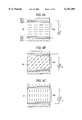
- FIG. 2 shows a cross-sectional view of an example of the structure of the liquid crystal panel in accordance with the first embodiment.
- numerals 301a and 301b denote transparent glass substrates, and transparent electrodes 302a and 302b formed of indium-tin oxide (ITO) or the like are deposited on inner surfaces of these glass substrates.
- An electrode pattern having a plurality of divided areas is formed on the transparent electrode 302a, and the divided areas are formed in such a manner that voltage can be applied thereto independently, respectively.
- Oriented films 303a and 303b for imparting predetermined molecular orientation to a liquid crystal are respectively formed on inner surfaces of these transparent electrodes 302a and 302b, and a birefringent liquid crystal 304 such as a nematic liquid crystal is sealed in between the oriented films 303a and 303b.
- the liquid crystal panel 3 is formed with a range wider than a maximum region of an incident laser beam.
- the liquid crystal 304 one is used which has different refractive indices depending on the direction of the optical axis of a liquid crystal molecule M and a direction perpendicular thereto, as shown in FIG. 3, i.e., a liquid crystal which exhibits a birefringent effect.
- the orientation of the liquid crystal molecule M can be changed freely from the horizontal direction to the perpendicular direction, as shown in FIGS. 4A to 4C.
- the liquid-crystal-panel controlling circuit 10 calculates the voltage to be applied to each divided area of the transparent electrode 302a in correspondence with the result of detection by the tilt sensor 9, and outputs the same to the liquid crystal panel 3.
- the wavefront aberration at the pupil plane of the objective lens is assumed to be W(r, ⁇ ) where (r, ⁇ ) are the polar coordinates of the pupil plane.
- the wavefront aberration (mainly coma-aberration) occurs, and it becomes impossible to diaphragm the laser beam by means of the objective lens.
- principal components of the wavefront aberration WTLT(r, ⁇ ) ascribable to the tilt angle can be expressed by the following formula (1):
- w 31 and w 11 are constants which are given by the tilt angle of the optical disk, the thickness of the substrate, the refractive index of the substrate, and NA, and w 31 represents coma-aberration, while w 11 represents aberration due to the movement of an image point.
- the result of calculation of a wavefront aberration distribution in the pupil plane by using this formula corresponds to the wavefront aberration distribution shown in FIG. 6 which will be referred to later.
- Wrms Wrms
- the liquid crystal panel 3 is divided in correspondence with the distribution of the wavefront aberration ascribable to the tilt angle of the optical disk, which is shown in FIG. 6, and if the voltage to be applied to each divided area is controlled in such a manner as to impart wavefront aberration of polarity opposite to the wavefront aberration ascribable to the tilt angle.
- the liquid crystal panel 3 is divided into a checkered form, that is, the number of divisions is increased too much, it is necessary to apply a control voltage to each divided area.
- the transparent electrodes of the liquid crystal panel 3 must be prepared in correspondence with the respective divided areas, and it is difficult to prepare the transparent electrodes and the wiring of leads.
- the above-described preparation is readily possible by forming the divided configuration of the liquid crystal panel 3 (the configuration of the divided transparent electrodes) into a divided configuration corresponding to the distribution of the wavefront aberration ascribable to the tilt angle as shown in FIGS. 5A and 5B referred to earlier, and the wavefront aberration ascribable to the tilt angle of the optical disk is corrected efficiently.
- FIG. 6 shows the distribution of the wavefront aberration occurring in the pupil plane of the objective lens at this time.
- FIG. 6 is a diagram in which the distribution of the wavefront aberration at a best image point of the light spot S' in a case where the recording surface of the disk is tilted +1 is shown within the range of the maximum region 11 of the incident light beam, and is shown by boundary lines of regions A to K which center on the region A whose value of wavefront aberration has a range of -25 nm to +25 nm and which are respectively located above or below the region A at 50 nm intervals.
- Line X2--X2 in FIG. 6 is an axis corresponding to the direction in which the optical disk is tilted
- FIG. 7 is a diagram in which this distribution of wavefront aberration is shown by the distribution characteristic on the axis x2--X2.
- the distribution itself of the wavefront aberration exhibits a fixed distribution irrespective of the tilt angle, and the amount of wavefront aberration varies depending on the magnitude of the tilt angle. That is, as for the peak value of the curve shown in FIG. 7, the higher the tilt angle, the higher the peak, and the smaller the tilt angle, the lower the peak.
- the configurations of the electrode patterns shown in FIGS. 5A and 5B are set on the basis of the wavefront aberration distribution (shown in FIG. 6) in the case where the recording surface of the optical disk is tilted +1°.
- FIG. 5A an electrode pattern is formed which has a configuration in which the values of wavefront aberration are divided into three parts by areas 12 to 14 obtained by dividing the values of wavefront aberration into three ranges, for instance.
- FIG. 8A is a diagram illustrating the wavefront aberration occurring in the case where the optical disk is tilted
- FIG. 8B is a diagram illustrating the distribution of residual wavefront aberration after correction of the wavefront aberration.
- the liquid-crystal-panel controlling circuit 10 provides control so as to apply a predetermined control voltage to the electrode corresponding to the area 17 in FIG. 5B so that the phase difference of the light beam transmitted therethrough becomes 0, and to apply a control voltage to the other electrodes corresponding to the areas 15, 16, 18, and 19 to correct the amount of phase difference shown by the dotted line in FIG. 8A.
- the following voltages are applied from the liquid-crystal-panel controlling circuit 10 to the respective areas: a voltage for imparting a phase difference of -75 nm to the area 15, a voltage for imparting a phase difference of +75 nm to the area 16, a voltage for imparting a phase difference of -75 nm to the area 18, and a voltage for imparting a phase difference of +75 nm to the area 19.
- the liquid crystal molecules only have to be oriented in advance such that the phase difference of the light beam passing through the area 17 becomes 0.
- only one kind of voltage may be used as the voltage for controlling the amount of phase difference for the liquid crystal panel as a whole, if its polarity is not taken into consideration.
- control is provided in such a manner that the same voltage as that of the areas 16 and 18 of the five-divided pattern in FIG. 5B is applied to the areas 12 and 13, respectively, of the three-divided electrode in FIG. 5A, and a phase difference is not imparted to the transmitting light flux in the area 14.
- the liquid-crystal-panel controlling circuit 10 can be controlled so as to apply such a predetermined control voltage to the electrode corresponding to the area 14 that the phase difference of the light beam transmitted therethrough becomes 0, and to apply a control voltage equal in magnitude but opposite in polarity to the electrodes corresponding to the other areas 12 and 13.
- a control voltage equal in magnitude but opposite in polarity to the electrodes corresponding to the other areas 12 and 13.
- only two kinds of voltage may be used as the voltage for controlling the amount of phase difference for the liquid crystal panel as a whole if its polarity is not taken into consideration.
- the liquid crystal molecules only have to be oriented in advance so that the phase difference of the light beam passing through the area 14 becomes 0.
- only one kind of voltage may be used as the voltage for controlling the amount of phase difference for the liquid crystal panel as a whole if its polarity is not taken into consideration.
- the divided configuration of the transparent electrode 302a has only to be set on the basis of the distribution of the wavefront aberration ascribable to the tilt angle of the optical disk at the pupil plane of the objective lens.
- FIGS. 10A to 10F Patterns of other divided configurations of the transparent electrode 302a are shown in FIGS. 10A to 10F.
- the divided configurations shown in FIGS. 10A to 10F also can be reduced within a range which the effect of wavefront aberration ascribable to the tilt angle does not present a problem in reproduction.
- the optical pickup in accordance with the second embodiment of the present invention is arranged by using a liquid crystal panel 20 instead of the liquid crystal panel 3 in the optical pickup shown in FIG. 1.
- the transparent electrode 302c is an electrode for correcting the spherical aberration occurring due to the difference in thickness of the substrates of two different kinds of optical disks. As shown in: FIG. 11C, in the maximum region 11 of the incident laser beam, the transparent electrode 302c is divided into configurations corresponding to two areas shown by a circular aperture area 22 (the hatched portion) restricted to a central portion and by an area 23 (the hatched portion) adjacent to an outer peripheral portion of the area 22.
- the liquid crystal 304 used in the liquid crystal panel 20 is formed between the transparent electrodes 302a and 302c in a state of being twist-oriented at a predetermined angle ⁇ .
- the plane of polarization of this reflected beam returned to the linearly polarized light is one which is rotated 90° from the original plane of linear polarization, and this reflected beam is a polarized wave oriented perpendicular to the plane of polarization of the polarization beam splitter 2.
- This reflected beam constituted by linearly polarized light rotated 90° passes as it is through the liquid crystal panel 20 acting as a transparent plate, and reaches the polarization beam splitter 2.
- the reflected beam is reflected in the horizontal direction by the plane of polarization of the polarization beam splitter 2, and is received by the light receiving device 8 via the condenser lens 7.
- the overall area of the liquid crystal panel 20 acts as a mere transparent plate during the reading of the information recorded on the DVD, all the reflected light from the disk can be transmitted to the light receiving device 8. For this reason, when the information recorded on the DVD is read, the entire area of the objective lens 5 is used.
- the liquid-crystal-panel controlling circuit 10 effects the tilt correction of the DVD by controlling the transparent electrode 302a in the same way as in the first embodiment, even if the DVD is tilted, the light spot formed on the recording surface of the optical disk can be suppressed within a predetermined range in terms of the value of wavefront aberration ascribable to the tilt of the DVD. At the same time, it is possible to obtain sufficient reflected light intensity sufficient for reading the recorded information.
- FIGS. 12A and 12B are cross-sectional views in which the states of orientation of the liquid crystal molecules M in the liquid crystal 304 corresponding to the respective areas are shown along the axis X2--X2 in a case where the liquid-crystal-panel controlling circuit 10 of the optical pickup in accordance with the second embodiment controls the voltage for each area of the divided electrode of the liquid crystal panel 20.
- FIG. 12A is a diagram illustrating a case in which the optical pickup reads the recorded information of the DVD
- FIG. 12B is a diagram illustrating a case in which the optical pickup reads the recorded information of the CD.
- the liquid-crystal-panel controlling circuit 10 controls the voltage to be applied to each area of the transparent electrode 302a after temporarily orienting the liquid crystal molecules M in a perpendicular direction (oriented in the vertical direction in the drawing), so that the orientation of the liquid crystal molecules M is controlled for each area in correspondence with the tilt of the DVD.
- the liquid-crystal-panel controlling circuit 10 perpendicularly orients the liquid crystal molecules M corresponding to the area 22, and twist-orients the liquid crystal molecules M corresponding to the area 23.
- a CD selection signal is imparted to the liquid-crystal-panel controlling circuit 10.
- the liquid-crystal-panel controlling circuit 10 applies voltage to the electrode corresponding to the area 22 provided in the transparent electrode 302c of the liquid crystal panel 20, and effects control such that the liquid crystal molecules M of the liquid crystal 304 corresponding to the area 22 assume a substantially perpendicularly oriented state by its electric field. Then, the portion of the liquid crystal panel at the area 22 becomes a mere transparent plate due to the action similar to the one described before.
- the liquid-crystal-panel controlling circuit 10 effects control such that the voltage applied to the area 23 becomes 0 (ground potential), so that no electric field acts on the liquid crystal molecules M of the liquid crystal 304 corresponding to the area 23.
- the liquid crystal molecules M of the liquid crystal 304 corresponding to the area 23 remain in the twist-oriented state.
- the reflected light passing through the area 23 has its plane of polarization rotated along the twisted liquid crystal molecules M, and is made incident upon the quarter-wave plate 4.
- the laser beam incident upon the quarter-wave plate 4 since its plane of polarization is oriented in a substantially similar direction as that of the crystal axis of the quarter-wave plate 4, that laser beam passes through the quarter-wave plate 4 without being substantially affected by the effect of the quarter-wave plate 4, and after it is reflected by the information recording surface of the CD, that laser beam is made incident upon the quarter-wave plate 4.
- the reflected light incident upon the quarter-wave plate 4 passes again through the quarter-wave plate 4 as it is in the form of the linearly polarized light without being substantially affected by the effect of the quarter-wave plate 4, and is made incident upon the liquid crystal panel 20.
- This reflected light constituted by the linearly polarized light when passing through the liquid crystal panel 20, has its plane of polarization rotated along the twist of the liquid crystal molecules M.
- this reflected light emerges from the liquid crystal panel 20, its direction of polarization becomes substantially similar to that of the original plane of polarization of the laser beam.
- the laser beam reflected by the CD after passing through the area 23 of the liquid crystal panel 20 is transmitted as it is through the polarization beam splitter 2, that laser beam is not made incident upon the light receiving device 8.
- a DVD selection signal is imparted to the liquid-crystal-panel controlling circuit 10.
- the liquid-crystal-panel controlling circuit 10 applies a predetermined voltage uniformly to the respective electrodes corresponding to the areas 24 to 29 provided in the transparent electrode 302d of the liquid crystal panel 21, and thereby effecting control such that all the liquid crystal molecules of the liquid crystal 304 are set in a substantially perpendicularly oriented state by the electric field. Consequently, the overall area of the liquid crystal panel 21 acts as a mere transparent plate, and the polarizing action due to twist practically disappears.
- This reflected beam constituted by linearly polarized light rotated 90° passes as it is through the liquid crystal panel 21 acting as a transparent plate, and reaches the polarization beam splitter 2.
- the reflected beam is reflected in the horizontal direction by the plane of polarization of the polarization beam splitter 2, and is received by the light receiving device 8 via the condenser lens 7.
- the liquid-crystal-panel controlling circuit 10 effects control by changing for each of the areas 24 to 29 the predetermined voltage applied uniformly to each electrode.
- the liquid crystal molecules M of the liquid crystal 304 corresponding to the areas 25, 28, and 29 remain in the twist-oriented state.
- the reflected light passing through the areas 25, 28, and 29 has its plane of polarization rotated along the twisted liquid crystal molecules M, and is made incident upon the quarter-wave plate 4.
- FIG. 15 is a graphic representation of the results of simulation of the wavefront aberration of a light spot, which is formed on the recording surface of the DVD by the optical pickup using the liquid crystal panel 21 arranged as described above, for each tilt angle (in the radial direction) of the disk.
- the result of simulation of a case where the transparent electrode 302d is formed in a six-divided pattern and the circular region formed by areas 24, 26, and 27 is set to circular ranges respectively having diameters of 2.2 mm and 2.5 mm is shown in comparison with the result of simulation of the wavefront aberration in a case where the transparent electrode 302d is not divided (no correction).
- one of a pair of electrodes of the wavefront-aberration correcting device is divided into a configuration corresponding to the distribution of wavefront aberration ascribable to the tilt angle of the optical disk, and the other one of the pair of electrodes is divided into a configuration for correcting wavefront aberration ascribable to the thickness of the substrate of the optical disk to be reproduced.
- the wavefront-aberration correcting device corrects the light spot formed on the recording surface of the optical disk in such a manner as to suppress the value of wavefront aberration ascribable to the tilt of the optical disk within a predetermined range and the value of wavefront aberration ascribable to the thickness of the substrate of the optical disk to be reproduced within a predetermined range, so that optical disks whose substrates have different thicknesses can be reproduced satisfactorily, respectively.
Applications Claiming Priority (2)
| Application Number | Priority Date | Filing Date | Title |
|---|---|---|---|
| JP11446697A JP3538520B2 (ja) | 1997-04-16 | 1997-04-16 | 収差補正用液晶パネル、光ピックアップ及び情報再生装置 |
| JP9-114466 | 1997-04-16 |
Publications (1)
| Publication Number | Publication Date |
|---|---|
| US6141304A true US6141304A (en) | 2000-10-31 |
Family
ID=14638448
Family Applications (1)
| Application Number | Title | Priority Date | Filing Date |
|---|---|---|---|
| US09/060,162 Expired - Lifetime US6141304A (en) | 1997-04-16 | 1998-04-15 | Optical pickup |
Country Status (2)
| Country | Link |
|---|---|
| US (1) | US6141304A (ja) |
| JP (1) | JP3538520B2 (ja) |
Cited By (20)
| Publication number | Priority date | Publication date | Assignee | Title |
|---|---|---|---|---|
| US20020001273A1 (en) * | 2000-04-14 | 2002-01-03 | Mitsuhiro Togashi | Optical pickup |
| US20020060958A1 (en) * | 2000-11-21 | 2002-05-23 | Hideo Ando | Optical information processing system using optical aberrations and information medium having recording layer protected by transparent layer having thickness irregularity |
| EP1213711A2 (en) * | 2000-12-01 | 2002-06-12 | Pioneer Corporation | Device and method for controlling tilt servo |
| EP1213712A2 (en) * | 2000-12-01 | 2002-06-12 | Pioneer Corporation | Device and method for controlling tilt servo |
| US6449236B2 (en) * | 1999-12-24 | 2002-09-10 | Koninklijke Philips Electronics N. V. | Optical wavefront modifier |
| US6480454B1 (en) * | 1998-12-15 | 2002-11-12 | Matsushita Electric Industrial Co., Ltd. | Optical element, optical head using the optical element, and optical recording and reproducing apparatus using the optical element |
| US6487160B1 (en) * | 1999-03-18 | 2002-11-26 | Pioneer Corporation | Optical pickup, information recording apparatus and information reproducing apparatus |
| US6532202B1 (en) * | 1999-07-07 | 2003-03-11 | Matsushita Electric Industrial Co., Ltd. | Optical element, optical head and optical recording reproducing apparatus |
| US6552984B1 (en) * | 1999-04-13 | 2003-04-22 | Pioneer Corporation | Liquid crystal tilt servo apparatus |
| WO2004042715A1 (ja) | 2002-11-08 | 2004-05-21 | Citizen Watch Co., Ltd. | 液晶光学素子及び光学装置 |
| US6804186B2 (en) | 2000-05-24 | 2004-10-12 | Matsushita Electric Industrial Co., Ltd. | Optical pickup of tilt control type |
| EP1482491A1 (en) * | 2002-03-04 | 2004-12-01 | Matsushita Electric Industrial Co., Ltd. | Optical head and optical recording/reproducing device using it, and aberration correction method |
| EP1524655A2 (en) * | 2003-10-16 | 2005-04-20 | Pioneer Corporation | Optical pickup device and optical recording medium reproducing device |
| US20050088949A1 (en) * | 2001-06-29 | 2005-04-28 | Masahiko Tsukuda | Exposure apparatus of an optical disk master, method of exposing an optical disk master and pinhole mechanism |
| US20060012846A1 (en) * | 2004-07-16 | 2006-01-19 | Sankyo Seiki Mfg. Co., Ltd. | Aberration compensating device and optical head device |
| NL1019266C2 (nl) * | 2000-11-02 | 2006-08-08 | Sharp Kk | Optisch element. |
| US20070165500A1 (en) * | 2004-12-16 | 2007-07-19 | Sony Corporation | Optical pickup, optical disc drive employing it, and its control method |
| US20080232207A1 (en) * | 2003-10-13 | 2008-09-25 | Teunis Willem Tukker | Method and Device For Compensating Tilt of an Optical Data Carrier |
| US20100061216A1 (en) * | 2007-02-28 | 2010-03-11 | Ryuichi Katayama | Optical head unit and optcal information recording/reproducing apparatus |
| US20220264039A1 (en) * | 2015-11-05 | 2022-08-18 | Sony Semiconductor Solutions Corporation | Solid-state imaging device and electronic apparatus |
Families Citing this family (8)
| Publication number | Priority date | Publication date | Assignee | Title |
|---|---|---|---|---|
| JP4695739B2 (ja) * | 1998-12-15 | 2011-06-08 | パナソニック株式会社 | 光学素子ならびにこれを用いた光ヘッドおよび光記録再生装置 |
| JP2002304762A (ja) | 2001-04-10 | 2002-10-18 | Nec Corp | 光ヘッド装置および光学式情報記録再生装置 |
| JP4300138B2 (ja) | 2004-03-09 | 2009-07-22 | パイオニア株式会社 | 収差補正装置、並びに光ピックアップの制御装置、制御方法及び制御プログラム |
| US8018814B2 (en) | 2004-04-28 | 2011-09-13 | Pioneer Corporation | Aberration correction device, aberration correction method and optical pickup |
| JP4399324B2 (ja) | 2004-07-09 | 2010-01-13 | パイオニア株式会社 | 収差補正装置、並びに光ピックアップの制御装置、制御方法及び制御プログラム |
| JP4215011B2 (ja) | 2004-09-27 | 2009-01-28 | ソニー株式会社 | 光ピックアップ及びこれを用いた光ディスク装置 |
| JP2007017934A (ja) | 2005-06-07 | 2007-01-25 | Konica Minolta Holdings Inc | 光学素子および光ピックアップ |
| JP2007080432A (ja) * | 2005-09-15 | 2007-03-29 | Sony Corp | 光ピックアップ及びこれを用いた光ディスク装置 |
Citations (3)
| Publication number | Priority date | Publication date | Assignee | Title |
|---|---|---|---|---|
| JPH1056731A (ja) * | 1996-04-30 | 1998-02-24 | Yazaki Corp | 直流モータロック検出回路、直流モータ制御回路及び窓ガラス開閉制御装置 |
| US5859818A (en) * | 1996-09-03 | 1999-01-12 | Pioneer Electronic Corporation | Tilt servo apparatus for use in optical disc reproducing apparatus |
| US5914923A (en) * | 1996-12-09 | 1999-06-22 | Pioneer Electronic Corporation | Tilt servo system |
-
1997
- 1997-04-16 JP JP11446697A patent/JP3538520B2/ja not_active Expired - Fee Related
-
1998
- 1998-04-15 US US09/060,162 patent/US6141304A/en not_active Expired - Lifetime
Patent Citations (3)
| Publication number | Priority date | Publication date | Assignee | Title |
|---|---|---|---|---|
| JPH1056731A (ja) * | 1996-04-30 | 1998-02-24 | Yazaki Corp | 直流モータロック検出回路、直流モータ制御回路及び窓ガラス開閉制御装置 |
| US5859818A (en) * | 1996-09-03 | 1999-01-12 | Pioneer Electronic Corporation | Tilt servo apparatus for use in optical disc reproducing apparatus |
| US5914923A (en) * | 1996-12-09 | 1999-06-22 | Pioneer Electronic Corporation | Tilt servo system |
Cited By (46)
| Publication number | Priority date | Publication date | Assignee | Title |
|---|---|---|---|---|
| US6480454B1 (en) * | 1998-12-15 | 2002-11-12 | Matsushita Electric Industrial Co., Ltd. | Optical element, optical head using the optical element, and optical recording and reproducing apparatus using the optical element |
| US6487160B1 (en) * | 1999-03-18 | 2002-11-26 | Pioneer Corporation | Optical pickup, information recording apparatus and information reproducing apparatus |
| US6552984B1 (en) * | 1999-04-13 | 2003-04-22 | Pioneer Corporation | Liquid crystal tilt servo apparatus |
| US6532202B1 (en) * | 1999-07-07 | 2003-03-11 | Matsushita Electric Industrial Co., Ltd. | Optical element, optical head and optical recording reproducing apparatus |
| US6449236B2 (en) * | 1999-12-24 | 2002-09-10 | Koninklijke Philips Electronics N. V. | Optical wavefront modifier |
| JP2003518638A (ja) * | 1999-12-24 | 2003-06-10 | コーニンクレッカ フィリップス エレクトロニクス エヌ ヴィ | 光波面変更器 |
| US20020001273A1 (en) * | 2000-04-14 | 2002-01-03 | Mitsuhiro Togashi | Optical pickup |
| US6914865B2 (en) * | 2000-04-14 | 2005-07-05 | Samsung Electro-Mechanics Co., Ltd. | Device for correcting tilt aberration in an optical pickup and method therefor |
| US6804186B2 (en) | 2000-05-24 | 2004-10-12 | Matsushita Electric Industrial Co., Ltd. | Optical pickup of tilt control type |
| NL1019266C2 (nl) * | 2000-11-02 | 2006-08-08 | Sharp Kk | Optisch element. |
| US20020060958A1 (en) * | 2000-11-21 | 2002-05-23 | Hideo Ando | Optical information processing system using optical aberrations and information medium having recording layer protected by transparent layer having thickness irregularity |
| US7142484B2 (en) * | 2000-11-24 | 2006-11-28 | Kabushiki Kaisha Toshiba | Optical information processing system using optical aberrations and information medium having recording layer protected by transparent layer having thickness irregularity |
| US7224645B2 (en) | 2000-11-24 | 2007-05-29 | Kabushiki Kaisha Toshiba | Optical information processing system using optical aberrations and information medium having recording layer protected by transparent layer having thickness irregularity |
| US20050002285A1 (en) * | 2000-11-24 | 2005-01-06 | Hideo Ando | Optical information processing system using optical aberrations and information medium having recording layer protected by transparent layer having thickness irregularity |
| US6925039B2 (en) * | 2000-12-01 | 2005-08-02 | Pioneer Corporation | Device and method for controlling tilt servo |
| US7042818B2 (en) | 2000-12-01 | 2006-05-09 | Pioneer Corporation | Device and method for controlling tilt servo |
| EP1213712A3 (en) * | 2000-12-01 | 2004-09-08 | Pioneer Corporation | Device and method for controlling tilt servo |
| EP1213711A2 (en) * | 2000-12-01 | 2002-06-12 | Pioneer Corporation | Device and method for controlling tilt servo |
| US7154831B2 (en) | 2000-12-01 | 2006-12-26 | Pioneer Corporation | Device and method for controlling tilt servo |
| EP1213712A2 (en) * | 2000-12-01 | 2002-06-12 | Pioneer Corporation | Device and method for controlling tilt servo |
| US20020071364A1 (en) * | 2000-12-01 | 2002-06-13 | Pioneer Corporation | Device and method for controlling tilt servo |
| US6975574B2 (en) | 2000-12-01 | 2005-12-13 | Pioneer Corporation | Device and method for controlling tilt servo |
| EP1213711A3 (en) * | 2000-12-01 | 2004-04-07 | Pioneer Corporation | Device and method for controlling tilt servo |
| US20050270924A1 (en) * | 2000-12-01 | 2005-12-08 | Pioneer Corporation | Device and method for controlling tilt servo |
| US20050243673A1 (en) * | 2000-12-01 | 2005-11-03 | Pioneer Corporation | Device and method for controlling tilt servo |
| US20050088949A1 (en) * | 2001-06-29 | 2005-04-28 | Masahiko Tsukuda | Exposure apparatus of an optical disk master, method of exposing an optical disk master and pinhole mechanism |
| US20050078574A1 (en) * | 2002-03-04 | 2005-04-14 | Matsushita Electric Industrial Co., Ltd. | Optical head and optical recording/reproducing device using it and aberration correction method |
| EP1482491A1 (en) * | 2002-03-04 | 2004-12-01 | Matsushita Electric Industrial Co., Ltd. | Optical head and optical recording/reproducing device using it, and aberration correction method |
| EP1482491A4 (en) * | 2002-03-04 | 2008-02-20 | Matsushita Electric Ind Co Ltd | OPTICAL HEAD AND OPTICAL RECORDING / REPRODUCING DEVICE USING SUCH HEAD, AND ABERRATION CORRECTION METHOD |
| US7164638B2 (en) * | 2002-03-04 | 2007-01-16 | Matsushita Electric Industrial Co., Ltd. | Optical head and optical recording/reproducing device using it and aberration correction method |
| EP1560209A1 (en) * | 2002-11-08 | 2005-08-03 | Citizen Watch Co. Ltd. | Liquid crystal optical element and optical device |
| WO2004042715A1 (ja) | 2002-11-08 | 2004-05-21 | Citizen Watch Co., Ltd. | 液晶光学素子及び光学装置 |
| US20050174504A1 (en) * | 2002-11-08 | 2005-08-11 | Nobuyuki Hashimoto | Liquid crystal optical element and optical device |
| EP1560209A4 (en) * | 2002-11-08 | 2008-09-17 | Citizen Holdings Co Ltd | LIQUID CRYSTAL OPTICAL ELEMENT AND OPTICAL DEVICE |
| US7209426B2 (en) * | 2002-11-08 | 2007-04-24 | Citizen Watch Co., Ltd. | Liquid crystal optical element and optical device |
| US20080232207A1 (en) * | 2003-10-13 | 2008-09-25 | Teunis Willem Tukker | Method and Device For Compensating Tilt of an Optical Data Carrier |
| EP1524655A3 (en) * | 2003-10-16 | 2006-05-17 | Pioneer Corporation | Optical pickup device and optical recording medium reproducing device |
| EP1524655A2 (en) * | 2003-10-16 | 2005-04-20 | Pioneer Corporation | Optical pickup device and optical recording medium reproducing device |
| US20050083824A1 (en) * | 2003-10-16 | 2005-04-21 | Pioneer Corporation | Optical pickup device and optical recording medium reproducing device |
| US7428193B2 (en) | 2003-10-16 | 2008-09-23 | Pioneer Corporation | Optical pickup device and optical recording medium reproducing device |
| US20060012846A1 (en) * | 2004-07-16 | 2006-01-19 | Sankyo Seiki Mfg. Co., Ltd. | Aberration compensating device and optical head device |
| US20070165500A1 (en) * | 2004-12-16 | 2007-07-19 | Sony Corporation | Optical pickup, optical disc drive employing it, and its control method |
| US7796477B2 (en) * | 2004-12-16 | 2010-09-14 | Sony Corporation | Optical pick-up device having object lenses for correcting comatic aberration |
| US20100061216A1 (en) * | 2007-02-28 | 2010-03-11 | Ryuichi Katayama | Optical head unit and optcal information recording/reproducing apparatus |
| US20220264039A1 (en) * | 2015-11-05 | 2022-08-18 | Sony Semiconductor Solutions Corporation | Solid-state imaging device and electronic apparatus |
| US11838662B2 (en) * | 2015-11-05 | 2023-12-05 | Sony Semiconductor Solutions Corporation | Solid-state imaging device and electronic apparatus |
Also Published As
| Publication number | Publication date |
|---|---|
| JP3538520B2 (ja) | 2004-06-14 |
| JPH10289465A (ja) | 1998-10-27 |
Similar Documents
| Publication | Publication Date | Title |
|---|---|---|
| US6141304A (en) | Optical pickup | |
| JP3795998B2 (ja) | 波面収差補正ユニット、波面収差補正装置及び光ピックアップ | |
| JP3443226B2 (ja) | 光ピックアップ | |
| JP3476989B2 (ja) | 光ピックアップ | |
| US5513158A (en) | Optical disk pickup device with focusing correction by electrostriction | |
| US7463569B2 (en) | Optical disk apparatus with a wavelength plate having a two-dimensional array of birefringent regions | |
| JPH10269611A (ja) | 光ピックアップ及びそれを用いた多層ディスク再生装置 | |
| US6532202B1 (en) | Optical element, optical head and optical recording reproducing apparatus | |
| US20010033541A1 (en) | Aberration compensating apparatus and method | |
| EP1158335B1 (en) | Aberration correcting unit, optical pickup apparatus, and recording/reproducing apparatus | |
| JP4170712B2 (ja) | 球面収差補正装置 | |
| US7209426B2 (en) | Liquid crystal optical element and optical device | |
| JP3271890B2 (ja) | 光ピックアップ | |
| EP1524655A2 (en) | Optical pickup device and optical recording medium reproducing device | |
| US6992966B2 (en) | Optical pickup device | |
| JPH1083560A (ja) | 光ヘッド装置 | |
| US20010055262A1 (en) | Optical pickup and optical information recording/reproducing device | |
| KR20010107579A (ko) | 틸트 제어 방식 광 픽업 장치 | |
| JP4133139B2 (ja) | 光ピックアップ | |
| US6584057B1 (en) | Optical pickup system | |
| JPH09161306A (ja) | 光ディスク装置 | |
| JPH1074336A (ja) | 光ピックアップ | |
| JPH1091969A (ja) | 光ヘッド装置 | |
| JP2003173564A (ja) | 光ヘッド装置 | |
| JP2005085409A (ja) | 光ピックアップ装置 |
Legal Events
| Date | Code | Title | Description |
|---|---|---|---|
| AS | Assignment |
Owner name: PIONEER ELECTRONIC CORPORATION, JAPAN Free format text: ASSIGNMENT OF ASSIGNORS INTEREST;ASSIGNOR:OGASAWARA, MASAKAZU;REEL/FRAME:009336/0891 Effective date: 19980428 |
|
| STCF | Information on status: patent grant |
Free format text: PATENTED CASE |
|
| FPAY | Fee payment |
Year of fee payment: 4 |
|
| FEPP | Fee payment procedure |
Free format text: PAYOR NUMBER ASSIGNED (ORIGINAL EVENT CODE: ASPN); ENTITY STATUS OF PATENT OWNER: LARGE ENTITY |
|
| FPAY | Fee payment |
Year of fee payment: 8 |
|
| FPAY | Fee payment |
Year of fee payment: 12 |