US6072551A - Backlight apparatus for illuminating a display with controlled light output characteristics - Google Patents
Backlight apparatus for illuminating a display with controlled light output characteristics Download PDFInfo
- Publication number
- US6072551A US6072551A US08/782,962 US78296297A US6072551A US 6072551 A US6072551 A US 6072551A US 78296297 A US78296297 A US 78296297A US 6072551 A US6072551 A US 6072551A
- Authority
- US
- United States
- Prior art keywords
- light
- top surface
- input end
- light input
- backlight apparatus
- Prior art date
- Legal status (The legal status is an assumption and is not a legal conclusion. Google has not performed a legal analysis and makes no representation as to the accuracy of the status listed.)
- Expired - Lifetime
Links
Images


Classifications
-
- G—PHYSICS
- G02—OPTICS
- G02B—OPTICAL ELEMENTS, SYSTEMS OR APPARATUS
- G02B6/00—Light guides; Structural details of arrangements comprising light guides and other optical elements, e.g. couplings
- G02B6/0001—Light guides; Structural details of arrangements comprising light guides and other optical elements, e.g. couplings specially adapted for lighting devices or systems
- G02B6/0011—Light guides; Structural details of arrangements comprising light guides and other optical elements, e.g. couplings specially adapted for lighting devices or systems the light guides being planar or of plate-like form
- G02B6/0033—Means for improving the coupling-out of light from the light guide
- G02B6/0035—Means for improving the coupling-out of light from the light guide provided on the surface of the light guide or in the bulk of it
- G02B6/0038—Linear indentations or grooves, e.g. arc-shaped grooves or meandering grooves, extending over the full length or width of the light guide
-
- G—PHYSICS
- G02—OPTICS
- G02B—OPTICAL ELEMENTS, SYSTEMS OR APPARATUS
- G02B6/00—Light guides; Structural details of arrangements comprising light guides and other optical elements, e.g. couplings
- G02B6/0001—Light guides; Structural details of arrangements comprising light guides and other optical elements, e.g. couplings specially adapted for lighting devices or systems
- G02B6/0011—Light guides; Structural details of arrangements comprising light guides and other optical elements, e.g. couplings specially adapted for lighting devices or systems the light guides being planar or of plate-like form
- G02B6/0033—Means for improving the coupling-out of light from the light guide
- G02B6/005—Means for improving the coupling-out of light from the light guide provided by one optical element, or plurality thereof, placed on the light output side of the light guide
- G02B6/0053—Prismatic sheet or layer; Brightness enhancement element, sheet or layer
-
- G—PHYSICS
- G02—OPTICS
- G02B—OPTICAL ELEMENTS, SYSTEMS OR APPARATUS
- G02B6/00—Light guides; Structural details of arrangements comprising light guides and other optical elements, e.g. couplings
- G02B6/0001—Light guides; Structural details of arrangements comprising light guides and other optical elements, e.g. couplings specially adapted for lighting devices or systems
- G02B6/0011—Light guides; Structural details of arrangements comprising light guides and other optical elements, e.g. couplings specially adapted for lighting devices or systems the light guides being planar or of plate-like form
- G02B6/0013—Means for improving the coupling-in of light from the light source into the light guide
- G02B6/0015—Means for improving the coupling-in of light from the light source into the light guide provided on the surface of the light guide or in the bulk of it
- G02B6/0018—Redirecting means on the surface of the light guide
-
- G—PHYSICS
- G02—OPTICS
- G02B—OPTICAL ELEMENTS, SYSTEMS OR APPARATUS
- G02B6/00—Light guides; Structural details of arrangements comprising light guides and other optical elements, e.g. couplings
- G02B6/0001—Light guides; Structural details of arrangements comprising light guides and other optical elements, e.g. couplings specially adapted for lighting devices or systems
- G02B6/0011—Light guides; Structural details of arrangements comprising light guides and other optical elements, e.g. couplings specially adapted for lighting devices or systems the light guides being planar or of plate-like form
- G02B6/0013—Means for improving the coupling-in of light from the light source into the light guide
- G02B6/0023—Means for improving the coupling-in of light from the light source into the light guide provided by one optical element, or plurality thereof, placed between the light guide and the light source, or around the light source
- G02B6/0031—Reflecting element, sheet or layer
-
- G—PHYSICS
- G02—OPTICS
- G02B—OPTICAL ELEMENTS, SYSTEMS OR APPARATUS
- G02B6/00—Light guides; Structural details of arrangements comprising light guides and other optical elements, e.g. couplings
- G02B6/0001—Light guides; Structural details of arrangements comprising light guides and other optical elements, e.g. couplings specially adapted for lighting devices or systems
- G02B6/0011—Light guides; Structural details of arrangements comprising light guides and other optical elements, e.g. couplings specially adapted for lighting devices or systems the light guides being planar or of plate-like form
- G02B6/0033—Means for improving the coupling-out of light from the light guide
- G02B6/0035—Means for improving the coupling-out of light from the light guide provided on the surface of the light guide or in the bulk of it
- G02B6/0036—2-D arrangement of prisms, protrusions, indentations or roughened surfaces
-
- G—PHYSICS
- G02—OPTICS
- G02B—OPTICAL ELEMENTS, SYSTEMS OR APPARATUS
- G02B6/00—Light guides; Structural details of arrangements comprising light guides and other optical elements, e.g. couplings
- G02B6/0001—Light guides; Structural details of arrangements comprising light guides and other optical elements, e.g. couplings specially adapted for lighting devices or systems
- G02B6/0011—Light guides; Structural details of arrangements comprising light guides and other optical elements, e.g. couplings specially adapted for lighting devices or systems the light guides being planar or of plate-like form
- G02B6/0033—Means for improving the coupling-out of light from the light guide
- G02B6/0058—Means for improving the coupling-out of light from the light guide varying in density, size, shape or depth along the light guide
- G02B6/0061—Means for improving the coupling-out of light from the light guide varying in density, size, shape or depth along the light guide to provide homogeneous light output intensity
-
- G—PHYSICS
- G02—OPTICS
- G02B—OPTICAL ELEMENTS, SYSTEMS OR APPARATUS
- G02B6/00—Light guides; Structural details of arrangements comprising light guides and other optical elements, e.g. couplings
- G02B6/0001—Light guides; Structural details of arrangements comprising light guides and other optical elements, e.g. couplings specially adapted for lighting devices or systems
- G02B6/0011—Light guides; Structural details of arrangements comprising light guides and other optical elements, e.g. couplings specially adapted for lighting devices or systems the light guides being planar or of plate-like form
- G02B6/0066—Light guides; Structural details of arrangements comprising light guides and other optical elements, e.g. couplings specially adapted for lighting devices or systems the light guides being planar or of plate-like form characterised by the light source being coupled to the light guide
- G02B6/0068—Arrangements of plural sources, e.g. multi-colour light sources
-
- G—PHYSICS
- G02—OPTICS
- G02F—OPTICAL DEVICES OR ARRANGEMENTS FOR THE CONTROL OF LIGHT BY MODIFICATION OF THE OPTICAL PROPERTIES OF THE MEDIA OF THE ELEMENTS INVOLVED THEREIN; NON-LINEAR OPTICS; FREQUENCY-CHANGING OF LIGHT; OPTICAL LOGIC ELEMENTS; OPTICAL ANALOGUE/DIGITAL CONVERTERS
- G02F1/00—Devices or arrangements for the control of the intensity, colour, phase, polarisation or direction of light arriving from an independent light source, e.g. switching, gating or modulating; Non-linear optics
- G02F1/01—Devices or arrangements for the control of the intensity, colour, phase, polarisation or direction of light arriving from an independent light source, e.g. switching, gating or modulating; Non-linear optics for the control of the intensity, phase, polarisation or colour
- G02F1/13—Devices or arrangements for the control of the intensity, colour, phase, polarisation or direction of light arriving from an independent light source, e.g. switching, gating or modulating; Non-linear optics for the control of the intensity, phase, polarisation or colour based on liquid crystals, e.g. single liquid crystal display cells
- G02F1/133—Constructional arrangements; Operation of liquid crystal cells; Circuit arrangements
- G02F1/1333—Constructional arrangements; Manufacturing methods
- G02F1/1335—Structural association of cells with optical devices, e.g. polarisers or reflectors
- G02F1/1336—Illuminating devices
- G02F1/133602—Direct backlight
- G02F1/133606—Direct backlight including a specially adapted diffusing, scattering or light controlling members
- G02F1/133607—Direct backlight including a specially adapted diffusing, scattering or light controlling members the light controlling member including light directing or refracting elements, e.g. prisms or lenses
-
- G—PHYSICS
- G02—OPTICS
- G02F—OPTICAL DEVICES OR ARRANGEMENTS FOR THE CONTROL OF LIGHT BY MODIFICATION OF THE OPTICAL PROPERTIES OF THE MEDIA OF THE ELEMENTS INVOLVED THEREIN; NON-LINEAR OPTICS; FREQUENCY-CHANGING OF LIGHT; OPTICAL LOGIC ELEMENTS; OPTICAL ANALOGUE/DIGITAL CONVERTERS
- G02F1/00—Devices or arrangements for the control of the intensity, colour, phase, polarisation or direction of light arriving from an independent light source, e.g. switching, gating or modulating; Non-linear optics
- G02F1/01—Devices or arrangements for the control of the intensity, colour, phase, polarisation or direction of light arriving from an independent light source, e.g. switching, gating or modulating; Non-linear optics for the control of the intensity, phase, polarisation or colour
- G02F1/13—Devices or arrangements for the control of the intensity, colour, phase, polarisation or direction of light arriving from an independent light source, e.g. switching, gating or modulating; Non-linear optics for the control of the intensity, phase, polarisation or colour based on liquid crystals, e.g. single liquid crystal display cells
- G02F1/133—Constructional arrangements; Operation of liquid crystal cells; Circuit arrangements
- G02F1/1333—Constructional arrangements; Manufacturing methods
- G02F1/1335—Structural association of cells with optical devices, e.g. polarisers or reflectors
- G02F1/1336—Illuminating devices
- G02F1/133615—Edge-illuminating devices, i.e. illuminating from the side
Definitions
- the present invention relates in general to the field of liquid crystal display (LCD) systems. More particularly, the present invention relates to a liquid crystal display that is illuminated with collimated backlighting. In a preferred embodiment, the present invention relates to a liquid crystal display system that includes a collimating backlight and a non-Lambertian diffuser. The present invention thus relates to liquid crystal display systems of the type that can be termed collimated backlit non-Lambertian diffused.
- a conventional liquid crystal display is typically illuminated with a backlight device.
- a backlight device typically includes an illumination source located at one edge of a planar waveguide.
- prior art liquid crystal display backlights have been based on a rectilinear waveguide having a transparent top surface and a metallized bottom surface. Such backlights are conventionally powered by a single fluorescent lamp located at one edge of the rectilinear waveguide, or by two lamps located at two edges.
- U.S. Pat. No. 5,390,276 discloses a backlight assembly utilizing microprisms.
- U.S. Pat. No. 5,365,354 discloses a GRIN type diffuser based on volume holographic material.
- U.S. Pat. No. 5,359,691 discloses a backlighting system with a multi-reflection light injection system.
- U.S. Pat. No. 5,253,151 discloses luminaire for use in backlighting a liquid crystal display matrix.
- U.S. Pat. No. 5,050,946 discloses a faceted light pipe.
- U.S. Pat. No. 5,202,950 discloses a backlighting system with faceted light pipes.
- U.S. Pat. No. 5,534,386 discloses a light source destructuring and shaping device.
- the present invention is directed to a liquid crystal display system having a collimating backlight and a non-Lambertian diffuser.
- An effect of the present invention is to project light through a liquid crystal display.
- a primary object of the invention is to provide an apparatus that efficiently couples light from the illumination source into the waveguide. Another object of the invention is to provide an apparatus that collimates the light from the illumination source so that the maximum amount of light from the illumination source can be coupled through the polarizer of the liquid crystal display. Another object of the invention is to provide an apparatus that increases the brightness of a liquid crystal display. Another object of the invention is to provide an apparatus having lower power consumption. Another object of the invention is to provide an apparatus with more homogenous light distribution. Another object of the invention is to provide an apparatus that is cost effective. Another object of the invention is to provide an apparatus having directionality. Another object of the invention is to provide an apparatus that is rugged and reliable, thereby decreasing down time and operating costs. Another object of the invention is to provide an apparatus that has one or more of the characteristics discussed above but which is relatively simple to manufacture and assemble using a minimum of equipment.
- an apparatus comprising an illumination source for producing light; a first distributed wedge collimating waveguide optically connected to said illumination source, said first distributed wedge collimating waveguide including a top surface, an incident end and a first plurality of substantially parallel optical elements for redirecting light from said incident end to said top surface by total internal reflection (TIR) and through said top surface by leakage, each of said first plurality of substantially parallel optical elements including a mirrored first facet that is nonparallel to said top surface and a second facet that is nonparallel to said top surface; a second distributed wedge collimating waveguide optically connected to said first distributed wedge collimating waveguide, said second distributed wedge collimating waveguide including an upper surface and a second plurality of substantially parallel optical elements for redirecting light that is leaked through said top surface through said upper surface; and a reflector optically connected to said light source and optically connected to said first distributed wedge collimating waveguide, said reflector (1) at least partially surrounding said illumination source,
- Another object of the invention is to provide a method that can be used to illuminate a liquid crystal display. Another object of the invention is to provide a method that is predictable and reproducible, thereby decreasing variance and operating costs. Another object of the invention is to provide a method that has one or more of the characteristics discussed above but which is which is relatively simple to setup and operate using relatively low skilled workers.
- a method of illuminating a liquid crystal display which utilizes an apparatus comprising: an illumination source; a first collimating waveguide optically connected to said illumination source, said first collimating waveguide including a top surface, an incident end and a first plurality of substantially parallel optical elements for redirecting light from said incident end to, and through, said top surface by total internal reflection (TIR), each of said first plurality of substantially parallel optical elements including a mirrored first facet that is nonparallel to said top surface and a second facet that is nonparallel to said top surface; a second collimating waveguide optically connected to said first collimating waveguide, said second collimating waveguide including an upper surface and a second plurality of substantially parallel optical elements for redirecting light from said top surface through said upper surface; and a reflector optically connected to said light source and optically connected to said first distributed wedge collimating waveguide, wherein each of said second plurality of substantially parallel optical elements is an imaging optic
- FIG. 1 illustrates a perspective view of a conventional liquid crystal display backlight, appropriately labeled "PRIOR ART";
- FIG. 2 illustrates a partial sectional view of a portion of the conventional liquid crystal display backlight shown in FIG. 1, appropriately labeled "PRIOR ART";
- FIG. 3 illustrates a schematic view of a liquid crystal display system according to the present invention
- FIG. 4 illustrates a perspective view of a liquid crystal display backlight according to the present invention
- FIG. 5 illustrates a partial sectional view of the liquid crystal display backlight shown in FIG. 4;
- FIG. 6 illustrates a partial sectional view of another liquid crystal display backlight according to the present invention.
- FIG. 7 illustrates a partial sectional view of a collimating waveguide according to the present invention
- FIG. 8 illustrates a perspective view of a collimating waveguide according to the present invention
- FIG. 9 illustrates a sectional view of a wedge collimating waveguide according to the present invention.
- FIG. 10 illustrates a sectional view of a distributed wedge collimating waveguide according to the present invention
- FIG. 11 illustrates an elevational view of a portion of a liquid crystal display system according to the present invention
- FIG. 12 illustrates a partial sectional view of a portion of the liquid crystal display system shown in FIG. 11;
- FIG. 13 illustrates a partial sectional view of a collimating waveguide according to the present invention
- FIG. 14 illustrates a partial sectional view of a liquid crystal display system according to the present invention
- FIG. 15 illustrates a partial sectional view of a collimating waveguide according to the present invention
- FIG. 16 illustrates a schematic sectional view of a portion of the collimating waveguide shown in FIG. 15;
- FIG. 17A illustrates a perspective view of a portion of a collimating waveguide according to the present invention
- FIG. 17B illustrates a perspective view of a portion of an imaging collimating waveguide according to the present invention
- FIG. 17C illustrates a perspective view of a portion of a collimating waveguide according to the present invention
- FIG. 18 illustrates a schematic view of a recording configuration for making diffusers according to the present invention
- FIG. 19 illustrates a partial sectional view of a collimating waveguide according to the present invention.
- FIG. 20 illustrates a geometrical construction of a portion of a collimating waveguide according to the present invention
- FIG. 21 illustrates a geometrical construction of a portion of a collimating waveguide according to the present invention
- FIG. 22 illustrates a geometrical construction of a portion of a collimating waveguide according to the present invention
- FIG. 23 illustrates a portion of a collimating waveguide according to the present invention
- FIG. 24 illustrates a portion of a collimating waveguide according to the present invention
- FIG. 25 illustrates a portion of a collimating waveguide according to the present invention
- FIG. 26 illustrates a portion of a collimating waveguide according to the present invention
- FIG. 27A illustrates a schematic cross sectional view of a liquid crystal display backlighting system according to the present invention
- FIG. 27B illustrates a schematic perspective view of the liquid crystal display backlighting system shown in FIG. 27A;
- FIG. 28A illustrates a schematic cross sectional view of a portion of a light bending and viewing film according to the present invention
- FIG. 28B illustrates a schematic cross sectional view of a portion of a light bending and viewing film according to the present invention
- FIG. 29A illustrates a schematic cross sectional view of a portion of an angular filtering film adjacent a collimating waveguide according to the present invention
- FIG. 29B illustrates a schematic cross sectional view of a portion of an angular filtering film adjacent a collimating waveguide according to the present invention
- FIG. 30 illustrates a schematic cross sectional view of a liquid crystal display backlighting system according to the present invention
- FIG. 31 illustrates a schematic cross sectional view of a portion of a light turning and viewing film according to the present invention
- FIG. 32 illustrates a schematic cross sectional view of a portion of a collimating waveguide according to the present invention.
- FIGS. 33A-33C illustrate two-dimensional arrays of prisms.
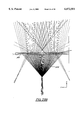
- a conventional liquid crystal display backlight is shown where light from illumination source 1 travels to backlighting light pipe 2 through separate light pipe 3. Separate light pipe 3 is divided into a number of laterally adjacent sections.
- FIG. 2 a partial cross sectional view of the backlighting light pipe 2 in FIG. 1 is shown. The divergence of the incoming light is reduced.
- the present invention includes a generally planar collimating waveguide assembly provided with facets.
- FIG. 4 shows an isometric view of a light engine 90 connected to a waveguide collimator assembly 1000.
- the collimating waveguide assembly can be embodied in several nonmutually exclusive configurations. Subcomponents of these configurations are interchangeable and can be combined.
- light engine 10 is connected to waveguide collimator 25.
- Waveguide collimator 25 is connected to homogenizing diffuser 30.
- Liquid crystal display 40 is connected to diffuser 30.
- Light shaping diffuser 45 is connected to liquid crystal display 40.
- An additional light engine 50 can also be connected to waveguide collimator 25. The order of light shaping diffuser 30 and liquid crystal display 40 can be reversed.
- the liquid crystal display system includes several components. These components can include an illumination source, a reflector, one or more nonimaging optics, a collimating waveguide assembly, a diffuser/homogenizer, a liquid crystal display and a non-Lambertian diffuser.
- these components can include an illumination source, a reflector, one or more nonimaging optics, a collimating waveguide assembly, a diffuser/homogenizer, a liquid crystal display and a non-Lambertian diffuser.
- Equation (42) is a result of Liouvilles' theorem.
- D is the width of the waveguide.
- d is the diameter of the emitter, or source.
- ⁇ is the output angle in air:
- Equation (42) The 90° factor in Equation (42) is based on the fact that light is coming from the source in all directions.
- the optimum light collimating engine, according to Equation (42), provides not only maximum collimation (i.e., minimum angle ⁇ ), but also uniform illumination. Those related designs that are almost optimum are also applicable to this invention.
- the reflector is preferably an extended source arcuate mirror.
- arcuate describes an arc, or curve in 2, or 3, dimensions. Welford.sup.(1) has discussed optimum collimation of light emitted by an extended source, especially spherical and cylindrical sources.
- the optimum design of the reflector is very characteristic of the intended light source and is not actually parabolic. A parabolic shape is actually unsatisfactory for extended sources.
- An arcuate mirror structure can provide an ideal fixture for attachment of the light source to the rest of the structure. As the illumination source moves away from the transformer, optimization of the design of the extended source arcuate mirror reflector increases in importance.
- the waveguide e.g., optical fiber
- the width approaches several millimeters.
- FIG. 7 represents a theoretical construction of a waveguide into which light is being coupled.
- Light which is incident normal to the entry edge of the waveguide passes directly into it without being refracted.
- Light at an angle is refracted.
- low light entering non-normal to the incident surface is collimated.
- the first case scenario light at 90° is coupled at a critical angle of approximately 40° given an index of refraction for the media of 1.55.
- the incident angle in the waveguide ⁇ is equal to approximately 50°. This value is approximately 50° and larger than ⁇ c so all of the light which enters the waveguide collimator is contained within the waveguide collimator by total internal reflection (TIR).
- TIR total internal reflection
- TIR total internal reflection
- 5,390,276 and 5,359,691 realize only one collimation factor, this being collimation from the source via a parabolic reflector, which as discussed above is not of optimum shape for an extended source as broadly discussed in Welford.sup.(1).
- the figures in these patents indicate that the space within the reflector is filled with solid material which zeros the air-material interface collimation factor discussed above.
- Collimation as discussed in U.S. Pat. Nos. 5,359,691 and 5,390,276 is not actually collimation because of the fact that the triangular prisms which are provided only on the bottom of the backlighting light pipe result in a harvesting of only half of the available light.
- Collimating waveguides can be based on either metallic reflection or total internal reflection (TIR).
- TIR total internal reflection
- the waveguide In the first case the waveguide is empty, usually. In the second case the waveguide is material filled.
- TIR total internal reflection
- the second, total internal reflection (TIR) case is better because total internal reflection (TIR) gives exactly 100% reflection while metallic reflection can easily drop to 80% due to surface dirt, contamination.
- Prior art waveguides for this application generally have one metallized side, for backlighting applications, (e.g., U.S. Pat. No. 5,381,309, the entire contents of which are hereby expressly incorporated by reference).
- a transformer is a generalized waveguide structure that not only transmits light through the waveguide but can also change the direction of this light.
- a transformer that changes the direction of light by 90° (orthogonally) can be used to deliberately leak light in a preferred direction for use in an application.
- Prior art patents show several different ways of designing these leaks.
- U.S. Pat. No. 5,390,276 discloses the use of a retroreflecting screen polarizer for further collimating the light in order to illuminate an LCD.
- a major object of the invention is to provide maximum uniform backlighting for an LCD, and at the same time provide light that is highly collimated.
- a diffuser homogenizes light, but in order for the diffuser to operate properly with an LCD, the light reaching the diffuser must be collimated. Collimation begins when the light engine incident rays enter the waveguide. Secondary collimation can occur when the light is taken from the horizontal direction and deflected toward the vertical direction within the waveguide.
- This first description concerns collimation which occurs as the light enters the waveguide from the source.
- One hundred percent collimating efficiency cannot be achieved if the diameter of the source is larger than the diameter of the waveguide.
- the diameter of the source is equal to or less than the diameter of the waveguide optimum efficiency can be approached.
- losses from the mirrors prohibit 100% coupling. Any discussion of 100% coupling therefore implies that the absorptive losses due to interaction of the light with the mirror is being neglected.
- Design of the reflector must be optimized for a particular d/D ratio. Welford.sup.(1) provides ideal designs for any possible ratio. The ideal design means that the Liouville theorem is satisfied. Satisfaction results in 100% being coupled to the waveguide.
- the ideal design also means that the distribution of light within the waveguide will be homogenous. Any of the resulting designs will be quite far from being parabolic.
- a parabolic design is only optimum for a point, or line, source.
- the volume defined by the interior of the reflector can be filled with a media or be simply air. In either case the interior surface of the reflector must be mirrorized (e.g., metallized).
- the reflection efficiency for deep IR and near IR can approach unity, the reflection efficiency for energy within the visible spectra can easily drop to between 90 and 80% due to inefficiency such as dirt on the surface. Maximum reflection efficiency for any wavelength is approximately 96% assuming a metallized mirror surface. In contrast, total internal reflection (TIR) is always 100%.
- the metallic is never 100% even in the IR case.
- the interior of the reflector should be simply air in order to maximize a collimating effect of Snell's law. Even if the diameter of the source is larger than the thickness of the waveguide the worst case 90° incidence light will be collimated to approximately 40°. Deflection design can still be optimized although it will be impossible to reach 100% coupling. Designs for the large laminar situation will be similar to what is shown in FIG. 5 and even further from parabolic.
- the grooves will have variable spacing, ⁇ x. It should be noted that the microgrooves do not need to be continuous. Note that the scattering centers can be separated which is illustrated by the broken lines.
- I 0 represents incident light coming from the left.
- I is the intensity after passing through scaler distance x. Total length of the device is L.
- dx represents an infinitesimally small portion of the scaler distance x.
- FIG. 8 shows a section with dx illustrated. In the general geometry, I is input intensity from the left, reduced to I-dI because dI is leaked to the bottom. This property holds for any coordinate x.
- General Equation (1) indicates that the lost leakage of light-dI must be proportional to I.
- Equation (5) Since a and A are both constant integration yields Equation (5).
- Equation (6) represents that the density of grooves is equal to a constant divided by Equation (5), following directly: ##EQU3## Therefore, ⁇ is a function of x and increases monotonically from P 0 .
- Equation (6B) represents Equation (6C).
- Equation (7) defines a.
- dI/I represents the relative leakage.
- dN is the number of grooves per infinitesimal length.
- a is percentage of leakage per groove.
- Equation (8) represents that intensity at the full length L is 0.
- Equation (8) represents a singularity because the density of ⁇ at the full length L cannot reach infinity. For practical purposes, it can be assumed that no more than 5% of the available light is linked all the way to the end. In addition, a mirror can be placed at the end to reflect the light back toward the source.
- Equation (20) represents the total number of grooves, equal to the length divided by ⁇ x which is the average distance between grooves, ⁇ x: ##EQU7##
- Equation (19) can now be calculated because N T is known.
- Equation (22) represents that a is equal to ##EQU9##
- the average leakage per groove is thus 1.5 ⁇ 10 -3 as represented in Equation (22).
- FIG. 13 illustrates calculation of the groove.
- ⁇ x equals the length of a hypotenuse.
- ⁇ A indicates the angle subtended by the hypotenuse with regard to the base of the waveguide.
- ⁇ c is the total critical (TIR) angle of the light that is within the waveguide, approximately 40°.
- FIG. 13 actually represents a worst case scenario for an extended source, assuming that no collimation was done between the source and its entry into the waveguide.
- ⁇ c is the angle between the incident beam on the reflective surface and the reflective beam, ⁇ c being the maximum divergence within the waveguide.
- Equation (25) represents calculation of ⁇ A based on ⁇ c .
- Equation (25) represents calculation of ⁇ A based on ⁇ c .
- ⁇ A represents the optimum angle for splitting the flux represented by ⁇ c , or other maximum divergence angle, smaller than ⁇ c .
- the typical index of refraction range for the materials of interest is from 1.5 to 1.7, assuming a refractive index of 1.55. These materials include plastics, such as, for example, acrylics such as polymethacrylate and polymethylmethacrylate and other polymers.
- Equation (26) assumes that the exterior medium is air having an index of refraction of 1; ⁇ c is approximately 40° under these conditions. ##EQU11## Thus, ⁇ A equals approximately 35° based on this calculation as shown in Equation (26). Areas are represented in Equation (28), where a is the loss per groove. ##EQU12## Equation (28) represents that a percentage of the flux passing a point is not going to intercept the hypotenuse, based on the hypotenuse being a fraction of the total subtended length between the top of the waveguide and the bottom of the waveguide. Total length of each groove hypotenuse is ⁇ x, assuming that the wave front of the waveguide is homogenous. It should be noted that skew rays are being neglected.
- FIG. 14 shows an imaging collimation slab located beneath a collimating waveguide. A gap of 1 micron between the two slabs is more than sufficient to prevent undesired coupling between the structures, assuming 100 micron lens for example.
- the angle incident upon the collimating imaging optic cannot be smaller than ⁇ c .
- the resulting lens diameter is 2 mm, which is far too large.
- the grooves can be arranged in clusters permitting grouping. By grouping the grooves there can be sufficient spacing for the imaging optics.
- the following example represents an average distance of 2 mm between the clusters of grooves.
- N t represents the number of clusters of grooves.
- ⁇ x is the distance between clusters
- H is the lens diameter
- the size of the grooves can be varied much more and their geometrical position can be cruder, therefore the grooves do not need to be prisms because the spherical rays are subsequently image collimated. Errors from the microgroove surfaces can be accommodated with larger imaging optics.
- the prisms of U.S. Pat. Nos. 5,390,276 and 5,359,691 are acting largely as mirrors and if there is distortion due to imperfect structure the result will be divergence that the structure disclosed in these patents will not subsequently correct for.
- the wedge has a sawtooth pattern. These sawtooths represent a distributed wedge.
- the upper section operates by total internal reflection (TIR) preferably, although the angled facet could be metallized. The determination of the angle in the upper section is based on the same bisectrix that was used to derive the angle of the curved surface. In general it will be appreciated that one facet should be approximately vertical and the other approximately 45° in order to yield a straight-up normal collimated output.
- a monolithic wedge divided into a series of solitudes can be characterized as a distributed wedge.
- Equation (101) is the analog of Equation (1), except that the variable a is a function of x and ⁇ is constant. ##EQU14## Equation (16) is identical to Equation (101) and Equation (17) sets a boundary condition. Equation (118) sets p x a equal to a constant A.
- Equation (123) should be compared to Equation (6).
- Equation (123) a is a function of x whereas in Equation (6) ⁇ is a function of x.
- A is a constant in both equations.
- Equation (123) a is variable where ⁇ is constant.
- the variable a is the leakage rate per microelement.
- Equation (125) Assuming that ⁇ is much less than 1 radian, this ⁇ P is used in the following Equation (125): ##EQU18## Equation (126) describes relative leakage for each event. In the distributed wedge the relative leakage per event is proportional to ⁇ and fitting Equation (123) into Equation (126) yields Equation (128). ##EQU19## In Equation (128), ⁇ is changing with x according to the relationship shown in Equation (132). ##EQU20## As ⁇ increases with x to provide constant leakage, it is enabled to regulate ⁇ . Alternatively, ⁇ can be varied as was previously shown.
- Equation (136) Assuming density is constant at 10 per millimeter, ⁇ is constant as shown in Equation (136), ##EQU21## Assuming a total length L of 20 cm, Equation (137) shows that the leak per grove is small. ##EQU22## Equation (140) shows that the beginning angle only needs to be 1/10th of a degree.
- Equation (128) A more precise version of Equation (128) follows, including a consideration of fresnel reflection, (represented by reflection (intensity coefficient) R as graphically depicted in FIG. 19), and material absorption.
- the power p in Equation (128) is replaced by Equation (300):
- Equation (116) Equation (116) becomes:
- ⁇ 1 and ⁇ 1 the relation between ⁇ and ⁇ is ##EQU24##
- Snell's law has been included.
- ⁇ is the leakage angle and ⁇ is the prism angle. This is shown in Table 1.
- Equation (303) is a transcendental one in such a sense that it cannot be solved analytically.
- an optimized curved surface can be easily designed by assuming homogenous incident flux.
- the bottom of an isosceles pit pyramid is not available to a low incident angle ray.
- constructing an arc instead of a flattened prismatic surface reflecting rays coming from the left requires defining the maximum and minimum angles for those rays which can strike any part of the arc based on the geometry of the waveguide. More specifically, at the top of the arc waves cannot arrive at angles lower than 0° because they would be intercepted by the previous apex.
- the curved tooth facet is mirrored and can be referred to as a vignetting effect where there is a limited size and some parts of the beam are blocked by structures.
- the first facet can be flat. Although it's shown as flat to facilitate analysis of the lowest-most ray, the facet can actually be convex or concave.
- the angular spectrum is very limited. The widest angular spectra is at the top, based on the incoming rays.
- the coordinate system labeled has its origin at the base of the structure. The problem is to find z as a function of x for the curved surface.
- the sawtooth geometry, with curved surface 113 is described, leading to the optimum curved surface z(x).
- This is a curved surface rather than a flat surface because the incident beams at points O, Q, P in FIG. 20, have increasing divergence as illustrated by the hatched areas in FIG. 20.
- FIG. 20 shows tooth 99.
- the vertex 100 of the nonimaging optic(s) (NIO) tooth is O and is positioned following beam collimation optimization according to the Louiville theorem as generally explained by Wilford.sup.(1) and Winston.sup.(2).
- arbitrary point Q 101 has two coordinates (x,z).
- the highest point 102 on the curved wall is P.
- the height of the tooth 103 is taken between P and O.
- the horizontal length of the straight wall is represented by 104.
- the z-coordinate of point Q is represented by 105.
- Point Q is also origin of the coordinate system.
- the lowest angle ( ⁇ ) of incident rays at point Q is represented by 106.
- the highest angle ( ⁇ ) of incident rays at point Q is represented by 107. This is also the maximum angle of beam divergence.
- TIR total internal reflection
- a bisect angle, equal to ##EQU25## is represented by 108.
- Angle 110 is the reflection angle of bisect ray and is equal to angle 109.
- 111 represents the symmetrical angle ( ⁇ ) for bisect rays. It should be noted that symmetrical line 119 is perpendicular to tangential line 114. Therefore, the tangential angle is 90°- ⁇ (or, ⁇ /2- ⁇ ).
- 112 is a straight line (or, wall in cylindrical geometry) of the tooth.
- 113 is the tooth curve that characterizes the optimum NIO profile, minimizing divergence of the output beam. This is because, by contrast to the prism, the ray-bundle at any point at the surface is reflected symmetrically into vertical direction. This is due to the fact that the bisect line of any ray bundle is reflected exactly vertically.
- 114 is the tangential line into the curve at point Q.
- 115 is the incident ray at point O. This is the maximum divergence ray.
- 116 is the lowest inclination ray for the ray bundle at point Q.
- 117 is the highest inclination ray at point Q.
- 118 is the bisect ray for the ray bundle at point Q.
- 119 is the symmetrical line to bisect incident ray 118 and bisect reflected ray 120, which is precisely perpendicular to tangential line 119.
- 120 is the reflected ray into incident bisect ray 118 which is precisely vertical, or parallel to z-axis.
- 121 is the reflected ray to incident ray 115 which is also precisely vertical, according to the optimization principle.
- 122 is the lowest inclination incident at highest Point P, which has a horizontal direction.
- 123 is the highest inclination which is assumed to be ⁇ , in order to accommodate the maximum amount of rays.
- 124 is the bisect ray at point P.
- 125 is the reflected ray to bisect ray 114 which is always precisely vertical, according to the optimization principle.
- Equation (208) can be numerically calculated for various values of G and angles ⁇ .
- FIG. 21 shows a multiplication of the optical element shown in FIG. 20 for uni-directional illumination.
- FIG. 25 is a generalization of FIG. 24 for bi-directional illumination.
- the single sawtooth element from FIG. 22 has been illustrated in detail in FIG. 23 and multiplied in FIG. 24 in order to show a practical sawtooth applied to one side of the collimating waveguide as in FIG. 15.
- the curved surface 113 has been applied on both sides in FIG. 25.
- skew rays have not been considered in this analysis, for simplicity.
- FIG. 26 the structure from FIG. 25 is depicted with smooth lower vertices, in order to minimize the scattering at the edges.
- the shape of the curve in the vignetting effect curved tooth is a function not only of the geometry of the chasm defined by the first facet and the second facet of each optical element but also the output of the light engine. Thus, it is useful to consider the flux dispersion of the light engine and the flux dispersion within the collimating waveguide.
- the collimating waveguides of the present invention can be carried out by using any fabrication method.
- the manufacturing operation it is moreover an advantage to employ a replication/lamination method.
- Isosceles triangles can be cut when fabricating the master for replicating the collimating waveguide provided that there is no undercutting. Any undercutting inhibits mold release. There is a general degradation as you move from the master to the submaster to the finished part. Degradation removes the edges. Much of this degradation is due to the forces exerted during release. Thus, the shape on the master is not necessarily the finished facet structure. Although the facets themselves tend to become convex due to the release process, concave shapes are possible to make. Further, it is relatively easy to combine two facets to define a compound concave structure.
- a metal master can be machined with diamond tooling. Machining flat facet microgrooves with cylindrically variable angles is possible. A spherical or aspheric curve can be cut on a diamond and the resulting curved optical microelement could be as small as 50 microns. Variable angles are possible with curved facets as well. Variable spacing is possible with both flat facets and curved facets. In addition, imaging microlenses can be cut as small as 200 microns. However, the diamond tooling wears-out so it is advantageous to fabricate one master and then replicate a series of submasters.
- Liquid crystal displays can be high definition and/or low definition.
- the number of pixels can be, for example, 2000 ⁇ 2000. Presently the smallest size pixel resolution is approximately 20 microns. These LCDs produce undesirable pixeling effect. Viewers can actually see these pixel demarcations.
- a diffuser located between the collimating waveguide and the LCD is to cancel pixeling effect from the LCD.
- Such a use of a diffuser can be termed homogenizing.
- the directionality of the light emitted from the LCD can be optimized through the use of a diffuser with directional characteristics located on top of the LCD. This would allow a private limited viewing range from a laptop computer.
- Directional diffusers are non-Lambertian diffusers, optical properties of which are defined by planewave response as discussed in U.S. Pat. No. 5,365,354. It can be assumed that the incident waves are not fully collimated but have divergence of perhaps ⁇ 10°. Of course, the divergence from the diffuser cannot be less than the divergence that is reaching it. Typical values would be from approximately 1-40° half angle.
- the output would be approximately the same as the input with regard to divergence.
- Diffusers do not help in collimation.
- diffusers most definitely help in homogenization. Specifically, such diffusers can obviate pixeling from the LCD.
- a diffuser can be located between the groove structure and the LCD structure and/or a diffuser can be located after the LCD. In the former case, the diffuser will homogenize only the grid structure and not the pixels. In the latter case the diffuser would be homogenizing both structures.
- the first step is to create a master diffuser
- the second step is to record in a photosensitive medium with coherent light passed through the master diffuser
- the third step is to replicate the surface structure of the photosensitive medium with, for example, epoxy.
- a fourth and optional step is to make a metal electroform master from the epoxy for mass production purposes. In the alternative, an electroform master may be made directly from the master diffuser.
- a recording set-up 16 comprising a coherent laser light source 18, objective lens 200, master diffuser 22, and photosensitive medium 24.
- Coherent laser light source 18 is standard.
- the objective lens 200 is standard and may be a low or high magnification lens depending upon the desired characteristics of the photosensitive medium 24.
- the objective lens is spaced a distance X from the master diffuser 22.
- the master diffuser 22 may comprise a standard ground glass diffuser, a lenticular diffuser, an acetate diffuser, or a holographic diffuser.
- the ground glass, lenticular, and acetate diffusers are conventional and made in a conventional manner.
- a holographic master diffuser may itself first be recorded in the recording set-up shown in FIG. 18 with the holographic master diffuser to be recorded being positioned at 24 and a conventional ground glass diffuser being located at 22. That master diffuser may then be used to record into another photosensitive medium to be used as a light shaping holographic surface relief diffuser according to the present invention.
- a related set-up for recording volume holographic diffusers is described in U.S. Pat. No. 5,365,354.
- recording a holographic plate with coherent laser light passed through a conventional ground glass diffuser generates features called speckle in the volume of the hologram.
- the size, shape, and orientation of the speckle can be adjusted which in turn affects the angular spread of light scattered from the holographic diffuser upon playback.
- the size of the angular spread of the scattered light in other words, the angular distribution of the scattered light, depends on the average size and shape of the speckle. If the speckle are small, angular distribution will be broad.
- the shape of the angular distribution will be vertically elliptical.
- Speckle size is inversely proportional to the size of the aperture of the master diffuser. If the size of the aperture increases, the size of the speckle decreases and the size of the angular spread of the scattered light from the recorded photosensitive medium increases. Conversely, if the size of the master diffuser aperture decreases, the size of the speckle recorded in the diffuser increases and the angular spread of light scattered from the recorded photosensitive medium decreases. Thus, if the master diffuser aperture is long and narrow, the speckle will be long and narrow as well with their axes oriented perpendicularly to the axis of the aperture. This holds true for both volume holographic recording media as well as surface holographic recording media.
- volume holographic recording media as in U.S. Pat. No. 5,365,354, however, are disclosed there for their volume effect.
- the speckle recorded in the interior or volume of the medium was thought the only desired effect to be obtained from the material.
- DCG volume holographic angular spread
- DCG dichromated gelatin
- the size, shape, and orientation of the surface features recorded in photosensitive medium 24 is a function of a number of variables including the type of objective lens 200 and master diffuser 22 used, as well as the relative positioning of those components with respect to each other and with respect to the photosensitive medium 24. Ultimately, the desired results are obtained through empirical testing. In order to achieve a recorded photosensitive medium having a particular surface structure that can be replicated and comprise a light shaping holographic surface relief diffuser according to the present invention, it may be necessary to adjust the parameters discussed below to achieve the desired shape of the light output.
- the objective lens 200 expands the coherent laser light source 18 so that the area of incidence (or "apparent aperture") of light from the objective lens 200 on the master diffuser 22 is larger than that of the cross section of the laser beam itself.
- the light beam expands in accordance with the magnification of the objective lens 200.
- the aperture of light incident the master diffuser 22 will be smaller than with a large magnification objective lens, such as 60 ⁇ or greater, and therefore the size of the surface features recorded in the photosensitive medium 24 will be larger; the size of the aperture of light incident the master diffuser 22 is inversely related to the size of the surface features recorded in the photosensitive medium 24.
- the distance between the objective lens 200 and the master diffuser 22 must also be taken into account in achieving the desired sculpted surface structure recorded in the photosensitive medium 24.
- the size of the speckle increases. This occurs because as the objective lens 200 moves closer to the master diffuser 22, the apparent aperture of light incident the master diffuser 22 is smaller.
- the size of the speckle recorded in the photosensitive medium 24 is inversely related to the size of the apparent aperture on the master diffuser 22, the speckle will be larger. In turn, the increased speckle size recorded in the photosensitive medium 24 will result in a light shaping holographic surface relief diffuser which has decreased diffusion.
- the apparent aperture of light incident the master diffuser 22 will increase, thus decreasing the size of the speckle recorded in the photosensitive medium 24 and in turn increasing the amount of angular spread of the light shaping holographic surface relief diffuser.
- the distance Y between the master diffuser 22 and the photosensitive medium 24 also affects speckle size.
- the size of the speckle recorded in the photosensitive medium 24 decreases as well. This occurs because, assuming an expanded beam of light is produced at objective lens 200, as the photosensitive medium 24 is moved closer to the master diffuser 22, the light beam emanating from each of the irregularities in the master diffuser 22 will expand less by the time it reaches the photosensitive medium 24, thus producing smaller speckle.
- the distance Y is increased, the size of the speckle recorded will be increased.
- Predefined output areas that are "off-axis" with respect to the normal axis of the diffuser are achieved by tilting the photosensitive medium 24 around an axis normal to its surface.
- a 20° off axis diffuser may be achieved by fitting the photosensitive medium 24 roughly 20°.
- the shape of the speckle recorded in photosensitive medium 24 will be roughly round as will the shape of the angular output of a light shaping holographic surface relief diffuser made from photosensitive medium 24.
- a round output may also be achieved when a lenticular or an acetate sheet is used as a master diffuser 22.
- Lenticular sheets have tiny lens-like elements machined in them.
- Acetate diffusers are made by an extrusion and embossing process which also yields roughly round speckle. It is difficult to create or control the desired irregularities in acetate diffusers. With respect to lenticular diffusers, the surface effects necessary to achieve varying output shapes are complex machined macroscopic structures.
- a prerecorded holographic master diffuser is used as the master diffuser 22 as the master diffuser 22 as the master diffuser 22
- additional degrees of recording freedom are achieved because the master diffuser can be prerecorded with speckle having virtually any shape, size, and orientation as discussed further below. Speckle characteristics are more easily controlled using a holographic master diffuser.
- the master diffuser in the recording set-up in FIG. 18, the master diffuser must be able to transmit light so that it reaches the photosensitive medium 24 from the objective lens 200.
- a substrate is needed as part of the master diffuser 22, such as if a holographic master diffuser is used, the substrate should be capable of efficiently transmitting light.
- a glass substrate is preferable.
- holographic master diffusers are preferable because better uniformity of intensity in the photosensitive medium 24 is achieved, higher transmission efficiency through the master diffuser 22 is achieved, and the holographic master diffuser 22 causes less back scatter than a ground glass diffuser.
- a first generation holographic volume master diffuser may be made using a ground glass or acetate diffuser. This holographic diffuser can then be used to make a second generation holographic master diffuser, either volume or surface with greater control.
- light source 60 is located within space defined by mirror 70.
- Light source 60 can be a cold cathode fluorescent bulb or a hot cathode fluorescent bulb.
- Light from light source 60 is directed toward waveguide collimator 80.
- Light source 60 is connected to mirror 70 through fixture 90.
- Waveguide collimator 80 includes incident end 130.
- the bottom of waveguide collimator 80 is provided with a first plurality of substantially parallel optical elements 140.
- Each of the first plurality of substantially parallel optical elements 140 includes a first facet 142 and a mirrored second facet 144.
- Waveguide collimator 80 includes a top surface 146.
- Waveguide collimator 80 can also include a reflective end (not shown).
- Light engine 1100 is connected to waveguide collimator assembly 108.
- Light source 1200 is a linear array of light emitting diodes connected to a metallized mirror that is part of light engine 1100.
- light from the illumination source can be directly incident upon the incident end. This means that there is no structure between the illumination source and the incident end. For example, the space between the illumination source and the incident end should be occupied by air, or vacuum. By the absence of any structure between the illumination source and the incident end, a higher degree of collimation is achieved when light passes through the incident end in accordance with Snell's law.
- first distributed wedge collimating waveguide 150 includes a first plurality of substantially parallel optical elements 160. Each of this first plurality of substantially parallel optical elements 160 includes a mirrored first facet 162 that can be substantially flat and a second facet 164 that can be substantially flat. First distributed wedge collimating waveguide 150 also includes top surface 166. The angle ⁇ which is defined as the angle that the mirrored first facet 162 makes with the top surface 166 should be optimized. Second distributed collimating waveguide 170 is optically connected to first distributed wedge collimating waveguide 150. Second distributed wedge collimating waveguide 170 includes upper surface 172. First diffuser 180 for homogenizing light from top surface 172 is optically connected to second distributed wedge collimating waveguide 170.
- An additional collimating waveguide including a plurality of imaging optics can be located between first diffuser 180 and second distributed wedge collimating waveguide 170.
- a diffuser can be located adjacent incident end 168.
- FIG. 12 shows a ray diagram for the apparatus depicted in FIG. 11.
- a ray is leaked at near zero degree angle to the top surface. It will be appreciated that this ray is emitted from the top of the diffuser toward the left.
- a ray is emitted from the top surface at an angle ⁇ . This ray emerges normal to the plane defined by the diffuser.
- a ray emerges from the top surface at an angle to ⁇ . It will be appreciated that this ray is emitted from the diffuser toward the right.
- first collimating waveguide 190 is provided with a first plurality of substantially parallel optical elements 195.
- Each of the first plurality of substantially parallel optical elements 195 includes a mirrored first facet 197 and a second facet 198.
- First collimating waveguide includes a top surface 196 and an incident end (not shown).
- Second collimating waveguide 210 is optically connected to the top surface 196.
- Second collimating waveguide 210 is provided with a plurality of substantially parallel imaging optics 220.
- Second collimating waveguide 210 includes upper surface 215.
- first collimating waveguide 230 includes top surface 231.
- First collimating waveguide 230 also includes an incident end (not shown) and a reflective end (not shown).
- First collimating waveguide 230 is provided with a first plurality of substantially parallel optical elements 240.
- Each of the first plurality of substantially parallel optical elements 240 includes a first facet 242 and a mirrored second facet 244.
- Second facet 244 is concave with respect to top surface 231.
- first facet 242 can also be concave with respect to top surface 231.
- first facet 242 is equivalent to the angular dispersion of the rays incident upon mirrored second facet 244 at the point being considered.
- the aspect ratio of the base of the elements is proportional to the ratio of divergence of the beams in horizontal and vertical.
- a first plurality of substantially parallel optical elements having concave facets have been replicated in a first collimating waveguide. It will be appreciated that the first plurality of substantially parallel optical elements are not continuous but rather have been segmented into a series of microchasms.
- a second plurality of substantially parallel imaging optics are shown replicated in a second collimating waveguide. It will be appreciated that the second plurality of substantially parallel optical elements have been segmented into spherically symmetric indentations.
- a first plurality of substantially parallel optical elements formed in a first collimating waveguide is shown.
- the first plurality of substantially parallel optical elements have mirrored first facets that are concave and mirrored second facets that are concave. It will be appreciated that concavity of the facets has been three dimensionally deviated so as to define scalloped edges so as to collimate skew rays.
- one light source is often preferred. This also allows for a more compact structural design.
- the use of two sources can be conjunctively combined with an optical element having opposed concave surfaces so as to preferentially direct flux upward where the flux is incident from both sides of the waveguide collimator.
- This opposed concave configuration is also applicable to the case where one light source is used in conjunction with a mirror on the reflective end of the collimating waveguide.
- a symmetrical identical backside is preferred. This will also effectively collimate much of the backscattered light.
- the back surface can be concave in a different configuration from the front surface.
- a liquid crystal display backlighting system can be based on a collimating waveguide 300 and a light bending and viewing film 400.
- the collimating waveguide 300 can function based on mirror reflection and/or total internal reflection.
- the collimating waveguide 300 is connected to a lamp 310 and a reflector 320.
- Light from the lamp 310 is conducted through an angular filtering film 330 to a nonimaging optic(s) (NIO) 340.
- the angular filtering film 330 includes a flat side 321 and a second side 322 having a plurality of parallel isometric triangular prisms, or a 2d array of prisms as shown in FIGS. 33A-33C.
- the function of the angular filtering film 330 is to collimate light are reject stray rays.
- NIO 340 can be a light pipe with rectilinear top and bottom surfaces, as shown, or a collimating waveguide with slanting top and bottom surfaces.
- the nonimaging optic 340 can be connected to, or formed integrally with, collimating waveguide 300.
- the invention is preserved even if one or more of the reflector 320, the angular filtering film 330 and the NIO 340 are omitted, these elements being optional.
- each of a first plurality of optical elements 350 formed at the bottom of the collimating waveguide 300 can have two planar facets, one planar facet and one curved facet, or two curved facets.
- each of the first of the plurality of optical element has a first flat facet 351 and a second flat facet 352, the later of which is designed to function by total internal reflection (TIR).
- each of the first plurality of optical elements has a flat facet and a concave curved facet, the later of which is designed to function by total internal reflection (TIR).
- One, both or none of the facets of the plurality of optical elements 350 can be designed to function by total internal reflection, or alternatives including metallic reflection, absorption and/or transmission.
- the light rays 361-362 that are output from collimating waveguide 300 via second flat facet 352 are confined within a relatively narrow angular range that is non-normal to the top surface of collimating waveguide 300.
- the invention includes embodiments where the output angular range is normal to the top surface.
- an underlayer 360 can be located beneath the first plurality of optical elements 350.
- the underlayer 360 can be a separate flexible layer of reflective material such as, for example, Imperial Chemical Industries (ICI) Melinex #329-500.
- the underlayer 360 improves both the efficiency of brightness and the cosmetics of the system.
- the underlayer 360 can be completely opaque, substantially opaque or partially transmissive.
- the underlayer 360 can be white, pearlescent or colored.
- the system can include an LCD (not shown) located above the illustrated subassembly. The function of the LCD is to provide a laptop computer, or other, display.
- Light bending and view film 400 includes a second plurality of optical elements 410.
- Each of the second plurality of optical elements 410 has a first flat facet 411 and a second flat facet 412, the later of which is designed to function by TIR.
- Each of the second plurality of optical elements 410 can have two flat facets, one flat facet and one curved facet, or two curved facets.
- two, one or none of the facets can be designed to function by TIR, or alternatives including metallic reflection, absorption and/or transmission.
- the second facet functions by TIR and is concave with respect to the first facet.
- the light that is output from collimating waveguide 300 is refracted upon entry into the light bending and viewing film 400 after traveling between the top surface of collimating waveguide 300 and the first facet 411 of the second plurality of optical elements 410.
- the refracted light then undergoes TIR by the second facet 412 of the second plurality of optical elements 410.
- this reflection could be mirrored reflection due to, for example, a metalization layer, or absorption by a coating, or transmission, in addition to the depicted total internal reflection.
- the reflected light from second facet 412 then travels toward a surface diffuser 420.
- the surface diffuser 420 can be an integral part of film 400 or be a separate layer that is laminated, or otherwise, attached to film 400.
- the material in which the surface diffuser is replicated or molded can have the same index of refraction as the rest of film 400, even if it is not an integral part thereof.
- the light that is output from the light bending and viewing film 400 via surface diffuser 420 can be shaped into a relatively narrow angular range or dispersed into a relatively wide angular range.
- the light that is output via surface diffuser 420 can be normal or non-normal to the top of light bending and viewing film 400. In the depicted embodiment of FIG. 27A, the output light widely dispersed and non-normal to the average top surface of surface diffuser 420.
- the light bending and viewing film 400 can be a single layer of material that includes a lower topography 426 that defines the second plurality of optical elements and an upper topography 428 that defines the surface diffluser.
- light bending and viewing film 400 can be a two, or three, or even more, layer composite material.
- the second plurality of optical elements can be replicated in a first layer of photopolymerizable material that is provided on one side of a polyester carrier web.
- the surface diffuser can be replicated in a second layer of photopolymerizable material that is proved on the other side of the polyester carrier web, thereby embedding the web between the two photopolymerized layers.
- the carrier web can be simultaneously provided with opposing photopolymerizable material layers that are simultaneously replicated and polymerized.
- one of the topographies can be compression molded to form a layer that acts as a carrier for a coating of photopolymerizable material into which the second topography is replicated.
- both topographies of film 400 can be embossed onto a single layer of polycarbonate or other suitable material, or injection molded.
- FIG. 28A the ray tracings are shown for light that is being emitted from a localized source. More specifically, in FIG. 28A, a plurality of light rays are illustrated emanating from a virtual point source to depict an elementary response of film 400.
- a light bending and turning film 910 includes a lower topography 926 that defines a plurality of optical elements and an upper topography 928 that defines a surface diffuser 929.
- a collimating waveguide 950 is located near the lower topography 926. It will be appreciated that many of the rays illustrated within waveguide 950 are being reflected by TIR and are not reaching the lower topography 926. Thus, the rays that do emerge are fairly well collimated. Further, referring to a series of rays 931, 932, and 933, it will also be appreciated that the film 910 functions to further collimate the light that enters the film 910 through the lower topography 926.
- an angular filtering film 500 (e.g., BEF available from 3M of Minnesota, can be located adjacent the light engine inlet end of a collimating waveguide (not shown). It should be noted that film 500 cannot properly be termed a brightness enhancing film because such an effect is contrary to the second law of thermodynamics. The phrase angular filtering film is more precise.
- Angular filtering film 500 can include a flat side 510 and a second side 520 having a plurality of isometric triangular prisms 530. A portion of any incident light, represented by the downward pointing arrowhead 555, is collimated by film 500.
- film 500 acts as a collimating structure for some rays and simultaneously as a rejection filter for other rays, depending on incident position of these rays with regard to the triangular prism apexes 535. For example, rays 541, 542, 543, and 544 are being rejected by the film 500 are returned back toward the top of the figure.
- FIG. 29B a larger number of rays interacting with a film 500 are shown. It will be appreciated that only a fraction of the incident rays 525 will be directed toward the LCD (not shown).
- FIGS. 33A, 33B, and 33C three alternative angular filtering films that provide at least some degree of 3D filtering, in addition to the usual 2d filtering provided by such structures, are depicted.
- a planar array of pyramids 560 is shown in FIG. 33A.
- a planar array of extended pyramidal structures 570 is shown in FIG. 33B.
- a planar array of cones 580 is shown in FIG. 33C. All three of these embodiments provide some degree of angular filtering in the Z direction, as well as in the X and Y directions.
- a liquid crystal display backlighting system 600 can be based on a collimating waveguide 605 that is configured for use with a first light source 610 and a second light source 620.
- a plurality of optical elements 606 formed at the bottom of collimating waveguide 605 are progressive in shape and symmetrically arranged with regard to a centerline of collimating waveguide 605.
- the geometries of the facets of the plurality of optical elements 606 can be configured so as to operate by mirrored reflection or by total internal reflection.
- Opaque pearlescent underlayer 616 improves efficiency.
- Underlayer 616 can be a separate layer of material that is spaced apart from the bottom of collimating waveguide 605 or a surface that is adjacent the plurality of optical elements 606.
- one, or both, of the light sources can be a stack of two, or more, lamps.
- Each individual light source may, or may not include a barrier 618 that acts a screening aperture to prevent stray light from illuminating the LCD (not shown in FIG. 30) from unintended angles.
- the first light source 610 is a stack of two lamps having a twin extended source arcuate reflector 609.
- First light source 610 is connected to collimating waveguide 605 with an angular filtering film 611 and a solid nonimaging optics 612.
- the second light source 620 has a twin parabolic reflector 619 and is directly connected to collimating waveguide 605 without any intervening NIO.
- the intervening structure, NIO 612, and the reflectors 609 and 619 can all be referred to using a broad definition of NIO).
- FIG. 30 is not the only permutation of elements that can be assembled according to the invention.
- the totality of embodiments includes a large number of embodiments.
- a light turning and viewing film 700 can include a plurality of optical elements 710, each of which has a flat facet 720 and a curved facet 730.
- the curved facets can be identical or optimized with regard to the flux that is expected to be reflected by that facet.
- flat facet 720 is transparent and curved facet 730 functions by total internal reflection.
- the second facet can be flat and/or metallized so as to operate by mirrored reflection.
- a collimating waveguide 800 can include a plurality of optical elements 810, each of which has a curved facet 820 that is optimized with regard to the flux that is expected to be reflected by that facet.
- Each of the plurality of optical elements 810 also includes a flat facet 830.
- Curved facet 820 can function by total internal reflection or be provided with a reflective coating so as to function by mirrored reflection. These reflective facets can be flat or curved. While the illustrated collimating waveguide is configured for use with a single illumination source provided at one end, if two illumination sources are provided at opposing ends of the waveguide, both of the facets of the plurality of optical elements can operate to reflect light upwards.
- the facets of the plurality of optical elements can be fabricated so as to use any combination of mirrored and/or total internal reflection surfaces as well as any combination of flat and/or curved surfaces.
- the curved facets become shorter as you move away from a light source at the left of the drawing, (not shown).
- the upper vertex angle between the flat facets and the corresponding curved facets, as well as the curve shape are constant, but the flat facet angle increases as you move away from the light source.
- the depth of the grooves decreases with distance away from the light source.
- This topography can be replicated using a master in which each of the plurality of optical elements is sequentially cut with a diamond tool that is incrementally rotated with regard to the previous element.
- Preferred embodiments of the present invention can be identified one at a time by testing for the presence of collimated output.
- the test for the presence of collimated output can be carried out without undue experimentation by the use of simple and conventional polarization experiments.
- guidance toward the next preferred embodiment can be based on the presence of homogeneity.
- the disclosed embodiments show a fluorescent bulb as the structure for performing the function of emitting light, but the structure for emitting light can be any other structure capable of performing the function of emitting light, including, by way of example an array of light emitting diodes (LEDs), or any other non-monochromatic light source, such as a strobe light.
- the illumination source can even be a monochromatic light source, albeit less commercially viable.
- the disclosed embodiments show cylindrical and conical microlenses as the structures for performing the function of imaging collimation, but the structure for imaging collimation can be any other structure capable of performing the function of changing the divergence light, including, by way of example a nonlinear optic such as a convection chamber.
- the disclosed embodiments show a light shaping diffuser as the structure for performing the function of shaping light, but the structure for shaping light can be any other structure capable of performing the function of shaping light, including, by way of example, a lens such as a Fresnel lens.
- a practical application of the present invention which has value within the technological arts is illuminating a liquid crystal display. Further, all the disclosed embodiments of the present invention are useful in conjunction with liquid crystal displays such as are used for the purpose of displaying data, or for the purpose of displaying an image, or the like. There are virtually innumerable uses for the present invention described herein, all of which need not be detailed here.
- the present invention described herein provides substantially improved results that are unexpected in that a very good output is obtained with relatively low power.
- the present invention described herein can be practiced without undue experimentation. The entirety of everything cited above or below is hereby expressly incorporated by reference.
- the compactness of the system could be enhanced by providing thinner illumination sources or thinner collimating waveguides.
- plastic is preferred for the collimating waveguide, any optically refractive material could be used in its place.
- the rest of the individual components need not be fabricated from the disclosed materials, but could be fabricated from virtually any suitable materials.
- the individual components need not be formed in the disclosed shapes, or assembled in the disclosed configuration, but could be provided in virtually any shape, and assembled in virtually any configuration, which collimate light so as to provide backlighting.
- the liquid crystal display system described herein is a physically separate module, it will be manifest that the liquid crystal display may be integrated into the apparatus with which it is associated.
- all the disclosed features of each disclosed embodiment can be combined with, or substituted for, the disclosed features of every other disclosed embodiment except where such features are mutually exclusive.
Priority Applications (6)
| Application Number | Priority Date | Filing Date | Title |
|---|---|---|---|
| US08/782,962 US6072551A (en) | 1996-02-14 | 1997-01-13 | Backlight apparatus for illuminating a display with controlled light output characteristics |
| DE69728754T DE69728754T2 (de) | 1996-02-14 | 1997-02-12 | Gerät zur rückseitigen beleuchtung einer flüssigkristallanzeigevorrichtung |
| JP9529460A JP2000504855A (ja) | 1996-02-14 | 1997-02-12 | 液晶ディスプレイバック照明装置 |
| PCT/US1997/002226 WO1997030373A1 (en) | 1996-02-14 | 1997-02-12 | Apparatus for lcd backlighting |
| CA002245833A CA2245833C (en) | 1996-02-14 | 1997-02-12 | Apparatus for lcd backlighting |
| EP97906909A EP0880723B1 (de) | 1996-02-14 | 1997-02-12 | Gerät zur rückseitigen beleuchtung einer flüssigkristallanzeigevorrichtung |
Applications Claiming Priority (2)
| Application Number | Priority Date | Filing Date | Title |
|---|---|---|---|
| US08/601,133 US5838403A (en) | 1996-02-14 | 1996-02-14 | Liquid crystal display system with internally reflecting waveguide for backlighting and non-Lambertian diffusing |
| US08/782,962 US6072551A (en) | 1996-02-14 | 1997-01-13 | Backlight apparatus for illuminating a display with controlled light output characteristics |
Related Parent Applications (1)
| Application Number | Title | Priority Date | Filing Date |
|---|---|---|---|
| US08/601,133 Continuation-In-Part US5838403A (en) | 1996-02-14 | 1996-02-14 | Liquid crystal display system with internally reflecting waveguide for backlighting and non-Lambertian diffusing |
Publications (1)
| Publication Number | Publication Date |
|---|---|
| US6072551A true US6072551A (en) | 2000-06-06 |
Family
ID=27083796
Family Applications (1)
| Application Number | Title | Priority Date | Filing Date |
|---|---|---|---|
| US08/782,962 Expired - Lifetime US6072551A (en) | 1996-02-14 | 1997-01-13 | Backlight apparatus for illuminating a display with controlled light output characteristics |
Country Status (6)
| Country | Link |
|---|---|
| US (1) | US6072551A (de) |
| EP (1) | EP0880723B1 (de) |
| JP (1) | JP2000504855A (de) |
| CA (1) | CA2245833C (de) |
| DE (1) | DE69728754T2 (de) |
| WO (1) | WO1997030373A1 (de) |
Cited By (57)
| Publication number | Priority date | Publication date | Assignee | Title |
|---|---|---|---|---|
| US6285426B1 (en) * | 1998-07-06 | 2001-09-04 | Motorola, Inc. | Ridged reflector having optically transmissive properties for an optical display device |
| US6285425B1 (en) * | 1998-06-29 | 2001-09-04 | Motorola, Inc. | Ridged reflector for an optical display having a curved and a planar facet for each ridge |
| US6356391B1 (en) * | 1999-10-08 | 2002-03-12 | 3M Innovative Properties Company | Optical film with variable angle prisms |
| WO2002070990A1 (en) * | 2001-03-05 | 2002-09-12 | Universita' Degli Studi Di Roma 'la Sapienza' | Astronomical, particularly solar and/or lunar, goniometric indicator |
| US6553133B1 (en) * | 1999-09-22 | 2003-04-22 | U.T. Battelle, Llc | Four-dimensional characterization of a sheet-forming web |
| WO2003036162A1 (en) * | 2001-10-24 | 2003-05-01 | Koninklijke Philips Electronics N.V. | Optical element with foil held by underpressure, method of manufacture, and display unit with such element |
| US20030128399A1 (en) * | 2001-11-06 | 2003-07-10 | Fuji Photo Film Co., Ltd. | Image transfer apparatus |
| EP1348994A1 (de) * | 2000-12-13 | 2003-10-01 | Mitsubishi Rayon Co., Ltd. | Lichtquelleneinrichtung |
| US6652109B2 (en) * | 2000-12-14 | 2003-11-25 | Alps Electric Co., Ltd. | Surface light emission device, method of manufacturing the same, and liquid crystal display device |
| EP1418458A1 (de) * | 2002-11-06 | 2004-05-12 | Samsung Electronics Co., Ltd. | Am Kopf montierte Anzeige mit direkter Netzhautprojektion |
| US20050286262A1 (en) * | 2004-06-24 | 2005-12-29 | Jean-Claude Gasquet | Lighting and/or signalling device with optical guide |
| US20060009749A1 (en) * | 2004-02-19 | 2006-01-12 | Weckwerth Mark V | Efficient diffuse light source assembly and method |
| US20060045144A1 (en) * | 2004-09-01 | 2006-03-02 | Nlight Photonics Corporation | Diode laser array beam homogenizer |
| US20060083508A1 (en) * | 2004-03-11 | 2006-04-20 | Canon Kabushiki Kaisha | Illumination apparatus and photographing apparatus having the same |
| US20060120111A1 (en) * | 2004-12-02 | 2006-06-08 | Yasunori Onishi | Illumination device and light guide plate |
| US20070032847A1 (en) * | 2003-02-25 | 2007-02-08 | Spectragenics, Inc. | Self-contained, diode-laser-based dermatologic treatment apparatus |
| US20070297051A1 (en) * | 2004-07-06 | 2007-12-27 | Yu Huang | Total internal reflection fresnel lens systems, assemblies, and methods |
| US20080027518A1 (en) * | 2003-02-25 | 2008-01-31 | Spectragenics, Inc. | Self-contained, eye-safe hair-regrowth-inhibition apparatus and method |
| US20080271776A1 (en) * | 2007-05-01 | 2008-11-06 | Morgan Solar Inc. | Light-guide solar panel and method of fabrication thereof |
| US20090046220A1 (en) * | 2006-02-01 | 2009-02-19 | Harison Toshiba Lighting Corporation | Backlight for liquid crystal display device |
| US20090064993A1 (en) * | 2007-09-10 | 2009-03-12 | Banyan Energy, Inc. | Solar energy concentrator |
| US20090067784A1 (en) * | 2007-09-10 | 2009-03-12 | Banyan Energy, Inc. | Compact optics for concentration, aggregation and illumination of light energy |
| US20090125006A1 (en) * | 2004-02-25 | 2009-05-14 | Spectragenics, Inc. | Optical Sensor and Method for Identifying the Presence of Skin |
| US20090204109A1 (en) * | 2003-02-25 | 2009-08-13 | Tria Beauty, Inc. | Eye-Safe Dermatologic Treatment Apparatus and Method |
| US20100069898A1 (en) * | 2003-02-25 | 2010-03-18 | Tria Beauty, Inc. | Acne Treatment Method, System and Device |
| US20100231498A1 (en) * | 2009-03-13 | 2010-09-16 | Microsoft Corporation | Image display via multiple light guide sections |
| WO2010114586A1 (en) * | 2009-04-03 | 2010-10-07 | Vuzix Corporation | Beam segmentor for enlarging viewing aperture of microdisplay |
| WO2010124028A2 (en) * | 2009-04-21 | 2010-10-28 | Vasylyev Sergiy V | Light collection and illumination systems employing planar waveguide |
| US20110011449A1 (en) * | 2007-05-01 | 2011-01-20 | Morgan Solar Inc. | Light-guide solar panel and method of fabrication thereof |
| US20110044579A1 (en) * | 2009-08-21 | 2011-02-24 | Microsoft Corporation | Efficient collimation of light with optical wedge |
| US20110043142A1 (en) * | 2009-08-21 | 2011-02-24 | Microsoft Corporation | Scanning collimation of light via flat panel lamp |
| US20110261292A1 (en) * | 2008-12-12 | 2011-10-27 | Shenzhen Tcl New Technology Ltd. | System and method for decreasing the power requirements of a backlight for a liquid crystal display |
| US8328403B1 (en) | 2012-03-21 | 2012-12-11 | Morgan Solar Inc. | Light guide illumination devices |
| US8412010B2 (en) | 2007-09-10 | 2013-04-02 | Banyan Energy, Inc. | Compact optics for concentration and illumination systems |
| US8705914B2 (en) | 2007-09-10 | 2014-04-22 | Banyan Energy, Inc. | Redirecting optics for concentration and illumination systems |
| US8854799B2 (en) | 2012-03-02 | 2014-10-07 | Microsoft Corporation | Flux fountain |
| US8873227B2 (en) | 2012-03-02 | 2014-10-28 | Microsoft Corporation | Flexible hinge support layer |
| US8885995B2 (en) | 2011-02-07 | 2014-11-11 | Morgan Solar Inc. | Light-guide solar energy concentrator |
| US8947353B2 (en) | 2012-06-12 | 2015-02-03 | Microsoft Corporation | Photosensor array gesture detection |
| US9075566B2 (en) | 2012-03-02 | 2015-07-07 | Microsoft Technoogy Licensing, LLC | Flexible hinge spine |
| US9201185B2 (en) | 2011-02-04 | 2015-12-01 | Microsoft Technology Licensing, Llc | Directional backlighting for display panels |
| US9256089B2 (en) | 2012-06-15 | 2016-02-09 | Microsoft Technology Licensing, Llc | Object-detecting backlight unit |
| US9337373B2 (en) | 2007-05-01 | 2016-05-10 | Morgan Solar Inc. | Light-guide solar module, method of fabrication thereof, and panel made therefrom |
| US9354748B2 (en) | 2012-02-13 | 2016-05-31 | Microsoft Technology Licensing, Llc | Optical stylus interaction |
| EP3034935A1 (de) * | 2014-12-15 | 2016-06-22 | Samsung Electronics Co., Ltd | Rückbeleuchtungsvorrichtung und anzeigevorrichtung damit |
| US9552777B2 (en) | 2013-05-10 | 2017-01-24 | Microsoft Technology Licensing, Llc | Phase control backlight |
| US20170082269A1 (en) * | 2013-03-15 | 2017-03-23 | Cree, Inc. | Optical Components for Luminaire |
| US9687671B2 (en) | 2008-04-25 | 2017-06-27 | Channel Investments, Llc | Optical sensor and method for identifying the presence of skin and the pigmentation of skin |
| US9824808B2 (en) | 2012-08-20 | 2017-11-21 | Microsoft Technology Licensing, Llc | Switchable magnetic lock |
| US9870066B2 (en) | 2012-03-02 | 2018-01-16 | Microsoft Technology Licensing, Llc | Method of manufacturing an input device |
| US9958601B2 (en) | 2013-09-19 | 2018-05-01 | University Of Utah Research Foundation | Display backlight |
| US10082669B2 (en) | 2011-07-27 | 2018-09-25 | Microsoft Technology Licensing, Llc | Variable-depth stereoscopic display |
| US10120420B2 (en) | 2014-03-21 | 2018-11-06 | Microsoft Technology Licensing, Llc | Lockable display and techniques enabling use of lockable displays |
| US10324733B2 (en) | 2014-07-30 | 2019-06-18 | Microsoft Technology Licensing, Llc | Shutdown notifications |
| US10678743B2 (en) | 2012-05-14 | 2020-06-09 | Microsoft Technology Licensing, Llc | System and method for accessory device architecture that passes via intermediate processor a descriptor when processing in a low power state |
| US10809442B2 (en) * | 2014-12-16 | 2020-10-20 | Saturn Licensing Llc | Light emitting device, display unit, and illumination unit |
| US20220029063A1 (en) * | 2020-07-27 | 2022-01-27 | Lextar Electronics Corporation | Optical film and light emitting device including the same |
Families Citing this family (18)
| Publication number | Priority date | Publication date | Assignee | Title |
|---|---|---|---|---|
| US6712481B2 (en) * | 1995-06-27 | 2004-03-30 | Solid State Opto Limited | Light emitting panel assemblies |
| DE69738551T2 (de) * | 1997-09-19 | 2009-04-02 | Teledyne Lighting and Display Products, Inc., Hawthorne | Auskopplung von Licht aus einem optischen Wellenleiter mit hohem Wirkungsgrad durch Holographisch erzeugte Lichtstreumittel |
| JP2001194534A (ja) | 2000-01-13 | 2001-07-19 | Nitto Denko Corp | 導光板及びその製造方法 |
| KR100769779B1 (ko) | 2000-01-13 | 2007-10-24 | 닛토덴코 가부시키가이샤 | 광학 필름 및 액정 디스플레이 장치 |
| EP1143269B1 (de) | 2000-01-13 | 2007-03-14 | Nitto Denko Corporation | Polarisator zur Änderung des optischen Wegs |
| JP4442836B2 (ja) | 2000-02-02 | 2010-03-31 | 日東電工株式会社 | 光学フィルム |
| JP4609962B2 (ja) | 2000-02-02 | 2011-01-12 | 日東電工株式会社 | 光学フィルム |
| JP2001228315A (ja) | 2000-02-14 | 2001-08-24 | Nitto Denko Corp | 反射板及び液晶表示装置 |
| DE10018284A1 (de) * | 2000-04-13 | 2001-10-18 | Valeo Beleuchtung Deutschland | Signalleuchte mit mindestens einem Leuchtmittel und einem Lichtleiter |
| JP2002131552A (ja) | 2000-10-24 | 2002-05-09 | Nitto Denko Corp | 導光板、面光源装置及び反射型液晶表示装置 |
| JP4662402B2 (ja) | 2001-03-12 | 2011-03-30 | 日東電工株式会社 | 外光及び照明両モード用のフロントライト用の導光板、外光及び照明両モード用のフロントライト用の面光源装置並びに外光及び照明両モード用のフロントライト式の反射型液晶表示装置 |
| US7345824B2 (en) * | 2002-03-26 | 2008-03-18 | Trivium Technologies, Inc. | Light collimating device |
| US7293906B2 (en) * | 2005-05-23 | 2007-11-13 | Avago Technologies Ecbu Ip (Singapore) Pte Ltd | Light source adapted for LCD back-lit displays |
| KR100673990B1 (ko) * | 2005-05-24 | 2007-01-25 | 엘지전자 주식회사 | 백라이트 유닛, 액정 표시 장치 및 이에 사용되는 역프리즘시트 |
| JP4307477B2 (ja) | 2006-07-04 | 2009-08-05 | 三星モバイルディスプレイ株式會社 | 導光板およびバックライトユニット |
| EP2385904A1 (de) | 2009-01-08 | 2011-11-16 | 3M Innovative Properties Company | Trockener löschbarer projektionsartikel und system |
| CN102667618B (zh) | 2009-11-23 | 2015-02-25 | 3M创新有限公司 | 具有高对比度的正投影屏幕 |
| US20140347571A1 (en) * | 2013-05-24 | 2014-11-27 | Raytheon Company | Low profile backlight apparatus for high-brightness microdisplays |
Citations (60)
| Publication number | Priority date | Publication date | Assignee | Title |
|---|---|---|---|---|
| US4099172A (en) * | 1975-07-11 | 1978-07-04 | Ing. C. Olivette & C., S.P.A. | Electronic visual display unit for alphanumeric characters |
| US4140378A (en) * | 1975-08-09 | 1979-02-20 | Canon Kabushiki Kaisha | View finder device having liquid crystal cell |
| US4299462A (en) * | 1975-08-09 | 1981-11-10 | Canon Kabushiki Kaisha | View finder device having liquid crystal cell |
| US4344686A (en) * | 1977-10-19 | 1982-08-17 | Agfa-Gevaert Aktiengesellschaft | Photographic camera with state-of-focus indication |
| US4431260A (en) * | 1979-02-26 | 1984-02-14 | General Dynamics, Pomona Division | Method of fabrication of fiber optic coupler |
| JPS59226303A (ja) * | 1983-06-07 | 1984-12-19 | Seiko Epson Corp | 平面光源 |
| US4497860A (en) * | 1978-12-18 | 1985-02-05 | Minnesota Mining And Manufacturing Company | Imageable prismatic array |
| JPS6411203A (en) * | 1987-07-03 | 1989-01-13 | Dai Ichi Seiko Co Ltd | Lighting device |
| US4906070A (en) * | 1985-11-21 | 1990-03-06 | Minnesota Mining And Manufacturing Company | Totally internally reflecting thin, flexible film |
| US4917465A (en) * | 1989-03-28 | 1990-04-17 | In Focus Systems, Inc. | Color display system |
| US4963016A (en) * | 1986-03-18 | 1990-10-16 | U.S. Philips Corporation | Compact rear-projection system with obliquely incident light beam |
| US4975808A (en) * | 1989-10-02 | 1990-12-04 | Motorola, Inc. | Backlighting apparatus |
| US4989948A (en) * | 1989-05-08 | 1991-02-05 | Minnesota Mining And Manufacturing Company | Reflective sheeting material |
| US5050946A (en) * | 1990-09-27 | 1991-09-24 | Compaq Computer Corporation | Faceted light pipe |
| US5053803A (en) * | 1990-02-15 | 1991-10-01 | Canon Kabushiki Kaisha | Information display apparatus for camera |
| US5056892A (en) * | 1985-11-21 | 1991-10-15 | Minnesota Mining And Manufacturing Company | Totally internally reflecting thin, flexible film |
| US5128783A (en) * | 1990-01-31 | 1992-07-07 | Ois Optical Imaging Systems, Inc. | Diffusing/collimating lens array for a liquid crystal display |
| US5134548A (en) * | 1990-09-14 | 1992-07-28 | Gilbarco, Inc. | Snap-in liquid crystal display backlight assembly |
| US5161041A (en) * | 1990-04-26 | 1992-11-03 | Ois Optical Imaging Systems, Inc. | Lighting assembly for a backlit electronic display including an integral image splitting and collimating means |
| US5161873A (en) * | 1991-02-27 | 1992-11-10 | Sharp Kabushiki Kaisha | Apparatus for lighting of liquid crystal |
| US5187765A (en) * | 1991-07-23 | 1993-02-16 | Fostec, Inc. | Backlighted panel |
| US5202950A (en) * | 1990-09-27 | 1993-04-13 | Compaq Computer Corporation | Backlighting system with faceted light pipes |
| EP0544332A1 (de) * | 1991-11-28 | 1993-06-02 | Enplas Corporation | Flächenartige Lichtquelle |
| JPH05142422A (ja) * | 1991-11-20 | 1993-06-11 | Nec Kansai Ltd | 平面発光ユニツト及びその製造方法 |
| US5226105A (en) * | 1991-06-27 | 1993-07-06 | Poly-Optical Products, Inc. | Fiber optic backlighting panel and dot process for making same |
| US5237164A (en) * | 1989-05-12 | 1993-08-17 | Sony Corporation | Card having retroreflective bar codes and a magnetic stripe |
| US5237641A (en) * | 1992-03-23 | 1993-08-17 | Nioptics Corporation | Tapered multilayer luminaire devices |
| US5253151A (en) * | 1991-09-30 | 1993-10-12 | Rockwell International Corporation | Luminaire for use in backlighting a liquid crystal display matrix |
| US5253089A (en) * | 1991-11-07 | 1993-10-12 | Rohm Co., Ltd. | Backlighted liquid crystal display unit |
| US5262880A (en) * | 1990-04-26 | 1993-11-16 | Ois Optical Imaging Systems, Inc. | Night vision goggle compatible liquid crystal display device |
| JPH05341132A (ja) * | 1992-06-12 | 1993-12-24 | Fujitsu Ltd | 面光源ユニット |
| JPH0618879A (ja) * | 1991-12-27 | 1994-01-28 | Mitsubishi Rayon Co Ltd | 面光源素子 |
| JPH0627325A (ja) * | 1992-07-07 | 1994-02-04 | Sekisui Chem Co Ltd | 面光源装置 |
| US5295051A (en) * | 1989-09-08 | 1994-03-15 | Queensland University Of Technology | Illuminating apparatus |
| US5295048A (en) * | 1991-08-24 | 1994-03-15 | Samsung Electron Devices Co., Ltd. | Backlight generating apparatus of a liquid crystal display device |
| EP0588504A1 (de) * | 1992-09-16 | 1994-03-23 | International Business Machines Corporation | Hinterbeleuchtungsvorrichtung für eine Flüssigkristall-Anzeigevorrichtung |
| US5303322A (en) * | 1992-03-23 | 1994-04-12 | Nioptics Corporation | Tapered multilayer luminaire devices |
| JPH06174929A (ja) * | 1992-05-15 | 1994-06-24 | Fujitsu Ltd | バックライト装置及び集光器 |
| US5351151A (en) * | 1993-02-01 | 1994-09-27 | Levy George S | Optical filter using microlens arrays |
| US5359691A (en) * | 1992-10-08 | 1994-10-25 | Briteview Technologies | Backlighting system with a multi-reflection light injection system and using microprisms |
| US5361119A (en) * | 1991-01-08 | 1994-11-01 | Nikon Corporation | Focus state display device for camera |
| US5363470A (en) * | 1993-07-08 | 1994-11-08 | Minnesota Mining And Manufacturing Company | Displacing an optical lighting film's linear array of grooves to facilitate emission of light |
| US5381309A (en) * | 1993-09-30 | 1995-01-10 | Honeywell Inc. | Backlit display with enhanced viewing properties |
| US5390276A (en) * | 1992-10-08 | 1995-02-14 | Briteview Technologies | Backlighting assembly utilizing microprisms and especially suitable for use with a liquid crystal display |
| US5394308A (en) * | 1993-03-03 | 1995-02-28 | Nec Corporation | Lighting apparatus having asymmetric light intensity distribution of compensating for low contrast ratios of LCD panel |
| US5394255A (en) * | 1992-01-27 | 1995-02-28 | Sekisui Kagaku Kogyo Kabushiki Kaisha | Liquid crystal display using a plurality of light adjusting sheets angled at 5 degrees or more |
| US5396350A (en) * | 1993-11-05 | 1995-03-07 | Alliedsignal Inc. | Backlighting apparatus employing an array of microprisms |
| US5398125A (en) * | 1993-11-10 | 1995-03-14 | Minnesota Mining And Manufacturing Company | Liquid crystal projection panel having microlens arrays, on each side of the liquid crystal, with a focus beyond the liquid crystal |
| US5410421A (en) * | 1991-12-17 | 1995-04-25 | Thomson-Csf | Optical separator of polarizations and application to a display system |
| JPH07151923A (ja) * | 1993-11-30 | 1995-06-16 | Meitaku Syst:Kk | エッジライトパネル |
| US5428468A (en) * | 1993-11-05 | 1995-06-27 | Alliedsignal Inc. | Illumination system employing an array of microprisms |
| JPH07168026A (ja) * | 1993-12-15 | 1995-07-04 | Shimura Kaken Kogyo Kk | 導光板及びそれを用いた照光装置 |
| JPH07294745A (ja) * | 1994-04-25 | 1995-11-10 | Fanuc Ltd | バックライトパネル |
| US5467417A (en) * | 1992-09-16 | 1995-11-14 | Hitachi, Ltd. | Prism plate for efficiently emitting light flux within a predetermined range, and liquid crystal indicator and indicator illumination method using the same |
| US5467208A (en) * | 1992-06-01 | 1995-11-14 | Sharp Kabushiki Kaisha | Liquid crystal display |
| US5485291A (en) * | 1994-02-22 | 1996-01-16 | Precision Lamp, Inc. | Uniformly thin, high efficiency large area lighting panel with two facet grooves that are spaced apart and have light source facing facets with smaller slopes than the facets facing away from the light source |
| JPH0829623A (ja) * | 1994-07-13 | 1996-02-02 | Hitachi Ltd | 液晶表示装置 |
| US5591830A (en) * | 1988-12-12 | 1997-01-07 | Bainbridge Sciences, Inc. | Detection of complexes which include basement membrane components as diagnostic of cancer and other diseases |
| US5600455A (en) * | 1994-08-31 | 1997-02-04 | Enplas Corporation | Prismatic member with coarsened portions or triangular prismatic and semi-circular prismatic members arranged on a flat light emitting surface |
| US5838403A (en) * | 1996-02-14 | 1998-11-17 | Physical Optics Corporation | Liquid crystal display system with internally reflecting waveguide for backlighting and non-Lambertian diffusing |
-
1997
- 1997-01-13 US US08/782,962 patent/US6072551A/en not_active Expired - Lifetime
- 1997-02-12 WO PCT/US1997/002226 patent/WO1997030373A1/en active IP Right Grant
- 1997-02-12 CA CA002245833A patent/CA2245833C/en not_active Expired - Fee Related
- 1997-02-12 JP JP9529460A patent/JP2000504855A/ja active Pending
- 1997-02-12 DE DE69728754T patent/DE69728754T2/de not_active Expired - Lifetime
- 1997-02-12 EP EP97906909A patent/EP0880723B1/de not_active Expired - Lifetime
Patent Citations (62)
| Publication number | Priority date | Publication date | Assignee | Title |
|---|---|---|---|---|
| US4099172A (en) * | 1975-07-11 | 1978-07-04 | Ing. C. Olivette & C., S.P.A. | Electronic visual display unit for alphanumeric characters |
| US4140378A (en) * | 1975-08-09 | 1979-02-20 | Canon Kabushiki Kaisha | View finder device having liquid crystal cell |
| US4299462A (en) * | 1975-08-09 | 1981-11-10 | Canon Kabushiki Kaisha | View finder device having liquid crystal cell |
| US4344686A (en) * | 1977-10-19 | 1982-08-17 | Agfa-Gevaert Aktiengesellschaft | Photographic camera with state-of-focus indication |
| US4497860A (en) * | 1978-12-18 | 1985-02-05 | Minnesota Mining And Manufacturing Company | Imageable prismatic array |
| US4431260A (en) * | 1979-02-26 | 1984-02-14 | General Dynamics, Pomona Division | Method of fabrication of fiber optic coupler |
| JPS59226303A (ja) * | 1983-06-07 | 1984-12-19 | Seiko Epson Corp | 平面光源 |
| US4906070A (en) * | 1985-11-21 | 1990-03-06 | Minnesota Mining And Manufacturing Company | Totally internally reflecting thin, flexible film |
| US5056892A (en) * | 1985-11-21 | 1991-10-15 | Minnesota Mining And Manufacturing Company | Totally internally reflecting thin, flexible film |
| US4963016A (en) * | 1986-03-18 | 1990-10-16 | U.S. Philips Corporation | Compact rear-projection system with obliquely incident light beam |
| JPS6411203A (en) * | 1987-07-03 | 1989-01-13 | Dai Ichi Seiko Co Ltd | Lighting device |
| US5591830A (en) * | 1988-12-12 | 1997-01-07 | Bainbridge Sciences, Inc. | Detection of complexes which include basement membrane components as diagnostic of cancer and other diseases |
| US4917465A (en) * | 1989-03-28 | 1990-04-17 | In Focus Systems, Inc. | Color display system |
| US4989948A (en) * | 1989-05-08 | 1991-02-05 | Minnesota Mining And Manufacturing Company | Reflective sheeting material |
| US5237164A (en) * | 1989-05-12 | 1993-08-17 | Sony Corporation | Card having retroreflective bar codes and a magnetic stripe |
| US5295051A (en) * | 1989-09-08 | 1994-03-15 | Queensland University Of Technology | Illuminating apparatus |
| US4975808A (en) * | 1989-10-02 | 1990-12-04 | Motorola, Inc. | Backlighting apparatus |
| US5128783A (en) * | 1990-01-31 | 1992-07-07 | Ois Optical Imaging Systems, Inc. | Diffusing/collimating lens array for a liquid crystal display |
| US5053803A (en) * | 1990-02-15 | 1991-10-01 | Canon Kabushiki Kaisha | Information display apparatus for camera |
| US5161041A (en) * | 1990-04-26 | 1992-11-03 | Ois Optical Imaging Systems, Inc. | Lighting assembly for a backlit electronic display including an integral image splitting and collimating means |
| US5262880A (en) * | 1990-04-26 | 1993-11-16 | Ois Optical Imaging Systems, Inc. | Night vision goggle compatible liquid crystal display device |
| US5134548A (en) * | 1990-09-14 | 1992-07-28 | Gilbarco, Inc. | Snap-in liquid crystal display backlight assembly |
| US5050946A (en) * | 1990-09-27 | 1991-09-24 | Compaq Computer Corporation | Faceted light pipe |
| US5202950A (en) * | 1990-09-27 | 1993-04-13 | Compaq Computer Corporation | Backlighting system with faceted light pipes |
| US5361119A (en) * | 1991-01-08 | 1994-11-01 | Nikon Corporation | Focus state display device for camera |
| US5161873A (en) * | 1991-02-27 | 1992-11-10 | Sharp Kabushiki Kaisha | Apparatus for lighting of liquid crystal |
| US5226105A (en) * | 1991-06-27 | 1993-07-06 | Poly-Optical Products, Inc. | Fiber optic backlighting panel and dot process for making same |
| US5187765A (en) * | 1991-07-23 | 1993-02-16 | Fostec, Inc. | Backlighted panel |
| US5295048A (en) * | 1991-08-24 | 1994-03-15 | Samsung Electron Devices Co., Ltd. | Backlight generating apparatus of a liquid crystal display device |
| US5253151A (en) * | 1991-09-30 | 1993-10-12 | Rockwell International Corporation | Luminaire for use in backlighting a liquid crystal display matrix |
| US5253089A (en) * | 1991-11-07 | 1993-10-12 | Rohm Co., Ltd. | Backlighted liquid crystal display unit |
| JPH05142422A (ja) * | 1991-11-20 | 1993-06-11 | Nec Kansai Ltd | 平面発光ユニツト及びその製造方法 |
| EP0544332A1 (de) * | 1991-11-28 | 1993-06-02 | Enplas Corporation | Flächenartige Lichtquelle |
| US5410421A (en) * | 1991-12-17 | 1995-04-25 | Thomson-Csf | Optical separator of polarizations and application to a display system |
| JPH0618879A (ja) * | 1991-12-27 | 1994-01-28 | Mitsubishi Rayon Co Ltd | 面光源素子 |
| US5394255A (en) * | 1992-01-27 | 1995-02-28 | Sekisui Kagaku Kogyo Kabushiki Kaisha | Liquid crystal display using a plurality of light adjusting sheets angled at 5 degrees or more |
| JPH0643325A (ja) * | 1992-03-23 | 1994-02-18 | Nioptics Corp | テーパ状多層照明装置 |
| US5303322A (en) * | 1992-03-23 | 1994-04-12 | Nioptics Corporation | Tapered multilayer luminaire devices |
| US5237641A (en) * | 1992-03-23 | 1993-08-17 | Nioptics Corporation | Tapered multilayer luminaire devices |
| JPH06174929A (ja) * | 1992-05-15 | 1994-06-24 | Fujitsu Ltd | バックライト装置及び集光器 |
| US5467208A (en) * | 1992-06-01 | 1995-11-14 | Sharp Kabushiki Kaisha | Liquid crystal display |
| JPH05341132A (ja) * | 1992-06-12 | 1993-12-24 | Fujitsu Ltd | 面光源ユニット |
| JPH0627325A (ja) * | 1992-07-07 | 1994-02-04 | Sekisui Chem Co Ltd | 面光源装置 |
| US5600462A (en) * | 1992-09-16 | 1997-02-04 | International Business Machines Corporation | Optical film and liquid crystal display device using the film |
| US5467417A (en) * | 1992-09-16 | 1995-11-14 | Hitachi, Ltd. | Prism plate for efficiently emitting light flux within a predetermined range, and liquid crystal indicator and indicator illumination method using the same |
| EP0588504A1 (de) * | 1992-09-16 | 1994-03-23 | International Business Machines Corporation | Hinterbeleuchtungsvorrichtung für eine Flüssigkristall-Anzeigevorrichtung |
| US5390276A (en) * | 1992-10-08 | 1995-02-14 | Briteview Technologies | Backlighting assembly utilizing microprisms and especially suitable for use with a liquid crystal display |
| US5359691A (en) * | 1992-10-08 | 1994-10-25 | Briteview Technologies | Backlighting system with a multi-reflection light injection system and using microprisms |
| US5351151A (en) * | 1993-02-01 | 1994-09-27 | Levy George S | Optical filter using microlens arrays |
| US5394308A (en) * | 1993-03-03 | 1995-02-28 | Nec Corporation | Lighting apparatus having asymmetric light intensity distribution of compensating for low contrast ratios of LCD panel |
| US5363470A (en) * | 1993-07-08 | 1994-11-08 | Minnesota Mining And Manufacturing Company | Displacing an optical lighting film's linear array of grooves to facilitate emission of light |
| US5381309A (en) * | 1993-09-30 | 1995-01-10 | Honeywell Inc. | Backlit display with enhanced viewing properties |
| US5396350A (en) * | 1993-11-05 | 1995-03-07 | Alliedsignal Inc. | Backlighting apparatus employing an array of microprisms |
| US5428468A (en) * | 1993-11-05 | 1995-06-27 | Alliedsignal Inc. | Illumination system employing an array of microprisms |
| US5398125A (en) * | 1993-11-10 | 1995-03-14 | Minnesota Mining And Manufacturing Company | Liquid crystal projection panel having microlens arrays, on each side of the liquid crystal, with a focus beyond the liquid crystal |
| JPH07151923A (ja) * | 1993-11-30 | 1995-06-16 | Meitaku Syst:Kk | エッジライトパネル |
| JPH07168026A (ja) * | 1993-12-15 | 1995-07-04 | Shimura Kaken Kogyo Kk | 導光板及びそれを用いた照光装置 |
| US5485291A (en) * | 1994-02-22 | 1996-01-16 | Precision Lamp, Inc. | Uniformly thin, high efficiency large area lighting panel with two facet grooves that are spaced apart and have light source facing facets with smaller slopes than the facets facing away from the light source |
| JPH07294745A (ja) * | 1994-04-25 | 1995-11-10 | Fanuc Ltd | バックライトパネル |
| JPH0829623A (ja) * | 1994-07-13 | 1996-02-02 | Hitachi Ltd | 液晶表示装置 |
| US5600455A (en) * | 1994-08-31 | 1997-02-04 | Enplas Corporation | Prismatic member with coarsened portions or triangular prismatic and semi-circular prismatic members arranged on a flat light emitting surface |
| US5838403A (en) * | 1996-02-14 | 1998-11-17 | Physical Optics Corporation | Liquid crystal display system with internally reflecting waveguide for backlighting and non-Lambertian diffusing |
Non-Patent Citations (4)
| Title |
|---|
| 36.2: Viewing Angle Enhancement System for LCD s, S.Zimmerman et al., SID 95 Digest, pp. 793 796. * |
| 36.2: Viewing-Angle-Enhancement System for LCD's, S.Zimmerman et al., SID 95 Digest, pp. 793-796. |
| Cold Cathode Lamps: LCD Lighting, Inc. 1994, Technical Bulletin, 2 pages. * |
| PCT International Preliminary Examination Report for Appln. No. PCT/US97/02226. * |
Cited By (125)
| Publication number | Priority date | Publication date | Assignee | Title |
|---|---|---|---|---|
| US6285425B1 (en) * | 1998-06-29 | 2001-09-04 | Motorola, Inc. | Ridged reflector for an optical display having a curved and a planar facet for each ridge |
| US6285426B1 (en) * | 1998-07-06 | 2001-09-04 | Motorola, Inc. | Ridged reflector having optically transmissive properties for an optical display device |
| US6553133B1 (en) * | 1999-09-22 | 2003-04-22 | U.T. Battelle, Llc | Four-dimensional characterization of a sheet-forming web |
| US6560026B2 (en) | 1999-10-08 | 2003-05-06 | Mark E. Gardiner | Optical film with variable angle prisms |
| US6356391B1 (en) * | 1999-10-08 | 2002-03-12 | 3M Innovative Properties Company | Optical film with variable angle prisms |
| US6707611B2 (en) | 1999-10-08 | 2004-03-16 | 3M Innovative Properties Company | Optical film with variable angle prisms |
| EP1348994A1 (de) * | 2000-12-13 | 2003-10-01 | Mitsubishi Rayon Co., Ltd. | Lichtquelleneinrichtung |
| EP1348994A4 (de) * | 2000-12-13 | 2006-04-19 | Mitsubishi Rayon Co | Lichtquelleneinrichtung |
| EP1852737A1 (de) * | 2000-12-13 | 2007-11-07 | Mitsubishi Rayon Co. Ltd. | Lichtquellenvorrichtung |
| EP1852736A1 (de) * | 2000-12-13 | 2007-11-07 | Mitsubishi Rayon Co. Ltd. | Lichtquellenvorrichtung |
| EP1852735A1 (de) | 2000-12-13 | 2007-11-07 | Mitsubishi Rayon Co. Ltd. | Lichtquellenvorrichtung |
| US6652109B2 (en) * | 2000-12-14 | 2003-11-25 | Alps Electric Co., Ltd. | Surface light emission device, method of manufacturing the same, and liquid crystal display device |
| WO2002070990A1 (en) * | 2001-03-05 | 2002-09-12 | Universita' Degli Studi Di Roma 'la Sapienza' | Astronomical, particularly solar and/or lunar, goniometric indicator |
| US20040078988A1 (en) * | 2001-03-05 | 2004-04-29 | Cesare Lucarini | Astronomical, particularly solar and/or lunar, goniometric indicator |
| US6810594B2 (en) * | 2001-03-05 | 2004-11-02 | Universita' Degli Studi Di Roma “La Sapienza” | Astronomical, particularly solar and/or lunar, goniometric indicator |
| WO2003036162A1 (en) * | 2001-10-24 | 2003-05-01 | Koninklijke Philips Electronics N.V. | Optical element with foil held by underpressure, method of manufacture, and display unit with such element |
| US20030128399A1 (en) * | 2001-11-06 | 2003-07-10 | Fuji Photo Film Co., Ltd. | Image transfer apparatus |
| US7643048B2 (en) * | 2001-11-06 | 2010-01-05 | Fujifilm Corporation | Image transfer apparatus |
| EP1418458A1 (de) * | 2002-11-06 | 2004-05-12 | Samsung Electronics Co., Ltd. | Am Kopf montierte Anzeige mit direkter Netzhautprojektion |
| US20100069898A1 (en) * | 2003-02-25 | 2010-03-18 | Tria Beauty, Inc. | Acne Treatment Method, System and Device |
| US20090204109A1 (en) * | 2003-02-25 | 2009-08-13 | Tria Beauty, Inc. | Eye-Safe Dermatologic Treatment Apparatus and Method |
| US20070032847A1 (en) * | 2003-02-25 | 2007-02-08 | Spectragenics, Inc. | Self-contained, diode-laser-based dermatologic treatment apparatus |
| US10342618B2 (en) | 2003-02-25 | 2019-07-09 | Channel Investments, Llc | Self-contained, eye-safe hair-regrowth-inhibition apparatus and method |
| US20080027518A1 (en) * | 2003-02-25 | 2008-01-31 | Spectragenics, Inc. | Self-contained, eye-safe hair-regrowth-inhibition apparatus and method |
| US10342617B2 (en) | 2003-02-25 | 2019-07-09 | Channel Investments, Llc | Phototherapy device thermal control apparatus and method |
| US8551104B2 (en) | 2003-02-25 | 2013-10-08 | Tria Beauty, Inc. | Self-contained, diode-laser-based dermatologic treatment apparatus |
| US20060009749A1 (en) * | 2004-02-19 | 2006-01-12 | Weckwerth Mark V | Efficient diffuse light source assembly and method |
| US20090125006A1 (en) * | 2004-02-25 | 2009-05-14 | Spectragenics, Inc. | Optical Sensor and Method for Identifying the Presence of Skin |
| US8777935B2 (en) | 2004-02-25 | 2014-07-15 | Tria Beauty, Inc. | Optical sensor and method for identifying the presence of skin |
| US20060083508A1 (en) * | 2004-03-11 | 2006-04-20 | Canon Kabushiki Kaisha | Illumination apparatus and photographing apparatus having the same |
| EP1574897B1 (de) * | 2004-03-11 | 2009-03-04 | Canon Kabushiki Kaisha | Ringförmige Lichtquelle und damit versehenes photographisches Gerät |
| US7486885B2 (en) | 2004-03-11 | 2009-02-03 | Canon Kabushiki Kaisha | Illumination apparatus and photographing apparatus having the same |
| US20050286262A1 (en) * | 2004-06-24 | 2005-12-29 | Jean-Claude Gasquet | Lighting and/or signalling device with optical guide |
| US20070297051A1 (en) * | 2004-07-06 | 2007-12-27 | Yu Huang | Total internal reflection fresnel lens systems, assemblies, and methods |
| US7852556B2 (en) * | 2004-07-06 | 2010-12-14 | Luminoz, Inc. | Total internal reflection fresnel lens systems, assemblies, and methods |
| US20060045144A1 (en) * | 2004-09-01 | 2006-03-02 | Nlight Photonics Corporation | Diode laser array beam homogenizer |
| US7458713B2 (en) | 2004-12-02 | 2008-12-02 | Seiko Epson Corporation | Illumination device and light guide plate |
| US20060120111A1 (en) * | 2004-12-02 | 2006-06-08 | Yasunori Onishi | Illumination device and light guide plate |
| US7965350B2 (en) * | 2006-02-01 | 2011-06-21 | Harison Toshiba Lighting Corporation | Backlight for liquid crystal display device |
| US20090046220A1 (en) * | 2006-02-01 | 2009-02-19 | Harison Toshiba Lighting Corporation | Backlight for liquid crystal display device |
| US9040808B2 (en) | 2007-05-01 | 2015-05-26 | Morgan Solar Inc. | Light-guide solar panel and method of fabrication thereof |
| US20100202142A1 (en) * | 2007-05-01 | 2010-08-12 | Morgan Solar Inc. | Illumination device |
| US20080271776A1 (en) * | 2007-05-01 | 2008-11-06 | Morgan Solar Inc. | Light-guide solar panel and method of fabrication thereof |
| US9337373B2 (en) | 2007-05-01 | 2016-05-10 | Morgan Solar Inc. | Light-guide solar module, method of fabrication thereof, and panel made therefrom |
| US9335530B2 (en) | 2007-05-01 | 2016-05-10 | Morgan Solar Inc. | Planar solar energy concentrator |
| US8152339B2 (en) | 2007-05-01 | 2012-04-10 | Morgan Solar Inc. | Illumination device |
| US7991261B2 (en) | 2007-05-01 | 2011-08-02 | Morgan Solar Inc. | Light-guide solar panel and method of fabrication thereof |
| US7873257B2 (en) | 2007-05-01 | 2011-01-18 | Morgan Solar Inc. | Light-guide solar panel and method of fabrication thereof |
| US20110011449A1 (en) * | 2007-05-01 | 2011-01-20 | Morgan Solar Inc. | Light-guide solar panel and method of fabrication thereof |
| US20110162713A1 (en) * | 2007-05-01 | 2011-07-07 | Morgan Solar Inc. | Light-guide solar panel and method of fabrication thereof |
| US20090067784A1 (en) * | 2007-09-10 | 2009-03-12 | Banyan Energy, Inc. | Compact optics for concentration, aggregation and illumination of light energy |
| US20090064993A1 (en) * | 2007-09-10 | 2009-03-12 | Banyan Energy, Inc. | Solar energy concentrator |
| US9229144B2 (en) | 2007-09-10 | 2016-01-05 | Banyan Energy Inc. | Redirecting optics for concentration and illumination systems |
| US7925129B2 (en) | 2007-09-10 | 2011-04-12 | Banyan Energy, Inc. | Compact optics for concentration, aggregation and illumination of light energy |
| US8412010B2 (en) | 2007-09-10 | 2013-04-02 | Banyan Energy, Inc. | Compact optics for concentration and illumination systems |
| US20100142891A1 (en) * | 2007-09-10 | 2010-06-10 | Banyan Energy, Inc. | Compact optics for concentration, aggregation and illumination of light energy |
| US7664350B2 (en) | 2007-09-10 | 2010-02-16 | Banyan Energy, Inc. | Compact optics for concentration, aggregation and illumination of light energy |
| US7672549B2 (en) | 2007-09-10 | 2010-03-02 | Banyan Energy, Inc. | Solar energy concentrator |
| US8705914B2 (en) | 2007-09-10 | 2014-04-22 | Banyan Energy, Inc. | Redirecting optics for concentration and illumination systems |
| US9687671B2 (en) | 2008-04-25 | 2017-06-27 | Channel Investments, Llc | Optical sensor and method for identifying the presence of skin and the pigmentation of skin |
| US20110261292A1 (en) * | 2008-12-12 | 2011-10-27 | Shenzhen Tcl New Technology Ltd. | System and method for decreasing the power requirements of a backlight for a liquid crystal display |
| US20100231498A1 (en) * | 2009-03-13 | 2010-09-16 | Microsoft Corporation | Image display via multiple light guide sections |
| WO2010114586A1 (en) * | 2009-04-03 | 2010-10-07 | Vuzix Corporation | Beam segmentor for enlarging viewing aperture of microdisplay |
| US8059342B2 (en) | 2009-04-03 | 2011-11-15 | Vuzix Corporation | Beam segmentor for enlarging viewing aperture of microdisplay |
| US20100254018A1 (en) * | 2009-04-03 | 2010-10-07 | Vuzix Corporation | Beam segmentor for enlarging viewing aperture of microdisplay |
| US10838135B2 (en) | 2009-04-21 | 2020-11-17 | Svv Technology Innovations, Inc. | Edge-lit waveguide illumination systems employing planar arrays of linear cylindrical lenses |
| WO2010124028A2 (en) * | 2009-04-21 | 2010-10-28 | Vasylyev Sergiy V | Light collection and illumination systems employing planar waveguide |
| US20100278480A1 (en) * | 2009-04-21 | 2010-11-04 | Vasylyev Sergiy V | Light collection and illumination systems employing planar waveguide |
| US9256007B2 (en) | 2009-04-21 | 2016-02-09 | Svv Technology Innovations, Inc. | Light collection and illumination systems employing planar waveguide |
| US9880342B2 (en) | 2009-04-21 | 2018-01-30 | Svv Technology Innovations, Inc. | Collimating illumination systems employing planar waveguide |
| US10627562B2 (en) | 2009-04-21 | 2020-04-21 | Svv Technology Innovations, Inc. | Illumination system using edge-lit waveguide and microstructured surfaces |
| WO2010124028A3 (en) * | 2009-04-21 | 2011-03-24 | Vasylyev Sergiy V | Light collection and illumination systems employing planar waveguide |
| US8189973B2 (en) * | 2009-08-21 | 2012-05-29 | Microsoft Corporation | Efficient collimation of light with optical wedge |
| US20110044579A1 (en) * | 2009-08-21 | 2011-02-24 | Microsoft Corporation | Efficient collimation of light with optical wedge |
| US20110044582A1 (en) * | 2009-08-21 | 2011-02-24 | Microsoft Corporation | Efficient collimation of light with optical wedge |
| US20110043142A1 (en) * | 2009-08-21 | 2011-02-24 | Microsoft Corporation | Scanning collimation of light via flat panel lamp |
| US7970246B2 (en) * | 2009-08-21 | 2011-06-28 | Microsoft Corporation | Efficient collimation of light with optical wedge |
| US20110228562A1 (en) * | 2009-08-21 | 2011-09-22 | Microsoft Corporation | Efficient collimation of light with optical wedge |
| US8351744B2 (en) * | 2009-08-21 | 2013-01-08 | Microsoft Corporation | Efficient collimation of light with optical wedge |
| US8354806B2 (en) | 2009-08-21 | 2013-01-15 | Microsoft Corporation | Scanning collimation of light via flat panel lamp |
| US9201185B2 (en) | 2011-02-04 | 2015-12-01 | Microsoft Technology Licensing, Llc | Directional backlighting for display panels |
| US8885995B2 (en) | 2011-02-07 | 2014-11-11 | Morgan Solar Inc. | Light-guide solar energy concentrator |
| US10082669B2 (en) | 2011-07-27 | 2018-09-25 | Microsoft Technology Licensing, Llc | Variable-depth stereoscopic display |
| US9354748B2 (en) | 2012-02-13 | 2016-05-31 | Microsoft Technology Licensing, Llc | Optical stylus interaction |
| US10013030B2 (en) | 2012-03-02 | 2018-07-03 | Microsoft Technology Licensing, Llc | Multiple position input device cover |
| US9852855B2 (en) | 2012-03-02 | 2017-12-26 | Microsoft Technology Licensing, Llc | Pressure sensitive key normalization |
| US10963087B2 (en) | 2012-03-02 | 2021-03-30 | Microsoft Technology Licensing, Llc | Pressure sensitive keys |
| US8903517B2 (en) | 2012-03-02 | 2014-12-02 | Microsoft Corporation | Computer device and an apparatus having sensors configured for measuring spatial information indicative of a position of the computing devices |
| US9268373B2 (en) | 2012-03-02 | 2016-02-23 | Microsoft Technology Licensing, Llc | Flexible hinge spine |
| US9304949B2 (en) | 2012-03-02 | 2016-04-05 | Microsoft Technology Licensing, Llc | Sensing user input at display area edge |
| US9176901B2 (en) | 2012-03-02 | 2015-11-03 | Microsoft Technology Licensing, Llc | Flux fountain |
| US9176900B2 (en) | 2012-03-02 | 2015-11-03 | Microsoft Technology Licensing, Llc | Flexible hinge and removable attachment |
| US9158384B2 (en) | 2012-03-02 | 2015-10-13 | Microsoft Technology Licensing, Llc | Flexible hinge protrusion attachment |
| US8947864B2 (en) | 2012-03-02 | 2015-02-03 | Microsoft Corporation | Flexible hinge and removable attachment |
| US9460029B2 (en) | 2012-03-02 | 2016-10-04 | Microsoft Technology Licensing, Llc | Pressure sensitive keys |
| US9465412B2 (en) | 2012-03-02 | 2016-10-11 | Microsoft Technology Licensing, Llc | Input device layers and nesting |
| US8873227B2 (en) | 2012-03-02 | 2014-10-28 | Microsoft Corporation | Flexible hinge support layer |
| US9075566B2 (en) | 2012-03-02 | 2015-07-07 | Microsoft Technoogy Licensing, LLC | Flexible hinge spine |
| US9618977B2 (en) | 2012-03-02 | 2017-04-11 | Microsoft Technology Licensing, Llc | Input device securing techniques |
| US9619071B2 (en) | 2012-03-02 | 2017-04-11 | Microsoft Technology Licensing, Llc | Computing device and an apparatus having sensors configured for measuring spatial information indicative of a position of the computing devices |
| US9678542B2 (en) | 2012-03-02 | 2017-06-13 | Microsoft Technology Licensing, Llc | Multiple position input device cover |
| US9134807B2 (en) | 2012-03-02 | 2015-09-15 | Microsoft Technology Licensing, Llc | Pressure sensitive key normalization |
| US9710093B2 (en) | 2012-03-02 | 2017-07-18 | Microsoft Technology Licensing, Llc | Pressure sensitive key normalization |
| US9766663B2 (en) | 2012-03-02 | 2017-09-19 | Microsoft Technology Licensing, Llc | Hinge for component attachment |
| US9904327B2 (en) | 2012-03-02 | 2018-02-27 | Microsoft Technology Licensing, Llc | Flexible hinge and removable attachment |
| US8854799B2 (en) | 2012-03-02 | 2014-10-07 | Microsoft Corporation | Flux fountain |
| US9870066B2 (en) | 2012-03-02 | 2018-01-16 | Microsoft Technology Licensing, Llc | Method of manufacturing an input device |
| US9134808B2 (en) | 2012-03-02 | 2015-09-15 | Microsoft Technology Licensing, Llc | Device kickstand |
| US8657479B2 (en) | 2012-03-21 | 2014-02-25 | Morgan Solar Inc. | Light guide illumination devices |
| US8328403B1 (en) | 2012-03-21 | 2012-12-11 | Morgan Solar Inc. | Light guide illumination devices |
| US10678743B2 (en) | 2012-05-14 | 2020-06-09 | Microsoft Technology Licensing, Llc | System and method for accessory device architecture that passes via intermediate processor a descriptor when processing in a low power state |
| US8947353B2 (en) | 2012-06-12 | 2015-02-03 | Microsoft Corporation | Photosensor array gesture detection |
| US9256089B2 (en) | 2012-06-15 | 2016-02-09 | Microsoft Technology Licensing, Llc | Object-detecting backlight unit |
| US9824808B2 (en) | 2012-08-20 | 2017-11-21 | Microsoft Technology Licensing, Llc | Switchable magnetic lock |
| US20170082269A1 (en) * | 2013-03-15 | 2017-03-23 | Cree, Inc. | Optical Components for Luminaire |
| US10208923B2 (en) * | 2013-03-15 | 2019-02-19 | Cree, Inc. | Optical components for luminaire |
| US9552777B2 (en) | 2013-05-10 | 2017-01-24 | Microsoft Technology Licensing, Llc | Phase control backlight |
| US9958601B2 (en) | 2013-09-19 | 2018-05-01 | University Of Utah Research Foundation | Display backlight |
| US10120420B2 (en) | 2014-03-21 | 2018-11-06 | Microsoft Technology Licensing, Llc | Lockable display and techniques enabling use of lockable displays |
| US10324733B2 (en) | 2014-07-30 | 2019-06-18 | Microsoft Technology Licensing, Llc | Shutdown notifications |
| EP3034935A1 (de) * | 2014-12-15 | 2016-06-22 | Samsung Electronics Co., Ltd | Rückbeleuchtungsvorrichtung und anzeigevorrichtung damit |
| US10012782B2 (en) | 2014-12-15 | 2018-07-03 | Samsung Electronics Co., Ltd. | Backlight apparatus and display apparatus having the same |
| US10809442B2 (en) * | 2014-12-16 | 2020-10-20 | Saturn Licensing Llc | Light emitting device, display unit, and illumination unit |
| US11243340B2 (en) | 2014-12-16 | 2022-02-08 | Saturn Licensing Llc | Light emitting device, display unit, and illumination unit |
| US20220029063A1 (en) * | 2020-07-27 | 2022-01-27 | Lextar Electronics Corporation | Optical film and light emitting device including the same |
Also Published As
| Publication number | Publication date |
|---|---|
| EP0880723A4 (de) | 1999-04-28 |
| JP2000504855A (ja) | 2000-04-18 |
| CA2245833C (en) | 2006-06-06 |
| WO1997030373A1 (en) | 1997-08-21 |
| EP0880723A1 (de) | 1998-12-02 |
| EP0880723B1 (de) | 2004-04-21 |
| CA2245833A1 (en) | 1997-08-21 |
| DE69728754D1 (de) | 2004-05-27 |
| DE69728754T2 (de) | 2004-09-30 |
Similar Documents
| Publication | Publication Date | Title |
|---|---|---|
| US6072551A (en) | Backlight apparatus for illuminating a display with controlled light output characteristics | |
| US5838403A (en) | Liquid crystal display system with internally reflecting waveguide for backlighting and non-Lambertian diffusing | |
| US6256447B1 (en) | Backlight for correcting diagonal line distortion | |
| US10838135B2 (en) | Edge-lit waveguide illumination systems employing planar arrays of linear cylindrical lenses | |
| JP4727625B2 (ja) | テーパ状多層照明装置 | |
| US7330315B2 (en) | Light-redirecting optical structures | |
| JP4642873B2 (ja) | 照明デバイス | |
| CA2341426C (en) | Optical element having an integral surface diffuser | |
| US20070091431A1 (en) | Rear projection screen, and rear projection system using the screen | |
| US20020141065A1 (en) | Directional diffuser | |
| KR20090104077A (ko) | 조명 애플리케이션들을 위한 인커플링 구조물 | |
| JP3574365B2 (ja) | 照明装置、その用い方及び製造方法 | |
| JP2006114239A (ja) | 面状光源用導光体とその製造方法、面状光源、照明装置、看板及び液晶表示装置 | |
| CA2157898C (en) | Tapered multilayer luminaire devices |
Legal Events
| Date | Code | Title | Description |
|---|---|---|---|
| AS | Assignment |
Owner name: PHYSICAL OPTICS CORPORATION, CALIFORNIA Free format text: ASSIGNMENT OF ASSIGNORS INTEREST;ASSIGNORS:JANNSON, TOMASZ P.;JANNSON, JOANNA L.;KUPIEC, STEPHEN A.;AND OTHERS;REEL/FRAME:008808/0167 Effective date: 19970226 |
|
| STCF | Information on status: patent grant |
Free format text: PATENTED CASE |
|
| AS | Assignment |
Owner name: UNITED CALIFORNIA BANK (FORMERLY KNOWN AS SNAWA BA Free format text: ASSIGNMENT OF ASSIGNORS INTEREST;ASSIGNOR:PHYSICAL OPTICS CORPORATION;REEL/FRAME:012641/0928 Effective date: 19980819 |
|
| FEPP | Fee payment procedure |
Free format text: PAYOR NUMBER ASSIGNED (ORIGINAL EVENT CODE: ASPN); ENTITY STATUS OF PATENT OWNER: LARGE ENTITY Free format text: PAYER NUMBER DE-ASSIGNED (ORIGINAL EVENT CODE: RMPN); ENTITY STATUS OF PATENT OWNER: LARGE ENTITY |
|
| FPAY | Fee payment |
Year of fee payment: 4 |
|
| SULP | Surcharge for late payment | ||
| AS | Assignment |
Owner name: LUMINIT, L.L.C., CALIFORNIA Free format text: ASSIGNMENT OF ASSIGNORS INTEREST;ASSIGNOR:PHYSICAL OPTICS CORPORATION;REEL/FRAME:019489/0653 Effective date: 20070625 |
|
| FEPP | Fee payment procedure |
Free format text: PAT HOLDER NO LONGER CLAIMS SMALL ENTITY STATUS, ENTITY STATUS SET TO UNDISCOUNTED (ORIGINAL EVENT CODE: STOL); ENTITY STATUS OF PATENT OWNER: LARGE ENTITY |
|
| FPAY | Fee payment |
Year of fee payment: 8 |
|
| AS | Assignment |
Owner name: PHYSICAL OPTICS CORPORATION, CALIFORNIA Free format text: RELEASE BY SECURED PARTY;ASSIGNOR:BANK OF THE WEST;REEL/FRAME:020279/0148 Effective date: 20071219 |
|
| FEPP | Fee payment procedure |
Free format text: PAYER NUMBER DE-ASSIGNED (ORIGINAL EVENT CODE: RMPN); ENTITY STATUS OF PATENT OWNER: LARGE ENTITY Free format text: PAYOR NUMBER ASSIGNED (ORIGINAL EVENT CODE: ASPN); ENTITY STATUS OF PATENT OWNER: LARGE ENTITY |
|
| AS | Assignment |
Owner name: ASAHI KASEI KABUSHIKI KAISAH, JAPAN Free format text: ASSIGNMENT OF ASSIGNORS INTEREST;ASSIGNOR:LUMINIT LLC;REEL/FRAME:023525/0630 Effective date: 20090928 Owner name: ASAHI KASEI KABUSHIKI KAISHA,JAPAN Free format text: ASSIGNMENT OF ASSIGNORS INTEREST;ASSIGNOR:LUMINIT LLC;REEL/FRAME:023525/0630 Effective date: 20090928 Owner name: ASAHI KASEI KABUSHIKI KAISHA, JAPAN Free format text: ASSIGNMENT OF ASSIGNORS INTEREST;ASSIGNOR:LUMINIT LLC;REEL/FRAME:023525/0630 Effective date: 20090928 |
|
| FPAY | Fee payment |
Year of fee payment: 12 |
|
| AS | Assignment |
Owner name: LUMINIT LLC, CALIFORNIA Free format text: ASSIGNMENT OF ASSIGNORS INTEREST;ASSIGNOR:ASAHI KASEI KABUSHIKI KAISHA;REEL/FRAME:030680/0827 Effective date: 20130613 |
|
| AS | Assignment |
Owner name: LUMINIT LLC, CALIFORNIA Free format text: ASSIGNMENT OF ASSIGNORS INTEREST;ASSIGNOR:ASAHI KASEI KABUSHIKI KAISHA;REEL/FRAME:033496/0416 Effective date: 20140718 |