US6033986A - Semiconductor device having an anti- reflective film on an interconnect line and a method for manufacturing the same - Google Patents
Semiconductor device having an anti- reflective film on an interconnect line and a method for manufacturing the same Download PDFInfo
- Publication number
- US6033986A US6033986A US08/820,531 US82053197A US6033986A US 6033986 A US6033986 A US 6033986A US 82053197 A US82053197 A US 82053197A US 6033986 A US6033986 A US 6033986A
- Authority
- US
- United States
- Prior art keywords
- film
- tin film
- tin
- overhanging portion
- aluminum alloy
- Prior art date
- Legal status (The legal status is an assumption and is not a legal conclusion. Google has not performed a legal analysis and makes no representation as to the accuracy of the status listed.)
- Expired - Fee Related
Links
Images
Classifications
-
- H—ELECTRICITY
- H01—ELECTRIC ELEMENTS
- H01L—SEMICONDUCTOR DEVICES NOT COVERED BY CLASS H10
- H01L21/00—Processes or apparatus adapted for the manufacture or treatment of semiconductor or solid state devices or of parts thereof
- H01L21/02—Manufacture or treatment of semiconductor devices or of parts thereof
- H01L21/04—Manufacture or treatment of semiconductor devices or of parts thereof the devices having at least one potential-jump barrier or surface barrier, e.g. PN junction, depletion layer or carrier concentration layer
- H01L21/18—Manufacture or treatment of semiconductor devices or of parts thereof the devices having at least one potential-jump barrier or surface barrier, e.g. PN junction, depletion layer or carrier concentration layer the devices having semiconductor bodies comprising elements of Group IV of the Periodic System or AIIIBV compounds with or without impurities, e.g. doping materials
- H01L21/30—Treatment of semiconductor bodies using processes or apparatus not provided for in groups H01L21/20 - H01L21/26
- H01L21/31—Treatment of semiconductor bodies using processes or apparatus not provided for in groups H01L21/20 - H01L21/26 to form insulating layers thereon, e.g. for masking or by using photolithographic techniques; After treatment of these layers; Selection of materials for these layers
- H01L21/3205—Deposition of non-insulating-, e.g. conductive- or resistive-, layers on insulating layers; After-treatment of these layers
- H01L21/321—After treatment
- H01L21/3213—Physical or chemical etching of the layers, e.g. to produce a patterned layer from a pre-deposited extensive layer
- H01L21/32133—Physical or chemical etching of the layers, e.g. to produce a patterned layer from a pre-deposited extensive layer by chemical means only
- H01L21/32135—Physical or chemical etching of the layers, e.g. to produce a patterned layer from a pre-deposited extensive layer by chemical means only by vapour etching only
- H01L21/32136—Physical or chemical etching of the layers, e.g. to produce a patterned layer from a pre-deposited extensive layer by chemical means only by vapour etching only using plasmas
-
- Y—GENERAL TAGGING OF NEW TECHNOLOGICAL DEVELOPMENTS; GENERAL TAGGING OF CROSS-SECTIONAL TECHNOLOGIES SPANNING OVER SEVERAL SECTIONS OF THE IPC; TECHNICAL SUBJECTS COVERED BY FORMER USPC CROSS-REFERENCE ART COLLECTIONS [XRACs] AND DIGESTS
- Y10—TECHNICAL SUBJECTS COVERED BY FORMER USPC
- Y10S—TECHNICAL SUBJECTS COVERED BY FORMER USPC CROSS-REFERENCE ART COLLECTIONS [XRACs] AND DIGESTS
- Y10S438/00—Semiconductor device manufacturing: process
- Y10S438/942—Masking
- Y10S438/945—Special, e.g. metal
Definitions
- the present invention relates to a semiconductor device having an anti-reflective film on an interconnect line and a method for manufacturing the same and, in particular, to a dry etching method for forming such an interconnect configuration as to allow an insulating interlayer to be deposited between interconnect lines in a general MOS product, such as a MOS memory product and MOS logic product and a semiconductor device manufactured using such method.
- a general MOS product such as a MOS memory product and MOS logic product and a semiconductor device manufactured using such method.
- an anti-reflective film of a lower reflectivity material is deposited on the interconnect material and the resist film is coated on the anti-reflective film and patterned by photolithography technique. In this case, it is possible to prevent light from being reflected on the underlying film upon patterning.
- the RIE (reactive ion etching) characteristic of the anti-reflective film is prominently different from that of the interconnect material providing the underlying film, then it is not possible to etch the anti-reflective film and interconnect material at one RIE step and it is necessary to effect the etching of the anti-reflective film and that of the interconnect material in separate steps and separate chambers. It is considered convenient to be able to use an anti-reflective film spin-coatable as the resist film. For the case of the interconnect material being an aluminum film, however, the RIE characteristic of the spin-coatable anti-reflective film becomes different from that of the aluminum film.
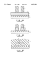
- FIGS. 4A to 4C are cross-sectional views showing a conventional interconnect line forming process.
- a well is formed in a semiconductor substrate 11, an element isolation area, not shown, is formed by an LOCOS method for instance, and a gate oxide film, gate electrode and source/drain structure are formed to provide a transistor.
- an insulating film 5 is deposited on the whole surface of a semiconductor substrate 11 and contact holes, not shown, are opened, a Ti film of, for example, 20 nm thick is deposited on the whole surface and a TiN film of, for example, 70 nm thick is formed on the Ti film.
- a barrier metal 4 is formed with the Ti film and TiN film.
- An Ag alloy film 3 of, for example, 600 nm thick is deposited on the barrier metal film 4 and a TiN film 2 of, for example, 30 nm thick is deposited on the Al alloy film 3.
- the TiN film 2 serves as an anti-reflective film.
- FIG. 4A shows a cross-sectional view showing a semiconductor device structure at that stage of manufacture.
- FIG. 4B is a cross-sectional view showing the semiconductor device at this stage of manufacture.
- a decomposition product of the resist film 1 is created, by slightly etching the resist film 1 by virtue of the RIE method, so that the product is deposited on the side wall of the Ag alloy film 2 being etched to provide a side wall protection film 6.
- the Al alloy film 3 is etched anisotropically.
- the decomposition product of the resist film 1 is not adequately supplied to the side wall of the Al alloy film.
- the Al alloy film 3 immediately below the anti-reflective film 2 is etched, to some extent, in a direction parallel to the substrate 11.
- the anti-reflective film 2 has a broader width than that of the immediately underlying Al alloy film 3 and extends, for example, about 50 nm, sideway relative to the Al alloy film 3, a state which will be referred to, hereinafter, as an "overhanging" state.
- FIG. 4C is a cross-sectional view showing a semiconductor device at this stage of manufacture.
- the decomposition product that is, the side wall protection film 6, of the resist film is removed to expose the overhanging type anti-reflective film 2.
- the insulating interlayer 7 formed by the CVD method faithfully reflects the shape of the interconnect line to be buried.
- the insulating interlayer 7 is grown, while reflecting the overhanging shape, so that a void 8 is created in the insulating interlayer 7 between adjacent interconnect lines.
- Such void 8 upon the planarization of the insulating interlayer 7, is exposed on the surface of the insulating interlayer 7.
- such void is groove-like and, if a second interconnect line is formed as it is, there is a possibility that there will occur a breakage in the second interconnect layer or a short-circuiting of the interconnect line due to the interconnect material entering in the groove.
- a multi-level interconnect structure is formed and a passivation film is deposited.
- the anti-reflective film being so overhung, creates voids, thus presenting a problem.
- a method for manufacturing a semiconductor device comprising the steps of:
- a semiconductor device comprising:
- interconnect line means having a lower surface and upper surface narrower in width than the lower surface in which an angle defined between the lower surface and a side surface joining an end of the lower surface and end of the upper surface is below 90°;
- an anti-reflective film provided on the interconnect line means and having a narrower width than that of the upper surface of the interconnect line means.
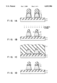
- FIGS. 1A to 1C are cross-sectional views showing a first embodiment of the present invention
- FIG. 1D is a cross-sectional view showing a modified example of the first embodiment.
- FIGS. 2A to 2D are cross-sectional views showing a second embodiment of the present invention.
- FIGS. 3A to 3D are cross-sectional views showing a third embodiment of the present invention.
- FIGS. 4A to 4C are cross-sectional views showing a conventional device.
- FIGS. 1A to 1C show a first embodiment of the present invention.
- the same reference numerals are employed to designate like parts or elements and any further explanation is, therefore, omitted for brevity's sake.
- a well is formed in a semiconductor substrate 11 and an element isolation area, not shown, is formed by a LOCOS method for example.
- a gate oxide film, gate electrode and a source/drain structure, not shown, are formed at an element area to provide a transistor not shown.
- an insulating film 5 is deposited on the whole surface of the substrate 11 and contact holes, not shown, are opened in the insulating film 5. Further, a Ti film of, for example, 20 nm thick, TiN film of, for example, 70 nm thick, Al alloy film 3 of, for example, 600 nm thick and TiN film of, for example, 30 nm thick are sequentially formed over the insulating film 5 and contact holes. The initially deposited Ti and TiN films serve as a barrier metal film 4. The finally deposited TiN film acts as an anti-reflective film 2.
- FIG. 1A a cross-sectional view showing a semiconductor device structure at this stage of manufacture.
- the semiconductor device structure is exposed with the plasma of the Cl 2 /BCl 3 gas.
- the Cl 2 /BCl 3 -mixed gas is used as a gas for working these films 2, 3 and 4 under the RIE process, but is so conditioned that it is quicker in the etching of the resist film than in that of the metal stacked layer structure as set out above.
- the condition comprises the use of a lower pressure than the working condition of the metal stacked layer structure, or the use of a lower partial pressure of the Cl 2 gas, or the use of a gas mixed with a He gas, etc.
- the resist film 1 is etched by ions in the plasma. The etching is started from the resist film above an end of the anti-reflective film 2. With the resist film 1 receded by the etching, the anti-reflective film 2 and side wall protection film 6 are exposed with the ions in the plasma. Since the anti-reflective film 2 is also etched under the above mentioned conditions, it is etched from its upper end side. The side wall protection film 6 is also etched. FIG.
- the anti-reflective film 2 ceases to overhang and the side surface of the metal layer stacked structure comprised of the anti-reflective film 2 and Al alloy film 3 creates a normal tapering structure. That is, the normal tapering structure is such that the Al alloy film 3 is narrower at its upper surface than at its lower surface and that an angle of a side surface, that is, a surface defined by connecting an end of its upper surface to an end of its lower surface, is below 90° and that the anti-reflective film 2 provided on the Al alloy film 3 is narrower in width than the Al alloy film 3.
- the side wall of the Al alloy film 3 is protected by the side wall protection film 6 formed of a decomposition product of the resist film and, since the etching proceeds downward from above, the Al alloy film 3 is etched sideway only to such an extent that the anti-reflective film 2 does not overhang. Under the above-mentioned etching conditions, the side wall protection film 6, together with the resist film 1, is normally etched.
- the underlying film (SiO 2 ) is also exposed with the Cl 2 /BCl 3 -mixed gas, since the etching rate of the SiO 2 under the gaseous plasma generation condition as set out above is as slow as 50 nm/min., no underlying film 5 is extremely etched even when it is exposed with the Cl 2 /BCl 3 gaseous plasma for a short time period.
- FIG. 1C is a cross-sectional view showing a semiconductor device structure at this stage of manufacture. Since the overhanging of the TiN film 2 is eliminated, any void resulting from such overhanging is not produced in the insulating interlayer 7.
- a multi-layered structure is formed on that semiconductor structure as required and a protective film is deposited thereon to complete a semiconductor device.
- a protective film is deposited thereon to complete a semiconductor device.
- the overhanging portion of the anti-reflective film is removed, by the plasma etching, after the formation of the interconnect lines, so that the side surface of the interconnect lines becomes a normal tapering shape.
- the resist film is fully left as it is after the formation of such interconnect lines and the overhanging portion of the TiN film is eliminated by subjection to the plasma
- the present invention is not restricted thereto.
- the resist film 1 may be isotropically etched by an O 2 ashing as shown in FIG. 1D or the interconnect lines may be exposed with the plasma after the resist film has been fully removed. Even in this case, it is possible to eliminate the overhanging portion of the TiN film and thus obtain the same effect as in the first embodiment.
- the RIE process is performed by using the plasma of the Cl 2 /BCl 3 gas. It is also possible to use the plasma of the Cl 2 /BCl 3 /Ar ga-and thus obtain the same effects as in the first embodiment.
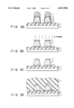
- FIGS. 2A to 2D show a second embodiment of the present invention.
- FIG. 2A is a cross-sectional view showing a semiconductor device structure at this stage of manufacture.
- the resist film 1 is subjected by an O 2 plasma to ashing and the resist film 1 and side wall protection film 6 are removed.
- FIG. 2B is a cross-sectional view showing a semiconductor device structure at this stage of manufacture.
- the overhanging portion of the TiN 2 is removed by this processing.
- the Ar has an atomic weight of 39 and is a relatively heavy gas and the sputtering effect by the Ar plasma is high.
- An overhanging portion in particular of the anti-reflective film 2, being directly exposed with the Ar plasma, is readily eliminated.
- the Ar being a rare gas, reveals a lower reactivity with a metal, such as an Al alloy film 3.
- FIG. 2C is a cross-sectional view showing a semiconductor device structure at this stage of manufacture.
- FIG. 2D is a cross-sectional view showing a semiconductor device at this time of manufacture.
- a multi-level interconnect line is provided and a passivation film is deposited on the multi-level interconnect line. Even in the formation of the multi-level interconnect line, it is needless to say that it is possible to use the etching method of the present invention.
- the side surface of the interconnect line becomes a normal tapering shape, so that it is possible to form an insulating interlayer free of any voids and hence to prevent any breakage and any short-circuiting to the interconnect lines formed over the insulating interlayer.
- the Ar plasma has been explained as being used so as to remove the overhanging portion of the anti-reflective film
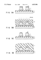
- FIGS. 3A to 3D show a third embodiment of the present invention.
- transistors, etc. are formed at a substrate 11, an insulating film 5 is deposited on the substrate 11 and contacts, not shown, are opened there. Then a barrier metal film 4 of Ti/TiN, Al alloy film 3 and anti-reflective film 2 of TiN are sequentially deposited over the insulating film 5.
- a resist film 1 of, for example, 1500 nm thick is coated on the anti-reflective film 2 and patterned by the photolithography technique.
- the metal layer stacked structure (metal films 2, 3, 4) is etched, by a Cl 2 /BCl 3 -mixed gas,with the resist film 1 used as a mask. By doing so, these metal films 2, 3 and 4 are worked to provide a normal tapering shape.
- FIG. 3A is a cross-sectional view showing a semiconductor device structure at this stage of manufacture.
- FIG. 3B is a cross-sectional view showing a semiconductor device structure at this stage of manufacture.
- the TiN film 2 is etched by the CDE step using a CF 4 /O 2 -mixed gas. In the CDE processing, etching proceeds in an isotropical fashion, so that the anti-reflective film 2 is removed around from its end. Since the resist film 10 is buried between the interconnect lines, the barrier metal film 4 containing the TiN film is not etched by the CDE processing.
- the Al alloy film 3 is not etched by a fluorine-based gas so that its configuration does not vary by the CDE process. In this way, the overhanging portion of the anti-reflective film 2 is eliminated by the CDE process.
- FIG. 3C is a cross-sectional view showing a semiconductor device structure at this stage of manufacture.
- the insulating interlayer 7 is deposited between the interconnect lines and over the interconnect lines to have them buried therewith. By doing so, a semiconductor device is completed. Even in the formation of the multi-level interconnect lines, it is needless to say that the etching method of the present invention can also be used.
- the overhanging portion of the anti-reflective film is removed and the side surface of the interconnect line becomes a normal taper shape.
Applications Claiming Priority (2)
| Application Number | Priority Date | Filing Date | Title |
|---|---|---|---|
| JP8138349A JPH09321053A (ja) | 1996-05-31 | 1996-05-31 | 半導体装置及びその製造方法 |
| JP8-138349 | 1996-05-31 |
Publications (1)
| Publication Number | Publication Date |
|---|---|
| US6033986A true US6033986A (en) | 2000-03-07 |
Family
ID=15219857
Family Applications (1)
| Application Number | Title | Priority Date | Filing Date |
|---|---|---|---|
| US08/820,531 Expired - Fee Related US6033986A (en) | 1996-05-31 | 1997-03-19 | Semiconductor device having an anti- reflective film on an interconnect line and a method for manufacturing the same |
Country Status (2)
| Country | Link |
|---|---|
| US (1) | US6033986A (ja) |
| JP (1) | JPH09321053A (ja) |
Cited By (6)
| Publication number | Priority date | Publication date | Assignee | Title |
|---|---|---|---|---|
| US6277745B1 (en) * | 1998-12-28 | 2001-08-21 | Taiwan Semiconductor Manufacturing Company | Passivation method of post copper dry etching |
| US6432812B1 (en) * | 2001-07-16 | 2002-08-13 | Lsi Logic Corporation | Method of coupling capacitance reduction |
| US20060057852A1 (en) * | 2003-09-25 | 2006-03-16 | Qiang Fu | Process for low k dielectric plasma etching with high selectivity to deep uv photoresist |
| KR20110099226A (ko) * | 2008-10-28 | 2011-09-07 | 에실러에떼르나쇼날(꽁빠니제네랄돕띠끄) | 코팅된 안과용 기재에 마킹하기 위한 방법 및 장치 |
| US20120038056A1 (en) * | 2010-08-10 | 2012-02-16 | International Business Machines Corporation | Interconnect structure for improved time dependent dielectric breakdown |
| US9064727B2 (en) * | 2012-11-07 | 2015-06-23 | International Business Machines Corporation | Sputter and surface modification etch processing for metal patterning in integrated circuits |
Families Citing this family (1)
| Publication number | Priority date | Publication date | Assignee | Title |
|---|---|---|---|---|
| KR100435785B1 (ko) * | 2001-12-22 | 2004-06-12 | 동부전자 주식회사 | 반도체 소자의 금속배선 형성방법 |
Citations (4)
| Publication number | Priority date | Publication date | Assignee | Title |
|---|---|---|---|---|
| US4919748A (en) * | 1989-06-30 | 1990-04-24 | At&T Bell Laboratories | Method for tapered etching |
| JPH02143425A (ja) * | 1988-11-24 | 1990-06-01 | Sony Corp | A1又はa1合金膜のテーパーエッチング方法 |
| US5174856A (en) * | 1991-08-26 | 1992-12-29 | Applied Materials, Inc. | Method for removal of photoresist over metal which also removes or inactivates corrosion-forming materials remaining from previous metal etch |
| US5277757A (en) * | 1991-03-18 | 1994-01-11 | Sony Corporation | Dry etching method |
-
1996
- 1996-05-31 JP JP8138349A patent/JPH09321053A/ja active Pending
-
1997
- 1997-03-19 US US08/820,531 patent/US6033986A/en not_active Expired - Fee Related
Patent Citations (4)
| Publication number | Priority date | Publication date | Assignee | Title |
|---|---|---|---|---|
| JPH02143425A (ja) * | 1988-11-24 | 1990-06-01 | Sony Corp | A1又はa1合金膜のテーパーエッチング方法 |
| US4919748A (en) * | 1989-06-30 | 1990-04-24 | At&T Bell Laboratories | Method for tapered etching |
| US5277757A (en) * | 1991-03-18 | 1994-01-11 | Sony Corporation | Dry etching method |
| US5174856A (en) * | 1991-08-26 | 1992-12-29 | Applied Materials, Inc. | Method for removal of photoresist over metal which also removes or inactivates corrosion-forming materials remaining from previous metal etch |
Cited By (8)
| Publication number | Priority date | Publication date | Assignee | Title |
|---|---|---|---|---|
| US6277745B1 (en) * | 1998-12-28 | 2001-08-21 | Taiwan Semiconductor Manufacturing Company | Passivation method of post copper dry etching |
| US6432812B1 (en) * | 2001-07-16 | 2002-08-13 | Lsi Logic Corporation | Method of coupling capacitance reduction |
| US20060057852A1 (en) * | 2003-09-25 | 2006-03-16 | Qiang Fu | Process for low k dielectric plasma etching with high selectivity to deep uv photoresist |
| KR20110099226A (ko) * | 2008-10-28 | 2011-09-07 | 에실러에떼르나쇼날(꽁빠니제네랄돕띠끄) | 코팅된 안과용 기재에 마킹하기 위한 방법 및 장치 |
| US20120038056A1 (en) * | 2010-08-10 | 2012-02-16 | International Business Machines Corporation | Interconnect structure for improved time dependent dielectric breakdown |
| US8431486B2 (en) * | 2010-08-10 | 2013-04-30 | International Business Machines Corporation | Interconnect structure for improved time dependent dielectric breakdown |
| US9064727B2 (en) * | 2012-11-07 | 2015-06-23 | International Business Machines Corporation | Sputter and surface modification etch processing for metal patterning in integrated circuits |
| US9263393B2 (en) | 2012-11-07 | 2016-02-16 | Globalfoundries Inc. | Sputter and surface modification etch processing for metal patterning in integrated circuits |
Also Published As
| Publication number | Publication date |
|---|---|
| JPH09321053A (ja) | 1997-12-12 |
Similar Documents
| Publication | Publication Date | Title |
|---|---|---|
| US7482279B2 (en) | Method for fabricating semiconductor device using ArF photolithography capable of protecting tapered profile of hard mask | |
| US6448176B1 (en) | Dual damascene processing for semiconductor chip interconnects | |
| US6140224A (en) | Method of forming a tungsten plug | |
| US20010014525A1 (en) | Process for forming trenches and contacts during the formation of a semiconductor memory device | |
| JPH06140396A (ja) | 半導体装置とその製法 | |
| US6114235A (en) | Multipurpose cap layer dielectric | |
| US6383862B2 (en) | Method of forming a contact hole in a semiconductor substrate using oxide spacers on the sidewalls of the contact hole | |
| US6489201B2 (en) | Method for manufacturing a semiconductor device | |
| US6495452B1 (en) | Method to reduce capacitance for copper interconnect structures | |
| US6033986A (en) | Semiconductor device having an anti- reflective film on an interconnect line and a method for manufacturing the same | |
| US6326296B1 (en) | Method of forming dual damascene structure with improved contact/via edge integrity | |
| US6017824A (en) | Passivation etching procedure, using a polysilicon stop layer, for repairing embedded DRAM cells | |
| US6245657B1 (en) | Self-aligned, low contact resistance, via fabrication process | |
| US6258709B1 (en) | Formation of electrical interconnect lines by selective metal etch | |
| US6313029B1 (en) | Method for forming multi-layer interconnection of a semiconductor device | |
| JP2001093888A (ja) | 半導体装置の製造方法 | |
| US6982219B2 (en) | Semiconductor device with fuse box and method for fabricating the same | |
| US20020072217A1 (en) | Method for improving contact reliability in semiconductor devices | |
| KR100438630B1 (ko) | 반도체 장치의 제조방법 | |
| US6815337B1 (en) | Method to improve borderless metal line process window for sub-micron designs | |
| US6287752B1 (en) | Semiconductor device, method of manufacturing a semiconductor device, and method of forming a pattern for semiconductor device | |
| US6881678B2 (en) | Method for forming a dual damascene structure in a semiconductor device | |
| JPH07221110A (ja) | 半導体装置の配線構造とその製造方法 | |
| KR100881082B1 (ko) | 듀얼 다마신 공정을 이용한 배선 형성 방법 | |
| JP2000208620A (ja) | 半導体装置の製造方法 |
Legal Events
| Date | Code | Title | Description |
|---|---|---|---|
| AS | Assignment |
Owner name: KABUSHIKI KAISHA TOSHIBA, JAPAN Free format text: ASSIGNMENT OF ASSIGNORS INTEREST;ASSIGNOR:ITOH, KATSUYA;REEL/FRAME:008455/0602 Effective date: 19970311 |
|
| FPAY | Fee payment |
Year of fee payment: 4 |
|
| FPAY | Fee payment |
Year of fee payment: 8 |
|
| REMI | Maintenance fee reminder mailed | ||
| LAPS | Lapse for failure to pay maintenance fees | ||
| STCH | Information on status: patent discontinuation |
Free format text: PATENT EXPIRED DUE TO NONPAYMENT OF MAINTENANCE FEES UNDER 37 CFR 1.362 |
|
| FP | Lapsed due to failure to pay maintenance fee |
Effective date: 20120307 |