US5959906A - Semiconductor memory device with a fully accessible redundant memory cell array - Google Patents
Semiconductor memory device with a fully accessible redundant memory cell array Download PDFInfo
- Publication number
- US5959906A US5959906A US08/977,844 US97784497A US5959906A US 5959906 A US5959906 A US 5959906A US 97784497 A US97784497 A US 97784497A US 5959906 A US5959906 A US 5959906A
- Authority
- US
- United States
- Prior art keywords
- bit
- row
- row address
- redundant
- memory cell
- Prior art date
- Legal status (The legal status is an assumption and is not a legal conclusion. Google has not performed a legal analysis and makes no representation as to the accuracy of the status listed.)
- Expired - Lifetime
Links
Images


Classifications
-
- G—PHYSICS
- G11—INFORMATION STORAGE
- G11C—STATIC STORES
- G11C11/00—Digital stores characterised by the use of particular electric or magnetic storage elements; Storage elements therefor
- G11C11/21—Digital stores characterised by the use of particular electric or magnetic storage elements; Storage elements therefor using electric elements
- G11C11/34—Digital stores characterised by the use of particular electric or magnetic storage elements; Storage elements therefor using electric elements using semiconductor devices
- G11C11/40—Digital stores characterised by the use of particular electric or magnetic storage elements; Storage elements therefor using electric elements using semiconductor devices using transistors
- G11C11/401—Digital stores characterised by the use of particular electric or magnetic storage elements; Storage elements therefor using electric elements using semiconductor devices using transistors forming cells needing refreshing or charge regeneration, i.e. dynamic cells
- G11C11/4063—Auxiliary circuits, e.g. for addressing, decoding, driving, writing, sensing or timing
- G11C11/407—Auxiliary circuits, e.g. for addressing, decoding, driving, writing, sensing or timing for memory cells of the field-effect type
-
- G—PHYSICS
- G11—INFORMATION STORAGE
- G11C—STATIC STORES
- G11C29/00—Checking stores for correct operation ; Subsequent repair; Testing stores during standby or offline operation
- G11C29/70—Masking faults in memories by using spares or by reconfiguring
- G11C29/78—Masking faults in memories by using spares or by reconfiguring using programmable devices
- G11C29/80—Masking faults in memories by using spares or by reconfiguring using programmable devices with improved layout
- G11C29/808—Masking faults in memories by using spares or by reconfiguring using programmable devices with improved layout using a flexible replacement scheme
-
- G—PHYSICS
- G11—INFORMATION STORAGE
- G11C—STATIC STORES
- G11C29/00—Checking stores for correct operation ; Subsequent repair; Testing stores during standby or offline operation
- G11C29/70—Masking faults in memories by using spares or by reconfiguring
- G11C29/78—Masking faults in memories by using spares or by reconfiguring using programmable devices
- G11C29/785—Masking faults in memories by using spares or by reconfiguring using programmable devices with redundancy programming schemes
Definitions
- the present invention relates to a semiconductor memory device and, more particularly, to a semiconductor memory device having a redundant memory cell array.
- FIG. 1 is a block diagram of a conventional semiconductor memory device having a redundant memory cell array 108.
- a row address buffer 101 latches an n-bit row address RA that is input to the semiconductor memory device by an external device when a row address strobe signal RASB, that is buffered by a row address strobe buffer 110, is strobed by the external device.
- the row address strobe buffer 110 is synchronized with a system clock to buffer the externally applied row address strobe signal RASB.
- a control signal generator 109 delays the buffered RASB signal output from the row address strobe buffer 110 by a predetermined period of time in order to generate a delayed row address strobe signal RASBD.
- a normal memory cell array 106 is composed of a plurality of memory cells arranged in a matrix pattern. Each memory cell can be accessed by the combination of a normal word line and a bit line. Where the row address RA is composed of n bits, the number of individually driven normal word lines included in the memory cell array 106 should be less than 2 n . Each one of the normal word lines included in the memory cell array 106 is selectively activated by a corresponding value of the row address RA.
- Row address decoding is performed in order to select one of the word lines of normal memory cell array 106.
- the row address decoding related to the normal memory cell array 106 is performed by a row predecoder 102 and a row decoder 105.
- the row predecoder 102 receives (n-k) bits of the n row address bits output by row address buffer 101 while the remaining k bits are passed through to row decoder 105.
- the row predecoder 102 decodes the (n-k) bits of the row address and outputs the result as predecoder row address signal PRA, which is composed of 2.sup.(n-k) signals.
- the signal PRA and the remaining k bits of row address RA are applied to the row decoder 105.
- the row decoder 105 includes 2.sup.(n-k) k-bit decoders which each decode the remaining k bits and control a corresponding one of 2.sup.(n-k) normal word line drivers.
- the 2.sup.(n-k) k-bit decoders are enabled by the PRA signal output by the row predecoder 102.
- the row address decoding function is performed by the row predecoder 102 along with the k-bit decoders included in row decoder 105.
- the normal word line drivers included in the row decoder 105 are enabled or disabled in response to the signal PRRE output by row decoder disable signal generator 103 and the control signal RASBD and, responsive to the decoded row address RA, drive one of the 2 n normal word lines of the normal memory cell array 106 which are coupled to the row decoder 106.
- the memory device of FIG. 1 also includes redundant memory cell array 108 which is used to replace defective memory cells which may occur in the normal memory cell array 106.
- Each memory cell included in the redundant memory cell array 108 is accessible through the combination of a redundant word line and a bit line.
- the size of the redundant memory cell array 108 is determined during design thereof based upon the probability that defects will be generated during the manufacturing process.
- a row address for driving each redundant word line is not determined during the design of the memory device but during a repair phase after the memory device has been fabricated.
- the row address decoding for the redundant memory cell array 108 is performed by a redundant row fuse decoder 104 and a redundant row decoder 107.
- the redundant row fuse decoder 104 receives m bits of the row address output from the row address buffer 101, while the remaining (n-m) bits of the row address RA are passed through to the redundant row decoder 107.
- the redundant row fuse decoder 104 is composed of a plurality of m-bit address fuse portions 121, 122 and 123.
- the ellipses in the drawing indicate that more m bit address fuse portions can be included in a particular circuit design.
- the m-bit address fuse portions 121, 122 and 123 each decode m bits of a row address corresponding to word line in the normal memory cell array 106 that contains a defective memory cell. For example, when the row address RA that specifies a normal word line in the normal memory cell array 106 is composed of 11 bits, the number of bits m decoded in each address fuse portion is 7.
- defective row addresses 10010111000
- the m-bit address fuse portion is coded using the lower 7 bits, i.e. 0111000.
- the coding of the defective row addresses is performed by selectively shorting the fuse array in one of the m bit address fuse circuits 121, 122 or 123 to decode the selected defective address.
- Groups which do not have a corresponding m bit address fuse portion 121, 122 or 123 cannot be repaired. For example, if the group in which the upper 4 bits of the row address is (1001) is not assigned an m bit address fuse portion, then defects occurring in the word lines of the normal memory cell array 106 in which the row address of the upper 4 bits is (1001) cannot be repaired.
- each m bit address fuse portion 121, 122 and 123 can only decode one word line in a group.
- the two defective memory cells can both be repaired.
- both the defective word lines cannot be replaced. For example, if a defective memory cell occurs in the word line with the row address (10010111000) and another defective memory cell occurs in the word line with the row address (10010100110), then only one of the defective cells can be replaced. In this scheme, defective memory cells can occur that may not be replaced even though a usable redundant memory cell in redundant memory cell array 108 exists.
- the outputs RED1, RED2, . . . , REDi of m-bit address fuse portions 121, 122 and 123 are activated responsive to an m bit defective row address of the row address signal RA that has been coded into the fuse portion.
- An (n-m)-bit decoder 130 included in the redundant row decoder 107 decodes the remaining higher order (n-m) bits of the row addresses RA and outputs a signal responsive to each group of (n-m) bits in the row address signal RA.
- Logic gates 141, 142 and 143 combine the output signals from the (n-m) bit decoder 130 with the output of each of the m-bit address fuse portions 121, 122 and 123.
- logic gate 141 combines the first output of the (n-m)-bit decoder 130 and the RED1 signal and generates an output signal when both inputs are active.
- logic gate 142 combines the second output of the (n-m)-bit decoder 130 and the RED2 signal.
- logic gate 143 combines the last output of the (n-m)-bit decoder 130 and the REDi signal.
- the logic gate 141 is activated when the upper 4-bits of the row address signal RA is (0000) and RED1 is active
- the logic gate 142 is activated when the upper 4-bits of the row address signal RA is (0001) and RED2 is active
- the logic gate 143 is activated when the upper 4-bits of the row address signal RA is (1111) and the REDi is active.
- Logic gates 151, 152 and 153 transmit the outputs of the logic gates 141, 142 and 143, respectively, to the corresponding redundant word line drivers 161, 162 and 163, respectively, when the delayed row address strobe signal RASBD is active.
- Redundant word line drivers 161, 162 and 163 output signals which drive the corresponding redundant word lines R-WL(1), R-WL(2), . . . , R-WL(I), respectively, when the corresponding output signal from one of logic gates 141, 142 or 143 is active.
- a column address strobe buffer 111 receives a column address strobe signal CASB in synchronization with the system clock.
- a column address buffer 113 latches an externally input column address signal CA when strobed by the column address strobe signal CASB.
- a column decoder 112 decodes the column address CA and generates a column line select signal which enables the column select line corresponding to the value of the column address signal CA.
- the row decoder disable signal generator 103 generates the row decoder disable signal PRRE which is activated when one of the outputs of the redundant row fuse decoder 104 is active.
- the row decoder 105 is disabled so that it does not perform a decoding operation when the row decoder disable signal PRRE is active.
- the conventional semiconductor memory device described above suffers from the problem that a defective memory cell in normal memory cell array 106 cannot be replaced even though a replacement cell in redundant memory cell array 108 is available because more than one row has a defective memory cell within the same group.
- the memory device above also runs into problems with slower operating speed and increased chip layout area require for the circuit design.
- a semiconductor memory device which includes a normal memory cell array including a plurality of memory cells organized into 2 n word lines and a plurality of column bit lines.
- the device also includes a normal row address decoder configured to activate one of the word lines of the normal memory cell array responsive to an externally input n-bit row address signal, wherein the normal row address decoder is further configured to be inhibited from activating one of the 2 n word lines of the normal memory cell array responsive to a normal row decoder disable signal.
- a redundant row fuse decoder which has a plurality of n-bit address fuse portions wherein each one of the plurality of n-bit address fuse portions is configured to be coded to respond to an n-bit defective row address in the externally input n-bit row address signal corresponding to one of the 2 n word lines of the normal memory cell array and generate an redundant word line activation signal, and wherein the redundant row fuse decoder is further configured to generate the normal row decoder disable signal responsive to the redundant word line activation signal.
- the device further includes a redundant memory cell array including a plurality of redundant rows of memory cells specified by a redundant word line and the plurality of column bit lines, wherein each one of the redundant rows of memory cells is configured to receive the redundant word line activation signal generated by one of the n-bit address fuse portion of the redundant row fuse decoder.
- An embodiment of a method according to the present invention for replacing defective memory cells in a normal memory cell array having 2 n rows includes providing a redundant memory cell array, specifying a predetermined n-bit defective row address by selectively blowing fuses in an n-bit redundant row address decoder, and decoding the predetermined n-bit defective row address from an externally input n-bit row address signal.
- the method also involves disabling the activation of the rows of the normal memory cell array responsive to decoding the predetermined n-bit defective row address from the externally input n-bit row address signal, and activating a row of the redundant memory cell array responsive to decoding the predetermined n-bit defective row address from the externally input n-bit row address signal
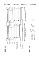
- FIG. 1 is a block diagram of a conventional semiconductor memory device.
- FIG. 2 is a block diagram of the redundant row fuse decoder and the redundant row decoder of FIG. 1.
- FIG. 3 is a block diagram of a semiconductor memory device according to the present invention.
- FIG. 4 is a detailed block diagram of the row decoder of FIG. 3.
- FIG. 5 is a circuit diagram of the normal word line control driving portion shown in FIG. 4.
- FIG. 6 is a block diagram of the redundant row fuse decoder shown in FIG. 3.
- FIG. 7 shows an embodiment of the n-bit address fuse portion shown in FIG. 6.
- FIG. 8 is a block diagram of the control driving portion shown in FIG. 3.
- FIG. 9 is a waveform diagram showing the internal signals of the conventional semiconductor memory device of FIG. 1.
- FIG. 10 is a waveform diagram showing the inner signals of the semiconductor memory device according to the present invention.
- FIG. 11 is a circuit diagram showing an embodiment of the row decoder disable signal generator shown in FIG. 3.
- FIG. 3 is a block diagram of an embodiment of a semiconductor memory device according to the present invention. Similar to the conventional memory device of FIG. 1, the memory device of the present invention includes a row address buffer 101, a row predecoder 102, a row decoder 105, a normal memory cell array 106, a redundant memory cell array 108, a control signal generator 109, a row address strobe buffer 110, a column address strobe buffer 111, a column address buffer 113 and a column decoder 112. The memory device of the present invention further includes a row decoder disable signal generator 310, a redundant row fuse decoder 320 and a control driving portion 330.
- the row address strobe buffer 110 synchronizes the externally input row address strobe signal RASB with the system clock by latching the signal RASB responsive to a system clock.
- the row address buffer 101 synchronizes the externally input n bit row address signal RA with the system clock by latching the row address signal RA responsive to the buffered RASB signal output from RASB buffer 110.
- the column address strobe buffer 111 synchronizes the externally input column address strobe signal CASB with the system clock by latching the CASB signal responsive to the system clock.
- the column address buffer 113 synchronizes the externally input column address CA with the system clock by latching the column address CA responsive to the buffered column address strobe signal CASB output from the CASB buffer 111.
- the column decoder 112 decodes and outputs the column address CA.
- An I/O port (not shown), that is also controlled by the decoded column address, is connected between the column lines of the normal memory cell array 106 and the redundant memory cell array 108, which also correspond to bit lines, and the input/output pins of the circuit.
- the normal memory cell array 106 is composed of a plurality of memory cells arranged in a matrix pattern. Each memory cell is accessed by the combination of the row address RA decoded by the row predecoder 102 and the row decoder 105 and the column or bit line address CA decoded by column decoder 112.
- FIG. 4 shows the row decoder 105 which includes a plurality of k-bit decoders 341, 342 and 343 and a plurality of normal word line control driving portions 351, 352 and 353.
- the k-bit decoders 341, 342 and 343 each perform the decoding function for the lower order k bits of the row address RA and are selectively enabled by a corresponding output signal PRA1, PRA2, . . . , PRAi from the row predecoder 102 which performs the decoding function on the upper (n-k) bits of the row address RA value in order to select one of the k-bit decoders 341, 342 and 343.
- DRAi are the outputs of k-bit decoders 341, 342 and 343, respectively, which transition to an active logic "low” level in response to the input of the corresponding row address RA value.
- the row decoder disable signal PRRE which is an active logic "high” level signal, is inverted by inverter 361 and input to NAND gate 371 which performs a NAND operation on the output of the inverter 361 and the control signal RASBD, which is an active logic "high” level signal.
- NOR gate 381 performs a NOR operation on the output signal DRA1 of the corresponding k-bit decoder and the output of the NAND gate 371 such that the output of the NOR gate 381 becomes active when the DRA1 signal is active, the control signal RASBD is active, and the row decoder disable signal PRRE is not active.
- the normal word line driver 391 activates the normal word line to which it is coupled when the output of NOR gate 381 is active.
- the redundant memory cell array 108 includes a plurality of redundant memory cells arranged in a matrix pattern.
- a redundant memory cell can be accessed by the combination of a redundant word line and a column, or bit, line.
- the redundant address for accessing the plurality of redundant word lines is not determined in the design step, but is specified in a repair step during manufacturing. Namely, the redundant memory cell array 108 is used to replace a defective memory cell in the normal memory cell array 106.
- the defective row address is assigned such that a redundant word line is activated by a defective row address.
- the n-bit address fuse portions 441, 442 and 443 included in the redundant row fuse decoder 330 activate the signals RED1, RED2, . . . , REDi, respectively, when the delayed row address strobe signal RASBD is active and the value of the row address RA stored and output by row address buffer 101 coincides with a defective row address assigned to one of the n-bit address fuse portions.
- Each n-bit address fuse portion includes a plurality of fuses 411, 412, 413, 414, . . . , 415, 416 which are coded for a particular defective row address by being selectively shorted.
- the bit values RA1-RAn and inverted bit values RA1B-RAnB of the row address are applied to the gates of NMOS transistors 421, 422, 423, 424, . . . , 425, 426 in order to decode the defective row address determined by the pattern in which the fuses 411-416 are selectively blown.
- the row decoder disable signal PRRE will disable the row decoder 105 in order to prevent it from decoding the row address RA and activating the corresponding normal word line in the normal memory cell array 106. Instead, the row address RA is decoded by the redundant row fuse decoder and a word line in the redundant memory cell array 108 is activated. Therefore, the read/write operation for the particular row address RA value is performed in the redundant memory cell array 108 instead of the normal memory cell array 106.
- FIG. 8 is a block diagram of the control driving portion 330 shown in FIG. 3 which includes a plurality of redundant word line driving portions 451, 452, . . . , 453.
- the redundant word line driving portions 451, 452, . . . , 453 activate the corresponding redundant word line R-W/L in the redundant memory cell array 108 when one of the output signals RED1, RED2, . . . , REDi of a corresponding redundant row fuse decoder is active.
- the precharge control signal PDPX is delayed for a predetermined amount of time before becoming active at a logic "high” level responsive to RASB becoming active, as indicated by the arrow from the falling edge of RASB to the rising edge of PDPX.
- one of the output signals PRA1-PRAi from the row predecoder 102 becomes active at a logic "low” level, in response to the value of the row address signal RA, and selects one of the k-bit decoders 342-343 in row decoder 105.
- the row decoder disable signal PRRE remains inactive at a logic "low” level because the value of RA corresponds to a word line in the normal memory cell array 106.
- the control signal RASBD becomes active at a logic "high” level after a predetermined amount of time elapses after the falling edge of the row address strobe signal RASB.
- the output of the selected k-bit decoder 342-343 of row decoder 105 becomes active at a "high” level and activates the normal word line corresponding thereto. Since the output of the redundant row decoder 107 remains inactive at a "low” level, the redundant word lines remain inactive in a "low” level state.
- FIG. 9 also illustrates the case in which a redundant word line is selected where the value of the row address RA input to the memory device corresponds to a defective row address.
- the row address strobe signal RASB drops to an active "low” level
- the precharge control signal PDPX rises to an active "high” level
- the delayed RASB signal RASBD rises to an active "high” level.
- the output signal PRA1-PRAi from the row predecoder 102 corresponding to the value of the RA signal also drops to an active "low” level.
- the row decoder disable signal PRRE will rise to an active "high” level responsive to an active output signal from redundant row fuse decoder 104 to disable row decoder 105 such that the normal row word lines output from row decoder 105 remain at an inactive "low” level.
- a redundant word line output from the redundant row decoder 107 will rise to an active "high” level to activate a redundant word line.
- FIG. 10 shows the waveforms for the internal signals of the semiconductor memory device according to the present invention for both the case in which the normal word line is selected and the case where a redundant word line is selected.
- the selected output PRA1-PRAi of the row decoder 105 rises to an "high” level in order to activate the corresponding normal word line to an active "high” level.
- all the output signals RED1-REDi of the redundant row fuse decoder 320 are in a "low” level non-active state. As a result, none of the redundant word lines are activated.
- a redundant word line is selected.
- the row address strobe signal RASB drops to an active "low” level
- the precharge control signal PDPX rises to an active "high” level
- the delayed RASB signal RASBD rises to an active "high” level after a predetermined delay.
- One of the outputs PRA1-PRAi from the row predecoder 102 will drop to an active "low” level.
- the row decoder disable signal PRRE will rise to an active "high” level in response to an active output signal RED1-REDi from the redundant row fuse decoder 320 which disable row decoder 105 causing the outputs of the row decoder 105 to remain at an inactive "low” level.
- the active output signal RED1-REDi from the redundant row fuse decoder 320 will activate the control driving portion 330 to drive the corresponding redundant word line.
- the above-mentioned semiconductor memory device can be implemented with a simple circuit structure. Thus, it is possible to increase the operating speed and reduce the required layout area for the memory device.
Landscapes
- Engineering & Computer Science (AREA)
- Microelectronics & Electronic Packaging (AREA)
- Computer Hardware Design (AREA)
- For Increasing The Reliability Of Semiconductor Memories (AREA)
- Dram (AREA)
Applications Claiming Priority (2)
| Application Number | Priority Date | Filing Date | Title |
|---|---|---|---|
| KR96-62130 | 1996-12-05 | ||
| KR1019960062130A KR100230393B1 (ko) | 1996-12-05 | 1996-12-05 | 반도체 메모리장치 |
Publications (1)
| Publication Number | Publication Date |
|---|---|
| US5959906A true US5959906A (en) | 1999-09-28 |
Family
ID=19486007
Family Applications (1)
| Application Number | Title | Priority Date | Filing Date |
|---|---|---|---|
| US08/977,844 Expired - Lifetime US5959906A (en) | 1996-12-05 | 1997-11-25 | Semiconductor memory device with a fully accessible redundant memory cell array |
Country Status (4)
| Country | Link |
|---|---|
| US (1) | US5959906A (ja) |
| JP (1) | JPH10172295A (ja) |
| KR (1) | KR100230393B1 (ja) |
| TW (1) | TW340219B (ja) |
Cited By (13)
| Publication number | Priority date | Publication date | Assignee | Title |
|---|---|---|---|---|
| US6243320B1 (en) * | 1998-07-29 | 2001-06-05 | Mitsubishi Denki Kabushiki Kaisha | Synchronous semiconductor memory device capable of selecting column at high speed |
| US6269034B1 (en) * | 1999-06-14 | 2001-07-31 | Nec Corporation | Semiconductor memory having a redundancy judgment circuit |
| US6272057B1 (en) * | 1999-04-07 | 2001-08-07 | Nec Corporation | Semiconductor memory device |
| US6356503B1 (en) * | 2000-02-23 | 2002-03-12 | Virage Logic Corp. | Reduced latency row selection circuit and method |
| US6484277B1 (en) * | 1999-05-19 | 2002-11-19 | Infineon Technologies Ag | Integrated memory having a redundancy function |
| US6731550B2 (en) * | 2002-05-31 | 2004-05-04 | Stmicroelectronics, Inc. | Redundancy circuit and method for semiconductor memory devices |
| US20040095836A1 (en) * | 2002-11-18 | 2004-05-20 | Samsung Electronics Co., Ltd. | Semiconductor memory device and layout method of the same |
| US20070247897A1 (en) * | 2006-04-21 | 2007-10-25 | Honeywell International Inc. | Partitioned random access and read only memory |
| US20070268761A1 (en) * | 2006-05-19 | 2007-11-22 | Anant Pratap Singh | Integrated circuit having memory array including row redundancy, and method of programming, controlling and/or operating same |
| US20080225613A1 (en) * | 2005-08-16 | 2008-09-18 | Morteza Cyrus Afghahi | Memory row and column redundancy |
| US20080252361A1 (en) * | 2005-03-07 | 2008-10-16 | Taiwan Semiconductor Manufacturing Co., Ltd. | Electrical fuses with redundancy |
| US9697878B2 (en) | 2011-05-20 | 2017-07-04 | Semiconductor Energy Laboratory Co., Ltd. | Word line divider and storage device |
| US20180075889A1 (en) * | 2012-04-10 | 2018-03-15 | Samsung Electronics Co., Ltd. | Memory system for access concentration decrease management and access concentration decrease method |
Families Citing this family (1)
| Publication number | Priority date | Publication date | Assignee | Title |
|---|---|---|---|---|
| KR100549942B1 (ko) * | 1999-08-19 | 2006-02-07 | 삼성전자주식회사 | 전력소모를 최소화한 늦은 라이트 타입 반도체 메모리 장치 |
Citations (3)
| Publication number | Priority date | Publication date | Assignee | Title |
|---|---|---|---|---|
| US5386386A (en) * | 1990-03-22 | 1995-01-31 | Kabushiki Kaisha Toshiba | Redundancy circuit having a spare memory block replacing defective memory cells in different blocks |
| US5708619A (en) * | 1992-07-14 | 1998-01-13 | Mosaid Technologies Incorporated | Column redundancy scheme for DRAM using normal and redundant column decoders programmed with defective array address and defective column address |
| US5768198A (en) * | 1996-07-15 | 1998-06-16 | Nec Corporation | Semiconductor memory having redundancy function in block write operation |
-
1996
- 1996-12-05 KR KR1019960062130A patent/KR100230393B1/ko not_active IP Right Cessation
-
1997
- 1997-08-23 TW TW086112129A patent/TW340219B/zh not_active IP Right Cessation
- 1997-10-30 JP JP9299134A patent/JPH10172295A/ja active Pending
- 1997-11-25 US US08/977,844 patent/US5959906A/en not_active Expired - Lifetime
Patent Citations (3)
| Publication number | Priority date | Publication date | Assignee | Title |
|---|---|---|---|---|
| US5386386A (en) * | 1990-03-22 | 1995-01-31 | Kabushiki Kaisha Toshiba | Redundancy circuit having a spare memory block replacing defective memory cells in different blocks |
| US5708619A (en) * | 1992-07-14 | 1998-01-13 | Mosaid Technologies Incorporated | Column redundancy scheme for DRAM using normal and redundant column decoders programmed with defective array address and defective column address |
| US5768198A (en) * | 1996-07-15 | 1998-06-16 | Nec Corporation | Semiconductor memory having redundancy function in block write operation |
Cited By (25)
| Publication number | Priority date | Publication date | Assignee | Title |
|---|---|---|---|---|
| US6333892B2 (en) | 1998-07-29 | 2001-12-25 | Mitsubishi Denki Kabushiki Kaisha | Synchronous semiconductor memory device capable of selecting column at high speed |
| US6243320B1 (en) * | 1998-07-29 | 2001-06-05 | Mitsubishi Denki Kabushiki Kaisha | Synchronous semiconductor memory device capable of selecting column at high speed |
| US6272057B1 (en) * | 1999-04-07 | 2001-08-07 | Nec Corporation | Semiconductor memory device |
| US6414887B2 (en) | 1999-04-07 | 2002-07-02 | Nec Corporation | Semiconductor memory device |
| US6484277B1 (en) * | 1999-05-19 | 2002-11-19 | Infineon Technologies Ag | Integrated memory having a redundancy function |
| US6269034B1 (en) * | 1999-06-14 | 2001-07-31 | Nec Corporation | Semiconductor memory having a redundancy judgment circuit |
| US6356503B1 (en) * | 2000-02-23 | 2002-03-12 | Virage Logic Corp. | Reduced latency row selection circuit and method |
| US6731550B2 (en) * | 2002-05-31 | 2004-05-04 | Stmicroelectronics, Inc. | Redundancy circuit and method for semiconductor memory devices |
| US20040095836A1 (en) * | 2002-11-18 | 2004-05-20 | Samsung Electronics Co., Ltd. | Semiconductor memory device and layout method of the same |
| US6765845B2 (en) * | 2002-11-18 | 2004-07-20 | Samsung Electronics Co., Ltd. | Hierarchical word line scheme with decoded block selecting signals and layout method of the same |
| US20080252361A1 (en) * | 2005-03-07 | 2008-10-16 | Taiwan Semiconductor Manufacturing Co., Ltd. | Electrical fuses with redundancy |
| US7724601B2 (en) * | 2005-03-07 | 2010-05-25 | Taiwan Semiconductor Manufacturing Co., Ltd. | Electrical fuses with redundancy |
| US7738308B2 (en) * | 2005-08-16 | 2010-06-15 | Novelies, Llc | Memory row and column redundancy |
| US20080225613A1 (en) * | 2005-08-16 | 2008-09-18 | Morteza Cyrus Afghahi | Memory row and column redundancy |
| US20070247897A1 (en) * | 2006-04-21 | 2007-10-25 | Honeywell International Inc. | Partitioned random access and read only memory |
| US7746686B2 (en) * | 2006-04-21 | 2010-06-29 | Honeywell International Inc. | Partitioned random access and read only memory |
| WO2007136812A3 (en) * | 2006-05-19 | 2008-07-17 | Innovative Silicon Sa | Memory array having row redundancy and method |
| WO2007136812A2 (en) * | 2006-05-19 | 2007-11-29 | Innovative Silicon S.A. | Memory array having row redundancy and method |
| US7499352B2 (en) * | 2006-05-19 | 2009-03-03 | Innovative Silicon Isi Sa | Integrated circuit having memory array including row redundancy, and method of programming, controlling and/or operating same |
| US20070268761A1 (en) * | 2006-05-19 | 2007-11-22 | Anant Pratap Singh | Integrated circuit having memory array including row redundancy, and method of programming, controlling and/or operating same |
| US9697878B2 (en) | 2011-05-20 | 2017-07-04 | Semiconductor Energy Laboratory Co., Ltd. | Word line divider and storage device |
| US20180075889A1 (en) * | 2012-04-10 | 2018-03-15 | Samsung Electronics Co., Ltd. | Memory system for access concentration decrease management and access concentration decrease method |
| US10529395B2 (en) * | 2012-04-10 | 2020-01-07 | Samsung Electronics Co., Ltd. | Memory system for access concentration decrease management and access concentration decrease method |
| US11024352B2 (en) | 2012-04-10 | 2021-06-01 | Samsung Electronics Co., Ltd. | Memory system for access concentration decrease management and access concentration decrease method |
| US11817174B2 (en) | 2012-04-10 | 2023-11-14 | Samsung Electronics Co., Ltd. | Memory system for access concentration decrease management and access concentration decrease method |
Also Published As
| Publication number | Publication date |
|---|---|
| KR19980044104A (ko) | 1998-09-05 |
| JPH10172295A (ja) | 1998-06-26 |
| TW340219B (en) | 1998-09-11 |
| KR100230393B1 (ko) | 1999-11-15 |
Similar Documents
| Publication | Publication Date | Title |
|---|---|---|
| US5422850A (en) | Semiconductor memory device and defective memory cell repair circuit | |
| US7035152B1 (en) | System and method for redundancy memory decoding | |
| US6275426B1 (en) | Row redundancy for content addressable memory | |
| US5576633A (en) | Block specific spare circuit | |
| EP0809186B1 (en) | Method and apparatus of redundancy for non-volatile memory integrated circuits | |
| US5959906A (en) | Semiconductor memory device with a fully accessible redundant memory cell array | |
| JPH06203592A (ja) | 改良型冗長センスアンプ制御を有する半導体メモリ | |
| US4791615A (en) | Memory with redundancy and predecoded signals | |
| US7688655B2 (en) | Semiconductor memory device and test method therefor | |
| US7379357B2 (en) | Semiconductor memory device having advanced repair circuit | |
| US6205515B1 (en) | Column redundancy circuitry with reduced time delay | |
| JP2000260199A (ja) | 半導体記憶装置 | |
| US20240274720A1 (en) | Concurrent compensation in a memory system | |
| US6414887B2 (en) | Semiconductor memory device | |
| CN115497543A (zh) | 存储器系统中的四分之一匹配并行补偿 | |
| US5870341A (en) | Memory column redundancy circuit | |
| JP3224317B2 (ja) | 冗長アドレスデコーダ | |
| JPH1116342A (ja) | 品種切り替え可能な半導体装置及びその動作試験方法 | |
| US6339554B1 (en) | Semiconductor memory device with replacement programming circuit | |
| US6304498B1 (en) | Semiconductor memory device capable of suppressing degradation in operation speed after replacement with redundant memory cell | |
| US5359563A (en) | Memory system with adaptable redundancy | |
| US20010026481A1 (en) | Method and apparatus for repairing defective columns of memory cells | |
| US20040208067A1 (en) | Row redundancy circuit | |
| JP4125448B2 (ja) | 半導体メモリ装置 | |
| US6249466B1 (en) | Row redundancy scheme |
Legal Events
| Date | Code | Title | Description |
|---|---|---|---|
| AS | Assignment |
Owner name: SAMSUNG ELECTRONICS CO.,LTD., KOREA, REPUBLIC OF Free format text: ASSIGNMENT OF ASSIGNORS INTEREST;ASSIGNORS:SONG, HO-SUNG;CHOI, JONG-HYUN;REEL/FRAME:008846/0514 Effective date: 19971107 |
|
| STCF | Information on status: patent grant |
Free format text: PATENTED CASE |
|
| FEPP | Fee payment procedure |
Free format text: PAYOR NUMBER ASSIGNED (ORIGINAL EVENT CODE: ASPN); ENTITY STATUS OF PATENT OWNER: LARGE ENTITY |
|
| FPAY | Fee payment |
Year of fee payment: 4 |
|
| FPAY | Fee payment |
Year of fee payment: 8 |
|
| FPAY | Fee payment |
Year of fee payment: 12 |