US5684368A - Smart driver for an array of LEDs - Google Patents
Smart driver for an array of LEDs Download PDFInfo
- Publication number
- US5684368A US5684368A US08/660,827 US66082796A US5684368A US 5684368 A US5684368 A US 5684368A US 66082796 A US66082796 A US 66082796A US 5684368 A US5684368 A US 5684368A
- Authority
- US
- United States
- Prior art keywords
- light emitting
- driver
- power
- array
- unique
- Prior art date
- Legal status (The legal status is an assumption and is not a legal conclusion. Google has not performed a legal analysis and makes no representation as to the accuracy of the status listed.)
- Expired - Lifetime
Links
- 230000004044 response Effects 0.000 claims abstract description 5
- 230000008878 coupling Effects 0.000 claims abstract 3
- 238000010168 coupling process Methods 0.000 claims abstract 3
- 238000005859 coupling reaction Methods 0.000 claims abstract 3
- 239000000758 substrate Substances 0.000 claims description 9
- 239000012780 transparent material Substances 0.000 claims description 5
- 238000000034 method Methods 0.000 claims description 3
- 239000010410 layer Substances 0.000 description 31
- 239000004020 conductor Substances 0.000 description 23
- 238000003491 array Methods 0.000 description 11
- 239000000463 material Substances 0.000 description 10
- 229910052751 metal Inorganic materials 0.000 description 6
- 239000002184 metal Substances 0.000 description 6
- 238000010586 diagram Methods 0.000 description 5
- 230000006870 function Effects 0.000 description 5
- 239000012044 organic layer Substances 0.000 description 5
- 229920000767 polyaniline Polymers 0.000 description 4
- 230000001276 controlling effect Effects 0.000 description 3
- AMGQUBHHOARCQH-UHFFFAOYSA-N indium;oxotin Chemical compound [In].[Sn]=O AMGQUBHHOARCQH-UHFFFAOYSA-N 0.000 description 3
- 239000011777 magnesium Substances 0.000 description 3
- 238000004519 manufacturing process Methods 0.000 description 3
- 229920000642 polymer Polymers 0.000 description 3
- 239000004065 semiconductor Substances 0.000 description 3
- 239000002356 single layer Substances 0.000 description 3
- 229920000265 Polyparaphenylene Polymers 0.000 description 2
- 229910052791 calcium Inorganic materials 0.000 description 2
- 239000011575 calcium Substances 0.000 description 2
- 230000008859 change Effects 0.000 description 2
- 239000003086 colorant Substances 0.000 description 2
- 230000007547 defect Effects 0.000 description 2
- ZUOUZKKEUPVFJK-UHFFFAOYSA-N diphenyl Chemical compound C1=CC=CC=C1C1=CC=CC=C1 ZUOUZKKEUPVFJK-UHFFFAOYSA-N 0.000 description 2
- 230000005525 hole transport Effects 0.000 description 2
- 229910052749 magnesium Inorganic materials 0.000 description 2
- 150000002739 metals Chemical class 0.000 description 2
- 238000012986 modification Methods 0.000 description 2
- 230000004048 modification Effects 0.000 description 2
- 150000002894 organic compounds Chemical class 0.000 description 2
- -1 poly(p-phenylenevinylene) Polymers 0.000 description 2
- 229920000553 poly(phenylenevinylene) Polymers 0.000 description 2
- 230000001105 regulatory effect Effects 0.000 description 2
- PXMXBAVBERHHTA-UHFFFAOYSA-N 2-(4-tert-butylphenyl)-5-(2-phenylphenyl)-1,3,4-oxadiazole Chemical compound C1=CC(C(C)(C)C)=CC=C1C1=NN=C(C=2C(=CC=CC=2)C=2C=CC=CC=2)O1 PXMXBAVBERHHTA-UHFFFAOYSA-N 0.000 description 1
- OYPRJOBELJOOCE-UHFFFAOYSA-N Calcium Chemical compound [Ca] OYPRJOBELJOOCE-UHFFFAOYSA-N 0.000 description 1
- XDTMQSROBMDMFD-UHFFFAOYSA-N Cyclohexane Chemical compound C1CCCCC1 XDTMQSROBMDMFD-UHFFFAOYSA-N 0.000 description 1
- WHXSMMKQMYFTQS-UHFFFAOYSA-N Lithium Chemical compound [Li] WHXSMMKQMYFTQS-UHFFFAOYSA-N 0.000 description 1
- FYYHWMGAXLPEAU-UHFFFAOYSA-N Magnesium Chemical compound [Mg] FYYHWMGAXLPEAU-UHFFFAOYSA-N 0.000 description 1
- 230000032683 aging Effects 0.000 description 1
- 229920000109 alkoxy-substituted poly(p-phenylene vinylene) Polymers 0.000 description 1
- 229910052782 aluminium Inorganic materials 0.000 description 1
- XAGFODPZIPBFFR-UHFFFAOYSA-N aluminium Chemical compound [Al] XAGFODPZIPBFFR-UHFFFAOYSA-N 0.000 description 1
- 235000010290 biphenyl Nutrition 0.000 description 1
- 239000004305 biphenyl Substances 0.000 description 1
- 230000000903 blocking effect Effects 0.000 description 1
- XZCJVWCMJYNSQO-UHFFFAOYSA-N butyl pbd Chemical compound C1=CC(C(C)(C)C)=CC=C1C1=NN=C(C=2C=CC(=CC=2)C=2C=CC=CC=2)O1 XZCJVWCMJYNSQO-UHFFFAOYSA-N 0.000 description 1
- 229910052792 caesium Inorganic materials 0.000 description 1
- TVFDJXOCXUVLDH-UHFFFAOYSA-N caesium atom Chemical compound [Cs] TVFDJXOCXUVLDH-UHFFFAOYSA-N 0.000 description 1
- VBVAVBCYMYWNOU-UHFFFAOYSA-N coumarin 6 Chemical group C1=CC=C2SC(C3=CC4=CC=C(C=C4OC3=O)N(CC)CC)=NC2=C1 VBVAVBCYMYWNOU-UHFFFAOYSA-N 0.000 description 1
- 230000001351 cycling effect Effects 0.000 description 1
- 230000008021 deposition Effects 0.000 description 1
- 239000002019 doping agent Substances 0.000 description 1
- 239000007850 fluorescent dye Substances 0.000 description 1
- 239000011521 glass Substances 0.000 description 1
- 238000010348 incorporation Methods 0.000 description 1
- 229910052738 indium Inorganic materials 0.000 description 1
- 229910052744 lithium Inorganic materials 0.000 description 1
- 239000011368 organic material Substances 0.000 description 1
- 239000002245 particle Substances 0.000 description 1
- 229920002120 photoresistant polymer Polymers 0.000 description 1
- 125000002924 primary amino group Chemical group [H]N([H])* 0.000 description 1
- 239000010453 quartz Substances 0.000 description 1
- 238000005215 recombination Methods 0.000 description 1
- 230000006798 recombination Effects 0.000 description 1
- VYPSYNLAJGMNEJ-UHFFFAOYSA-N silicon dioxide Inorganic materials O=[Si]=O VYPSYNLAJGMNEJ-UHFFFAOYSA-N 0.000 description 1
Images


Classifications
-
- G—PHYSICS
- G09—EDUCATION; CRYPTOGRAPHY; DISPLAY; ADVERTISING; SEALS
- G09G—ARRANGEMENTS OR CIRCUITS FOR CONTROL OF INDICATING DEVICES USING STATIC MEANS TO PRESENT VARIABLE INFORMATION
- G09G3/00—Control arrangements or circuits, of interest only in connection with visual indicators other than cathode-ray tubes
- G09G3/20—Control arrangements or circuits, of interest only in connection with visual indicators other than cathode-ray tubes for presentation of an assembly of a number of characters, e.g. a page, by composing the assembly by combination of individual elements arranged in a matrix no fixed position being assigned to or needed to be assigned to the individual characters or partial characters
- G09G3/22—Control arrangements or circuits, of interest only in connection with visual indicators other than cathode-ray tubes for presentation of an assembly of a number of characters, e.g. a page, by composing the assembly by combination of individual elements arranged in a matrix no fixed position being assigned to or needed to be assigned to the individual characters or partial characters using controlled light sources
- G09G3/30—Control arrangements or circuits, of interest only in connection with visual indicators other than cathode-ray tubes for presentation of an assembly of a number of characters, e.g. a page, by composing the assembly by combination of individual elements arranged in a matrix no fixed position being assigned to or needed to be assigned to the individual characters or partial characters using controlled light sources using electroluminescent panels
- G09G3/32—Control arrangements or circuits, of interest only in connection with visual indicators other than cathode-ray tubes for presentation of an assembly of a number of characters, e.g. a page, by composing the assembly by combination of individual elements arranged in a matrix no fixed position being assigned to or needed to be assigned to the individual characters or partial characters using controlled light sources using electroluminescent panels semiconductive, e.g. using light-emitting diodes [LED]
- G09G3/3208—Control arrangements or circuits, of interest only in connection with visual indicators other than cathode-ray tubes for presentation of an assembly of a number of characters, e.g. a page, by composing the assembly by combination of individual elements arranged in a matrix no fixed position being assigned to or needed to be assigned to the individual characters or partial characters using controlled light sources using electroluminescent panels semiconductive, e.g. using light-emitting diodes [LED] organic, e.g. using organic light-emitting diodes [OLED]
- G09G3/3216—Control arrangements or circuits, of interest only in connection with visual indicators other than cathode-ray tubes for presentation of an assembly of a number of characters, e.g. a page, by composing the assembly by combination of individual elements arranged in a matrix no fixed position being assigned to or needed to be assigned to the individual characters or partial characters using controlled light sources using electroluminescent panels semiconductive, e.g. using light-emitting diodes [LED] organic, e.g. using organic light-emitting diodes [OLED] using a passive matrix
-
- G—PHYSICS
- G09—EDUCATION; CRYPTOGRAPHY; DISPLAY; ADVERTISING; SEALS
- G09G—ARRANGEMENTS OR CIRCUITS FOR CONTROL OF INDICATING DEVICES USING STATIC MEANS TO PRESENT VARIABLE INFORMATION
- G09G2320/00—Control of display operating conditions
- G09G2320/02—Improving the quality of display appearance
- G09G2320/0223—Compensation for problems related to R-C delay and attenuation in electrodes of matrix panels, e.g. in gate electrodes or on-substrate video signal electrodes
-
- G—PHYSICS
- G09—EDUCATION; CRYPTOGRAPHY; DISPLAY; ADVERTISING; SEALS
- G09G—ARRANGEMENTS OR CIRCUITS FOR CONTROL OF INDICATING DEVICES USING STATIC MEANS TO PRESENT VARIABLE INFORMATION
- G09G2320/00—Control of display operating conditions
- G09G2320/04—Maintaining the quality of display appearance
- G09G2320/043—Preventing or counteracting the effects of ageing
-
- G—PHYSICS
- G09—EDUCATION; CRYPTOGRAPHY; DISPLAY; ADVERTISING; SEALS
- G09G—ARRANGEMENTS OR CIRCUITS FOR CONTROL OF INDICATING DEVICES USING STATIC MEANS TO PRESENT VARIABLE INFORMATION
- G09G3/00—Control arrangements or circuits, of interest only in connection with visual indicators other than cathode-ray tubes
- G09G3/20—Control arrangements or circuits, of interest only in connection with visual indicators other than cathode-ray tubes for presentation of an assembly of a number of characters, e.g. a page, by composing the assembly by combination of individual elements arranged in a matrix no fixed position being assigned to or needed to be assigned to the individual characters or partial characters
- G09G3/2007—Display of intermediate tones
- G09G3/2014—Display of intermediate tones by modulation of the duration of a single pulse during which the logic level remains constant
Definitions
- the present invention pertains to arrays of light emitting devices and more specifically to apparatus for addressing and driving the arrays.
- Arrays of light emitting devices are becoming very popular as displays in portable electronic devices and the like. Arrays of organic light emitting devices are especially desirable because of the ease of fabrication. Also, organic light emitting devices are relatively bright, all, or most, of the colors desired are relatively easy to achieve, and the cost of fabrication and operation are relatively low.
- the electrically conductive terminal is formed of organic or inorganic conductors, such as conductive polyaniline (PANI) or indium-tin-oxide (ITO), which are substantially transparent to visible light so that the emitted light exits through the substrate.
- PANI conductive polyaniline
- ITO indium-tin-oxide
- the transparent electrically conductive material from which the contact is formed i.e. indium-tin-oxide (ITO) or the like, has a relatively high resistance so that forming it into row or column conductors in the array substantially increases the resistance between column drivers, an addressed light emitting device, and a row driver.
- ITO indium-tin-oxide
- the light emitting device at the first row crossing has a resistance between it and the column driver of one unit.
- the light emitting device at the second row crossing has a resistance between it and the column driver of two units.
- the light emitting device at the n th row crossing has a resistance between it and the column driver of n units.
- the voltage dropped across each separate light emitting device in a column changes.
- aging, use, etc. have a tendency to change the amount of current (or applied voltage) required to maintain a uniform brightness.
- a smart driver in combination with a light emitting device having first and second terminals and an associated resistance.
- a column driver is coupled to the first terminal of the light emitting device and a row driver is coupled to the second terminal of the light emitting device to form an addressed circuit including the associated resistance.
- a controllable power supply has a first power terminal coupled to the column driver, a second power terminal coupled to the row driver, and a control terminal connected to control power applied between the first and second power terminals in response to a control signal supplied to the control terminal.
- the light emitting device and the associated resistance form an addressed circuit in conjunction with the column driver and the row driver.
- a control circuit couples the addressed circuit to the control terminal of the controllable power supply and a unique control signal is supplied to the control terminal of the power supply, whereby a unique amount of power is applied to the addressed circuit.
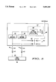
- FIG. 1 is a simplified block diagram of a light emitting device array with drive apparatus connected thereto;
- FIG. 2 is a simplified sectional view of a typical organic light emitting device
- FIG. 3 is block/schematic representation of a single addressed drive circuit
- FIG. 4 is a block/schematic representation of a single addressed drive circuit in accordance with the present invention.
- FIG. 5 is a simplified schematic/block diagram illustrating in more detail, drive circuits in accordance with the present invention.
- array 10 includes a plurality of organic light emitting devices (LEDs) connected into thirty two rows and sixty four columns. Thirty two row terminals 13 are illustrated at the left side of array 10 in FIG. 1 and sixty four column terminals 14 are illustrated at the top. While most of the discussion herein is directed to organic LED arrays because of their novel resistance problem, it should be understood that other types of LED arrays (i.e. semiconductor LEDs, LCDs, semiconductor laser arrays, etc., may have similar problems, in which case the present invention may be useful for these applications.
- LEDs organic light emitting devices
- organic LED 15 is illustrated in a simplified cross-sectional view in FIG. 2.
- organic LED 15 includes a substrate 17 which is formed of a transparent material, such as glass, quartz, or a hard plastic or the like. Even some semiconductor materials are transparent to light and may be utilized as substrate 17, in which instance some of the electronics may be integrated directly onto the substrate.
- a positive conductive layer 18 is patterned onto the upper surface of substrate 17 in any of the many well known procedures, e.g. using photoresist or the like.
- Conductive layer 18 is patterned into a plurality of parallel spaced apart columns terminating in terminals 14 (FIG. 1). While conductive layer 18 may be formed of any organic or inorganic conductors, such as conductive polyaniline (PANI) or indium-tin-oxide (ITO), which are substantially transparent to visible light, in this specific example, conductive layer 18 is provided as a layer of ITO.
- PANI conductive polyaniline
- ITO indium-tin-oxide
- a hole transport layer 19 is positioned on the upper surface of layer 18.
- layer 19 is deposited as a blanket deposition over the upper surface of layer 18 and any exposed portions of substrate 17, since only the portion of layer 19 which overlies layer 18 will be activated.
- An electron transport and light emission layer 20 is positioned over the upper surface of layer 19.
- a cathode is generally formed of a layer 22 of low work function metal/conductors or combination of metals/conductors, at least one of which typically has a low work function.
- the cathode (layer 22) is formed of low work function material, such as the commonly used lithium or magnesium, or the cathode may be a conductive metal incorporating cesium, calcium or the like.
- a list of some possible examples of materials for the organic layer or layers (e.g. 19 and 20) of the above described organic LEDs follows.
- some examples are: poly(p-phenylenevinylene) (PPV); poly(p-phenylene) (PPP); and poly 2-methoxy,5-(2'-ethylhexoxy)1,4-phenylenevinylene! (MEH-PPV).
- PPV poly(p-phenylenevinylene)
- PPP poly(p-phenylene)
- MEH-PPV 2-methoxy,5-(2'-ethylhexoxy)1,4-phenylenevinylene!
- an example is: 8-hydroxquinoline aluminum (ALQ).
- an example is: 2-(4-tert-butylphenyl)-5-(p-biphenylyl)-1,3,4-oxadiazole (butyl-PBD).
- a hole transport material some examples are: 4,4'-bis N-phenyl-N-(3-methylphenyl)amino!biphenyl (TPD); and 1,1-bis(4-di-p-tolyaminophenyl)cyclohexane.
- a fluorescent that may be used as a single layer or as a dopant to an organic charge transporting layer is coumarin 540, and a wide variety of fluorescent dyes.
- low work function metals include: Mg:In, Ca, and Mg:Ag.
- array 10 (FIG. 1) is described as having a single organic LED for each pixel of an image, it should be understood that additional LEDs can be connected in parallel for additional brightness or redundancy. Also, an example of the incorporation of multiple LEDs in a single pixel to produce multiple colors, or full color, is disclosed in U.S. Pat. No. 5,424,560, entitled “Integrated Multicolor Organic LED Array", issued Jun. 13, 1995 and assigned to the same assignee.
- Each LED in array 10 includes one or more layers of polymers or low molecular weight organic compounds, generally as described above.
- organic/polymer will be shortened to "organic” but it should be understood that this term is intend to encompass all polymers or low molecular weight organic compounds.
- the organic materials that form layers 19 and 20 are chosen for their combination of electrical, luminescent and color properties, and various combinations of hole injecting, hole transporting, electron injecting, electron transporting, and luminescent or emitting materials can be used.
- organic layers 19 and 20 do not conduct electrons well and the electron resistivities (e.g., approximately 10e -7 ) are much higher than the hole resistivities (e.g., approximately 10e -3 ) in the same material.
- electron transport layer 20 conducts electrons relatively well but does not conduct holes well and can thus be thought of as a hole blocking layer.
- generally light, or photons are generated when electrons and holes combine.
- drive apparatus 12 includes a circuit for periodically cycling through the 32 rows of array 10.
- this circuit is illustrated as a 32 bit shift register, row driver 25.
- Shift register, row driver 25 is connected to a controller 26, which supplies clock pulses and any other driving information which may be required.
- a 64 bit column driver 27 is connected to column terminals 14 and supplies image data thereto.
- column driver 27 includes an individual driver for each column terminal 14 and a buffer or the like for storing a complete row of image information.
- Column driver 27 is connected to controller 26 for receiving each new row of image information therefrom.
- Controller 26 includes a serial interface 28 which supplies image data to column driver 27 and which optionally receives video or image data from an external data input 30.
- Serial interface 28 is also connected to a RAM/ROM memory 32 and to a central processing unit (CPU) 33, or the like.
- CPU 33 controls both column drivers 27 and shift register 25 and utilizes memory 32 to generate images on array 10. It will of course be understood by those skilled in the art that a wide variety of circuits can be utilized to control array 10 and controller 26, along with shift register, row driver 25 and column drivers 27, are simply one embodiment utilized for purposes of explanation herein.
- Addressed drive circuit 40 includes a single column driver 42, which is a single selected or addressed driver from column drivers 27 of FIG. 1.
- Column driver 42 is connected to the light emitting device or devices of a pixel 43 (represented as a single light emitting diode) through an associated resistance 44 (which is considered a part of pixel 43 for this explanation).
- Associated resistance 44 represents the resistance of the column conductor for array 10, as well as the row conductor and any resistance of the LEDs themselves.
- array 10 is constructed with a light emitting device (e.g. device 15) connected between each crossing of each column conductor (terminals 14) and each row conductor (terminals 13).
- Conductive layer 18 is patterned on substrate 17 to form the column conductors and terminals 14.
- Layer 22 is patterned to form the row conductors and terminals 13.
- conductive layer 18 must be transparent to the light generated by the devices, it generally has a relatively high resistance.
- the maximum number of devices that will be conducting in a column at a time is one.
- each of the column conductors will carry a maximum current equal to the current conducted by one LED 15 (e.g. approximately 1-2 mA).
- the resistivity ranges from about 7.5 ohms/square to 400 ohms/square. While the resistivity can be lowered by increasing the thickness of the column conductors, there are problems with uniformity of ITO which can lead to device defects as the conductor is thickened.
- a typical column conductor formed of ITO may be approximately 50 ohms/square.
- the resistance along a column conductor between adjacent rows would then be about 80 ohms. Over 30 rows, at 80 ohms/row, this results in a total of over 2.4 kohms of resistance between the first and the last LED in the column.
- any number from zero to all of the devices connected into each row may be conducting simultaneously (depending upon the image) so that each of the row conductors (layer 22), may be required to carry the current of all of the devices (e.g. 64 ⁇ approximately 1-2 mA).
- the row conductors are generally formed of a metal having as low a resistance as practical.
- the resistance for a row conductor may still be as much as 5 ohms. If, for example, enough LEDs are conducting in a row to draw 100 mA of current, this 5 ohms of resistance produces a voltage drop of 0.5 volts from one end of the row conductor to the other.
- resistor 44 of each pixel (diode 43) in array 10 varies in accordance with its position, age, use, etc.
- Addressed drive circuit 40 further includes a single row driver 45, which is a single selected or addressed driver from shift register, row drivers 25 of FIG. 1. Row driver 45 is connected to a second terminal of pixel 43 to complete addressed circuit 40.
- a power supply 47 has one terminal connected to column driver 42 and a second terminal connected to row driver 45 as illustrated in FIG. 3. It will be understood by those skilled in the art that each pixel in array 10 has a unique address that is defined by a specific column driver and row driver, and the combination of the column driver, pixel and row driver form an addressed circuit which, by the act of addressing is connected to power supply 47.
- FIG. 3 has been provided and is representative of all or any of the pixels of array 10.
- the power consumption of addressed circuit 40 is determined by:
- P d is the total power consumption of circuit 40
- I is the current through circuit 40
- V d1 is the voltage dropped across column driver 42;
- V d2 is the voltage dropped across row driver 45;
- V D is the voltage dropped across pixel 43.
- V pp is the voltage provided by power supply 47.
- V pp the voltage provided by power supply 47, is directly related to the power consumption of the pixel.
- addressed drive circuit 40 including single column driver 42, pixel 43 (including resistance 44 and a light emitting device), and single row driver 45 are illustrated.
- Power supply 47 of FIG. 3 is replaced with a controllable or switching power supply 47' has one terminal connected to column driver 42 and a second terminal connected to row driver 45 as illustrated in FIG. 4.
- switching power supply 47' has a control terminal 48' adapted to receive control signals thereon for controlling the output power of switching power supply 47'.
- output power control is performed by controlling V pp , since the current ⁇ I ⁇ conducted through pixel 43 is substantially constant to achieve a constant lumination.
- a control circuit 49' is attached between addressed circuit 40 and control terminal 48' of switching power supply 47'.
- control circuit 49' is attached to column driver 42 to sense changes in voltage drop generally across resistance 44, since the other voltage drops are substantially constant. It should be understood, however, that other points of addressed circuit 40 might be utilized and other sensing devices might be utilized, e.g. a current sensor might be incorporated in addressed circuit 40.
- control circuit 49' provides a control signal at control terminal 48' to change the output power (voltage) to tend to maintain the voltage drop at column driver 42 substantially constant.
- Control circuit 49' provides a unique control signal to control terminal 48' of controllable power supply 47', whereby a unique amount of power is applied to each of the addressed circuits of array 10.
- each column driver 42 (only two illustrated for convenience) is connected by an ITO column conductor (resistor 44) to one side of a light emitting device 43, the other side of which is connected through row driver 45 (or drivers) to an electrical return.
- controllable power supply 47' is connected to supply power to light emitting devices 43 through each addressed column driver.
- controllable power supply 47' includes a regulated source of power, such as pulse width modulated voltage regulator 50', and a comparator 51' connected thereto for controlling the voltage or power output.
- Each control circuit 49' includes a diode 55' connected between one input of comparator 51' and the output of the associated column driver 42. Essentially, the voltage dropped across the addressed circuit 40 is applied to the input of comparator 51'. A reference voltage is applied to a second input of comparator 51' and, if the voltage dropped across the addressed circuit 40 exceeds the reference voltage, i.e. a unique control signal is applied to control terminal 48' of voltage regulator 50', the voltage supplied by voltage regulator 50' is adjusted accordingly, whereby a unique amount of power is applied to each of the addressed circuits of array 10.
- the novel circuit described dynamically controls the output power, or voltage, of the controllable power source by means of feedback compensation from the addressed circuit to controllable power source 47'.
- This feedback compensation provides optimized voltage to each addressed circuit which reduces driver power consumption. Total power consumption is also reduced because driver voltages are regulated by high efficiency controllable power source 47' Because of the small, optimized power consumption, the disclosed smart driver in combination with an array of light emitting devices is very useful in displays in portable electronic devices.
Landscapes
- Engineering & Computer Science (AREA)
- Physics & Mathematics (AREA)
- Computer Hardware Design (AREA)
- General Physics & Mathematics (AREA)
- Theoretical Computer Science (AREA)
- Electroluminescent Light Sources (AREA)
- Control Of Indicators Other Than Cathode Ray Tubes (AREA)
- Control Of El Displays (AREA)
Priority Applications (4)
| Application Number | Priority Date | Filing Date | Title |
|---|---|---|---|
| US08/660,827 US5684368A (en) | 1996-06-10 | 1996-06-10 | Smart driver for an array of LEDs |
| TW086105520A TW375726B (en) | 1996-06-10 | 1997-04-28 | Smart driver for an array of LEDs |
| JP9165112A JPH1063228A (ja) | 1996-06-10 | 1997-06-05 | Ledアレイのスマート・ドライバ |
| EP97109106A EP0813180A1 (en) | 1996-06-10 | 1997-06-05 | Smart driver for an array of LEDs with brightness compensation circuit |
Applications Claiming Priority (1)
| Application Number | Priority Date | Filing Date | Title |
|---|---|---|---|
| US08/660,827 US5684368A (en) | 1996-06-10 | 1996-06-10 | Smart driver for an array of LEDs |
Publications (1)
| Publication Number | Publication Date |
|---|---|
| US5684368A true US5684368A (en) | 1997-11-04 |
Family
ID=24651133
Family Applications (1)
| Application Number | Title | Priority Date | Filing Date |
|---|---|---|---|
| US08/660,827 Expired - Lifetime US5684368A (en) | 1996-06-10 | 1996-06-10 | Smart driver for an array of LEDs |
Country Status (4)
| Country | Link |
|---|---|
| US (1) | US5684368A (enExample) |
| EP (1) | EP0813180A1 (enExample) |
| JP (1) | JPH1063228A (enExample) |
| TW (1) | TW375726B (enExample) |
Cited By (30)
| Publication number | Priority date | Publication date | Assignee | Title |
|---|---|---|---|---|
| US5929845A (en) * | 1996-09-03 | 1999-07-27 | Motorola, Inc. | Image scanner and display apparatus |
| WO1999045558A1 (en) * | 1998-03-05 | 1999-09-10 | Fed Corporation | Blue and ultraviolet photolithography with organic light emitting devices |
| US5965901A (en) * | 1996-11-28 | 1999-10-12 | Cambridge Display Technology Ltd. | Electroluminescent devices with voltage drive scheme |
| US5990802A (en) * | 1998-05-18 | 1999-11-23 | Smartlite Communications, Inc. | Modular LED messaging sign panel and display system |
| WO2000043981A1 (en) * | 1999-01-21 | 2000-07-27 | Koninklijke Philips Electronics N.V. | Organic electroluminescent display device |
| WO2000051103A1 (en) * | 1999-02-26 | 2000-08-31 | Colorado Microdisplay, Inc. | Method and apparatus for independent control of brightness and color balance in display and illumination systems |
| WO2001027910A1 (en) | 1999-10-12 | 2001-04-19 | Koninklijke Philips Electronics N.V. | Led display device |
| WO2001027909A1 (en) * | 1999-10-14 | 2001-04-19 | Illumagraphics, Llc | Remotely programmable control device for use in electroluminescent displays and lighting systems |
| EP1071070A3 (en) * | 1999-07-21 | 2002-01-16 | Infineon Technologies North America Corp. | Low current drive of light emitting device |
| US20020070914A1 (en) * | 2000-12-12 | 2002-06-13 | Philips Electronics North America Corporation | Control and drive circuit arrangement for illumination performance enhancement with LED light sources |
| US6433488B1 (en) | 2001-01-02 | 2002-08-13 | Chi Mei Optoelectronics Corp. | OLED active driving system with current feedback |
| US6486860B1 (en) * | 1997-03-15 | 2002-11-26 | Dambach-Werke Gmbh | Display unit with an LED matrix |
| EP1282104A1 (en) * | 2001-08-02 | 2003-02-05 | Seiko Epson Corporation | Driving of data lines in active matrix display device and display device |
| US20030146784A1 (en) * | 2001-10-19 | 2003-08-07 | Lechevalier Robert | Method and clamping apparatus for securing a minimum reference voltage in a video display boost regulator |
| US20030169219A1 (en) * | 2001-10-19 | 2003-09-11 | Lechevalier Robert | System and method for exposure timing compensation for row resistance |
| US20030209721A1 (en) * | 2002-05-07 | 2003-11-13 | Toshiki Inoue | Semiconductor driver circuit, display device and method of adjusting brightness balance for display device |
| US20040061672A1 (en) * | 2002-09-27 | 2004-04-01 | Rich Page | Method and apparatus for driving light emitting polymer displays |
| US6847171B2 (en) * | 2001-12-21 | 2005-01-25 | Seiko Epson Corporation | Organic electroluminescent device compensated pixel driver circuit |
| US20050024298A1 (en) * | 2000-07-07 | 2005-02-03 | Seiko Epson Corporation | Circuit, driver circuit, organic electroluminescent display device electro-optical device, electronic apparatus, method of controlling the current supply to an organic electroluminescent pixel, and method for driving a circuit |
| US20050035933A1 (en) * | 2002-07-19 | 2005-02-17 | Stmicroelectronics S.A. | Automated adaptation of the supply voltage of a light-emitting display according to the desired luminance |
| WO2005088593A1 (en) | 2004-03-10 | 2005-09-22 | Koninklijke Philips Electronics N.V. | An active matrix display with reduction of power onsumption |
| EP1306826A4 (en) * | 2000-07-28 | 2006-07-05 | Nichia Corp | DISPLAY CONTROL AND DISPLAY DEVICE |
| US7088321B1 (en) * | 2001-03-30 | 2006-08-08 | Infocus Corporation | Method and apparatus for driving LED light sources for a projection display |
| CN100410992C (zh) * | 2001-08-02 | 2008-08-13 | 精工爱普生株式会社 | 电光装置及其驱动方法 |
| US20090091467A1 (en) * | 2007-10-09 | 2009-04-09 | Ries Ii Jack Leighton | Extended life led fixture |
| USRE42161E1 (en) | 1996-06-27 | 2011-02-22 | Relume Corporation | Power supply for light emitting diode array |
| US10255834B2 (en) * | 2015-07-23 | 2019-04-09 | X-Celeprint Limited | Parallel redundant chiplet system for controlling display pixels |
| CN110570814A (zh) * | 2019-09-16 | 2019-12-13 | 芯颖科技有限公司 | Pmoled显示屏的视效补偿方法、装置及存储介质 |
| IT202000027020A1 (it) * | 2020-11-12 | 2021-02-12 | D A C Engineering & Res S R L | Dispositivo elettronico modulare intelligente per la sterilizzazione di superfici ed oggetti |
| US11030969B2 (en) * | 2019-03-29 | 2021-06-08 | E Ink Corporation | Electro-optic displays and methods of driving the same |
Families Citing this family (1)
| Publication number | Priority date | Publication date | Assignee | Title |
|---|---|---|---|---|
| JP2001143867A (ja) | 1999-11-18 | 2001-05-25 | Nec Corp | 有機el駆動回路 |
Citations (9)
| Publication number | Priority date | Publication date | Assignee | Title |
|---|---|---|---|---|
| US4048632A (en) * | 1976-03-05 | 1977-09-13 | Rockwell International Corporation | Drive circuit for a display |
| US4447762A (en) * | 1981-07-09 | 1984-05-08 | Emi Limited | Electroluminescent displays |
| US4642524A (en) * | 1985-01-08 | 1987-02-10 | Hewlett-Packard Company | Inverse shadowing in electroluminescent displays |
| US4897639A (en) * | 1987-04-30 | 1990-01-30 | Fuji Photo Film Co., Ltd. | Image forming method and apparatus |
| US4967192A (en) * | 1987-04-22 | 1990-10-30 | Hitachi, Ltd. | Light-emitting element array driver circuit |
| US5184114A (en) * | 1982-11-04 | 1993-02-02 | Integrated Systems Engineering, Inc. | Solid state color display system and light emitting diode pixels therefor |
| US5424560A (en) * | 1994-05-31 | 1995-06-13 | Motorola, Inc. | Integrated multicolor organic led array |
| US5473222A (en) * | 1994-07-05 | 1995-12-05 | Delco Electronics Corporation | Active matrix vacuum fluorescent display with microprocessor integration |
| US5483503A (en) * | 1995-06-30 | 1996-01-09 | Durel Corporation | Split chip inverter for EL lamp |
Family Cites Families (8)
| Publication number | Priority date | Publication date | Assignee | Title |
|---|---|---|---|---|
| US4441106A (en) * | 1982-06-04 | 1984-04-03 | Northern Telecom Limited | Electrical display apparatus with reduced peak power consumption |
| EP0106550B1 (en) * | 1982-09-21 | 1989-04-12 | Fujitsu Limited | Method of driving a matrix type display |
| FR2632436B1 (fr) * | 1988-06-01 | 1991-02-15 | Commissariat Energie Atomique | Procede d'adressage d'un ecran matriciel fluorescent a micropointes |
| US5008657A (en) * | 1989-01-31 | 1991-04-16 | Varo, Inc. | Self adjusting matrix display |
| DE69119833T2 (de) * | 1990-07-13 | 1997-01-09 | Citizen Watch Co Ltd | Elektrooptisches Anzeigegerät |
| JPH05113770A (ja) * | 1991-10-22 | 1993-05-07 | Pioneer Electron Corp | マトリクス駆動画像表示装置 |
| JP3390214B2 (ja) * | 1993-07-19 | 2003-03-24 | パイオニア株式会社 | 表示装置の駆動回路 |
| JPH09115673A (ja) * | 1995-10-13 | 1997-05-02 | Sony Corp | 発光素子又は装置、及びその駆動方法 |
-
1996
- 1996-06-10 US US08/660,827 patent/US5684368A/en not_active Expired - Lifetime
-
1997
- 1997-04-28 TW TW086105520A patent/TW375726B/zh not_active IP Right Cessation
- 1997-06-05 EP EP97109106A patent/EP0813180A1/en not_active Withdrawn
- 1997-06-05 JP JP9165112A patent/JPH1063228A/ja active Pending
Patent Citations (9)
| Publication number | Priority date | Publication date | Assignee | Title |
|---|---|---|---|---|
| US4048632A (en) * | 1976-03-05 | 1977-09-13 | Rockwell International Corporation | Drive circuit for a display |
| US4447762A (en) * | 1981-07-09 | 1984-05-08 | Emi Limited | Electroluminescent displays |
| US5184114A (en) * | 1982-11-04 | 1993-02-02 | Integrated Systems Engineering, Inc. | Solid state color display system and light emitting diode pixels therefor |
| US4642524A (en) * | 1985-01-08 | 1987-02-10 | Hewlett-Packard Company | Inverse shadowing in electroluminescent displays |
| US4967192A (en) * | 1987-04-22 | 1990-10-30 | Hitachi, Ltd. | Light-emitting element array driver circuit |
| US4897639A (en) * | 1987-04-30 | 1990-01-30 | Fuji Photo Film Co., Ltd. | Image forming method and apparatus |
| US5424560A (en) * | 1994-05-31 | 1995-06-13 | Motorola, Inc. | Integrated multicolor organic led array |
| US5473222A (en) * | 1994-07-05 | 1995-12-05 | Delco Electronics Corporation | Active matrix vacuum fluorescent display with microprocessor integration |
| US5483503A (en) * | 1995-06-30 | 1996-01-09 | Durel Corporation | Split chip inverter for EL lamp |
Cited By (53)
| Publication number | Priority date | Publication date | Assignee | Title |
|---|---|---|---|---|
| USRE42161E1 (en) | 1996-06-27 | 2011-02-22 | Relume Corporation | Power supply for light emitting diode array |
| US5929845A (en) * | 1996-09-03 | 1999-07-27 | Motorola, Inc. | Image scanner and display apparatus |
| US5965901A (en) * | 1996-11-28 | 1999-10-12 | Cambridge Display Technology Ltd. | Electroluminescent devices with voltage drive scheme |
| US6486860B1 (en) * | 1997-03-15 | 2002-11-26 | Dambach-Werke Gmbh | Display unit with an LED matrix |
| WO1999045558A1 (en) * | 1998-03-05 | 1999-09-10 | Fed Corporation | Blue and ultraviolet photolithography with organic light emitting devices |
| US5990802A (en) * | 1998-05-18 | 1999-11-23 | Smartlite Communications, Inc. | Modular LED messaging sign panel and display system |
| WO2000043981A1 (en) * | 1999-01-21 | 2000-07-27 | Koninklijke Philips Electronics N.V. | Organic electroluminescent display device |
| WO2000051103A1 (en) * | 1999-02-26 | 2000-08-31 | Colorado Microdisplay, Inc. | Method and apparatus for independent control of brightness and color balance in display and illumination systems |
| US6618031B1 (en) | 1999-02-26 | 2003-09-09 | Three-Five Systems, Inc. | Method and apparatus for independent control of brightness and color balance in display and illumination systems |
| EP1071070A3 (en) * | 1999-07-21 | 2002-01-16 | Infineon Technologies North America Corp. | Low current drive of light emitting device |
| EP1138036A1 (en) * | 1999-10-12 | 2001-10-04 | Koninklijke Philips Electronics N.V. | Led display device |
| WO2001027910A1 (en) | 1999-10-12 | 2001-04-19 | Koninklijke Philips Electronics N.V. | Led display device |
| WO2001027909A1 (en) * | 1999-10-14 | 2001-04-19 | Illumagraphics, Llc | Remotely programmable control device for use in electroluminescent displays and lighting systems |
| US6943759B2 (en) | 2000-07-07 | 2005-09-13 | Seiko Epson Corporation | Circuit, driver circuit, organic electroluminescent display device electro-optical device, electronic apparatus, method of controlling the current supply to an organic electroluminescent pixel, and method for driving a circuit |
| US20050024298A1 (en) * | 2000-07-07 | 2005-02-03 | Seiko Epson Corporation | Circuit, driver circuit, organic electroluminescent display device electro-optical device, electronic apparatus, method of controlling the current supply to an organic electroluminescent pixel, and method for driving a circuit |
| EP1306826A4 (en) * | 2000-07-28 | 2006-07-05 | Nichia Corp | DISPLAY CONTROL AND DISPLAY DEVICE |
| US20020070914A1 (en) * | 2000-12-12 | 2002-06-13 | Philips Electronics North America Corporation | Control and drive circuit arrangement for illumination performance enhancement with LED light sources |
| US6888529B2 (en) | 2000-12-12 | 2005-05-03 | Koninklijke Philips Electronics N.V. | Control and drive circuit arrangement for illumination performance enhancement with LED light sources |
| US6433488B1 (en) | 2001-01-02 | 2002-08-13 | Chi Mei Optoelectronics Corp. | OLED active driving system with current feedback |
| US7088321B1 (en) * | 2001-03-30 | 2006-08-08 | Infocus Corporation | Method and apparatus for driving LED light sources for a projection display |
| US6989826B2 (en) | 2001-08-02 | 2006-01-24 | Seiko Epson Corporation | Driving of data lines used in unit circuit control |
| EP1282104A1 (en) * | 2001-08-02 | 2003-02-05 | Seiko Epson Corporation | Driving of data lines in active matrix display device and display device |
| US7466311B2 (en) | 2001-08-02 | 2008-12-16 | Seiko Epson Corporation | Driving of data lines used in unit circuit control |
| CN100410992C (zh) * | 2001-08-02 | 2008-08-13 | 精工爱普生株式会社 | 电光装置及其驱动方法 |
| US20030030602A1 (en) * | 2001-08-02 | 2003-02-13 | Seiko Epson Corporation | Driving of data lines used in unit circuit control |
| US20030146784A1 (en) * | 2001-10-19 | 2003-08-07 | Lechevalier Robert | Method and clamping apparatus for securing a minimum reference voltage in a video display boost regulator |
| WO2003034385A3 (en) * | 2001-10-19 | 2003-12-18 | Clare Micronix Integrated Syst | System and method for illumination timing compensation in response to row resistance |
| US20030169219A1 (en) * | 2001-10-19 | 2003-09-11 | Lechevalier Robert | System and method for exposure timing compensation for row resistance |
| US7019719B2 (en) * | 2001-10-19 | 2006-03-28 | Clare Micronix Integrated Systems, Inc. | Method and clamping apparatus for securing a minimum reference voltage in a video display boost regulator |
| US6847171B2 (en) * | 2001-12-21 | 2005-01-25 | Seiko Epson Corporation | Organic electroluminescent device compensated pixel driver circuit |
| US20030209721A1 (en) * | 2002-05-07 | 2003-11-13 | Toshiki Inoue | Semiconductor driver circuit, display device and method of adjusting brightness balance for display device |
| US7187008B2 (en) | 2002-05-07 | 2007-03-06 | Kabushiki Kaisha Toyota Jidoshokki | Semiconductor driver circuit, display device and method of adjusting brightness balance for display device |
| US7755580B2 (en) * | 2002-07-19 | 2010-07-13 | Stmicroelectronics S.A. | Automated adaptation of the supply voltage of a light-emitting display according to the desired luminance |
| US20050035933A1 (en) * | 2002-07-19 | 2005-02-17 | Stmicroelectronics S.A. | Automated adaptation of the supply voltage of a light-emitting display according to the desired luminance |
| US7009603B2 (en) * | 2002-09-27 | 2006-03-07 | Tdk Semiconductor, Corp. | Method and apparatus for driving light emitting polymer displays |
| US20040061672A1 (en) * | 2002-09-27 | 2004-04-01 | Rich Page | Method and apparatus for driving light emitting polymer displays |
| US20070182672A1 (en) * | 2004-03-10 | 2007-08-09 | Koninklijke Philips Electronics, N.V. | Active matrix display with reduction of power onsumption |
| WO2005088593A1 (en) | 2004-03-10 | 2005-09-22 | Koninklijke Philips Electronics N.V. | An active matrix display with reduction of power onsumption |
| US7777738B2 (en) | 2004-03-10 | 2010-08-17 | Koninklijke Philips Electronics N.V. | Active matrix display with reduction of power consumption |
| US20090128054A1 (en) * | 2007-10-09 | 2009-05-21 | Ries Ii Jack Leighton | Extended Life LED Fixture with Central Controller and LED Lamps |
| US20090128052A1 (en) * | 2007-10-09 | 2009-05-21 | Ries Ii Jack Leighton | Extended Life LED Fixture with Distributed Controller and Multi-Chip LEDS |
| US7839295B2 (en) | 2007-10-09 | 2010-11-23 | Abl Ip Holding Llc | Extended life LED fixture |
| US20090091467A1 (en) * | 2007-10-09 | 2009-04-09 | Ries Ii Jack Leighton | Extended life led fixture |
| US8237581B2 (en) | 2007-10-09 | 2012-08-07 | Abl Ip Holding Llc | Extended life LED fixture with central controller and multi-chip LEDs |
| US8237582B2 (en) | 2007-10-09 | 2012-08-07 | Abl Ip Holding Llc | Extended life LED fixture with distributed controller and multi-chip LEDs |
| US8242927B2 (en) | 2007-10-09 | 2012-08-14 | Abl Ip Holding Llc | Extended life LED fixture with central controller and LED lamps |
| US10255834B2 (en) * | 2015-07-23 | 2019-04-09 | X-Celeprint Limited | Parallel redundant chiplet system for controlling display pixels |
| US10395582B2 (en) * | 2015-07-23 | 2019-08-27 | X-Celeprint Limited | Parallel redundant chiplet system with printed circuits for reduced faults |
| US11030969B2 (en) * | 2019-03-29 | 2021-06-08 | E Ink Corporation | Electro-optic displays and methods of driving the same |
| US11398204B2 (en) * | 2019-03-29 | 2022-07-26 | E Ink Corporation | Electro-optic displays and methods of driving the same |
| CN110570814A (zh) * | 2019-09-16 | 2019-12-13 | 芯颖科技有限公司 | Pmoled显示屏的视效补偿方法、装置及存储介质 |
| IT202000027020A1 (it) * | 2020-11-12 | 2021-02-12 | D A C Engineering & Res S R L | Dispositivo elettronico modulare intelligente per la sterilizzazione di superfici ed oggetti |
| WO2022101940A1 (en) * | 2020-11-12 | 2022-05-19 | D.A.C. Engineering & Research S.R.L. | Modular electronic smart device for sterilizing surfaces and objects |
Also Published As
| Publication number | Publication date |
|---|---|
| JPH1063228A (ja) | 1998-03-06 |
| EP0813180A1 (en) | 1997-12-17 |
| TW375726B (en) | 1999-12-01 |
Similar Documents
| Publication | Publication Date | Title |
|---|---|---|
| US5684368A (en) | Smart driver for an array of LEDs | |
| US5719589A (en) | Organic light emitting diode array drive apparatus | |
| US6014119A (en) | Electroluminescent display device including active polymer layer | |
| US6177767B1 (en) | Luminescent device having drive-current controlled pixels and method therefor | |
| US6429601B1 (en) | Electroluminescent devices | |
| EP1444683B1 (en) | Display driver circuits for electro-optic displays | |
| US6911960B1 (en) | Active-type electroluminescent display | |
| US7956826B2 (en) | Electroluminescent display device to display low brightness uniformly | |
| US20020030647A1 (en) | Uniform active matrix oled displays | |
| KR20040075019A (ko) | 액티브 매트릭스 전자 발광 디스플레이 디바이스 | |
| JP2001075524A (ja) | 表示装置 | |
| JP4451779B2 (ja) | エレクトロルミネセントディスプレイ装置 | |
| JP2010541012A (ja) | 電流駆動型elディスプレイの電源電圧の動的適応 | |
| JP2005513555A (ja) | アクティブマトリクスエレクトロルミネッセンス表示装置 | |
| KR20010113635A (ko) | 정전류장치, 표시장치 및 그 구동방법 | |
| US7847766B2 (en) | Self-emission display apparatus and method of driving the same | |
| US7714514B1 (en) | Large area organic electroluminescent display using bimorph MEMS devices | |
| KR100446694B1 (ko) | 전류미러를 이용한 전계발광 표시소자의 전류구동장치 | |
| KR20040045444A (ko) | 매트릭스 디스플레이 | |
| CN1179586A (zh) | 发光器件阵列的灵活驱动器 | |
| KR100444693B1 (ko) | 펄스폭변조방식의 디스플레이 소자 구동방법 | |
| JP4501414B2 (ja) | 有機エレクトロルミネッセンス装置、及びその駆動方法、並びに電子機器 | |
| JPH10503605A (ja) | 表示装置 | |
| HK1069000B (en) | Display driver circuits for electro-optic displays | |
| JPH11274551A (ja) | Led装置とその駆動方法、光源、画像形成装置、画像読み取り装置、表示装置 |
Legal Events
| Date | Code | Title | Description |
|---|---|---|---|
| AS | Assignment |
Owner name: MOTOROLA, INC., ILLINOIS Free format text: ASSIGNMENT OF ASSIGNORS INTEREST;ASSIGNORS:WEI, CHENGPING;SO, FRANKY;NORMAN, MICHAEL P.;REEL/FRAME:008044/0305 Effective date: 19960607 |
|
| STCF | Information on status: patent grant |
Free format text: PATENTED CASE |
|
| FPAY | Fee payment |
Year of fee payment: 4 |
|
| FPAY | Fee payment |
Year of fee payment: 8 |
|
| FPAY | Fee payment |
Year of fee payment: 12 |
|
| AS | Assignment |
Owner name: MOTOROLA SOLUTIONS, INC., ILLINOIS Free format text: CHANGE OF NAME;ASSIGNOR:MOTOROLA, INC;REEL/FRAME:025909/0661 Effective date: 20110104 |
|
| AS | Assignment |
Owner name: MOTOROLA SOLUTIONS, INC., ILLINOIS Free format text: CHANGE OF NAME;ASSIGNOR:MOTOROLA, INC;REEL/FRAME:026081/0001 Effective date: 20110104 |
|
| AS | Assignment |
Owner name: UNIVERSAL DISPLAY CORPORATION, NEW JERSEY Free format text: ASSIGNMENT OF ASSIGNORS INTEREST;ASSIGNOR:MOTOROLA SOLUTIONS, INC.;REEL/FRAME:026620/0812 Effective date: 20110316 |