US5625282A - Constant current circuit for preventing latch-up - Google Patents
Constant current circuit for preventing latch-up Download PDFInfo
- Publication number
- US5625282A US5625282A US08/598,892 US59889296A US5625282A US 5625282 A US5625282 A US 5625282A US 59889296 A US59889296 A US 59889296A US 5625282 A US5625282 A US 5625282A
- Authority
- US
- United States
- Prior art keywords
- electrode
- transistor
- base
- collector
- circuit
- Prior art date
- Legal status (The legal status is an assumption and is not a legal conclusion. Google has not performed a legal analysis and makes no representation as to the accuracy of the status listed.)
- Expired - Fee Related
Links
Images


Classifications
-
- G—PHYSICS
- G05—CONTROLLING; REGULATING
- G05F—SYSTEMS FOR REGULATING ELECTRIC OR MAGNETIC VARIABLES
- G05F3/00—Non-retroactive systems for regulating electric variables by using an uncontrolled element, or an uncontrolled combination of elements, such element or such combination having self-regulating properties
- G05F3/02—Regulating voltage or current
- G05F3/08—Regulating voltage or current wherein the variable is dc
- G05F3/10—Regulating voltage or current wherein the variable is dc using uncontrolled devices with non-linear characteristics
- G05F3/16—Regulating voltage or current wherein the variable is dc using uncontrolled devices with non-linear characteristics being semiconductor devices
- G05F3/20—Regulating voltage or current wherein the variable is dc using uncontrolled devices with non-linear characteristics being semiconductor devices using diode- transistor combinations
- G05F3/26—Current mirrors
- G05F3/265—Current mirrors using bipolar transistors only
Definitions
- the present invention relates to a constant current circuit. More particularly, the present invention relates to a constant current circuit for preventing latch up generated at a constant current circuit in a PLL synthesizer IC used in a terminal equipment of a wireless telephone.
- FIG. 9 shows a location of the constant current circuit built in PLL used for the telephone terminal equipment, for instance.
- the constant current circuit is used in PLL synthesizer IC for supplying current for a charge pump circuit, a phase-comparison circuit, a prescaler circuit and so on.
- FIG. 7 shows a conventional constant current circuit.
- the constant current circuit has a capacitor X for preventing oscillation.
- This capacitor X is connected between a collector electrode an emitter electrode of a transistor Q1.
- An area 10 circumscribed by a chain line shows a part of an IC circuit including a base, an emitter, a collector of an oscillation transistor Q4 and the capacitor X of the constant current circuit.
- An area 12 circumscribed by a two-dot chain line shows a parasitic thyristor which is assumed to be formed between a point "a" and a point "d” in the area 10.
- This parasitic thyristor comprises a PNP parasitic transistor q1 and a NPN parasitic transistor q2.
- a resistor r1 is connected between an emitter of the transistor q1 and the point a which is connected to the voltage source Vcc via resistor R2
- a resistor r2 is connected between a base of transistor q1 and the point a
- a resistor r3 is connected between a base of the transistor q1 and the collector of transistor q1
- a resistor r4 is connected between the base of transistor q2 and the point d
- a collector of the transistor q2 is connected to the point d which is connected the ground.
- FIG. 8 shows an enlarged view of the thyristor elements actually formed on the IC.
- the thyristor elements are depicted in FIG. 7 as shown circumscribed by a two-dot chain line.
- a first N - well area is defined at a plane of substrate (P-sub).
- an N + area for base contact, a P + area for emitter contact, and a P + area for collector contact are defined.
- a second N - well area is defined adjacent to the first N - well area in the substrate P-sub. Then a dielectric layer is formed on the second N - well area and then an electrode is formed on the dielectric layer to make the capacitor X.
- the emitter electrode of the transistor Q4 is connected to the power supply potential node through a resistor R2, while both the base electrode and the collector electrode are connected to one of electrodes (conductive layer) of the capacitor X formed on the dielectric layer.
- the other electrode of capacitor X on the second N - well area is connected to a ground potential node via N area which is formed in the N - well area.
- the constant current circuit is formed on the IC using lateral type of transistors.
- FIG. 8 shows only the base, the emitter, the collector and the capacitor X, and the other parts are omitted for simplicity of explanation.
- a parasitic thyristor comprised of a PNP parasitic transistor q1 and a NPN parasitic transistor q2 are formed through nodes a, b, c and d in the first N - well area and the second N - well area in IC.
- This parasitic thyristor is depicted by the two-dot chain line in FIG. 7 between a power supply potential node and a ground potential node via the resistor R2.
- a parasitic thyristor circuit 12 is formed in addition to the usual IC circuit comprised of transistors Q4 and Q1 as shown in FIG. 8.
- a parasitic resistor r1 is connected between an emitter of the parasitic transistor q1 and the emitter layer P + of transistor Q4 (point a) which is connected to the power supply potential node via the resistor R2.
- a parasitic resistor r2 is connected between a base of the parasitic transistor q1 and the emitter layer P + of transistor Q4 (point a).
- a parasitic resistor r3 is connected between a collector and the base of the parasitic transistor q1.
- the collector and the base of the parasitic transistor q1 are connected to the base and the collector of the parasitic transistor q2, respectively.
- a parasitic resistor r4 is connected between a base of the parasitic transistor q2 and the ground potential node.
- An emitter of the parasitic transistor q2 is grounded directly via the point d and the N layer in the N - well area.
- a constant current circuit comprises a first current mirror circuit having a first pair of first conductive type transistors (Q4, Q3) which is formed in a first well area of a semiconductor substrate, wherein said first pair of transistors have respective emitter electrodes connected to a first power supply potential node; a second current mirror circuit having a second pair of second conductive type transistors (Q1, Q2) formed on a plane of the semiconductor substrate, wherein said second pair of transistors have respective emitter electrodes connected to a second power supply potential node and respective collector electrodes of said second pair of transistors are connected to collector electrodes of corresponding first pair of transistors; and a MOS type capacitor being connected between the collector electrodes of said first pair of transistors and being formed in a second well area of the semiconductor substrate which is adjacent to said first well area.
- a constant current circuit comprises a first current mirror circuit having a first pair of first conductive type transistors (Q4, Q3) which is formed in a first well area of a semiconductor substrate, wherein said first pair of transistors have respective emitter electrodes connected to a first power supply potential node; a second current mirror circuit having a second pair of second conductive type transistors (Q1, Q2) formed on a plane of the semiconductor substrate, wherein said second pair of transistors have respective emitter electrodes connected to a second power supply potential node via a resistor R and respective collector electrodes of said second pair of transistors are connected to collector electrodes of corresponding first pair of transistors; and a MOS type capacitor being connected between the collector electrodes of said first pair of transistors and being formed in a second well area of the semiconductor substrate which is adjacent to said first well area.
- a resistor R which is connected to the emitter of the transistor Q1 is formed on a plane of said substrate.
- a constant current circuit comprises a current mirror circuit comprised of a first conductive type transistor (Q5) whose base is connected to the base of said transistor (Q4), whose emitter is connected to a first power supply potential node and whose collector supplies a current to an outside circuit.
- a constant current circuit comprises a current mirror circuit including of a second conductive type transistor (Q8) whose base is connected to the base of said transistor (Q1), whose emitter is connected to a second power supply potential node and whose collector draws a current from an outside circuit.
- a constant current circuit comprises a pair of third current mirror circuits comprised of first conductive type transistors (Q5, Q6) whose bases are connected to the base of said transistor (Q4), whose both emitters are connected to a first power supply potential node; and a pair of fourth current mirror circuits comprised of second conductive type transistors (Q7, Q8), whose bases are connected each other and the collector of said transistor (Q7) is connected to the collector of the transistor (Q6), whose both emitters are connected to a second power supply potential node; wherein said collector of the transistor (Q5) supplies a current to an outside circuit, and said collector of the transistor (Q8) draws a current from an outside circuit.
- FIG. 1 shows a circuit configuration of a constant current circuit of a first embodiment of the present invention.
- FIG. 2 is an enlarged part of a constant current circuit actually formed on IC, which is circumscribed by a chain line in FIG. 1.
- FIG. 3 shows a circuit configuration of a constant current circuit of a second embodiment of the present invention.
- FIG. 4 is an enlarged part of a constant current circuit actually formed on IC, which is circumscribed by a chain line in FIG. 3.
- FIG. 5 shows a circuit configuration of a constant current circuit of a third embodiment of the present invention.
- FIG. 6 shows a circuit configuration of a constant current circuit of a fourth embodiment of the present invention.
- FIG. 7 shows a circuit configuration of a conventional constant current circuit.
- FIG. 8 is an enlarged part of a conventional constant current circuit actually formed on IC, which is circumscribed by a chain line in FIG. 7.
- FIG. 9 shows a conventional constant current circuit for supplying current to other circuits which are built in PLL synthesizer IC.
- FIG. 1 shows a circuit configuration of a constant current circuit for preventing latch up of a constant current circuit in a first embodiment of the present invention.
- the constant current circuit comprises a first mirror circuit comprised of transistors Q3 and Q4, a second mirror circuit comprised of transistors Q1 and Q2, a diode D1, a MOS capacitor X which is connected between the collector of transistor Q1 and the collector and base of the transistor Q2.
- the diode D1 has an anode electrode connected to a collector electrode of transistor Q4, and a cathode electrode connected to a collector electrode of transistor Q1.
- one end of the capacitor X is connected to the collector of the transistor Q4 and the other end is connected to the collector and base of the transistor Q2.
- This capacitor X is used for preventing oscillation.
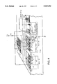
- FIG. 2 shows an actual construction of an IC of a constant current circuit in FIG. 1.
- FIG. 2 shows only the transistor Q4, the diode D1, the transistor Q1, and the capacitor X, which are formed on the substrate as lateral transistor structure, and other parts are omitted for simplicity of explanation.
- a parasitic thyristor comprised of the a PNP parasitic transistor q1 and a NPN parasitic transistor q2 are formed through nodes a, b, c and d in the first N - well which significantly influences the operation of the constant current circuit.
- This parasitic thyristor is depicted by the dotted line in FIG. 1 between a power supply potential node and a ground potential node via the resistor R2.
- a parasitic thyristor circuit 12 in FIG. 1 is formed in addition to the usual IC circuit comprised of transistors Q4 and Q1 as shown in FIG. 2.
- this parasitic thyristor has a similar construction as that in the prior art in FIG. 8, there is a significant difference from the prior art in that the emitter of parasitic transistor q2 of the parasitic thyristor is grounded directly in the prior art. Alternatively the emitter of parasitic transistor q2 of the parasitic thyristor is grounded via the base-emitter contact of the transistor Q1 in the present invention.
- a parasitic resistor r1 is connected between an emitter of parasitic transistor q1 and the emitter of the transistor Q4 (node a), while a parasitic resistor r2 is connected between a base of parasitic transistor q1 and the emitter of the transistor Q4 (node a). Furthermore, a parasitic resistor r3 is connected between the collector and the base of the parasitic transistor q1. The collector and the base of parasitic transistor q1 are connected to the base and the collector of parasitic transistor q2, respectively. The base of parasitic transistor q2 is connected to the ground potential node through parasitic resistor r4. The emitter of parasitic transistor q2 is grounded through the base-emitter contact of the transistor Q1.
- the parasitic transistor q1 turns on on the condition that the voltage drop of the parasitic resistor r2 is larger than V BE of the parasitic transistor q1.
- the parasitic transistor q2 turns on on the condition that the voltage drop of the parasitic resistor r4 is larger than 2V BE (voltage V BE between emitter and base of the parasitic transistor q2+voltage V BE between emitter and base of the transistor Q1).
- V BE voltage drop between emitter and base of the parasitic transistor q2+voltage V BE between emitter and base of the transistor Q1
- the condition which the parasitic transistor q1 turns on is the same, but the condition which the parasitic transistor q2 turns on is different from that of FIG. 7.
- FIG. 3 shows a circuit configuration of a constant current circuit for preventing latch up in a second embodiment of the present invention.
- the constant current circuit comprises a transistor Q4, a diode D1 having an anode which is connected to the collector of transistor Q4 and a cathode which is connected to a collector of transistor Q1, a MOS capacitor X which is connected between the collector of transistor Q1 and the collector and base of the transistor Q2, and a resistor R which is connected between an emitter electrode of transistor Q1 and a ground potential node.
- a parasitic thyristor is formed in the well area and the P-sub area, where a parasitic resistor r1 is connected between an emitter of the parasitic transistor q1 and the collector of transistor Q4 (point a) which is connected to the power supply potential node via the resistor R2.
- a parasitic resistor r2 is connected between a base (point b) of the parasitic transistor q1 and collector of transistor Q4 (point a) which is also connected to the power supply potential node via the resistor R2.
- a parasitic resistor r3 is connected between a collector and the base of the parasitic transistor q1. The collector and the base of the parasitic transistor q1 are connected to the base and the collector of the parasitic transistor q2, respectively.
- a parasitic resistor r4 is connected between a base of the parasitic transistor q2 and the ground potential node.
- An emitter of the parasitic transistor q2 is grounded via the base-emitter contact of transistor Q1 and a resistor R.
- the resistor R also is connected to the emitter of the transistor Q1.
- FIG. 4 is an enlarged part of a constant current circuit actually formed on IC, which is circumscribed by a chain line in FIG. 3.
- MOS capacitor X is formed on a second N - well area which is separated from P-sub by N + embedded layer, one of its electrodes is formed on a plane side (N in FIG. 3) of substrate, the other is formed on an electric conductive layer which is separated from a substrate by a dielectric layer.
- This capacitor X is used for preventing oscillation, one of its electrodes is connected to a collective electrode of transistor Q4, the other electrode is connected to a base electrode and a collector electrode of transistor Q2.
- FIG. 4 only transistor Q4, diode D1, transistor Q1, capacitor X and resistor R are shown, and the others are omitted for the simplicity of the explanation.
- a parasitic thyristor comprised of a PNP parasitic transistor q1 and a NPN parasitic transistor q2 is formed through nodes a, b, c and d in the first N - well area and the second N - well area in IC. This parasitic thyristor is depicted by the dotted line in FIG.
- a parasitic thyristor circuit 12 in FIG. 3 is formed in addition to the usual IC circuit comprised of transistors Q4 and Q1 as shown in FIG. 3.
- a parasitic resistor r1 is connected between an emitter of the parasitic transistor q1 and the emitter layer P + of transistor Q4 (point a) which is connected to the power supply potential node via the resistor R2.
- a parasitic resistor r2 is connected between a base of the parasitic transistor q1 and the emitter layer P + of transistor Q4 (point a) which is connected to the power supply potential node via the resistor R2.
- a parasitic resistor r3 is connected between a collector and the base of the parasitic transistor q1.
- the collector and the base of the parasitic transistor q1 are connected to the base and the collector of the parasitic transistor q2, respectively.
- a parasitic resistor r4 is connected between a base of the parasitic transistor q2 and the ground potential node.
- An emitter of the parasitic transistor q2 is grounded via the contact between the base and emitter of the transistor Q1 and the resistor R.
- the parasitic transistor q1 turns on on the condition that the voltage drop of the parasitic resistor r2 is larger than V BE of the parasitic transistor q1, which is the same as the description in FIG. 7.
- the parasitic transistor q2 turns on on the condition that the voltage drop of the parasitic resistor r4 is larger than 2 V BE (voltage V BE between emitter and base of the parasitic transistor q2+voltage V BE between emitter and base of the transistor Q1) plus the voltage drop V R of the resistor R.
- V BE voltage drop V BE between emitter and base of the parasitic transistor q2+voltage V BE between emitter and base of the transistor Q1
- V R of the resistor R is current i 2 ⁇ resistance of resistor R.
- the condition which the parasitic transistor q1 turns on is the same as that of the prior art (FIG.
- a third embodiment provides a constant current circuit which comprises transistors Q1 ⁇ Q4 and further comprises a transistor Q8.
- the third embodiment provides a constant current circuit for drawing current from outside circuit and for preventing latch up of the constant current circuit.
- FIG. 5 shows a circuit configuration of the constant current circuit for preventing latch up according to the third embodiment of the present invention.
- the constant current circuit in FIG. 5 comprises a basic circuit shown in FIG. 1 and an additional current mirror circuit.
- the basic circuit comprises a first pair of PNP transistors (Q4, Q3) and the second pair of NPN transistors (Q1, Q2).
- the current mirror circuit comprises an NPN transistor Q8, its base is connected to the base of the transistor Q1, and its emitter is connected to the ground potential via a resistor R7.
- the constant current circuit which comprises the transistors Q1 ⁇ Q4 and transistor Q8 draws the current from the outside circuit via the collector of the transistor Q8 which is the same current as that of the transistor Q1 by current mirror connection.
- Such construction prevents the constant current circuit comprised of the transistors Q1 ⁇ Q4 from stopping in the same way as described in the first embodiment, even in the case that high voltage is applied momentarily to the power supply potential node side. That is, the third constant current circuit draws the current from the outside circuit and also prevents the latch up of the constant current circuit.
- the constant current circuit is constructed not only for supplying the current to the outside circuit but also for drawing the current from the outside circuit.
- the constant current circuit in FIG. 6 comprises a basic circuit and an additional first and second current mirror circuits.
- the constant current circuit in FIG. 6 comprises a basic circuit in FIG. 1 and an additional first and second current mirror circuits.
- the basic circuit comprises a first pair of PNP transistors (Q4, Q3) and the second pair of NPN transistors (Q1, Q2).
- the first additional current mirror circuit comprises an NPN transistors Q5 and Q6 which are current mirrored to the transistor Q4.
- the second additional current mirror circuit comprises an NPN transistors Q7 and Q8, whose respective currents are the same as that of the transistor Q6.
- a base of the transistors Q6 and Q5 are connected to the base of the transistor Q4 and then the currents flowing in the collectors of the transistors Q6 and Q5, respectively, becomes the same as that of the transistor Q4.
- a collector of the transistor Q6 is connected to a collector of the transistor Q7, and its emitter is connected to the power supply via a resistor R5.
- An emitter of the transistor Q5 is connected to the power supply via a resistor R4 and its collector supplies a current to the outside circuit.
- a collector and a base of the transistor Q7 is connected each other and its emitter is connected to the ground potential via a resistor R6.
- An emitter of the transistor Q8 is connected to the ground potential via a resistor R7 and its collector draws current from the outside circuit.
- Such construction prevents the latch-up of the constant current circuit in the same way as explained in the first embodiment, even in the case where a high spike is applied momentarily to the power supply potential node side. That is, the fourth constant current circuit supplies and draws the currents to/from the outside circuit and also prevents the latch up of the constant current circuit.
- the elements having the same reference numbers in FIG. 6 as in FIG. 1 are explained above in connection with FIG. 1. Accordingly, a detailed explanation of those elements is not repeated.
- the transistors Q6, Q5 are current mirror connected to the transistor Q4, and the same current as that of transistor Q4 is supplied to the collector of transistor Q5.
- the collector of the transistor Q7 is connected to the collector of the transistor Q6, and the same current flows through the transistor Q7 as that of the transistor Q6. Since the transistor Q6 is current mirror connected to the transistor Q4, the current which is drawn from the collector of the transistor Q8 is the same as that of the transistor Q4. This construction also prevents the latch up of the constant current circuit.
Applications Claiming Priority (2)
| Application Number | Priority Date | Filing Date | Title |
|---|---|---|---|
| JP7-225152 | 1995-09-01 | ||
| JP7225152A JPH0969606A (ja) | 1995-09-01 | 1995-09-01 | 定電流回路 |
Publications (1)
| Publication Number | Publication Date |
|---|---|
| US5625282A true US5625282A (en) | 1997-04-29 |
Family
ID=16824767
Family Applications (1)
| Application Number | Title | Priority Date | Filing Date |
|---|---|---|---|
| US08/598,892 Expired - Fee Related US5625282A (en) | 1995-09-01 | 1996-02-09 | Constant current circuit for preventing latch-up |
Country Status (2)
| Country | Link |
|---|---|
| US (1) | US5625282A (ja) |
| JP (1) | JPH0969606A (ja) |
Cited By (5)
| Publication number | Priority date | Publication date | Assignee | Title |
|---|---|---|---|---|
| US5703478A (en) * | 1996-04-05 | 1997-12-30 | Motorola, Inc. | Current mirror circuit |
| US6137347A (en) * | 1998-11-04 | 2000-10-24 | Motorola, Ltd. | Mid supply reference generator |
| US6348835B1 (en) * | 1999-05-27 | 2002-02-19 | Nec Corporation | Semiconductor device with constant current source circuit not influenced by noise |
| US20040164790A1 (en) * | 2003-02-24 | 2004-08-26 | Samsung Electronics Co., Ltd. | Bias circuit having a start-up circuit |
| CN101013810B (zh) * | 2006-02-03 | 2011-04-06 | 西门子公司 | 用于识别短路或过电流的电路 |
Citations (7)
| Publication number | Priority date | Publication date | Assignee | Title |
|---|---|---|---|---|
| US4792750A (en) * | 1987-04-13 | 1988-12-20 | Teledyne Industries, Inc. | Resistorless, precision current source |
| US4950976A (en) * | 1989-09-29 | 1990-08-21 | Westinghouse Electric Corp. | Current variation reduction for mosfet current sources |
| US5223743A (en) * | 1991-04-26 | 1993-06-29 | Kabushiki Kaisha Toshiba | Adaptive current generating transconductance circuit |
| US5300765A (en) * | 1990-03-19 | 1994-04-05 | Mitsubishi Denki Kabushiki Kaisha | Memory card with latch-up protection |
| US5410242A (en) * | 1994-01-26 | 1995-04-25 | Micrel, Inc. | Capacitor and resistor connection in low voltage current source for splitting poles |
| US5481180A (en) * | 1991-09-30 | 1996-01-02 | Sgs-Thomson Microelectronics, Inc. | PTAT current source |
| US5521544A (en) * | 1993-11-16 | 1996-05-28 | Sharp Kabushiki Kaisha | Multiplier circuit having circuit wide dynamic range with reduced supply voltage requirements |
-
1995
- 1995-09-01 JP JP7225152A patent/JPH0969606A/ja active Pending
-
1996
- 1996-02-09 US US08/598,892 patent/US5625282A/en not_active Expired - Fee Related
Patent Citations (7)
| Publication number | Priority date | Publication date | Assignee | Title |
|---|---|---|---|---|
| US4792750A (en) * | 1987-04-13 | 1988-12-20 | Teledyne Industries, Inc. | Resistorless, precision current source |
| US4950976A (en) * | 1989-09-29 | 1990-08-21 | Westinghouse Electric Corp. | Current variation reduction for mosfet current sources |
| US5300765A (en) * | 1990-03-19 | 1994-04-05 | Mitsubishi Denki Kabushiki Kaisha | Memory card with latch-up protection |
| US5223743A (en) * | 1991-04-26 | 1993-06-29 | Kabushiki Kaisha Toshiba | Adaptive current generating transconductance circuit |
| US5481180A (en) * | 1991-09-30 | 1996-01-02 | Sgs-Thomson Microelectronics, Inc. | PTAT current source |
| US5521544A (en) * | 1993-11-16 | 1996-05-28 | Sharp Kabushiki Kaisha | Multiplier circuit having circuit wide dynamic range with reduced supply voltage requirements |
| US5410242A (en) * | 1994-01-26 | 1995-04-25 | Micrel, Inc. | Capacitor and resistor connection in low voltage current source for splitting poles |
Cited By (5)
| Publication number | Priority date | Publication date | Assignee | Title |
|---|---|---|---|---|
| US5703478A (en) * | 1996-04-05 | 1997-12-30 | Motorola, Inc. | Current mirror circuit |
| US6137347A (en) * | 1998-11-04 | 2000-10-24 | Motorola, Ltd. | Mid supply reference generator |
| US6348835B1 (en) * | 1999-05-27 | 2002-02-19 | Nec Corporation | Semiconductor device with constant current source circuit not influenced by noise |
| US20040164790A1 (en) * | 2003-02-24 | 2004-08-26 | Samsung Electronics Co., Ltd. | Bias circuit having a start-up circuit |
| CN101013810B (zh) * | 2006-02-03 | 2011-04-06 | 西门子公司 | 用于识别短路或过电流的电路 |
Also Published As
| Publication number | Publication date |
|---|---|
| JPH0969606A (ja) | 1997-03-11 |
Similar Documents
| Publication | Publication Date | Title |
|---|---|---|
| US5838043A (en) | ESD protection circuit located under protected bonding pad | |
| JP2850801B2 (ja) | 半導体素子 | |
| US7570467B2 (en) | Electrostatic protection circuit | |
| US4453092A (en) | Comparator circuit having reduced input bias current | |
| JP2005192302A (ja) | チャージポンプ回路 | |
| US4027271A (en) | Capacitor structure and circuit facilitating increased frequency stability of integrated circuits | |
| US5625282A (en) | Constant current circuit for preventing latch-up | |
| JPH10173128A (ja) | 接合が絶縁された集積回路の寄生効果を抑制する方法および装置 | |
| US5973901A (en) | Semiconductor circuit device with high electrostatic breakdown endurance | |
| US7485931B2 (en) | Semiconductor integrated circuit | |
| KR100502379B1 (ko) | 3중웰기술을이용하는고밀도dram용esd보호회로 | |
| JP2636804B2 (ja) | 半導体装置 | |
| US4723081A (en) | CMOS integrated circuit protected from latch-up phenomenon | |
| US6894881B1 (en) | ESD protection methods and devices using additional terminal in the diode structures | |
| US5821601A (en) | Bipolar semiconductor integrated circuit with a protection circuit | |
| US5237195A (en) | Semiconductor integrated circuit arrangement for preventing latch up | |
| US6337501B1 (en) | Semiconductor device having bipolar transistor and MOS transistor | |
| US6850111B1 (en) | Charge pump circuit | |
| JP3179630B2 (ja) | エピタキシャル・タブ・バイアス構体及び集積回路 | |
| US5382837A (en) | Switching circuit for semiconductor device | |
| EP0607474B1 (en) | Semiconductor integrated circuit with layer for isolating elements in substrate | |
| JP3387940B2 (ja) | 電源バックアップ用半導体装置 | |
| US6424201B2 (en) | Diode element circuit and switch circuit using the same | |
| JP3241698B2 (ja) | 半導体集積回路装置 | |
| JPH05291507A (ja) | 拡散抵抗 |
Legal Events
| Date | Code | Title | Description |
|---|---|---|---|
| AS | Assignment |
Owner name: MITSUBISHI DENKI KABUSHIKI KAISHA, JAPAN Free format text: ASSIGNMENT OF ASSIGNORS INTEREST;ASSIGNOR:KAWAHARA, TADASHI;REEL/FRAME:007858/0786 Effective date: 19960124 |
|
| CC | Certificate of correction | ||
| FEPP | Fee payment procedure |
Free format text: PAYOR NUMBER ASSIGNED (ORIGINAL EVENT CODE: ASPN); ENTITY STATUS OF PATENT OWNER: LARGE ENTITY |
|
| FEPP | Fee payment procedure |
Free format text: PAYER NUMBER DE-ASSIGNED (ORIGINAL EVENT CODE: RMPN); ENTITY STATUS OF PATENT OWNER: LARGE ENTITY Free format text: PAYOR NUMBER ASSIGNED (ORIGINAL EVENT CODE: ASPN); ENTITY STATUS OF PATENT OWNER: LARGE ENTITY |
|
| FPAY | Fee payment |
Year of fee payment: 4 |
|
| FPAY | Fee payment |
Year of fee payment: 8 |
|
| REMI | Maintenance fee reminder mailed | ||
| LAPS | Lapse for failure to pay maintenance fees | ||
| STCH | Information on status: patent discontinuation |
Free format text: PATENT EXPIRED DUE TO NONPAYMENT OF MAINTENANCE FEES UNDER 37 CFR 1.362 |
|
| FP | Lapsed due to failure to pay maintenance fee |
Effective date: 20090429 |