US5561320A - Silver spot/palladium plate lead frame finish - Google Patents
Silver spot/palladium plate lead frame finish Download PDFInfo
- Publication number
- US5561320A US5561320A US08/329,024 US32902494A US5561320A US 5561320 A US5561320 A US 5561320A US 32902494 A US32902494 A US 32902494A US 5561320 A US5561320 A US 5561320A
- Authority
- US
- United States
- Prior art keywords
- lead frame
- palladium
- layer
- silver
- leads
- Prior art date
- Legal status (The legal status is an assumption and is not a legal conclusion. Google has not performed a legal analysis and makes no representation as to the accuracy of the status listed.)
- Expired - Lifetime
Links
Images

Classifications
-
- C—CHEMISTRY; METALLURGY
- C23—COATING METALLIC MATERIAL; COATING MATERIAL WITH METALLIC MATERIAL; CHEMICAL SURFACE TREATMENT; DIFFUSION TREATMENT OF METALLIC MATERIAL; COATING BY VACUUM EVAPORATION, BY SPUTTERING, BY ION IMPLANTATION OR BY CHEMICAL VAPOUR DEPOSITION, IN GENERAL; INHIBITING CORROSION OF METALLIC MATERIAL OR INCRUSTATION IN GENERAL
- C23C—COATING METALLIC MATERIAL; COATING MATERIAL WITH METALLIC MATERIAL; SURFACE TREATMENT OF METALLIC MATERIAL BY DIFFUSION INTO THE SURFACE, BY CHEMICAL CONVERSION OR SUBSTITUTION; COATING BY VACUUM EVAPORATION, BY SPUTTERING, BY ION IMPLANTATION OR BY CHEMICAL VAPOUR DEPOSITION, IN GENERAL
- C23C28/00—Coating for obtaining at least two superposed coatings either by methods not provided for in a single one of groups C23C2/00 - C23C26/00 or by combinations of methods provided for in subclasses C23C and C25C or C25D
- C23C28/02—Coating for obtaining at least two superposed coatings either by methods not provided for in a single one of groups C23C2/00 - C23C26/00 or by combinations of methods provided for in subclasses C23C and C25C or C25D only coatings only including layers of metallic material
- C23C28/023—Coating for obtaining at least two superposed coatings either by methods not provided for in a single one of groups C23C2/00 - C23C26/00 or by combinations of methods provided for in subclasses C23C and C25C or C25D only coatings only including layers of metallic material only coatings of metal elements only
-
- H—ELECTRICITY
- H10—SEMICONDUCTOR DEVICES; ELECTRIC SOLID-STATE DEVICES NOT OTHERWISE PROVIDED FOR
- H10W—GENERIC PACKAGES, INTERCONNECTIONS, CONNECTORS OR OTHER CONSTRUCTIONAL DETAILS OF DEVICES COVERED BY CLASS H10
- H10W70/00—Package substrates; Interposers; Redistribution layers [RDL]
- H10W70/40—Leadframes
- H10W70/456—Materials
- H10W70/457—Materials of metallic layers on leadframes
-
- H—ELECTRICITY
- H10—SEMICONDUCTOR DEVICES; ELECTRIC SOLID-STATE DEVICES NOT OTHERWISE PROVIDED FOR
- H10W—GENERIC PACKAGES, INTERCONNECTIONS, CONNECTORS OR OTHER CONSTRUCTIONAL DETAILS OF DEVICES COVERED BY CLASS H10
- H10W72/00—Interconnections or connectors in packages
- H10W72/071—Connecting or disconnecting
- H10W72/075—Connecting or disconnecting of bond wires
-
- H—ELECTRICITY
- H10—SEMICONDUCTOR DEVICES; ELECTRIC SOLID-STATE DEVICES NOT OTHERWISE PROVIDED FOR
- H10W—GENERIC PACKAGES, INTERCONNECTIONS, CONNECTORS OR OTHER CONSTRUCTIONAL DETAILS OF DEVICES COVERED BY CLASS H10
- H10W72/00—Interconnections or connectors in packages
- H10W72/50—Bond wires
- H10W72/551—Materials of bond wires
- H10W72/552—Materials of bond wires comprising metals or metalloids, e.g. silver
- H10W72/5522—Materials of bond wires comprising metals or metalloids, e.g. silver comprising gold [Au]
-
- H—ELECTRICITY
- H10—SEMICONDUCTOR DEVICES; ELECTRIC SOLID-STATE DEVICES NOT OTHERWISE PROVIDED FOR
- H10W—GENERIC PACKAGES, INTERCONNECTIONS, CONNECTORS OR OTHER CONSTRUCTIONAL DETAILS OF DEVICES COVERED BY CLASS H10
- H10W72/00—Interconnections or connectors in packages
- H10W72/50—Bond wires
- H10W72/59—Bond pads specially adapted therefor
-
- H—ELECTRICITY
- H10—SEMICONDUCTOR DEVICES; ELECTRIC SOLID-STATE DEVICES NOT OTHERWISE PROVIDED FOR
- H10W—GENERIC PACKAGES, INTERCONNECTIONS, CONNECTORS OR OTHER CONSTRUCTIONAL DETAILS OF DEVICES COVERED BY CLASS H10
- H10W72/00—Interconnections or connectors in packages
- H10W72/90—Bond pads, in general
- H10W72/951—Materials of bond pads
- H10W72/952—Materials of bond pads comprising metals or metalloids, e.g. PbSn, Ag or Cu
-
- H—ELECTRICITY
- H10—SEMICONDUCTOR DEVICES; ELECTRIC SOLID-STATE DEVICES NOT OTHERWISE PROVIDED FOR
- H10W—GENERIC PACKAGES, INTERCONNECTIONS, CONNECTORS OR OTHER CONSTRUCTIONAL DETAILS OF DEVICES COVERED BY CLASS H10
- H10W90/00—Package configurations
- H10W90/701—Package configurations characterised by the relative positions of pads or connectors relative to package parts
- H10W90/751—Package configurations characterised by the relative positions of pads or connectors relative to package parts of bond wires
- H10W90/756—Package configurations characterised by the relative positions of pads or connectors relative to package parts of bond wires between a chip and a stacked lead frame, conducting package substrate or heat sink
Definitions
- This invention relates to semiconductor devices, and more particularly to spot plating selected parts of a lead frame to improve bonding.
- Certain assembly operation schemes for integrated circuits require low processing temperatures which may limit the ability to bond to the standard palladium finish.
- certain lead frame designs mandated by finish device requirements, limit the amount of heat that can be applied to a lead frame in the bonding operation, or restrict the ability to clamp and immobilize the lead fingers during the bond operation.
- Lead on chip is an example of this type of lead frame design.
- the invention is a method of spot plating silver on palladium for the parts of the lead frame that are internal to the plastic package holding a semiconductor device.
- a spot of silver is plated in the mount and/or bond areas of a lead frame.
- the entire lead frame is first plated with palladium/nickel finish prior to spot silver plating.
- FIG. 1 is a flow diagram of the process of the present invention
- FIG. 2 illustrates a typical semiconductor lead frame
- FIG. 3 is an enlarged portion of the lead frame of FIG. 2 showing the spot plating.
- FIG. 1 is a flow diagram of the present invention.
- a lead frame, step 10, for example, of copper alloy, alloy 42 or other base metal is plated (step 11) with a palladium finish or a similar palladium-nickel or palladium strike or flash, nickel plate, or thin palladium plate.
- An optional layer of copper or another metal is applied at selected places on the lead frame (step 12).
- a layer of silver, or another metal is applied to selected spots on the lead frame to improve wire bondability of gold wire to the lead frame.
- the gold, or other metal, wire is bonded to the silver spots.
- Metals other than silver may be used.
- the silver over palladium or palladium alloy provides improved package integrity.
- the amount of silver required may be reduced when silver is spot plated over palladium rather than a base metal.
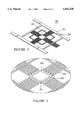
- FIG. 2 is a typical semiconductor lead frame 20 having a device mounting pad 22, leads 23 on a continuous lead frame strip 21.
- FIG. 3 is an enlarged portion of FIG. 2, illustrating the device mounting pad 22 and leads 23.
- a portion of the mounting pad 22 has a layer of silver 24 thereon.
- leads 23 each have a layer of silver plating 25 on the end of each lead. This facilitates attaching a gold bond wire to the tip of each lead and to a bond pad on a device (not illustrated) that will be mounted on the mounting pad.
Landscapes
- Chemical & Material Sciences (AREA)
- Chemical Kinetics & Catalysis (AREA)
- Engineering & Computer Science (AREA)
- Materials Engineering (AREA)
- Mechanical Engineering (AREA)
- Metallurgy (AREA)
- Organic Chemistry (AREA)
- Lead Frames For Integrated Circuits (AREA)
- Electroplating Methods And Accessories (AREA)
Abstract
A lead frame is plated with palladium and then selected portions of the lead frame leads are spot plated with silver to improve solderability.
Description
This is a division of application Ser. No. 07/893,911, filed Jun. 4, 1992, now U.S. Pat. No. 5,384,155.
This invention relates to semiconductor devices, and more particularly to spot plating selected parts of a lead frame to improve bonding.
Certain assembly operation schemes for integrated circuits require low processing temperatures which may limit the ability to bond to the standard palladium finish. Similarly, certain lead frame designs mandated by finish device requirements, limit the amount of heat that can be applied to a lead frame in the bonding operation, or restrict the ability to clamp and immobilize the lead fingers during the bond operation. Lead on chip is an example of this type of lead frame design.
The invention is a method of spot plating silver on palladium for the parts of the lead frame that are internal to the plastic package holding a semiconductor device. A spot of silver is plated in the mount and/or bond areas of a lead frame. The entire lead frame is first plated with palladium/nickel finish prior to spot silver plating.
The technical advance represented by the invention as well as the objects thereof will become apparent from the following description of a preferred embodiment of the invention when considered in conjunction with the accompanying drawings, and the novel features set forth in the appended claims.
FIG. 1 is a flow diagram of the process of the present invention;
FIG. 2 illustrates a typical semiconductor lead frame; and
FIG. 3 is an enlarged portion of the lead frame of FIG. 2 showing the spot plating.
FIG. 1 is a flow diagram of the present invention. A lead frame, step 10, for example, of copper alloy, alloy 42 or other base metal is plated (step 11) with a palladium finish or a similar palladium-nickel or palladium strike or flash, nickel plate, or thin palladium plate.
An optional layer of copper or another metal is applied at selected places on the lead frame (step 12).
After the previous plating steps, a layer of silver, or another metal, is applied to selected spots on the lead frame to improve wire bondability of gold wire to the lead frame. The gold, or other metal, wire is bonded to the silver spots. Metals other than silver may be used.
The silver over palladium or palladium alloy provides improved package integrity. The amount of silver required may be reduced when silver is spot plated over palladium rather than a base metal.
FIG. 2 is a typical semiconductor lead frame 20 having a device mounting pad 22, leads 23 on a continuous lead frame strip 21.
FIG. 3 is an enlarged portion of FIG. 2, illustrating the device mounting pad 22 and leads 23. A portion of the mounting pad 22 has a layer of silver 24 thereon. Also leads 23 each have a layer of silver plating 25 on the end of each lead. This facilitates attaching a gold bond wire to the tip of each lead and to a bond pad on a device (not illustrated) that will be mounted on the mounting pad.
Claims (6)
1. A lead frame for a semiconductor device including a device mounting pad and lead frame leads, said lead frame comprising;
a layer of first metal selected from the group consisting of palladium and palladium-nickel plated on said lead frame;
a spot plating of silver on selected portions of said lead frame leads; and
a plating of copper between said first metal plated on said lead frame and said spot plating of silver.
2. The lead frame of claim 1, wherein said layer of first metal comprises palladium.
3. The lead frame of claim 1, wherein said layer of first metal comprises a layer of palladium nickel alloy.
4. The lead frame of claim 1, wherein the selected portions of said lead frame leads include the ends of said lead frame leads which are to be attached to a semiconductor device.
5. A lead frame for a semiconductor device including a device mounting pad and lead frame leads, comprising:
a layer of palladium over a lead frame substrate;
a spot plating of silver placed over selected portions of said lead frame leads, said selected portions being within the plastic package after encapsulation; and
a plating of copper placed between said layer of palladium and said spot plating of silver at said selected portions of said lead frame leads.
6. The lead frame of claim 5, wherein said layer of palladium comprises a layer of nickel-palladium alloy.
Priority Applications (2)
| Application Number | Priority Date | Filing Date | Title |
|---|---|---|---|
| US08/329,024 US5561320A (en) | 1992-06-04 | 1994-10-25 | Silver spot/palladium plate lead frame finish |
| US08/483,664 US5710456A (en) | 1992-06-04 | 1995-06-07 | Silver spot/palladium plate lead frame finish |
Applications Claiming Priority (2)
| Application Number | Priority Date | Filing Date | Title |
|---|---|---|---|
| US07/893,911 US5384155A (en) | 1992-06-04 | 1992-06-04 | Silver spot/palladium plate lead frame finish |
| US08/329,024 US5561320A (en) | 1992-06-04 | 1994-10-25 | Silver spot/palladium plate lead frame finish |
Related Parent Applications (1)
| Application Number | Title | Priority Date | Filing Date |
|---|---|---|---|
| US07/893,911 Division US5384155A (en) | 1992-06-04 | 1992-06-04 | Silver spot/palladium plate lead frame finish |
Related Child Applications (1)
| Application Number | Title | Priority Date | Filing Date |
|---|---|---|---|
| US08/483,664 Division US5710456A (en) | 1992-06-04 | 1995-06-07 | Silver spot/palladium plate lead frame finish |
Publications (1)
| Publication Number | Publication Date |
|---|---|
| US5561320A true US5561320A (en) | 1996-10-01 |
Family
ID=25402323
Family Applications (3)
| Application Number | Title | Priority Date | Filing Date |
|---|---|---|---|
| US07/893,911 Expired - Lifetime US5384155A (en) | 1992-06-04 | 1992-06-04 | Silver spot/palladium plate lead frame finish |
| US08/329,024 Expired - Lifetime US5561320A (en) | 1992-06-04 | 1994-10-25 | Silver spot/palladium plate lead frame finish |
| US08/483,664 Expired - Lifetime US5710456A (en) | 1992-06-04 | 1995-06-07 | Silver spot/palladium plate lead frame finish |
Family Applications Before (1)
| Application Number | Title | Priority Date | Filing Date |
|---|---|---|---|
| US07/893,911 Expired - Lifetime US5384155A (en) | 1992-06-04 | 1992-06-04 | Silver spot/palladium plate lead frame finish |
Family Applications After (1)
| Application Number | Title | Priority Date | Filing Date |
|---|---|---|---|
| US08/483,664 Expired - Lifetime US5710456A (en) | 1992-06-04 | 1995-06-07 | Silver spot/palladium plate lead frame finish |
Country Status (1)
| Country | Link |
|---|---|
| US (3) | US5384155A (en) |
Cited By (12)
| Publication number | Priority date | Publication date | Assignee | Title |
|---|---|---|---|---|
| US5710456A (en) * | 1992-06-04 | 1998-01-20 | Texas Instruments Incorporated | Silver spot/palladium plate lead frame finish |
| US5767574A (en) * | 1996-03-26 | 1998-06-16 | Samsung Aerospace Industries, Ltd. | Semiconductor lead frame |
| DE19741921A1 (en) * | 1997-09-23 | 1999-02-25 | Siemens Ag | Carrier element for semiconductor chip card data type carrier |
| US5923081A (en) * | 1997-05-15 | 1999-07-13 | Micron Technology, Inc. | Compression layer on the leadframe to reduce stress defects |
| US5925930A (en) * | 1996-05-21 | 1999-07-20 | Micron Technology, Inc. | IC contacts with palladium layer and flexible conductive epoxy bumps |
| US6544880B1 (en) | 1999-06-14 | 2003-04-08 | Micron Technology, Inc. | Method of improving copper interconnects of semiconductor devices for bonding |
| US6558979B2 (en) | 1996-05-21 | 2003-05-06 | Micron Technology, Inc. | Use of palladium in IC manufacturing with conductive polymer bump |
| US20100155770A1 (en) * | 2003-01-16 | 2010-06-24 | Panasonic Corporation | Multilayered lead frame for a semiconductor light-emitting device |
| US9025285B1 (en) | 2009-12-16 | 2015-05-05 | Magnecomp Corporation | Low resistance interface metal for disk drive suspension component grounding |
| CN105702656A (en) * | 2014-12-10 | 2016-06-22 | 意法半导体私人公司 | Integrated circuit device with plating on lead interconnection point and method of forming the device |
| US9583125B1 (en) | 2009-12-16 | 2017-02-28 | Magnecomp Corporation | Low resistance interface metal for disk drive suspension component grounding |
| CN110528036A (en) * | 2019-08-29 | 2019-12-03 | 深圳市崇辉表面技术开发有限公司 | A kind of LED bracket electroplating method and LED bracket |
Families Citing this family (17)
| Publication number | Priority date | Publication date | Assignee | Title |
|---|---|---|---|---|
| US5673845A (en) * | 1996-06-17 | 1997-10-07 | Micron Technology, Inc. | Lead penetrating clamping system |
| US5890644A (en) | 1996-01-26 | 1999-04-06 | Micron Technology, Inc. | Apparatus and method of clamping semiconductor devices using sliding finger supports |
| US5647528A (en) | 1996-02-06 | 1997-07-15 | Micron Technology, Inc. | Bondhead lead clamp apparatus and method |
| US6407333B1 (en) * | 1997-11-04 | 2002-06-18 | Texas Instruments Incorporated | Wafer level packaging |
| US6068174A (en) | 1996-12-13 | 2000-05-30 | Micro)N Technology, Inc. | Device and method for clamping and wire-bonding the leads of a lead frame one set at a time |
| US6157074A (en) * | 1997-07-16 | 2000-12-05 | Hyundai Electronics Industries Co., Ltd. | Lead frame adapted for variable sized devices, semiconductor package with such lead frame and method for using same |
| US6180999B1 (en) * | 1997-08-29 | 2001-01-30 | Texas Instruments Incorporated | Lead-free and cyanide-free plating finish for semiconductor lead frames |
| US6121674A (en) * | 1998-02-23 | 2000-09-19 | Micron Technology, Inc. | Die paddle clamping method for wire bond enhancement |
| US6126062A (en) * | 1998-04-02 | 2000-10-03 | Micron Technology, Inc. | Non-conductive and self-leveling leadframe clamp insert for wirebonding integrated circuits |
| US6634538B2 (en) | 1998-04-02 | 2003-10-21 | Micron Technology, Inc. | Non-conductive and self-leveling leadframe clamp insert for wirebonding integrated circuits |
| US6977214B2 (en) * | 1998-12-11 | 2005-12-20 | Micron Technology, Inc. | Die paddle clamping method for wire bond enhancement |
| KR100371567B1 (en) * | 2000-12-08 | 2003-02-07 | 삼성테크윈 주식회사 | Ag pre-plated lead frame for semiconductor package |
| US7859392B2 (en) | 2006-05-22 | 2010-12-28 | Iwi, Inc. | System and method for monitoring and updating speed-by-street data |
| JP4834022B2 (en) * | 2007-03-27 | 2011-12-07 | 古河電気工業株式会社 | Silver coating material for movable contact parts and manufacturing method thereof |
| CN101295695A (en) * | 2007-04-29 | 2008-10-29 | 飞思卡尔半导体(中国)有限公司 | Leadframe with Solder Flow Control |
| KR101217308B1 (en) * | 2011-05-27 | 2012-12-31 | 앰코 테크놀로지 코리아 주식회사 | Lead frame for semiconductor device |
| US9230928B2 (en) * | 2011-09-12 | 2016-01-05 | Conexant Systems, Inc. | Spot plated leadframe and IC bond pad via array design for copper wire |
Citations (13)
| Publication number | Priority date | Publication date | Assignee | Title |
|---|---|---|---|---|
| JPS59219952A (en) * | 1983-05-30 | 1984-12-11 | Sumitomo Electric Ind Ltd | Lead frame |
| JPS63296255A (en) * | 1987-05-28 | 1988-12-02 | Toshiba Corp | Lead frame for semiconductor device |
| US4800178A (en) * | 1987-09-16 | 1989-01-24 | National Semiconductor Corporation | Method of electroplating a copper lead frame with copper |
| EP0335608A2 (en) * | 1988-03-28 | 1989-10-04 | Texas Instruments Incorporated | Lead frame with reduced corrosion |
| JPH01305551A (en) * | 1988-06-03 | 1989-12-08 | Kobe Steel Ltd | Lead frame for semiconductor device and semiconductor device |
| JPH02185060A (en) * | 1989-01-12 | 1990-07-19 | Mitsubishi Electric Corp | Lead frame for semiconductor device |
| US4968397A (en) * | 1989-11-27 | 1990-11-06 | Asher Reginald K | Non-cyanide electrode cleaning process |
| JPH04137552A (en) * | 1990-09-27 | 1992-05-12 | Sharp Corp | Lead frame |
| US5138431A (en) * | 1990-01-31 | 1992-08-11 | Vlsi Technology, Inc. | Lead and socket structures with reduced self-inductance |
| US5146312A (en) * | 1991-02-28 | 1992-09-08 | Lim Thiam B | Insulated lead frame for semiconductor packaged devices |
| USRE34227E (en) * | 1989-11-27 | 1993-04-20 | Motorola, Inc. | Non-cyanide electrode cleaning process |
| US5362370A (en) * | 1992-05-21 | 1994-11-08 | Meco Equipment Engineers B.V. | Method for the electrolytic removal of plastic mold flash or bleed from the metal surfaces of semiconductor devices or similar electronic components |
| US5384204A (en) * | 1990-07-27 | 1995-01-24 | Shinko Electric Industries Co. Ltd. | Tape automated bonding in semiconductor technique |
Family Cites Families (1)
| Publication number | Priority date | Publication date | Assignee | Title |
|---|---|---|---|---|
| US5384155A (en) * | 1992-06-04 | 1995-01-24 | Texas Instruments Incorporated | Silver spot/palladium plate lead frame finish |
-
1992
- 1992-06-04 US US07/893,911 patent/US5384155A/en not_active Expired - Lifetime
-
1994
- 1994-10-25 US US08/329,024 patent/US5561320A/en not_active Expired - Lifetime
-
1995
- 1995-06-07 US US08/483,664 patent/US5710456A/en not_active Expired - Lifetime
Patent Citations (13)
| Publication number | Priority date | Publication date | Assignee | Title |
|---|---|---|---|---|
| JPS59219952A (en) * | 1983-05-30 | 1984-12-11 | Sumitomo Electric Ind Ltd | Lead frame |
| JPS63296255A (en) * | 1987-05-28 | 1988-12-02 | Toshiba Corp | Lead frame for semiconductor device |
| US4800178A (en) * | 1987-09-16 | 1989-01-24 | National Semiconductor Corporation | Method of electroplating a copper lead frame with copper |
| EP0335608A2 (en) * | 1988-03-28 | 1989-10-04 | Texas Instruments Incorporated | Lead frame with reduced corrosion |
| JPH01305551A (en) * | 1988-06-03 | 1989-12-08 | Kobe Steel Ltd | Lead frame for semiconductor device and semiconductor device |
| JPH02185060A (en) * | 1989-01-12 | 1990-07-19 | Mitsubishi Electric Corp | Lead frame for semiconductor device |
| US4968397A (en) * | 1989-11-27 | 1990-11-06 | Asher Reginald K | Non-cyanide electrode cleaning process |
| USRE34227E (en) * | 1989-11-27 | 1993-04-20 | Motorola, Inc. | Non-cyanide electrode cleaning process |
| US5138431A (en) * | 1990-01-31 | 1992-08-11 | Vlsi Technology, Inc. | Lead and socket structures with reduced self-inductance |
| US5384204A (en) * | 1990-07-27 | 1995-01-24 | Shinko Electric Industries Co. Ltd. | Tape automated bonding in semiconductor technique |
| JPH04137552A (en) * | 1990-09-27 | 1992-05-12 | Sharp Corp | Lead frame |
| US5146312A (en) * | 1991-02-28 | 1992-09-08 | Lim Thiam B | Insulated lead frame for semiconductor packaged devices |
| US5362370A (en) * | 1992-05-21 | 1994-11-08 | Meco Equipment Engineers B.V. | Method for the electrolytic removal of plastic mold flash or bleed from the metal surfaces of semiconductor devices or similar electronic components |
Cited By (43)
| Publication number | Priority date | Publication date | Assignee | Title |
|---|---|---|---|---|
| US5710456A (en) * | 1992-06-04 | 1998-01-20 | Texas Instruments Incorporated | Silver spot/palladium plate lead frame finish |
| US5767574A (en) * | 1996-03-26 | 1998-06-16 | Samsung Aerospace Industries, Ltd. | Semiconductor lead frame |
| US6413862B1 (en) | 1996-05-21 | 2002-07-02 | Micron Technology, Inc. | Use of palladium in IC manufacturing |
| US6558979B2 (en) | 1996-05-21 | 2003-05-06 | Micron Technology, Inc. | Use of palladium in IC manufacturing with conductive polymer bump |
| US5925930A (en) * | 1996-05-21 | 1999-07-20 | Micron Technology, Inc. | IC contacts with palladium layer and flexible conductive epoxy bumps |
| US6939744B2 (en) | 1996-05-21 | 2005-09-06 | Micron Technology, Inc. | Use of palladium in IC manufacturing with conductive polymer bump |
| US6159769A (en) * | 1996-05-21 | 2000-12-12 | Micron Technology, Inc. | Use of palladium in IC manufacturing |
| US7335988B2 (en) | 1996-05-21 | 2008-02-26 | Micron Technology, Inc. | Use of palladium in IC manufacturing with conductive polymer bump |
| US20050218510A1 (en) * | 1996-05-21 | 2005-10-06 | Farnworth Warren M | Use of palladium in IC manufacturing with conductive polymer bump |
| US20080119038A1 (en) * | 1996-05-21 | 2008-05-22 | Micron Technology, Inc. | Use of palladium in ic manufacturing with conductive polymer bump |
| US7759240B2 (en) | 1996-05-21 | 2010-07-20 | Micron Technology, Inc. | Use of palladium in IC manufacturing with conductive polymer bump |
| US6486539B1 (en) | 1997-05-15 | 2002-11-26 | Micron Technology, Inc. | Compression layer on the leadframe to reduce stress defects |
| US6657288B2 (en) | 1997-05-15 | 2003-12-02 | Micron Technology, Inc. | Compression layer on the lead frame to reduce stress defects |
| US5923081A (en) * | 1997-05-15 | 1999-07-13 | Micron Technology, Inc. | Compression layer on the leadframe to reduce stress defects |
| US6221695B1 (en) | 1997-05-15 | 2001-04-24 | Micron Technology, Inc. | Method for fabricating a compression layer on the dead frame to reduce stress defects |
| US6140695A (en) * | 1997-05-15 | 2000-10-31 | Micron Technology, Inc. | Compression layer on the leadframe to reduce stress defects |
| DE19741921A1 (en) * | 1997-09-23 | 1999-02-25 | Siemens Ag | Carrier element for semiconductor chip card data type carrier |
| US20060055058A1 (en) * | 1999-06-14 | 2006-03-16 | Salman Akram | Copper interconnect |
| US7511363B2 (en) | 1999-06-14 | 2009-03-31 | Micron Technology, Inc. | Copper interconnect |
| US20060055059A1 (en) * | 1999-06-14 | 2006-03-16 | Salman Akram | Copper interconnect |
| US20050212128A1 (en) * | 1999-06-14 | 2005-09-29 | Salman Akram | Copper interconnect |
| US20060055057A1 (en) * | 1999-06-14 | 2006-03-16 | Salman Akram | Copper interconnect |
| US20060055060A1 (en) * | 1999-06-14 | 2006-03-16 | Salman Akram | Copper interconnect |
| US20060071336A1 (en) * | 1999-06-14 | 2006-04-06 | Salman Akram | Copper interconnect |
| US20060138660A1 (en) * | 1999-06-14 | 2006-06-29 | Salman Akram | Copper interconnect |
| US20050098888A1 (en) * | 1999-06-14 | 2005-05-12 | Salman Akram | Method and semiconductor device having copper interconnect for bonding |
| US7338889B2 (en) | 1999-06-14 | 2008-03-04 | Micron Technology, Inc. | Method of improving copper interconnects of semiconductor devices for bonding |
| US7345358B2 (en) | 1999-06-14 | 2008-03-18 | Micron Technology, Inc. | Copper interconnect for semiconductor device |
| US6835643B2 (en) | 1999-06-14 | 2004-12-28 | Micron Technology, Inc. | Method of improving copper interconnects of semiconductor devices for bonding |
| US7489041B2 (en) | 1999-06-14 | 2009-02-10 | Micron Technology, Inc. | Copper interconnect |
| US20050218483A1 (en) * | 1999-06-14 | 2005-10-06 | Salman Akram | Method and semiconductor device having copper interconnect for bonding |
| US7569934B2 (en) | 1999-06-14 | 2009-08-04 | Micron Technology, Inc. | Copper interconnect |
| US7592246B2 (en) | 1999-06-14 | 2009-09-22 | Micron Technology, Inc. | Method and semiconductor device having copper interconnect for bonding |
| US8759970B2 (en) | 1999-06-14 | 2014-06-24 | Round Rock Research, Llc | Semiconductor device having copper interconnect for bonding |
| US6544880B1 (en) | 1999-06-14 | 2003-04-08 | Micron Technology, Inc. | Method of improving copper interconnects of semiconductor devices for bonding |
| US8541871B2 (en) * | 2003-01-16 | 2013-09-24 | Panasonic Corporation | Multilayered lead frame for a semiconductor light-emitting device |
| US20100155770A1 (en) * | 2003-01-16 | 2010-06-24 | Panasonic Corporation | Multilayered lead frame for a semiconductor light-emitting device |
| US9025285B1 (en) | 2009-12-16 | 2015-05-05 | Magnecomp Corporation | Low resistance interface metal for disk drive suspension component grounding |
| US9111556B1 (en) | 2009-12-16 | 2015-08-18 | Magnecomp Corporation | Low resistance interface metal for disk drive suspension component grounding |
| US9583125B1 (en) | 2009-12-16 | 2017-02-28 | Magnecomp Corporation | Low resistance interface metal for disk drive suspension component grounding |
| US10876216B2 (en) | 2009-12-16 | 2020-12-29 | Magnecomp Corporation | Low resistance interface metal for disk drive suspension component grounding |
| CN105702656A (en) * | 2014-12-10 | 2016-06-22 | 意法半导体私人公司 | Integrated circuit device with plating on lead interconnection point and method of forming the device |
| CN110528036A (en) * | 2019-08-29 | 2019-12-03 | 深圳市崇辉表面技术开发有限公司 | A kind of LED bracket electroplating method and LED bracket |
Also Published As
| Publication number | Publication date |
|---|---|
| US5384155A (en) | 1995-01-24 |
| US5710456A (en) | 1998-01-20 |
Similar Documents
| Publication | Publication Date | Title |
|---|---|---|
| US5561320A (en) | Silver spot/palladium plate lead frame finish | |
| US7368328B2 (en) | Semiconductor device having post-mold nickel/palladium/gold plated leads | |
| JPH04115558A (en) | Lead frame for semiconductor device | |
| JP2001110971A (en) | Lead frame for semiconductor package and method of manufacturing the same | |
| US6759597B1 (en) | Wire bonding to dual metal covered pad surfaces | |
| US6376901B1 (en) | Palladium-spot leadframes for solder plated semiconductor devices and method of fabrication | |
| US20020047186A1 (en) | Semiconductor leadframes comprising silver plating | |
| JP3036498B2 (en) | Semiconductor package | |
| US20040183166A1 (en) | Preplated leadframe without precious metal | |
| US5935719A (en) | Lead-free, nickel-free and cyanide-free plating finish for semiconductor leadframes | |
| US6180999B1 (en) | Lead-free and cyanide-free plating finish for semiconductor lead frames | |
| JPS60241241A (en) | Semiconductor device | |
| JPH03274755A (en) | Resin-sealed semiconductor device and manufacture thereof | |
| JP2716355B2 (en) | Method for manufacturing semiconductor device | |
| JPH11204713A (en) | Lead frame for semiconductor device and semiconductor device | |
| JPH02106061A (en) | Taping method of semiconductor lead frame | |
| JP3151323B2 (en) | Semiconductor device and manufacturing method thereof | |
| JPS638136Y2 (en) | ||
| JPS6244545Y2 (en) | ||
| JPH0762273B2 (en) | Electronic component manufacturing method | |
| JPS60117761A (en) | Lead frame for semiconductor device | |
| JPS6060743A (en) | Lead frame | |
| JP2001053212A (en) | IC package and manufacturing method thereof | |
| JPH05226543A (en) | Protective coating for lead frame | |
| JPH03262137A (en) | Manufacture of semiconductor integrated circuit device |
Legal Events
| Date | Code | Title | Description |
|---|---|---|---|
| STCF | Information on status: patent grant |
Free format text: PATENTED CASE |
|
| FPAY | Fee payment |
Year of fee payment: 4 |
|
| FPAY | Fee payment |
Year of fee payment: 8 |
|
| FPAY | Fee payment |
Year of fee payment: 12 |