US5485949A - Capillary for a wire bonding apparatus and a method for forming an electric connection bump using the capillary - Google Patents
Capillary for a wire bonding apparatus and a method for forming an electric connection bump using the capillary Download PDFInfo
- Publication number
- US5485949A US5485949A US08/233,829 US23382994A US5485949A US 5485949 A US5485949 A US 5485949A US 23382994 A US23382994 A US 23382994A US 5485949 A US5485949 A US 5485949A
- Authority
- US
- United States
- Prior art keywords
- capillary
- bump
- metal wire
- bonding
- electrode pad
- Prior art date
- Legal status (The legal status is an assumption and is not a legal conclusion. Google has not performed a legal analysis and makes no representation as to the accuracy of the status listed.)
- Expired - Fee Related
Links
Images
Classifications
-
- H—ELECTRICITY
- H01—ELECTRIC ELEMENTS
- H01L—SEMICONDUCTOR DEVICES NOT COVERED BY CLASS H10
- H01L24/00—Arrangements for connecting or disconnecting semiconductor or solid-state bodies; Methods or apparatus related thereto
- H01L24/80—Methods for connecting semiconductor or other solid state bodies using means for bonding being attached to, or being formed on, the surface to be connected
- H01L24/81—Methods for connecting semiconductor or other solid state bodies using means for bonding being attached to, or being formed on, the surface to be connected using a bump connector
-
- B—PERFORMING OPERATIONS; TRANSPORTING
- B23—MACHINE TOOLS; METAL-WORKING NOT OTHERWISE PROVIDED FOR
- B23K—SOLDERING OR UNSOLDERING; WELDING; CLADDING OR PLATING BY SOLDERING OR WELDING; CUTTING BY APPLYING HEAT LOCALLY, e.g. FLAME CUTTING; WORKING BY LASER BEAM
- B23K20/00—Non-electric welding by applying impact or other pressure, with or without the application of heat, e.g. cladding or plating
- B23K20/002—Non-electric welding by applying impact or other pressure, with or without the application of heat, e.g. cladding or plating specially adapted for particular articles or work
- B23K20/004—Wire welding
- B23K20/005—Capillary welding
- B23K20/007—Ball bonding
-
- H—ELECTRICITY
- H01—ELECTRIC ELEMENTS
- H01L—SEMICONDUCTOR DEVICES NOT COVERED BY CLASS H10
- H01L24/00—Arrangements for connecting or disconnecting semiconductor or solid-state bodies; Methods or apparatus related thereto
- H01L24/01—Means for bonding being attached to, or being formed on, the surface to be connected, e.g. chip-to-package, die-attach, "first-level" interconnects; Manufacturing methods related thereto
- H01L24/10—Bump connectors ; Manufacturing methods related thereto
- H01L24/11—Manufacturing methods
-
- H—ELECTRICITY
- H01—ELECTRIC ELEMENTS
- H01L—SEMICONDUCTOR DEVICES NOT COVERED BY CLASS H10
- H01L24/00—Arrangements for connecting or disconnecting semiconductor or solid-state bodies; Methods or apparatus related thereto
- H01L24/74—Apparatus for manufacturing arrangements for connecting or disconnecting semiconductor or solid-state bodies
- H01L24/741—Apparatus for manufacturing means for bonding, e.g. connectors
- H01L24/742—Apparatus for manufacturing bump connectors
-
- H—ELECTRICITY
- H01—ELECTRIC ELEMENTS
- H01L—SEMICONDUCTOR DEVICES NOT COVERED BY CLASS H10
- H01L2224/00—Indexing scheme for arrangements for connecting or disconnecting semiconductor or solid-state bodies and methods related thereto as covered by H01L24/00
- H01L2224/01—Means for bonding being attached to, or being formed on, the surface to be connected, e.g. chip-to-package, die-attach, "first-level" interconnects; Manufacturing methods related thereto
- H01L2224/10—Bump connectors; Manufacturing methods related thereto
- H01L2224/11—Manufacturing methods
- H01L2224/113—Manufacturing methods by local deposition of the material of the bump connector
- H01L2224/1133—Manufacturing methods by local deposition of the material of the bump connector in solid form
- H01L2224/1134—Stud bumping, i.e. using a wire-bonding apparatus
-
- H—ELECTRICITY
- H01—ELECTRIC ELEMENTS
- H01L—SEMICONDUCTOR DEVICES NOT COVERED BY CLASS H10
- H01L2224/00—Indexing scheme for arrangements for connecting or disconnecting semiconductor or solid-state bodies and methods related thereto as covered by H01L24/00
- H01L2224/01—Means for bonding being attached to, or being formed on, the surface to be connected, e.g. chip-to-package, die-attach, "first-level" interconnects; Manufacturing methods related thereto
- H01L2224/10—Bump connectors; Manufacturing methods related thereto
- H01L2224/12—Structure, shape, material or disposition of the bump connectors prior to the connecting process
- H01L2224/13—Structure, shape, material or disposition of the bump connectors prior to the connecting process of an individual bump connector
- H01L2224/13001—Core members of the bump connector
- H01L2224/13099—Material
- H01L2224/131—Material with a principal constituent of the material being a metal or a metalloid, e.g. boron [B], silicon [Si], germanium [Ge], arsenic [As], antimony [Sb], tellurium [Te] and polonium [Po], and alloys thereof
- H01L2224/13117—Material with a principal constituent of the material being a metal or a metalloid, e.g. boron [B], silicon [Si], germanium [Ge], arsenic [As], antimony [Sb], tellurium [Te] and polonium [Po], and alloys thereof the principal constituent melting at a temperature of greater than or equal to 400°C and less than 950°C
- H01L2224/13124—Aluminium [Al] as principal constituent
-
- H—ELECTRICITY
- H01—ELECTRIC ELEMENTS
- H01L—SEMICONDUCTOR DEVICES NOT COVERED BY CLASS H10
- H01L2224/00—Indexing scheme for arrangements for connecting or disconnecting semiconductor or solid-state bodies and methods related thereto as covered by H01L24/00
- H01L2224/01—Means for bonding being attached to, or being formed on, the surface to be connected, e.g. chip-to-package, die-attach, "first-level" interconnects; Manufacturing methods related thereto
- H01L2224/10—Bump connectors; Manufacturing methods related thereto
- H01L2224/12—Structure, shape, material or disposition of the bump connectors prior to the connecting process
- H01L2224/13—Structure, shape, material or disposition of the bump connectors prior to the connecting process of an individual bump connector
- H01L2224/13001—Core members of the bump connector
- H01L2224/13099—Material
- H01L2224/131—Material with a principal constituent of the material being a metal or a metalloid, e.g. boron [B], silicon [Si], germanium [Ge], arsenic [As], antimony [Sb], tellurium [Te] and polonium [Po], and alloys thereof
- H01L2224/13138—Material with a principal constituent of the material being a metal or a metalloid, e.g. boron [B], silicon [Si], germanium [Ge], arsenic [As], antimony [Sb], tellurium [Te] and polonium [Po], and alloys thereof the principal constituent melting at a temperature of greater than or equal to 950°C and less than 1550°C
- H01L2224/13144—Gold [Au] as principal constituent
-
- H—ELECTRICITY
- H01—ELECTRIC ELEMENTS
- H01L—SEMICONDUCTOR DEVICES NOT COVERED BY CLASS H10
- H01L2224/00—Indexing scheme for arrangements for connecting or disconnecting semiconductor or solid-state bodies and methods related thereto as covered by H01L24/00
- H01L2224/01—Means for bonding being attached to, or being formed on, the surface to be connected, e.g. chip-to-package, die-attach, "first-level" interconnects; Manufacturing methods related thereto
- H01L2224/10—Bump connectors; Manufacturing methods related thereto
- H01L2224/12—Structure, shape, material or disposition of the bump connectors prior to the connecting process
- H01L2224/13—Structure, shape, material or disposition of the bump connectors prior to the connecting process of an individual bump connector
- H01L2224/13001—Core members of the bump connector
- H01L2224/13099—Material
- H01L2224/131—Material with a principal constituent of the material being a metal or a metalloid, e.g. boron [B], silicon [Si], germanium [Ge], arsenic [As], antimony [Sb], tellurium [Te] and polonium [Po], and alloys thereof
- H01L2224/13138—Material with a principal constituent of the material being a metal or a metalloid, e.g. boron [B], silicon [Si], germanium [Ge], arsenic [As], antimony [Sb], tellurium [Te] and polonium [Po], and alloys thereof the principal constituent melting at a temperature of greater than or equal to 950°C and less than 1550°C
- H01L2224/13147—Copper [Cu] as principal constituent
-
- H—ELECTRICITY
- H01—ELECTRIC ELEMENTS
- H01L—SEMICONDUCTOR DEVICES NOT COVERED BY CLASS H10
- H01L2224/00—Indexing scheme for arrangements for connecting or disconnecting semiconductor or solid-state bodies and methods related thereto as covered by H01L24/00
- H01L2224/01—Means for bonding being attached to, or being formed on, the surface to be connected, e.g. chip-to-package, die-attach, "first-level" interconnects; Manufacturing methods related thereto
- H01L2224/10—Bump connectors; Manufacturing methods related thereto
- H01L2224/15—Structure, shape, material or disposition of the bump connectors after the connecting process
- H01L2224/16—Structure, shape, material or disposition of the bump connectors after the connecting process of an individual bump connector
-
- H—ELECTRICITY
- H01—ELECTRIC ELEMENTS
- H01L—SEMICONDUCTOR DEVICES NOT COVERED BY CLASS H10
- H01L2224/00—Indexing scheme for arrangements for connecting or disconnecting semiconductor or solid-state bodies and methods related thereto as covered by H01L24/00
- H01L2224/01—Means for bonding being attached to, or being formed on, the surface to be connected, e.g. chip-to-package, die-attach, "first-level" interconnects; Manufacturing methods related thereto
- H01L2224/42—Wire connectors; Manufacturing methods related thereto
- H01L2224/44—Structure, shape, material or disposition of the wire connectors prior to the connecting process
- H01L2224/45—Structure, shape, material or disposition of the wire connectors prior to the connecting process of an individual wire connector
- H01L2224/45001—Core members of the connector
- H01L2224/4501—Shape
- H01L2224/45012—Cross-sectional shape
- H01L2224/45015—Cross-sectional shape being circular
-
- H—ELECTRICITY
- H01—ELECTRIC ELEMENTS
- H01L—SEMICONDUCTOR DEVICES NOT COVERED BY CLASS H10
- H01L2224/00—Indexing scheme for arrangements for connecting or disconnecting semiconductor or solid-state bodies and methods related thereto as covered by H01L24/00
- H01L2224/01—Means for bonding being attached to, or being formed on, the surface to be connected, e.g. chip-to-package, die-attach, "first-level" interconnects; Manufacturing methods related thereto
- H01L2224/42—Wire connectors; Manufacturing methods related thereto
- H01L2224/44—Structure, shape, material or disposition of the wire connectors prior to the connecting process
- H01L2224/45—Structure, shape, material or disposition of the wire connectors prior to the connecting process of an individual wire connector
- H01L2224/45001—Core members of the connector
- H01L2224/45099—Material
- H01L2224/451—Material with a principal constituent of the material being a metal or a metalloid, e.g. boron (B), silicon (Si), germanium (Ge), arsenic (As), antimony (Sb), tellurium (Te) and polonium (Po), and alloys thereof
- H01L2224/45117—Material with a principal constituent of the material being a metal or a metalloid, e.g. boron (B), silicon (Si), germanium (Ge), arsenic (As), antimony (Sb), tellurium (Te) and polonium (Po), and alloys thereof the principal constituent melting at a temperature of greater than or equal to 400°C and less than 950°C
- H01L2224/45124—Aluminium (Al) as principal constituent
-
- H—ELECTRICITY
- H01—ELECTRIC ELEMENTS
- H01L—SEMICONDUCTOR DEVICES NOT COVERED BY CLASS H10
- H01L2224/00—Indexing scheme for arrangements for connecting or disconnecting semiconductor or solid-state bodies and methods related thereto as covered by H01L24/00
- H01L2224/01—Means for bonding being attached to, or being formed on, the surface to be connected, e.g. chip-to-package, die-attach, "first-level" interconnects; Manufacturing methods related thereto
- H01L2224/42—Wire connectors; Manufacturing methods related thereto
- H01L2224/44—Structure, shape, material or disposition of the wire connectors prior to the connecting process
- H01L2224/45—Structure, shape, material or disposition of the wire connectors prior to the connecting process of an individual wire connector
- H01L2224/45001—Core members of the connector
- H01L2224/45099—Material
- H01L2224/451—Material with a principal constituent of the material being a metal or a metalloid, e.g. boron (B), silicon (Si), germanium (Ge), arsenic (As), antimony (Sb), tellurium (Te) and polonium (Po), and alloys thereof
- H01L2224/45138—Material with a principal constituent of the material being a metal or a metalloid, e.g. boron (B), silicon (Si), germanium (Ge), arsenic (As), antimony (Sb), tellurium (Te) and polonium (Po), and alloys thereof the principal constituent melting at a temperature of greater than or equal to 950°C and less than 1550°C
- H01L2224/45144—Gold (Au) as principal constituent
-
- H—ELECTRICITY
- H01—ELECTRIC ELEMENTS
- H01L—SEMICONDUCTOR DEVICES NOT COVERED BY CLASS H10
- H01L2224/00—Indexing scheme for arrangements for connecting or disconnecting semiconductor or solid-state bodies and methods related thereto as covered by H01L24/00
- H01L2224/01—Means for bonding being attached to, or being formed on, the surface to be connected, e.g. chip-to-package, die-attach, "first-level" interconnects; Manufacturing methods related thereto
- H01L2224/42—Wire connectors; Manufacturing methods related thereto
- H01L2224/44—Structure, shape, material or disposition of the wire connectors prior to the connecting process
- H01L2224/45—Structure, shape, material or disposition of the wire connectors prior to the connecting process of an individual wire connector
- H01L2224/45001—Core members of the connector
- H01L2224/45099—Material
- H01L2224/451—Material with a principal constituent of the material being a metal or a metalloid, e.g. boron (B), silicon (Si), germanium (Ge), arsenic (As), antimony (Sb), tellurium (Te) and polonium (Po), and alloys thereof
- H01L2224/45138—Material with a principal constituent of the material being a metal or a metalloid, e.g. boron (B), silicon (Si), germanium (Ge), arsenic (As), antimony (Sb), tellurium (Te) and polonium (Po), and alloys thereof the principal constituent melting at a temperature of greater than or equal to 950°C and less than 1550°C
- H01L2224/45147—Copper (Cu) as principal constituent
-
- H—ELECTRICITY
- H01—ELECTRIC ELEMENTS
- H01L—SEMICONDUCTOR DEVICES NOT COVERED BY CLASS H10
- H01L2224/00—Indexing scheme for arrangements for connecting or disconnecting semiconductor or solid-state bodies and methods related thereto as covered by H01L24/00
- H01L2224/74—Apparatus for manufacturing arrangements for connecting or disconnecting semiconductor or solid-state bodies and for methods related thereto
- H01L2224/741—Apparatus for manufacturing means for bonding, e.g. connectors
- H01L2224/742—Apparatus for manufacturing bump connectors
-
- H—ELECTRICITY
- H01—ELECTRIC ELEMENTS
- H01L—SEMICONDUCTOR DEVICES NOT COVERED BY CLASS H10
- H01L2224/00—Indexing scheme for arrangements for connecting or disconnecting semiconductor or solid-state bodies and methods related thereto as covered by H01L24/00
- H01L2224/74—Apparatus for manufacturing arrangements for connecting or disconnecting semiconductor or solid-state bodies and for methods related thereto
- H01L2224/75—Apparatus for connecting with bump connectors or layer connectors
-
- H—ELECTRICITY
- H01—ELECTRIC ELEMENTS
- H01L—SEMICONDUCTOR DEVICES NOT COVERED BY CLASS H10
- H01L2224/00—Indexing scheme for arrangements for connecting or disconnecting semiconductor or solid-state bodies and methods related thereto as covered by H01L24/00
- H01L2224/74—Apparatus for manufacturing arrangements for connecting or disconnecting semiconductor or solid-state bodies and for methods related thereto
- H01L2224/78—Apparatus for connecting with wire connectors
- H01L2224/7825—Means for applying energy, e.g. heating means
- H01L2224/783—Means for applying energy, e.g. heating means by means of pressure
- H01L2224/78301—Capillary
- H01L2224/78302—Shape
- H01L2224/78303—Shape of the pressing surface, e.g. tip or head
-
- H—ELECTRICITY
- H01—ELECTRIC ELEMENTS
- H01L—SEMICONDUCTOR DEVICES NOT COVERED BY CLASS H10
- H01L2224/00—Indexing scheme for arrangements for connecting or disconnecting semiconductor or solid-state bodies and methods related thereto as covered by H01L24/00
- H01L2224/74—Apparatus for manufacturing arrangements for connecting or disconnecting semiconductor or solid-state bodies and for methods related thereto
- H01L2224/78—Apparatus for connecting with wire connectors
- H01L2224/787—Means for aligning
- H01L2224/78703—Mechanical holding means
-
- H—ELECTRICITY
- H01—ELECTRIC ELEMENTS
- H01L—SEMICONDUCTOR DEVICES NOT COVERED BY CLASS H10
- H01L2224/00—Indexing scheme for arrangements for connecting or disconnecting semiconductor or solid-state bodies and methods related thereto as covered by H01L24/00
- H01L2224/80—Methods for connecting semiconductor or other solid state bodies using means for bonding being attached to, or being formed on, the surface to be connected
- H01L2224/81—Methods for connecting semiconductor or other solid state bodies using means for bonding being attached to, or being formed on, the surface to be connected using a bump connector
- H01L2224/812—Applying energy for connecting
- H01L2224/81201—Compression bonding
- H01L2224/81205—Ultrasonic bonding
-
- H—ELECTRICITY
- H01—ELECTRIC ELEMENTS
- H01L—SEMICONDUCTOR DEVICES NOT COVERED BY CLASS H10
- H01L2224/00—Indexing scheme for arrangements for connecting or disconnecting semiconductor or solid-state bodies and methods related thereto as covered by H01L24/00
- H01L2224/80—Methods for connecting semiconductor or other solid state bodies using means for bonding being attached to, or being formed on, the surface to be connected
- H01L2224/81—Methods for connecting semiconductor or other solid state bodies using means for bonding being attached to, or being formed on, the surface to be connected using a bump connector
- H01L2224/818—Bonding techniques
- H01L2224/81801—Soldering or alloying
-
- H—ELECTRICITY
- H01—ELECTRIC ELEMENTS
- H01L—SEMICONDUCTOR DEVICES NOT COVERED BY CLASS H10
- H01L2224/00—Indexing scheme for arrangements for connecting or disconnecting semiconductor or solid-state bodies and methods related thereto as covered by H01L24/00
- H01L2224/80—Methods for connecting semiconductor or other solid state bodies using means for bonding being attached to, or being formed on, the surface to be connected
- H01L2224/83—Methods for connecting semiconductor or other solid state bodies using means for bonding being attached to, or being formed on, the surface to be connected using a layer connector
- H01L2224/8319—Arrangement of the layer connectors prior to mounting
- H01L2224/83192—Arrangement of the layer connectors prior to mounting wherein the layer connectors are disposed only on another item or body to be connected to the semiconductor or solid-state body
-
- H—ELECTRICITY
- H01—ELECTRIC ELEMENTS
- H01L—SEMICONDUCTOR DEVICES NOT COVERED BY CLASS H10
- H01L2224/00—Indexing scheme for arrangements for connecting or disconnecting semiconductor or solid-state bodies and methods related thereto as covered by H01L24/00
- H01L2224/80—Methods for connecting semiconductor or other solid state bodies using means for bonding being attached to, or being formed on, the surface to be connected
- H01L2224/85—Methods for connecting semiconductor or other solid state bodies using means for bonding being attached to, or being formed on, the surface to be connected using a wire connector
- H01L2224/852—Applying energy for connecting
- H01L2224/85201—Compression bonding
- H01L2224/85205—Ultrasonic bonding
-
- H—ELECTRICITY
- H01—ELECTRIC ELEMENTS
- H01L—SEMICONDUCTOR DEVICES NOT COVERED BY CLASS H10
- H01L24/00—Arrangements for connecting or disconnecting semiconductor or solid-state bodies; Methods or apparatus related thereto
- H01L24/01—Means for bonding being attached to, or being formed on, the surface to be connected, e.g. chip-to-package, die-attach, "first-level" interconnects; Manufacturing methods related thereto
- H01L24/42—Wire connectors; Manufacturing methods related thereto
- H01L24/44—Structure, shape, material or disposition of the wire connectors prior to the connecting process
- H01L24/45—Structure, shape, material or disposition of the wire connectors prior to the connecting process of an individual wire connector
-
- H—ELECTRICITY
- H01—ELECTRIC ELEMENTS
- H01L—SEMICONDUCTOR DEVICES NOT COVERED BY CLASS H10
- H01L2924/00—Indexing scheme for arrangements or methods for connecting or disconnecting semiconductor or solid-state bodies as covered by H01L24/00
- H01L2924/0001—Technical content checked by a classifier
- H01L2924/00014—Technical content checked by a classifier the subject-matter covered by the group, the symbol of which is combined with the symbol of this group, being disclosed without further technical details
-
- H—ELECTRICITY
- H01—ELECTRIC ELEMENTS
- H01L—SEMICONDUCTOR DEVICES NOT COVERED BY CLASS H10
- H01L2924/00—Indexing scheme for arrangements or methods for connecting or disconnecting semiconductor or solid-state bodies as covered by H01L24/00
- H01L2924/01—Chemical elements
- H01L2924/01005—Boron [B]
-
- H—ELECTRICITY
- H01—ELECTRIC ELEMENTS
- H01L—SEMICONDUCTOR DEVICES NOT COVERED BY CLASS H10
- H01L2924/00—Indexing scheme for arrangements or methods for connecting or disconnecting semiconductor or solid-state bodies as covered by H01L24/00
- H01L2924/01—Chemical elements
- H01L2924/01006—Carbon [C]
-
- H—ELECTRICITY
- H01—ELECTRIC ELEMENTS
- H01L—SEMICONDUCTOR DEVICES NOT COVERED BY CLASS H10
- H01L2924/00—Indexing scheme for arrangements or methods for connecting or disconnecting semiconductor or solid-state bodies as covered by H01L24/00
- H01L2924/01—Chemical elements
- H01L2924/01013—Aluminum [Al]
-
- H—ELECTRICITY
- H01—ELECTRIC ELEMENTS
- H01L—SEMICONDUCTOR DEVICES NOT COVERED BY CLASS H10
- H01L2924/00—Indexing scheme for arrangements or methods for connecting or disconnecting semiconductor or solid-state bodies as covered by H01L24/00
- H01L2924/01—Chemical elements
- H01L2924/01027—Cobalt [Co]
-
- H—ELECTRICITY
- H01—ELECTRIC ELEMENTS
- H01L—SEMICONDUCTOR DEVICES NOT COVERED BY CLASS H10
- H01L2924/00—Indexing scheme for arrangements or methods for connecting or disconnecting semiconductor or solid-state bodies as covered by H01L24/00
- H01L2924/01—Chemical elements
- H01L2924/01028—Nickel [Ni]
-
- H—ELECTRICITY
- H01—ELECTRIC ELEMENTS
- H01L—SEMICONDUCTOR DEVICES NOT COVERED BY CLASS H10
- H01L2924/00—Indexing scheme for arrangements or methods for connecting or disconnecting semiconductor or solid-state bodies as covered by H01L24/00
- H01L2924/01—Chemical elements
- H01L2924/01029—Copper [Cu]
-
- H—ELECTRICITY
- H01—ELECTRIC ELEMENTS
- H01L—SEMICONDUCTOR DEVICES NOT COVERED BY CLASS H10
- H01L2924/00—Indexing scheme for arrangements or methods for connecting or disconnecting semiconductor or solid-state bodies as covered by H01L24/00
- H01L2924/01—Chemical elements
- H01L2924/01033—Arsenic [As]
-
- H—ELECTRICITY
- H01—ELECTRIC ELEMENTS
- H01L—SEMICONDUCTOR DEVICES NOT COVERED BY CLASS H10
- H01L2924/00—Indexing scheme for arrangements or methods for connecting or disconnecting semiconductor or solid-state bodies as covered by H01L24/00
- H01L2924/01—Chemical elements
- H01L2924/01039—Yttrium [Y]
-
- H—ELECTRICITY
- H01—ELECTRIC ELEMENTS
- H01L—SEMICONDUCTOR DEVICES NOT COVERED BY CLASS H10
- H01L2924/00—Indexing scheme for arrangements or methods for connecting or disconnecting semiconductor or solid-state bodies as covered by H01L24/00
- H01L2924/01—Chemical elements
- H01L2924/0105—Tin [Sn]
-
- H—ELECTRICITY
- H01—ELECTRIC ELEMENTS
- H01L—SEMICONDUCTOR DEVICES NOT COVERED BY CLASS H10
- H01L2924/00—Indexing scheme for arrangements or methods for connecting or disconnecting semiconductor or solid-state bodies as covered by H01L24/00
- H01L2924/01—Chemical elements
- H01L2924/01078—Platinum [Pt]
-
- H—ELECTRICITY
- H01—ELECTRIC ELEMENTS
- H01L—SEMICONDUCTOR DEVICES NOT COVERED BY CLASS H10
- H01L2924/00—Indexing scheme for arrangements or methods for connecting or disconnecting semiconductor or solid-state bodies as covered by H01L24/00
- H01L2924/01—Chemical elements
- H01L2924/01079—Gold [Au]
-
- H—ELECTRICITY
- H01—ELECTRIC ELEMENTS
- H01L—SEMICONDUCTOR DEVICES NOT COVERED BY CLASS H10
- H01L2924/00—Indexing scheme for arrangements or methods for connecting or disconnecting semiconductor or solid-state bodies as covered by H01L24/00
- H01L2924/01—Chemical elements
- H01L2924/01082—Lead [Pb]
-
- H—ELECTRICITY
- H01—ELECTRIC ELEMENTS
- H01L—SEMICONDUCTOR DEVICES NOT COVERED BY CLASS H10
- H01L2924/00—Indexing scheme for arrangements or methods for connecting or disconnecting semiconductor or solid-state bodies as covered by H01L24/00
- H01L2924/013—Alloys
- H01L2924/014—Solder alloys
-
- H—ELECTRICITY
- H01—ELECTRIC ELEMENTS
- H01L—SEMICONDUCTOR DEVICES NOT COVERED BY CLASS H10
- H01L2924/00—Indexing scheme for arrangements or methods for connecting or disconnecting semiconductor or solid-state bodies as covered by H01L24/00
- H01L2924/06—Polymers
- H01L2924/078—Adhesive characteristics other than chemical
- H01L2924/07802—Adhesive characteristics other than chemical not being an ohmic electrical conductor
-
- H—ELECTRICITY
- H01—ELECTRIC ELEMENTS
- H01L—SEMICONDUCTOR DEVICES NOT COVERED BY CLASS H10
- H01L2924/00—Indexing scheme for arrangements or methods for connecting or disconnecting semiconductor or solid-state bodies as covered by H01L24/00
- H01L2924/10—Details of semiconductor or other solid state devices to be connected
- H01L2924/11—Device type
- H01L2924/14—Integrated circuits
Definitions
- the present invention relates to an apparatus and a method for mounting a semiconductor device onto a circuit board, and more particularly to a capillary provided for a wire bonding apparatus and a method of forming electric connection contacts (bumps) which electrically connect electrode pads of the semiconductor device to terminal electrodes of the circuit board.
- a semiconductor device such as an LSI chip
- a flip chip bonding method in which a semiconductor device is mounted facedown on a circuit board is known to be effective because the semiconductor device is electrically connected to a large number of terminal electrodes of the circuit board at one time with the resulting connections having good mechanical strength.
- Bumps projecting electrodes which electrically connect the semiconductor device with electrode pads of the circuit board are formed by electrolytic plating, solder bath immersion, vapor deposition, ball bonding using wire bonding method, and the like.
- FIG. 19 shows an exemplary conventional capillary 100 for a wire bonding apparatus
- FIG. 20A is a schematic cross-sectional view showing a tip portion 110 of the capillary 100
- FIG. 20B shows the shape of the tip portion 110 of the capillary 100 in more detail.
- a bore 102 into which a metal wire for bonding is inserted.
- the diameter of the bore 102 is in the range of about 25 ⁇ m to 50 ⁇ m.
- the tip portion 110 of the capillary 100 has a cone shape with an angle ⁇ of about 30°, in view of the bonding pitch, and the shape and size of the metal wire (or a bump) after the bonding.
- FIG. 20B shows the shape of the tip portion 110 of the capillary 100 when a metal wire having a diameter of about 25 ⁇ m is used.
- the bore diameter (hole diameter) H is 38 ⁇ m
- the tip diameter T is 203 ⁇ m
- the chamfer diameter CD is 74 ⁇ m.
- FIGS. 21, 22A, and 22B show another exemplary conventional capillary 200 for a wire bonding apparatus.
- the capillary 200 is usually used for the bonding with a bonding pitch less than 140 ⁇ m.
- the end portion of the cylindrical capillary 200 has a bottleneck 210 for the narrower bonding pitch.
- the height NH of the bottleneck is usually about 500 ⁇ m.
- the height NH is 460 ⁇ m.
- the capillary 200 there is provided a bore 102 into which a metal wire for bonding is inserted, the same as in the capillary 100.
- the diameter of the bore 102 is in the range of about 25 ⁇ m to 50 m.
- the bottleneck 210 of the capillary 200 has a cone shape with an angle ⁇ of about 10°, in view of the bonding pitch and the shape and size of the metal wire (or a bump) after the bonding.
- FIG. 22B shows the shape of the end portion of the capillary 200 when a metal wire having a diameter of about 25 ⁇ m is used.
- the bore diameter (hole diameter) H is 38 ⁇ m
- the tip diameter T is 152 ⁇ m
- the chamfer diameter CD is 64 ⁇ m.
- Japanese Laid-Open Patent Publication No. 2-34949 shows electric contact bumps each having a two-stage projecting shape (hereinafter, referred to as two-stage bumps), and a method of forming such two-stage bumps using a conventional capillary.
- FIGS. 23A to 23D schematically show a method of forming a two-stage bump 107 on an electrode pad 103 which is formed on an IC chip 106, using a capillary 101 by conventional ball bonding.
- a metal wire 104 having a diameter of 25 ⁇ m is inserted into a bore 102 of the capillary 101.
- Thermal energy is applied to the end of the metal wire 104 by a gas flame, electric pulses, ultrasonic vibration, or the like.
- a ball 105 having a diameter which is about two or three times as large as the diameter of the metal wire 104 is formed at the end of the metal wire 104.
- the ball 105 formed at the end of the metal wire 104 is caused to abut against the electrode pad 103 of the IC chip 106 by moving the capillary 101 downwards.
- the ball 105 is secured to the electrode pad 103, so as to form a pedestal portion 109 of the bump 107 (the first bonding step).
- the pedestal portion 109 has an outer diameter of about 80 ⁇ m to 90 ⁇ m, and a height of about 20 ⁇ m to 30 ⁇ m.
- the capillary 101 is moved in a loop. Specifically, the capillary 101 is first moved upwards above the pedestal portion 109 of the bump 107, and then moved in a loop. Thereafter, while the capillary 101 is moved downwards, the metal wire 104 is cut (the second bonding, see FIG. 23D). As is shown in FIG. 23D, by the loop movement of the capillary 101, a ring-shaped or reversed U-shaped portion of the metal wire 104 is formed on the pedestal portion 109. The portion constitutes a top portion 108 of the bump 107. The metal wire 104 is cut by the edge 111 of the tip of the capillary 101. Thus, the formation of the two-stage bump 107 shown in FIG. 24 is completed.
- Each of the pressures for the first bonding and the second bonding is set in the range of 20 g to 45 g per one bump, depending on the material of the wire and the wire diameter.
- FIG. 24 shows the shape of a typical two-stage bump formed by conventional ball bonding.
- the two-stage bump 107 (stud bump) has an outer diameter R of about 80 ⁇ m to 90 ⁇ m, and a total height h 1 of about 60 ⁇ m to 80 ⁇ m.
- a leveling process in which the bumps 107 are pressed against a smooth plane is performed (see FIG. 25).
- the reason why the leveling process is required is that the heights of the bumps formed by ball bonding are largely different from each other, as compared with the heights of bumps formed by other methods.
- the leveling process can attain another effect in that the transfer amount of the conductive adhesive is stabilized.
- the IC chip 106 is disposed facedown and pressed against the smooth plane 112.
- the leveling load is generally about 50 g per one bump.
- the leveling load is adjusted depending on the material of the wire and the wire diameter.
- FIG. 26 shows a typical shape of the two-stage bump 107 after the leveling process. As the result of the leveling, the total heights h 1 of the two-stage bumps 107 are uniformly set in the range of 40 ⁇ m to 50 ⁇ m.
- the conventional capillary and the conventional bump forming method as described above require a process for forming bumps on a semiconductor device and another process for leveling the formed bumps, which causes high production costs. Moreover, an apparatus for the leveling is additionally required.
- the omission of the leveling process causes the following problems; first, the top portion 108 of the bump formed by ball bonding (before leveling process) is ring-shaped or reversed U-shaped, so that the top face 113 of the top portion 108 has a small area (see FIG. 24). This means that the contact area with a terminal electrode of the circuit board is disadvantageously small.
- the heights of respective bumps are usually varied, so that the bumps without leveling cannot realize the connection with the desired high reliability.
- the conductive adhesive is used as the adhesion layer, due to the shape of the bumps before the leveling, only small amounts of conductive adhesive can be transferred to the top ends of the bumps, and the transferred amounts are largely varied. Accordingly, the adhesion strength after the curing of the conductive adhesive is low, and hence the adhesion reliability is low. Further, the connection resistance is increased. For these reasons, it is preferred not to omit the leveling process.
- the bumps may be formed into other shapes as shown in FIGS. 27A to 27C rather than the typical shape shown in FIG. 24.
- the shapes of the bumps shown in FIGS. 27A and 27B are referred to as "second peeling". That is, when the metal wire 104 is cut by the capillary 101, the end 114 of the ring-shaped or reverse U-shaped portion is peeled from the body of the bump 107.
- the shape of the bump shown in FIG. 27C is referred to as "tail standing". If a projecting portion of the tail 115 measured from the side of the bump is larger than the quarter of the diameter of the bump pedestal portion, the bump is defective.
- Such a defective bump occurs when the metal wire 104 is not cut well at a predetermined position by the edge 111 of the capillary 101.
- the bumps having these shapes are undesirable as connecting contacts.
- the top portion 116 is separated into two portions, so that sufficient strength cannot be obtained.
- the tail 115 is projected sideways. If the conductive adhesive is held at the tail 115 and then spread, the risk of the occurrence of a short-circuit with adjacent bumps and electrodes becomes very high.
- the bumps of these undesired shapes may cause connection failure and a short-circuit, so that it becomes difficult to connect the semiconductor device to the circuit board with high reliability by using such bumps.
- FIGS. 28A and 28B show shapes of other kinds of defective bumps, which are caused by the conventional leveling process.
- the top portions thereof are undesirably fallen sidewards as the result of the leveling.
- the capillary for ball bonding for forming a bump on the electrode pad of a semiconductor device includes: a pressing member for pressing a ball-like end of a metal wire against the electrode pad to secure the ball-like end to the electrode pad under pressure; a bore, provided in the pressing member, for supplying the metal wire; and a leveling member for making the bump formed on the electrode pad to a predetermined height.
- the leveling member is a protrusion projected from an outer circumference of the capillary.
- the leveling member is provided along an outer circumference of the capillary.
- the leveling member is provided in a portion of an outer circumference of the capillary.
- the pressing member includes a tip face of the capillary, and the leveling member includes a bottom face for pressing the bump.
- the leveling member may be provided so that the bottom face is positioned at a predetermined height measured from the tip face.
- the bottom face may have a rugged side.
- the leveling member includes a guiding portion adjacent to the bottom face, the guiding portion being projected downwards from the bottom face.
- the pressing member has an edge for cutting the metal wire.
- the capillary is made of a material selected from the group consisting of ceramic and artificial ruby.
- the bottom face may be substantially parallel to a stage of a bonding apparatus to which the capillary is attached.
- a method of forming a bump on an electrode pad of a semiconductor device using a capillary for ball bonding includes: a pressing member including a tip face of the capillary; a bore, provided in the pressing member, for supplying the metal wire; and a leveling member provided on an outer circumference of the capillary.
- the method includes the steps of: (a) forming a ball at an end of the metal wire supplied from the bore; (b) forming a first portion of the bump by moving the capillary downwards and by securing the ball-like end to the electrode pad under pressure by the pressing member; (c) forming a second portion of the bump on the first portion by supplying the metal wire while the capillary is moved; and (d) when the capillary is moved downwards, cutting a portion of the metal wire constituting the second portion from the remaining portion of the metal wire in the bore by an edge of the pressing member, and simultaneously leveling the bump by the leveling member.
- the capillary in the step (c), is moved in a loop above the first portion, and the portion of the metal wire constituting the second portion of the bump is formed in a ring-shape or a reversed U-shape on the first portion.
- the leveling member includes a bottom face positioned at a predetermined height measured from the tip face, and in the step (d), the bump is formed to have the predetermined height by pressing the bump by the bottom face.
- the capillary is moved downwards until the tip face abuts against the electrode pad.
- the bottom pad has a rugged side, and in the step (d), the second portion of the bump is formed to have a rugged top face.
- the leveling member includes a guiding portion adjacent to the bottom face, the guiding portion being projected downwards from the bottom face, and in the step (d), the present portion of the bump is supported by the guiding portion.
- the first portion is formed by thermo-compression bonding.
- the first portion is formed by ultrasonic vibration.
- the first portion is formed by a combination of thermo-compression bonding and ultrasonic vibration.
- the metal wire is made of a material selected from the group consisting of Au, Cu, Al, and solder.
- the capillary is moved in a Z direction, and the stage of the bonding apparatus (bonder) is moved in an X-Y direction.
- a desired two-stage bump stud bump
- the invention described herein makes possible the advantages of (1) providing a capillary for ball bonding by which bumps for connecting a semiconductor device to a circuit board with ease and with high reliability can be formed without an additional process, and a method of forming bumps using the capillary, and (2) providing a capillary for ball bonding by which the formation of bumps with undesirable shapes can be prevented and by which bumps with stable and uniform shapes can be formed, and a method of forming bumps using the capillary.
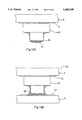
- FIG. 1 is a diagram showing a capillary for ball bonding in a first example according to the invention.
- FIG. 2A is a schematic cross-sectional view of an end portion of a capillary shown in FIG. 1.
- FIG. 2B is a diagram showing the shape of the end portion of the capillary in detail.
- FIG. 3 shows an exemplary bonder to which a capillary of the invention is attached.
- FIGs. 4A to 4E are diagrams schematically showing a method of forming two-stage bumps using the capillary of the invention.
- FIG. 5 is a diagram illustrating a process of pressing and shaping the bumps using the capillary of the invention.
- FIG. 6 shows a typical shape of a two-stage bump formed by a ball bonding method using the capillary of the first example.
- FIGs. 7A to 7C are diagrams showing possible shapes of a protrusion of the capillary of the invention.
- FIG. 8 is a diagram showing an example of a mounted semiconductor device (a semiconductor unit) with a two-stage bump formed according to the invention.
- FIGs. 9A and 9B illustrate a method for bonding a semiconductor device having a two-stage bump formed according to the invention onto a circuit board with conductive adhesive, and show a semiconductor unit after the bonding.
- FIGS. 10A and 10B show semiconductor units in which a semiconductor device having a two-stage bump formed according to the invention is electrically connected onto a circuit board with an anisotropic conductive member.
- FIG. 11 is a diagram showing a capillary for ball bonding in a second example according to the invention.
- FIG. 12A is a schematic cross-sectional view of an end portion of a capillary shown in FIG. 11.
- FIG. 12B is a diagram showing the shape of the end portion of the capillary in detail.
- FIG. 13 is a cross-sectional view of an end portion of a capillary for ball bonding in a third example according to the invention.
- FIG. 14 shows a shape of a two-stage bump formed using the capillary of the third example.
- FIGS. 15A and 15B illustrate a method for bonding a semiconductor device having a two-stage bump formed according to the invention onto a circuit board with conductive adhesive, and show a semiconductor unit obtained after the bonding.
- FIGs. 16A and 16B show semiconductor units in which a semiconductor device having a two-stage bump formed according to the invention is electrically connected onto a circuit board with an anisotropic conductive member.
- FIG. 17 is a cross-sectional view showing an end portion of a capillary for ball bonding in a fourth example according to the invention.
- FIG. 18A shows a two-stage bump formed by the capillary in the fourth example.
- FIG. 18B shows a shape of a two-stage bump with the tip portion thereof fallen.
- FIG. 19 is a diagram showing an exemplary conventional capillary for a wire bonding apparatus.
- FIG. 20A is a schematic cross-sectional view showing an end portion of the capillary shown in FIG. 19.
- FIG. 20B is a diagram showing the shape of the end portion of the capillary in detail.
- FIG. 21 is a diagram showing another exemplary conventional capillary for a wire bonding apparatus.
- FIG. 22A is a schematic cross-sectional view showing an end portion of the capillary shown in FIG. 21.
- FIG. 22B is a diagram showing the shape of the end portion of the capillary in detail.
- FIGS. 23A to 23D are diagrams schematically illustrating a method of forming a two-stage bump by a ball bonding method using a conventional capillary.
- FIG. 24 is a diagram showing a shape of a typical two-stage bump formed according to a conventional ball bonding method.
- FIG. 25 is a diagram illustrating a leveling process according to the conventional ball bonding method.
- FIG. 26 is a diagram showing a typical shape of a bump after the leveling process according to the conventional ball bonding method.
- FIGS. 27A to 27C show undesirable shapes of two-stage bumps formed according to the conventional ball bonding method.
- FIGs. 28A and 28B show shapes of defective bumps caused as the result of the conventional leveling process.
- FIG. 1 shows a capillary 1 for ball bonding in a first example according to the invention.
- FIG. 2A is a schematic cross-sectional view of an end portion 10 of the capillary 1.
- FIG. 2B shows in more detail the shape of the end portion 10 of the capillary 1.
- the cylindrical capillary 1 has a protrusion 3 as a leveling member provided on an outer circumference of the end portion 10.
- the capillary 1 is made of ceramic or artificial ruby.
- a bottom face 31 (a leveling plane) of the protrusion 3 is substantially parallel to the tip face 11 of the capillary 1.
- a height measured from the tip face 11 of the capillary 1 to the bottom face 31 is set to a predetermined value d.
- the area of the bottom face 31 can be selected depending on the bonding pitch and the diameter of the top end of the bump to be leveled.
- a bore 2 into which a metal wire for bonding is inserted.
- the diameter of the bore 2 is in the range of 25 ⁇ m to 50 ⁇ m.
- the end portion 10 of the capillary 1 has a cone shape with an angle ⁇ of about 10° to 30°, in view of the bonding pitch, and the shape and size of the metal wire (or a bump) after the bonding.
- FIG. 2B shows the shape of the end portion 10 of the capillary 1 when a metal wire having a diameter of about 25 ⁇ m is used.
- the bore diameter (hole diameter) H is 38 ⁇ m
- the tip diameter T is 203 ⁇ m
- the chamfer diameter CD is 74 ⁇ m.
- the above-described capillary 1 is, for example, attached to a bonder 500 shown in FIG. 3.
- the capillary 1 is attached to an end portion of an arm 510 which functions as an ultrasonic transmitting tool.
- a device (an IC chip) 501 to be subjected to the bonding is located on a bonding stage 520.
- the capillary 1 is moved upwards or downwards together with the arm 510.
- the device 501 is moved or rotated horizontally (in the X-Y direction) together with the bonding stage 520.
- the capillary 1 can be moved in a desirable direction and to a desirable position with respect to the device 501.
- FIGS. 4A to 4E schematically show a method of forming a two-stage bump 7 by a ball bonding method using the capillary 1 according to the invention, on an electrode pat 13 on an IC chip 6.
- a metal wire 4 having a diameter of 25 ⁇ m is inserted into a bore 2 of the capillary 1.
- Thermal energy is applied to the end of the metal wire 4 by gas flame, electric pulses, ultrasonic vibration, or the like.
- a ball 5 having a diameter which is about two or three times as large as the diameter of the metal wire 4 is formed at the end of the metal wire 4.
- the metal wire 4 can be made of a material to which the wire bonding method can be utilized, such as Au, Al, and Cu.
- the material and the diameter of the metal wire 4 can be selected depending on the outer diameter, the height, and the like of the bump 7 to be formed.
- the ball 5 formed at the end of the metal wire 4 is caused to abut against the electrode pad 13 of the IC chip 6 by moving the capillary 1 downwards.
- the ball 5 is secured to the electrode pad 13, so as to form a pedestal portion 9 of the bump 7 (the first bonding step).
- the first bonding is performed with the tip face 11 of the capillary 1.
- the pedestal portion 9 has an outer diameter of about 80 ⁇ m to 90 ⁇ m, and a height of about 20 ⁇ m to 30 ⁇ m.
- the capillary 1 is moved in a loop with respect to the IC chip 6. Specifically, the capillary 1 is first moved upwards above the pedestal portion 9 of the bump 7, and then moved in a loop. As is shown in FIG. 4D, by the loop movement of the capillary 1 with respect to the IC chip 6, a ring-shaped or reversed U-shaped portion of the metal wire 4 is formed on the pedestal portion 9. The portion constitutes a top portion 8 of the bump 7. The height of the top portion 8 in this step is about 40 ⁇ m to 50 ⁇ m.
- the capillary 1 is moved in such a manner that an edge 21 of the end portion of the capillary 1 is positioned at the outer circumference of the pedestal portion 9 of the bump 7, and then the capillary 1 is moved downwards so as to cut the metal wire 4 by the edge 21 (FIG. 4E).
- the capillary 1 is moved further downwards, as is shown in FIG. 5, so that the bump 7 is pressed and shaped by the bottom face 31 of the protrusion 3 which is provided on the outer circumference of the capillary 1 (the second bonding step).
- the capillary 1 is moved downwards until the tip face 11 abuts against the electrode pad 13.
- the total height of the bump 7 is set to be substantially equal to the height difference between the tip face 11 of the capillary 1 and the bottom face 31 of the protrusion 3 (i.e., the predetermined value d), thereby performing the leveling.
- the pressure for the first bonding can be set, for example, in the range of 25 g to 45 g per one bump, and the pressure for the second bonding can be set in the range of 70 g to 95 g per one bump.
- the pressures for bonding are adjusted depending on the material of the wire and the wire diameter.
- FIG. 6 shows the shape of a typical two-stage bump formed by the ball bonding method according to this example.
- the outer diameter R is about 80 ⁇ m to 90 ⁇ m
- the total height h 1 is about 40 ⁇ m to 50 ⁇ m
- the diameter r at the top 81 of the top portion 8 is about 40 ⁇ m to 50 ⁇ m
- the height h 2 of the pedestal portion 9 is about 15 ⁇ m to 25 ⁇ m.
- the leveling of the bump 7 can be performed in the process of forming the bump 7.
- the time required for this process is substantially the same as that required for forming only the bump 107 in the prior art example. Therefore, the corresponding time compared to the conventional leveling process can be saved.
- the capillary 1 presses the bump 7 until the tip face 11 thereof abuts against the electrode pad 13, so that the metal wire 4 which forms the tip portion 8 of the bump 7 can be cut more easily.
- one side of the bump 7 is supported by a side face of the end portion of the capillary 1 in the leveling, so that the falling down of the top portion which occurs in the leveling as shown in FIG. 28B can be prevented.
- the invention it is possible to prevent the formation of bumps having undesired shapes (defective bumps) which cannot be improved by the conventional leveling process. Also, the bumps can be formed so as to have substantially uniform shapes, so that it is possible to more surely connect the semiconductor device to the circuit board.
- the capillary 1 has a cylindrical shape
- the protrusion 3 also has a cylindrical shape so that the bottom face 31 is basically circular in view of the processibility for producing the capillary 1 (FIG. 7A). It is desirable that the bottom face 31 of the protrusion 3 be set parallel to the IC chip 6 in the leveling.
- any other shape of protrusion is available.
- a disk-like protrusion 3a shown in FIG. 7B can be used, and a protrusion 3b can be provided on one side of the capillary 1 as is shown in FIG. 7C.
- FIG. 8 shows a semiconductor unit 600 in which the semiconductor device having the bump 7 is mounted on a lead (terminal electrode) group 12 formed on a flexible resin film via the bump 7.
- the bump 7 is made of Au.
- the material of the lead group 12 may be a plating of Au or Sn having a foundation of Ni, or may be Al, Cu, or solder.
- the ultrasonic vibration can additionally be used.
- the compression bonding may be performed only by the ultrasonic vibration.
- the material of the lead group 12 may be a plating of Au or Sn having a foundation of Ni, or may be Al, Cu, or solder.
- FIGS. 9A and 9B illustrate a method for bonding the bump 7 of the semiconductor device onto the terminal electrode 12 of the circuit board 15 with conductive adhesive 14, and show a semiconductor unit 700 obtained after the bonding.
- the conductive adhesive 14 is applied to the top of the bump 7 of the semiconductor device by a transfer method or a printing method.
- the bump 7 having two-stage projected portions, an excess amount of conductive adhesive 14 is prevented from adhering to the bump 7.
- a suitable amount of conductive adhesive 14 can be applied to the bump 7.
- the semiconductor device is mounted facedown onto the circuit board 15.
- the conductive adhesive 14 is thermally cured at a temperature in the range of 80° C. to 150° C, so as to form an adhesion layer.
- the bump 7 of the semiconductor device is electrically connected to the terminal electrode 12 on the circuit board 15.
- the semiconductor device is mounted on the circuit board.
- the formation of defective bumps including the second peeling and tail standing can be prevented, and the conductive adhesive cannot be held and spread by the peeled portion or the tail portion. This means that there is little probability of a short-circuit with adjacent bumps or electrodes. Therefore, it is possible to connect the semiconductor device to the circuit board with high reliability.
- FIGS. 10A and 10B show a semiconductor unit in which the semiconductor device is electrically connected to the terminal electrode 12 of the circuit board 15 with an anisotropic conductive member.
- a thin anisotropic conductive member 16 is disposed on the terminal electrode 12 formed on the circuit board 15.
- the semiconductor device with the bump 7 is located facedown thereon.
- a portion of the anisotropic conductive member 16 sandwiched between the bump 7 and the terminal electrode 12 is thermo-compressed and bonded.
- the electric connection can be obtained.
- thermo-compressed portion of the anisotropic conductive member 16 conductive particles included in the anisotropic conductive member 16 are pressed by the bump 7, and bonded to each other. Also, the conductive particles are sunk into the surface of the terminal electrode 12, so that the bump 7 and the terminal electrode 12 are electrically connected to each other. In the remaining portion which are not compressed, the conductive particles exist separately from each other, so that the electric insulation is maintained.
- FIG. 10B shows a semiconductor unit 900 which utilizes an anisotropic conductive member 16' with a thickness larger than the total thickness of the bump 7 and the terminal electrode 12.
- the thick anisotropic conductive member 16' is disposed on the terminal electrode 12 formed on the circuit board 15.
- the semiconductor device with the bump 7 is located facedown thereon.
- a portion of the anisotropic conductive member 16' sandwiched between the bump 7 and the terminal electrode 12 is compressed.
- the electric connection can be obtained.
- only the portion sandwiched between the bump 7 and the terminal electrode 12 is compressed, and the remaining portion maintains the electric insulation.
- the remaining portion of the anisotropic conductive member 16' functions as insulating adhesive.
- the resin is thermally cured, the semiconductor is bonded to the circuit board.
- FIG. 11 shows a capillary 41 for ball bonding in a second example according to the invention.
- FIG. 12A is a schematic cross-sectional view of an end portion 40 of the capillary 41.
- FIG. 12B shows the shape of the end portion 40 of the capillary 41 in more detail.
- the capillary 41 is provided with a bottleneck 400 having a tapered end.
- the height of the bottleneck is generally about 500 ⁇ m. In FIG. 12A, the height is set to be 460 ⁇ m.
- the cylindrical capillary 41 has a protrusion 43 as a leveling member provided on an outer circumference of the bottleneck 400.
- the capillary 41 is made of ceramic or artificial ruby.
- the bottom face 431 (a leveling plane) of the protrusion 43 is substantially parallel to the tip face 411 of the capillary 41.
- the height measured from the tip face 411 of the capillary 41 to the bottom face 431 is set to a predetermined value d.
- a bore 2 into which a metal wire for bonding is inserted, the same as in the capillary 1.
- the diameter of the bore 2 is in the range of about 25 ⁇ m to 50 ⁇ m.
- the end portion of the capillary 41 (the bottleneck 400) has a cone shape with an angle of about 10°, in view of the bonding pitch, and the shape and size of the metal wire (or a bump) after the bonding.
- FIG. 12B shows the shape of the end portion of the capillary 41 when a metal wire having a diameter of about 25 ⁇ m is used.
- the bore diameter (hole diameter) H is 38 ⁇ m
- the tip diameter T is 152 ⁇ m
- the chamfer diameter CD is 64 ⁇ m.
- the above-described capillary 41 is, for example, attached to a bonder 500 shown in FIG. 3, the same as in the case of the capillary 1.
- the method of forming the two-stage bump 7 using the capillary 41 is the same as the method described in the first example.
- the formation and the leveling of the bump 7 can be performed in one and the same process even in the case of the finer bonding pitch, without adding another leveling process.
- the bumps can be formed to have uniform shapes, so that it is possible to more surely connect the semiconductor device to the circuit board.
- FIG. 13 is a cross-sectional view of the end portion of a capillary 51 for ball bonding in a third example of the invention.
- the cylindrical capillary 51 has a protrusion 53 provided on the outer circumference of the end portion thereof.
- a bottom face (a leveling plane) 531 of the protrusion 53 includes a rugged side 54.
- the term "rugged side” means a side having a surface which is roughened by forming a number of grooves of a width of 0.1 ⁇ m to 10 ⁇ m in various directions.
- the other portions of the capillary 51 can be formed in the same manner as in the capillary 1 or the capillary 41, depending on the required bonding pitch.
- the method of forming the two-stage bump using the capillary 51 is the same as that described in the first example.
- a rugged side 58 is formed at the top of the bump 57 by the rugged side 54 on the bottom face 531.
- the ultrasonic vibration is applied.
- the two-stage bump 57 formed using the capillary 51 is shown in FIG. 14.
- FIGS. 15A and 15B illustrate a method for bonding the bump 57 of the semiconductor device onto a terminal electrode 12 formed on a circuit board 15 with conductive adhesive 14, and show a semiconductor unit 710 obtained after the bonding.
- the adhering method is the same as that described in the first example with reference to FIGS. 10A and 10B.
- the bump 57 having a two-stage projecting shape By using the bump 57 having a two-stage projecting shape, an excess amount of conductive adhesive 14 is prevented from adhering to the bump 57. Thus, a suitable amount of conductive adhesive 14 can be applied to the bump 57.
- the rugged side 58 is formed at the top of the bump 57, the adhering area of the conductive adhesive 14 can be increased.
- conductive particles of the conductive adhesive 14 get into the grooves of the rugged side 58, so that the electric conductivity can be more surely attained. Therefore, a semiconductor unit with higher reliability can be obtained.
- FIGS. 16A and 16B show semiconductor units 810 and 910, respectively, in which the semiconductor device is electrically connected onto the terminal electrode 12 of the circuit board 15 with an anisotropic conductive member.
- the semiconductor units 810 and 910 are mounted in the same way as in the semiconductor units 800 and 900 described in the first example.
- the rugged side 58 is formed at the top of the bump 57, the surface area of the bump 57 which is in contact with the conductive particles is increased. Thus, a good electric contact can be attained.
- the formation of the rugged side 58 increased the surface area of the bump 57 in contact with the conductive particles of the anisotropic conductive member 16 or 16' and the adhering area of the resin. Accordingly, the conductivity and the adhesion strength are increased, so that an electric connection with higher reliability can be attained.
- each conductive particle in the anisotropic conductive member is in the range of about 1 ⁇ m to 10 ⁇ m. In order to effectively attain the electric contact, it is necessary to appropriately select the degree of roughness of the rugged side formed at the top of the bump and the size of the conductive particle.
- the rugged side 54 is provided over the entire bottom face 531 of the protrusion 53.
- the rugged side 54 may be provided in a desired portion of the bottom face 531.
- the capillary 51 has a cylindrical shape
- the protrusion 53 also has a cylindrical shape so that the bottom face 531 is basically circular in view of the processibility for producing the capillary 51.
- any other shape of protrusion is available as described in the first example.
- FIG. 17 is a cross-sectional view of the end portion of a capillary 61 for ball bonding in a fourth example of the invention.
- the cylindrical capillary 61 has a protrusion 63 provided on an outer circumference of the end portion.
- a bottom face 631 of the protrusion 63 includes a leveling plane 65 and a guiding portion 64.
- the leveling plane 65 of the protrusion 63 is substantially parallel to the tip face 611 of the capillary 61.
- the height measured from the tip face 611 of the capillary 61 to the leveling plane 65 is set to be predetermined value d.
- the value d of the height is set depending on the bump height to be formed.
- the guiding portion 64 is a portion projected vertically (downwards) and provided along the outer periphery of the bottom face 631.
- the guiding portion 64 holds a top portion 68 of the two-stage bump 67 in the second bonding (leveling), so as to prevent the top portion 68 of the two-stage bump 67 from falling down as is shown in FIG. 18B.
- the two-stage bump 67 formed using the capillary 61 is shown in FIG. 18A.
- the shape of the guiding portion 64 is not limited to any particular shape, as far as the two-stage bump 67 thus formed has a shape with which the bump 67 can keep a sufficient amount of the transferred conductive adhesive.
- the top portion 68 may be formed so that a side face of the top portion 68 is vertical.
- the other portions of the capillary 61 are the same as those in the capillary 1 or the capillary 41, depending on the desired bonding pitch.
- the method of forming the two-stage bump 67 using the capillary 61 is the same as the method described in the first example.
- the bump 67 is pressed and shaped by the leveling plane 65 of the bottom face 631 of the protrusion 63 provided on the outer circumference of the capillary 61 in the second bonding, and the top portion 68 of the bump 67 is supported by the guiding portion 64 formed along the outer periphery of the bottom face 631 in the second bonding. Accordingly, the falling down of the top portion 68 of the two-stage bump 67 can be prevented, and defective bumps such as those shown in FIGS. 28A and 28B which occur in the conventional leveling process can be prevented.
- the top portions 68 can have substantially equal areas.
- the guiding portion 64 is provided on the entire outer peripheral portion of the bottom face 631.
- the guiding portion 64 may be provided on a desired portion of the outer peripheral portion of the bottom face 631.
- the capillary 61 has a cylindrical shape
- the protrusion 63 also has a cylindrical shape so that the bottom face 631 is basically circular in view of the processibility for producing the capillary 61.
- the protrusion 63 is projected from the outer circumference of the capillary 61 and is provided with a leveling plane for leveling the bump 67 and a guiding portion for supporting the top portion 68 of the bump 67, any other shape of protrusion is available as described in the first example. It is desirable that the leveling plane 65 of the protrusion 63 be set parallel to the IC chip 6 in the leveling.
- the leveling of bumps can be performed in the formation process of the bumps of the semiconductor device, so that it is possible to obtain bumps with a desired height and a desired shape without adding another leveling process. Therefore, not only the time and cost required for adding another leveling process are saved, but it is possible to form leveled bumps for easily connecting the semiconductor device to a circuit board with high reliability. Furthermore, according to the invention, the formation of bumps having undesired shapes can be prevented, and it is possible to form bumps having uniform shapes with much reduced variation.
- the semiconductor device and the circuit board can be positively electrically connected and bonded to each other, so that it is possible to perform a stable and reliable mounting of the semiconductor device.
- the number of production processes and the production costs are both reduced, and the effects of the invention are equal to or greater than those of the prior art, so that the versatility for the practical use is extremely high.
Landscapes
- Engineering & Computer Science (AREA)
- Computer Hardware Design (AREA)
- Microelectronics & Electronic Packaging (AREA)
- Power Engineering (AREA)
- Manufacturing & Machinery (AREA)
- Mechanical Engineering (AREA)
- Wire Bonding (AREA)
Abstract
Description
Claims (19)
Applications Claiming Priority (4)
Application Number | Priority Date | Filing Date | Title |
---|---|---|---|
JP5-103848 | 1993-04-30 | ||
JP10384893 | 1993-04-30 | ||
JP13709093 | 1993-06-08 | ||
JP5-137090 | 1993-06-08 |
Publications (1)
Publication Number | Publication Date |
---|---|
US5485949A true US5485949A (en) | 1996-01-23 |
Family
ID=26444443
Family Applications (1)
Application Number | Title | Priority Date | Filing Date |
---|---|---|---|
US08/233,829 Expired - Fee Related US5485949A (en) | 1993-04-30 | 1994-04-26 | Capillary for a wire bonding apparatus and a method for forming an electric connection bump using the capillary |
Country Status (5)
Country | Link |
---|---|
US (1) | US5485949A (en) |
EP (1) | EP0622149B1 (en) |
KR (1) | KR0137909B1 (en) |
CN (1) | CN1031907C (en) |
DE (1) | DE69401233T2 (en) |
Cited By (94)
Publication number | Priority date | Publication date | Assignee | Title |
---|---|---|---|---|
US5908317A (en) * | 1996-03-11 | 1999-06-01 | Anam Semiconductor Inc. | Method of forming chip bumps of bump chip scale semiconductor package |
US5954260A (en) * | 1996-12-17 | 1999-09-21 | Texas Instruments Incorporated | Fine pitch bonding technique |
EP0954208A1 (en) * | 1996-12-27 | 1999-11-03 | Matsushita Electric Industrial Co., Ltd. | Method and device for mounting electronic component on circuit board |
US5981371A (en) * | 1996-03-15 | 1999-11-09 | Kabushiki Kaisha Shinkawa | Bump forming method |
US6012625A (en) * | 1995-03-10 | 2000-01-11 | Fraunhofer-Gesellschaft Zur Forderungder Angewandten Forschung E.V. | Process and device for forming raised metallised contacts |
US6041996A (en) * | 1996-11-22 | 2000-03-28 | Matsushita Electric Industrial Co., Ltd. | Method of pressure bonding a bumped electronic part and an apparatus for pressure bonding a bumped electronic part |
US6079610A (en) * | 1996-10-07 | 2000-06-27 | Denso Corporation | Wire bonding method |
US6155474A (en) * | 1997-12-16 | 2000-12-05 | Texas Instruments Incorporated | Fine pitch bonding technique |
US6158647A (en) * | 1998-09-29 | 2000-12-12 | Micron Technology, Inc. | Concave face wire bond capillary |
US6207549B1 (en) * | 1996-10-01 | 2001-03-27 | Matsushita Electric Industrial Co., Ltd. | Method of forming a ball bond using a bonding capillary |
US6244499B1 (en) * | 1999-12-13 | 2001-06-12 | Advanced Semiconductor Engineering, Inc. | Structure of a ball bump for wire bonding and the formation thereof |
US6260753B1 (en) * | 1998-08-07 | 2001-07-17 | Stmicroelectronics S.R.L. | Gold bumps bonding on connection pads and subsequent coining of their vertex |
US20010053598A1 (en) * | 1998-11-13 | 2001-12-20 | Seiko Epson Corporation | Semiconductor device having bumps |
US20020018591A1 (en) * | 1999-12-16 | 2002-02-14 | Kei Murayama | Bump inspection apparatus and method |
US6350632B1 (en) | 2000-09-20 | 2002-02-26 | Charles W. C. Lin | Semiconductor chip assembly with ball bond connection joint |
US6350386B1 (en) | 2000-09-20 | 2002-02-26 | Charles W. C. Lin | Method of making a support circuit with a tapered through-hole for a semiconductor chip assembly |
US20020072214A1 (en) * | 1998-10-28 | 2002-06-13 | Seiko Epson Corporation | Semiconductor device and method of fabrication thereof, circuit board, and electronic equipment |
US6440835B1 (en) | 2000-10-13 | 2002-08-27 | Charles W. C. Lin | Method of connecting a conductive trace to a semiconductor chip |
US6444489B1 (en) | 2000-12-15 | 2002-09-03 | Charles W. C. Lin | Semiconductor chip assembly with bumped molded substrate |
US6448108B1 (en) | 2000-10-02 | 2002-09-10 | Charles W. C. Lin | Method of making a semiconductor chip assembly with a conductive trace subtractively formed before and after chip attachment |
US6454159B1 (en) * | 1999-08-18 | 2002-09-24 | International Business Machines Corporation | Method for forming electrical connecting structure |
US20020158374A1 (en) * | 2001-02-28 | 2002-10-31 | Billiet Romain L. | Ultrasmall semiconductor bonding tools and method of fabrication thereof |
US6492252B1 (en) | 2000-10-13 | 2002-12-10 | Bridge Semiconductor Corporation | Method of connecting a bumped conductive trace to a semiconductor chip |
US20020185735A1 (en) * | 1998-10-28 | 2002-12-12 | International Business Machines Corporation | Bump connection and method and apparatus for forming said connection |
US6511865B1 (en) | 2000-09-20 | 2003-01-28 | Charles W. C. Lin | Method for forming a ball bond connection joint on a conductive trace and conductive pad in a semiconductor chip assembly |
US6537851B1 (en) | 2000-10-13 | 2003-03-25 | Bridge Semiconductor Corporation | Method of connecting a bumped compliant conductive trace to a semiconductor chip |
US6544813B1 (en) | 2000-10-02 | 2003-04-08 | Charles W. C. Lin | Method of making a semiconductor chip assembly with a conductive trace subtractively formed before and after chip attachment |
US6548393B1 (en) | 2000-10-13 | 2003-04-15 | Charles W. C. Lin | Semiconductor chip assembly with hardened connection joint |
US6576493B1 (en) | 2000-10-13 | 2003-06-10 | Bridge Semiconductor Corporation | Method of connecting a conductive trace and an insulative base to a semiconductor chip using multiple etch steps |
US6576539B1 (en) | 2000-10-13 | 2003-06-10 | Charles W.C. Lin | Semiconductor chip assembly with interlocked conductive trace |
US6581816B2 (en) * | 2000-04-11 | 2003-06-24 | Stmicroelectronics S.R.L. | Capillary for bonding copper wires between a semiconductor circuit chip and a corresponding terminal connector of a semiconductor device |
US6583040B1 (en) | 2000-10-13 | 2003-06-24 | Bridge Semiconductor Corporation | Method of making a pillar in a laminated structure for a semiconductor chip assembly |
US6601752B2 (en) | 2000-03-13 | 2003-08-05 | Denso Corporation | Electronic part mounting method |
US6622903B1 (en) * | 2002-03-27 | 2003-09-23 | Palomar Technologies, Inc. | Production of a tailless ball bump |
US6653170B1 (en) | 2001-02-06 | 2003-11-25 | Charles W. C. Lin | Semiconductor chip assembly with elongated wire ball bonded to chip and electrolessly plated to support circuit |
US6667229B1 (en) | 2000-10-13 | 2003-12-23 | Bridge Semiconductor Corporation | Method of connecting a bumped compliant conductive trace and an insulative base to a semiconductor chip |
US20040026480A1 (en) * | 2002-08-08 | 2004-02-12 | Kaijo Corporation | Wire bonding method, method of forming bump and bump |
US6699780B1 (en) | 2000-10-13 | 2004-03-02 | Bridge Semiconductor Corporation | Method of connecting a conductive trace to a semiconductor chip using plasma undercut etching |
US6740576B1 (en) | 2000-10-13 | 2004-05-25 | Bridge Semiconductor Corporation | Method of making a contact terminal with a plated metal peripheral sidewall portion for a semiconductor chip assembly |
US20040152292A1 (en) * | 2002-09-19 | 2004-08-05 | Stephen Babinetz | Method and apparatus for forming bumps for semiconductor interconnections using a wire bonding machine |
US20040164127A1 (en) * | 2003-02-17 | 2004-08-26 | Kabushiki Kaisha Shinkawa | Wire bonding method |
US20040178481A1 (en) * | 2003-03-10 | 2004-09-16 | Rajeev Joshi | Dual metal stud bumping for flip chip applications |
US20050042855A1 (en) * | 2003-03-24 | 2005-02-24 | Kazuaki Ano | Wire bonding for thin semiconductor package |
US6872591B1 (en) | 2000-10-13 | 2005-03-29 | Bridge Semiconductor Corporation | Method of making a semiconductor chip assembly with a conductive trace and a substrate |
US6876072B1 (en) | 2000-10-13 | 2005-04-05 | Bridge Semiconductor Corporation | Semiconductor chip assembly with chip in substrate cavity |
US20050092815A1 (en) * | 2003-10-30 | 2005-05-05 | Kabushiki Kaisha Shinkawa | Semiconductor device and wire bonding method |
US6908788B1 (en) | 2000-10-13 | 2005-06-21 | Bridge Semiconductor Corporation | Method of connecting a conductive trace to a semiconductor chip using a metal base |
US6949408B1 (en) | 2000-10-13 | 2005-09-27 | Bridge Semiconductor Corporation | Method of connecting a conductive trace and an insulative base to a semiconductor chip using multiple etch steps |
US6984576B1 (en) | 2000-10-13 | 2006-01-10 | Bridge Semiconductor Corporation | Method of connecting an additively and subtractively formed conductive trace and an insulative base to a semiconductor chip |
US20060014316A1 (en) * | 2000-10-13 | 2006-01-19 | Bridge Semiconductor Corporation | Method of making a semiconductor chip assemby with a metal containment wall and a solder terminal |
US7009297B1 (en) | 2000-10-13 | 2006-03-07 | Bridge Semiconductor Corporation | Semiconductor chip assembly with embedded metal particle |
US20060125112A1 (en) * | 2004-11-19 | 2006-06-15 | Yukihiro Ikeya | Apparatus and method for manufacturing semiconductor device |
US7071089B1 (en) | 2000-10-13 | 2006-07-04 | Bridge Semiconductor Corporation | Method of making a semiconductor chip assembly with a carved bumped terminal |
US7075186B1 (en) | 2000-10-13 | 2006-07-11 | Bridge Semiconductor Corporation | Semiconductor chip assembly with interlocked contact terminal |
US7094676B1 (en) | 2000-10-13 | 2006-08-22 | Bridge Semiconductor Corporation | Semiconductor chip assembly with embedded metal pillar |
US7112521B1 (en) | 2000-10-13 | 2006-09-26 | Bridge Semiconductor Corporation | Method of making a semiconductor chip assembly with a bumped metal pillar |
US20060237856A1 (en) * | 1993-11-16 | 2006-10-26 | Formfactor, Inc. | Microelectronic Contact Structure And Method Of Making Same |
US7129113B1 (en) | 2000-10-13 | 2006-10-31 | Bridge Semiconductor Corporation | Method of making a three-dimensional stacked semiconductor package with a metal pillar in an encapsulant aperture |
US7132741B1 (en) | 2000-10-13 | 2006-11-07 | Bridge Semiconductor Corporation | Semiconductor chip assembly with carved bumped terminal |
US20060262961A1 (en) * | 2000-06-14 | 2006-11-23 | Troy Holsing Et Al. | System and method for image based sensor calibration |
US7190080B1 (en) | 2000-10-13 | 2007-03-13 | Bridge Semiconductor Corporation | Semiconductor chip assembly with embedded metal pillar |
US20070119903A1 (en) * | 2005-11-28 | 2007-05-31 | Lee Jung K | Two-step high bottleneck type capillary for wire bonding device |
US7262082B1 (en) | 2000-10-13 | 2007-08-28 | Bridge Semiconductor Corporation | Method of making a three-dimensional stacked semiconductor package with a metal pillar and a conductive interconnect in an encapsulant aperture |
US7264991B1 (en) | 2000-10-13 | 2007-09-04 | Bridge Semiconductor Corporation | Method of connecting a conductive trace to a semiconductor chip using conductive adhesive |
US7268421B1 (en) | 2004-11-10 | 2007-09-11 | Bridge Semiconductor Corporation | Semiconductor chip assembly with welded metal pillar that includes enlarged ball bond |
US7319265B1 (en) | 2000-10-13 | 2008-01-15 | Bridge Semiconductor Corporation | Semiconductor chip assembly with precision-formed metal pillar |
US7396703B1 (en) | 2003-11-20 | 2008-07-08 | Bridge Semiconductor Corporation | Method of making a semiconductor chip assembly with a bumped terminal and a filler |
US7446419B1 (en) | 2004-11-10 | 2008-11-04 | Bridge Semiconductor Corporation | Semiconductor chip assembly with welded metal pillar of stacked metal balls |
US7494843B1 (en) | 2006-12-26 | 2009-02-24 | Bridge Semiconductor Corporation | Method of making a semiconductor chip assembly with thermal conductor and encapsulant grinding |
US7538415B1 (en) | 2003-11-20 | 2009-05-26 | Bridge Semiconductor Corporation | Semiconductor chip assembly with bumped terminal, filler and insulative base |
US20100093229A1 (en) * | 1996-02-21 | 2010-04-15 | Formfactor, Inc. | Microelectronic contact structure and method of making same |
US7750483B1 (en) | 2004-11-10 | 2010-07-06 | Bridge Semiconductor Corporation | Semiconductor chip assembly with welded metal pillar and enlarged plated contact terminal |
US20100186991A1 (en) * | 2006-10-18 | 2010-07-29 | Kulicke And Soffa Industries, Inc. | conductive bumps, wire loops including the improved conductive bumps, and methods of forming the same |
US20100206940A1 (en) * | 2008-09-10 | 2010-08-19 | Kaijo Corporation | Wire bonding method, wire bonding apparatus, and wire bonding control program |
US7811863B1 (en) | 2006-10-26 | 2010-10-12 | Bridge Semiconductor Corporation | Method of making a semiconductor chip assembly with metal pillar and encapsulant grinding and heat sink attachment |
US7993983B1 (en) | 2003-11-17 | 2011-08-09 | Bridge Semiconductor Corporation | Method of making a semiconductor chip assembly with chip and encapsulant grinding |
US20130119117A1 (en) * | 2011-11-04 | 2013-05-16 | Invensas Corporation | Bonding wedge |
USD753739S1 (en) | 2015-04-17 | 2016-04-12 | Coorstek, Inc. | Wire bonding wedge tool |
US20160284619A1 (en) * | 2006-11-10 | 2016-09-29 | STATS ChipPAC Pte. Ltd. | Semiconductor Package with Embedded Die |
USD771168S1 (en) | 2014-10-31 | 2016-11-08 | Coorstek, Inc. | Wire bonding ceramic capillary |
USD797172S1 (en) | 2015-02-03 | 2017-09-12 | Coorstek, Inc. | Ceramic bonding tool with textured tip |
USD797171S1 (en) | 2015-02-03 | 2017-09-12 | Coorstek, Inc. | Ceramic bonding tool with textured tip |
USD797826S1 (en) | 2015-02-03 | 2017-09-19 | Coorstek, Inc. | Ceramic bonding tool with textured tip |
US9833818B2 (en) | 2004-09-28 | 2017-12-05 | International Test Solutions, Inc. | Working surface cleaning system and method |
US10361169B2 (en) | 2017-04-24 | 2019-07-23 | International Test Solutions, Inc. | Semiconductor wire bonding machine cleaning device and method |
USD868123S1 (en) | 2016-12-20 | 2019-11-26 | Coorstek, Inc. | Wire bonding wedge tool |
US10717618B2 (en) | 2018-02-23 | 2020-07-21 | International Test Solutions, Inc. | Material and hardware to automatically clean flexible electronic web rolls |
US10792713B1 (en) | 2019-07-02 | 2020-10-06 | International Test Solutions, Inc. | Pick and place machine cleaning system and method |
US20210111146A1 (en) * | 2019-10-10 | 2021-04-15 | Skyworks Solutions, Inc. | Cupd wire bond capillary design |
US11035898B1 (en) | 2020-05-11 | 2021-06-15 | International Test Solutions, Inc. | Device and method for thermal stabilization of probe elements using a heat conducting wafer |
US11211242B2 (en) | 2019-11-14 | 2021-12-28 | International Test Solutions, Llc | System and method for cleaning contact elements and support hardware using functionalized surface microfeatures |
US11217558B2 (en) | 2017-06-29 | 2022-01-04 | PAC Tech—Packaging Technologies GmbH | Method and device for establishing a wire connection as well as a component arrangement having a wire connection |
US11318550B2 (en) | 2019-11-14 | 2022-05-03 | International Test Solutions, Llc | System and method for cleaning wire bonding machines using functionalized surface microfeatures |
US11756811B2 (en) | 2019-07-02 | 2023-09-12 | International Test Solutions, Llc | Pick and place machine cleaning system and method |
Families Citing this family (7)
Publication number | Priority date | Publication date | Assignee | Title |
---|---|---|---|---|
US5544804A (en) * | 1994-06-08 | 1996-08-13 | Texas Instruments Incorporated | Capillary designs and process for fine pitch ball bonding |
CN1201383C (en) | 1999-01-29 | 2005-05-11 | 松下电器产业株式会社 | Electronic parts mounting method and device therefor |
US6321969B1 (en) * | 2000-04-28 | 2001-11-27 | Kulicke & Soffa Investments | Efficient energy transfer capillary |
US6910612B2 (en) | 2001-07-17 | 2005-06-28 | Kulicke & Soffa Investments, Inc. | Capillary with contained inner chamfer |
US6715658B2 (en) | 2001-07-17 | 2004-04-06 | Kulicke & Soffa Investments, Inc. | Ultra fine pitch capillary |
JP4057457B2 (en) * | 2003-04-15 | 2008-03-05 | 株式会社ディスコ | Flip chip bonder |
CN102549730B (en) * | 2009-09-30 | 2015-02-11 | Toto株式会社 | Bonding capillary |
Citations (8)
Publication number | Priority date | Publication date | Assignee | Title |
---|---|---|---|---|
JPS54128271A (en) * | 1978-03-29 | 1979-10-04 | Hitachi Ltd | Capillary of wire bonder |
US4415115A (en) * | 1981-06-08 | 1983-11-15 | Motorola, Inc. | Bonding means and method |
JPS59130435A (en) * | 1983-09-21 | 1984-07-27 | Hitachi Ltd | Wedge for supersonic wire bonder |
JPH0196938A (en) * | 1987-10-09 | 1989-04-14 | Sanken Electric Co Ltd | Capillary for wire bonding |
EP0320244A2 (en) * | 1987-12-08 | 1989-06-14 | Matsushita Electric Industrial Co., Ltd. | Electrical contact bump and a package provided with the same |
JPH0250328A (en) * | 1988-08-12 | 1990-02-20 | Pioneer Electron Corp | Optical information recording medium and player thereof |
US5172851A (en) * | 1990-09-20 | 1992-12-22 | Matsushita Electronics Corporation | Method of forming a bump electrode and manufacturing a resin-encapsulated semiconductor device |
US5364004A (en) * | 1993-05-10 | 1994-11-15 | Hughes Aircraft Company | Wedge bump bonding apparatus and method |
-
1994
- 1994-04-26 US US08/233,829 patent/US5485949A/en not_active Expired - Fee Related
- 1994-04-27 EP EP19940106580 patent/EP0622149B1/en not_active Expired - Lifetime
- 1994-04-27 DE DE69401233T patent/DE69401233T2/en not_active Expired - Fee Related
- 1994-04-29 CN CN94106952A patent/CN1031907C/en not_active Expired - Fee Related
- 1994-04-30 KR KR1019940009401A patent/KR0137909B1/en not_active IP Right Cessation
Patent Citations (8)
Publication number | Priority date | Publication date | Assignee | Title |
---|---|---|---|---|
JPS54128271A (en) * | 1978-03-29 | 1979-10-04 | Hitachi Ltd | Capillary of wire bonder |
US4415115A (en) * | 1981-06-08 | 1983-11-15 | Motorola, Inc. | Bonding means and method |
JPS59130435A (en) * | 1983-09-21 | 1984-07-27 | Hitachi Ltd | Wedge for supersonic wire bonder |
JPH0196938A (en) * | 1987-10-09 | 1989-04-14 | Sanken Electric Co Ltd | Capillary for wire bonding |
EP0320244A2 (en) * | 1987-12-08 | 1989-06-14 | Matsushita Electric Industrial Co., Ltd. | Electrical contact bump and a package provided with the same |
JPH0250328A (en) * | 1988-08-12 | 1990-02-20 | Pioneer Electron Corp | Optical information recording medium and player thereof |
US5172851A (en) * | 1990-09-20 | 1992-12-22 | Matsushita Electronics Corporation | Method of forming a bump electrode and manufacturing a resin-encapsulated semiconductor device |
US5364004A (en) * | 1993-05-10 | 1994-11-15 | Hughes Aircraft Company | Wedge bump bonding apparatus and method |
Non-Patent Citations (5)
Title |
---|
"High Density I/O Pad Wire Ball Bonding Capillary Tool," (1987) May No. 277; 2244 Research Disclosure. |
"Tab Bumping Technique", (1992) Apr., No. 336, 2244 Research Disclosure. |
High Density I/O Pad Wire Ball Bonding Capillary Tool, (1987) May No. 277; 2244 Research Disclosure. * |
Search Report for European Appl. 94106580.7, mailed Aug. 22, 1994. * |
Tab Bumping Technique , (1992) Apr., No. 336, 2244 Research Disclosure. * |
Cited By (157)
Publication number | Priority date | Publication date | Assignee | Title |
---|---|---|---|---|
US20060237856A1 (en) * | 1993-11-16 | 2006-10-26 | Formfactor, Inc. | Microelectronic Contact Structure And Method Of Making Same |
US6012625A (en) * | 1995-03-10 | 2000-01-11 | Fraunhofer-Gesellschaft Zur Forderungder Angewandten Forschung E.V. | Process and device for forming raised metallised contacts |
US8033838B2 (en) | 1996-02-21 | 2011-10-11 | Formfactor, Inc. | Microelectronic contact structure |
US20100093229A1 (en) * | 1996-02-21 | 2010-04-15 | Formfactor, Inc. | Microelectronic contact structure and method of making same |
US5908317A (en) * | 1996-03-11 | 1999-06-01 | Anam Semiconductor Inc. | Method of forming chip bumps of bump chip scale semiconductor package |
US5981371A (en) * | 1996-03-15 | 1999-11-09 | Kabushiki Kaisha Shinkawa | Bump forming method |
US7071090B2 (en) | 1996-10-01 | 2006-07-04 | Matsushita Electric Industrial Co., Ltd. | Semiconductor element having protruded bump electrodes |
US20050146029A1 (en) * | 1996-10-01 | 2005-07-07 | Kazushi Higashi | Semiconductor element having protruded bump electrodes |
US6894387B2 (en) | 1996-10-01 | 2005-05-17 | Matsushita Electric Industrial Co., Ltd. | Semiconductor element having protruded bump electrodes |
US6207549B1 (en) * | 1996-10-01 | 2001-03-27 | Matsushita Electric Industrial Co., Ltd. | Method of forming a ball bond using a bonding capillary |
US6079610A (en) * | 1996-10-07 | 2000-06-27 | Denso Corporation | Wire bonding method |
US6041996A (en) * | 1996-11-22 | 2000-03-28 | Matsushita Electric Industrial Co., Ltd. | Method of pressure bonding a bumped electronic part and an apparatus for pressure bonding a bumped electronic part |
US5954260A (en) * | 1996-12-17 | 1999-09-21 | Texas Instruments Incorporated | Fine pitch bonding technique |
EP1448034A1 (en) * | 1996-12-27 | 2004-08-18 | Matsushita Electric Industrial Co., Ltd. | Method and device for mounting electronic component on circuit board |
EP1448033A1 (en) * | 1996-12-27 | 2004-08-18 | Matsushita Electric Industrial Co., Ltd. | Method and device for mounting electronic component on a circuit board |
EP1445995A1 (en) * | 1996-12-27 | 2004-08-11 | Matsushita Electric Industrial Co., Ltd. | Method of mounting an electronic component on a circuit board |
US6981317B1 (en) | 1996-12-27 | 2006-01-03 | Matsushita Electric Industrial Co., Ltd. | Method and device for mounting electronic component on circuit board |
EP0954208A4 (en) * | 1996-12-27 | 2002-09-11 | Matsushita Electric Ind Co Ltd | Method and device for mounting electronic component on circuit board |
EP0954208A1 (en) * | 1996-12-27 | 1999-11-03 | Matsushita Electric Industrial Co., Ltd. | Method and device for mounting electronic component on circuit board |
US6155474A (en) * | 1997-12-16 | 2000-12-05 | Texas Instruments Incorporated | Fine pitch bonding technique |
US6260753B1 (en) * | 1998-08-07 | 2001-07-17 | Stmicroelectronics S.R.L. | Gold bumps bonding on connection pads and subsequent coining of their vertex |
US6311890B1 (en) | 1998-09-29 | 2001-11-06 | Micron Technology, Inc. | Concave face wire bond capillary |
US20040056072A1 (en) * | 1998-09-29 | 2004-03-25 | Chapman Gregory M. | Concave face wire bond capillary and method |
US6966480B2 (en) | 1998-09-29 | 2005-11-22 | Micron Technology, Inc. | Concave face wire bond capillary and method |
US6158647A (en) * | 1998-09-29 | 2000-12-12 | Micron Technology, Inc. | Concave face wire bond capillary |
US6439450B1 (en) | 1998-09-29 | 2002-08-27 | Micron Technology, Inc. | Concave face wire bond capillary |
US6595406B2 (en) | 1998-09-29 | 2003-07-22 | Micron Technology, Inc. | Concave face wire bond capillary and method |
US7677429B2 (en) | 1998-09-29 | 2010-03-16 | Micron Technology, Inc. | Concave face wire bond capillary and method |
US20080302862A1 (en) * | 1998-09-29 | 2008-12-11 | Micron Technology, Inc. | Concave face wire bond capillary and method |
US20060032888A1 (en) * | 1998-09-29 | 2006-02-16 | Chapman Gregory M | Concave face wire bond capillary and method |
US7416107B2 (en) | 1998-09-29 | 2008-08-26 | Micron Technology, Inc. | Concave face wire bond capillary and method |
US6551918B2 (en) * | 1998-10-28 | 2003-04-22 | Seiko Epson Corporation | Semiconductor device and method of fabrication thereof, circuit board, and electronic equipment |
US7021521B2 (en) * | 1998-10-28 | 2006-04-04 | International Business Machines Corporation | Bump connection and method and apparatus for forming said connection |
US20020072214A1 (en) * | 1998-10-28 | 2002-06-13 | Seiko Epson Corporation | Semiconductor device and method of fabrication thereof, circuit board, and electronic equipment |
US20020185735A1 (en) * | 1998-10-28 | 2002-12-12 | International Business Machines Corporation | Bump connection and method and apparatus for forming said connection |
US6689679B2 (en) * | 1998-11-13 | 2004-02-10 | Seiko Epson Corporation | Semiconductor device having bumps |
US20010053598A1 (en) * | 1998-11-13 | 2001-12-20 | Seiko Epson Corporation | Semiconductor device having bumps |
US6454159B1 (en) * | 1999-08-18 | 2002-09-24 | International Business Machines Corporation | Method for forming electrical connecting structure |
US6244499B1 (en) * | 1999-12-13 | 2001-06-12 | Advanced Semiconductor Engineering, Inc. | Structure of a ball bump for wire bonding and the formation thereof |
US20020018591A1 (en) * | 1999-12-16 | 2002-02-14 | Kei Murayama | Bump inspection apparatus and method |
US6601752B2 (en) | 2000-03-13 | 2003-08-05 | Denso Corporation | Electronic part mounting method |
US6581816B2 (en) * | 2000-04-11 | 2003-06-24 | Stmicroelectronics S.R.L. | Capillary for bonding copper wires between a semiconductor circuit chip and a corresponding terminal connector of a semiconductor device |
US20060262961A1 (en) * | 2000-06-14 | 2006-11-23 | Troy Holsing Et Al. | System and method for image based sensor calibration |
US6350632B1 (en) | 2000-09-20 | 2002-02-26 | Charles W. C. Lin | Semiconductor chip assembly with ball bond connection joint |
US6627824B1 (en) | 2000-09-20 | 2003-09-30 | Charles W. C. Lin | Support circuit with a tapered through-hole for a semiconductor chip assembly |
US6350386B1 (en) | 2000-09-20 | 2002-02-26 | Charles W. C. Lin | Method of making a support circuit with a tapered through-hole for a semiconductor chip assembly |
US6511865B1 (en) | 2000-09-20 | 2003-01-28 | Charles W. C. Lin | Method for forming a ball bond connection joint on a conductive trace and conductive pad in a semiconductor chip assembly |
US6448108B1 (en) | 2000-10-02 | 2002-09-10 | Charles W. C. Lin | Method of making a semiconductor chip assembly with a conductive trace subtractively formed before and after chip attachment |
US6544813B1 (en) | 2000-10-02 | 2003-04-08 | Charles W. C. Lin | Method of making a semiconductor chip assembly with a conductive trace subtractively formed before and after chip attachment |
US6740576B1 (en) | 2000-10-13 | 2004-05-25 | Bridge Semiconductor Corporation | Method of making a contact terminal with a plated metal peripheral sidewall portion for a semiconductor chip assembly |
US7015128B1 (en) | 2000-10-13 | 2006-03-21 | Bridge Semiconductor Corporation | Method of making a semiconductor chip assembly with an embedded metal particle |
US7319265B1 (en) | 2000-10-13 | 2008-01-15 | Bridge Semiconductor Corporation | Semiconductor chip assembly with precision-formed metal pillar |
US7414319B2 (en) | 2000-10-13 | 2008-08-19 | Bridge Semiconductor Corporation | Semiconductor chip assembly with metal containment wall and solder terminal |
US6699780B1 (en) | 2000-10-13 | 2004-03-02 | Bridge Semiconductor Corporation | Method of connecting a conductive trace to a semiconductor chip using plasma undercut etching |
US7264991B1 (en) | 2000-10-13 | 2007-09-04 | Bridge Semiconductor Corporation | Method of connecting a conductive trace to a semiconductor chip using conductive adhesive |
US6673710B1 (en) | 2000-10-13 | 2004-01-06 | Bridge Semiconductor Corporation | Method of connecting a conductive trace and an insulative base to a semiconductor chip |
US6667229B1 (en) | 2000-10-13 | 2003-12-23 | Bridge Semiconductor Corporation | Method of connecting a bumped compliant conductive trace and an insulative base to a semiconductor chip |
US6653217B1 (en) | 2000-10-13 | 2003-11-25 | Charles W. C. Lin | Method of connecting a conductive trace to a semiconductor chip |
US6800506B1 (en) | 2000-10-13 | 2004-10-05 | Bridge Semiconductor Corporation | Method of making a bumped terminal in a laminated structure for a semiconductor chip assembly |
US6809414B1 (en) | 2000-10-13 | 2004-10-26 | Bridge Semiconductor Corporation | Semiconductor chip assembly with bumped conductive trace |
US7262082B1 (en) | 2000-10-13 | 2007-08-28 | Bridge Semiconductor Corporation | Method of making a three-dimensional stacked semiconductor package with a metal pillar and a conductive interconnect in an encapsulant aperture |
US6872591B1 (en) | 2000-10-13 | 2005-03-29 | Bridge Semiconductor Corporation | Method of making a semiconductor chip assembly with a conductive trace and a substrate |
US6876072B1 (en) | 2000-10-13 | 2005-04-05 | Bridge Semiconductor Corporation | Semiconductor chip assembly with chip in substrate cavity |
US7232706B1 (en) | 2000-10-13 | 2007-06-19 | Bridge Semiconductor Corporation | Method of making a semiconductor chip assembly with a precision-formed metal pillar |
US6653742B1 (en) | 2000-10-13 | 2003-11-25 | Charles W. C. Lin | Semiconductor chip assembly with interlocked conductive trace |
US6908788B1 (en) | 2000-10-13 | 2005-06-21 | Bridge Semiconductor Corporation | Method of connecting a conductive trace to a semiconductor chip using a metal base |
US7232707B1 (en) | 2000-10-13 | 2007-06-19 | Bridge Semiconductor Corporation | Method of making a semiconductor chip assembly with an interlocked contact terminal |
US6949408B1 (en) | 2000-10-13 | 2005-09-27 | Bridge Semiconductor Corporation | Method of connecting a conductive trace and an insulative base to a semiconductor chip using multiple etch steps |
US6608374B1 (en) | 2000-10-13 | 2003-08-19 | Bridge Semiconductor Corporation | Semiconductor chip assembly with bumped conductive trace |
US6440835B1 (en) | 2000-10-13 | 2002-08-27 | Charles W. C. Lin | Method of connecting a conductive trace to a semiconductor chip |
US6583040B1 (en) | 2000-10-13 | 2003-06-24 | Bridge Semiconductor Corporation | Method of making a pillar in a laminated structure for a semiconductor chip assembly |
US6984576B1 (en) | 2000-10-13 | 2006-01-10 | Bridge Semiconductor Corporation | Method of connecting an additively and subtractively formed conductive trace and an insulative base to a semiconductor chip |
US20060014316A1 (en) * | 2000-10-13 | 2006-01-19 | Bridge Semiconductor Corporation | Method of making a semiconductor chip assemby with a metal containment wall and a solder terminal |
US20060012024A1 (en) * | 2000-10-13 | 2006-01-19 | Bridge Semiconductor Corporation | Semiconductor chip assembly with metal containment wall and solder terminal |
US6576539B1 (en) | 2000-10-13 | 2003-06-10 | Charles W.C. Lin | Semiconductor chip assembly with interlocked conductive trace |
US7009297B1 (en) | 2000-10-13 | 2006-03-07 | Bridge Semiconductor Corporation | Semiconductor chip assembly with embedded metal particle |
US7419851B2 (en) | 2000-10-13 | 2008-09-02 | Bridge Semiconductor Corporation | Method of making a semiconductor chip assembly with a metal containment wall and a solder terminal |
US6576493B1 (en) | 2000-10-13 | 2003-06-10 | Bridge Semiconductor Corporation | Method of connecting a conductive trace and an insulative base to a semiconductor chip using multiple etch steps |
US6548393B1 (en) | 2000-10-13 | 2003-04-15 | Charles W. C. Lin | Semiconductor chip assembly with hardened connection joint |
US6537851B1 (en) | 2000-10-13 | 2003-03-25 | Bridge Semiconductor Corporation | Method of connecting a bumped compliant conductive trace to a semiconductor chip |
US7067911B1 (en) | 2000-10-13 | 2006-06-27 | Bridge Semiconductor Corporation | Three-dimensional stacked semiconductor package with metal pillar in encapsulant aperture |
US7071573B1 (en) | 2000-10-13 | 2006-07-04 | Bridge Semiconductor Corporation | Semiconductor chip assembly with welded metal pillar |
US6492252B1 (en) | 2000-10-13 | 2002-12-10 | Bridge Semiconductor Corporation | Method of connecting a bumped conductive trace to a semiconductor chip |
US7071089B1 (en) | 2000-10-13 | 2006-07-04 | Bridge Semiconductor Corporation | Method of making a semiconductor chip assembly with a carved bumped terminal |
US7075186B1 (en) | 2000-10-13 | 2006-07-11 | Bridge Semiconductor Corporation | Semiconductor chip assembly with interlocked contact terminal |
US7190080B1 (en) | 2000-10-13 | 2007-03-13 | Bridge Semiconductor Corporation | Semiconductor chip assembly with embedded metal pillar |
US7094676B1 (en) | 2000-10-13 | 2006-08-22 | Bridge Semiconductor Corporation | Semiconductor chip assembly with embedded metal pillar |
US7112521B1 (en) | 2000-10-13 | 2006-09-26 | Bridge Semiconductor Corporation | Method of making a semiconductor chip assembly with a bumped metal pillar |
US7132741B1 (en) | 2000-10-13 | 2006-11-07 | Bridge Semiconductor Corporation | Semiconductor chip assembly with carved bumped terminal |
US7129113B1 (en) | 2000-10-13 | 2006-10-31 | Bridge Semiconductor Corporation | Method of making a three-dimensional stacked semiconductor package with a metal pillar in an encapsulant aperture |
US7129575B1 (en) | 2000-10-13 | 2006-10-31 | Bridge Semiconductor Corporation | Semiconductor chip assembly with bumped metal pillar |
US6444489B1 (en) | 2000-12-15 | 2002-09-03 | Charles W. C. Lin | Semiconductor chip assembly with bumped molded substrate |
US6653170B1 (en) | 2001-02-06 | 2003-11-25 | Charles W. C. Lin | Semiconductor chip assembly with elongated wire ball bonded to chip and electrolessly plated to support circuit |
US20020158374A1 (en) * | 2001-02-28 | 2002-10-31 | Billiet Romain L. | Ultrasmall semiconductor bonding tools and method of fabrication thereof |
US7083757B2 (en) * | 2001-02-28 | 2006-08-01 | Billiet Romain L | Method of making semiconductor bonding tools |
US6622903B1 (en) * | 2002-03-27 | 2003-09-23 | Palomar Technologies, Inc. | Production of a tailless ball bump |
US6715666B2 (en) * | 2002-08-08 | 2004-04-06 | Kaijo Corporation | Wire bonding method, method of forming bump and bump |
KR100533487B1 (en) * | 2002-08-08 | 2005-12-05 | 가부시끼가이샤가이죠 | Wire bonding method, method of forming bump and bump |
US20040026480A1 (en) * | 2002-08-08 | 2004-02-12 | Kaijo Corporation | Wire bonding method, method of forming bump and bump |
US7229906B2 (en) * | 2002-09-19 | 2007-06-12 | Kulicke And Soffa Industries, Inc. | Method and apparatus for forming bumps for semiconductor interconnections using a wire bonding machine |
US7651022B2 (en) * | 2002-09-19 | 2010-01-26 | Kulicke And Soffa Industries, Inc. | Method and apparatus for forming bumps for semiconductor interconnections using a wire bonding machine |
US20070199974A1 (en) * | 2002-09-19 | 2007-08-30 | Kulicke And Soffa Industries, Inc. | Method and apparatus for forming bumps for semiconductor interconnections using a wire bonding machine |
US20040152292A1 (en) * | 2002-09-19 | 2004-08-05 | Stephen Babinetz | Method and apparatus for forming bumps for semiconductor interconnections using a wire bonding machine |
US7025247B2 (en) * | 2003-02-17 | 2006-04-11 | Kabushiki Kaisha Shinkawa | Wire bonding method |
US20040164127A1 (en) * | 2003-02-17 | 2004-08-26 | Kabushiki Kaisha Shinkawa | Wire bonding method |
US7932171B2 (en) | 2003-03-10 | 2011-04-26 | Fairchild Semiconductor Corporation | Dual metal stud bumping for flip chip applications |
US20040178481A1 (en) * | 2003-03-10 | 2004-09-16 | Rajeev Joshi | Dual metal stud bumping for flip chip applications |
US7271497B2 (en) | 2003-03-10 | 2007-09-18 | Fairchild Semiconductor Corporation | Dual metal stud bumping for flip chip applications |
US20090186452A1 (en) * | 2003-03-10 | 2009-07-23 | Rajeev Joshi | Dual metal stud bumping for flip chip applications |
US20050042855A1 (en) * | 2003-03-24 | 2005-02-24 | Kazuaki Ano | Wire bonding for thin semiconductor package |
US7192861B2 (en) * | 2003-03-24 | 2007-03-20 | Texas Instruments Incorporated | Wire bonding for thin semiconductor package |
US20050092815A1 (en) * | 2003-10-30 | 2005-05-05 | Kabushiki Kaisha Shinkawa | Semiconductor device and wire bonding method |
US7993983B1 (en) | 2003-11-17 | 2011-08-09 | Bridge Semiconductor Corporation | Method of making a semiconductor chip assembly with chip and encapsulant grinding |
US7453140B1 (en) | 2003-11-20 | 2008-11-18 | Bridge Semiconductor Corporation | Semiconductor chip assembly with laterally aligned filler and insulative base |
US7932165B1 (en) | 2003-11-20 | 2011-04-26 | Bridge Semiconductor Corporation | Method of making a semiconductor chip assembly with a laterally aligned filler and insulative base |
US7459385B1 (en) | 2003-11-20 | 2008-12-02 | Bridge Semiconductor Corporation | Method of making a semiconductor chip assembly with a laterally aligned bumped terminal and filler |
US7538415B1 (en) | 2003-11-20 | 2009-05-26 | Bridge Semiconductor Corporation | Semiconductor chip assembly with bumped terminal, filler and insulative base |
US7833827B1 (en) | 2003-11-20 | 2010-11-16 | Bridge Semiconductor Corporation | Method of making a semiconductor chip assembly with a bumped terminal, a filler and an insulative base |
US7425759B1 (en) | 2003-11-20 | 2008-09-16 | Bridge Semiconductor Corporation | Semiconductor chip assembly with bumped terminal and filler |
US7417314B1 (en) | 2003-11-20 | 2008-08-26 | Bridge Semiconductor Corporation | Semiconductor chip assembly with laterally aligned bumped terminal and filler |
US7396703B1 (en) | 2003-11-20 | 2008-07-08 | Bridge Semiconductor Corporation | Method of making a semiconductor chip assembly with a bumped terminal and a filler |
US10406568B2 (en) | 2004-09-28 | 2019-09-10 | International Test Solutions, Inc. | Working surface cleaning system and method |
US10239099B2 (en) | 2004-09-28 | 2019-03-26 | International Test Solutions, Inc. | Working surface cleaning system and method |
US9833818B2 (en) | 2004-09-28 | 2017-12-05 | International Test Solutions, Inc. | Working surface cleaning system and method |
US7268421B1 (en) | 2004-11-10 | 2007-09-11 | Bridge Semiconductor Corporation | Semiconductor chip assembly with welded metal pillar that includes enlarged ball bond |
US7750483B1 (en) | 2004-11-10 | 2010-07-06 | Bridge Semiconductor Corporation | Semiconductor chip assembly with welded metal pillar and enlarged plated contact terminal |
US7446419B1 (en) | 2004-11-10 | 2008-11-04 | Bridge Semiconductor Corporation | Semiconductor chip assembly with welded metal pillar of stacked metal balls |
US20060125112A1 (en) * | 2004-11-19 | 2006-06-15 | Yukihiro Ikeya | Apparatus and method for manufacturing semiconductor device |
US20070119903A1 (en) * | 2005-11-28 | 2007-05-31 | Lee Jung K | Two-step high bottleneck type capillary for wire bonding device |
US20100186991A1 (en) * | 2006-10-18 | 2010-07-29 | Kulicke And Soffa Industries, Inc. | conductive bumps, wire loops including the improved conductive bumps, and methods of forming the same |
US7811863B1 (en) | 2006-10-26 | 2010-10-12 | Bridge Semiconductor Corporation | Method of making a semiconductor chip assembly with metal pillar and encapsulant grinding and heat sink attachment |
US20160284619A1 (en) * | 2006-11-10 | 2016-09-29 | STATS ChipPAC Pte. Ltd. | Semiconductor Package with Embedded Die |
US7494843B1 (en) | 2006-12-26 | 2009-02-24 | Bridge Semiconductor Corporation | Method of making a semiconductor chip assembly with thermal conductor and encapsulant grinding |
US8042725B2 (en) * | 2008-09-10 | 2011-10-25 | Kaijo Corporation | Wire bonding method, wire bonding apparatus, and wire bonding control program |
US20100206940A1 (en) * | 2008-09-10 | 2010-08-19 | Kaijo Corporation | Wire bonding method, wire bonding apparatus, and wire bonding control program |
US20130119117A1 (en) * | 2011-11-04 | 2013-05-16 | Invensas Corporation | Bonding wedge |
USD771168S1 (en) | 2014-10-31 | 2016-11-08 | Coorstek, Inc. | Wire bonding ceramic capillary |
USD821468S1 (en) | 2015-02-03 | 2018-06-26 | Coorstek, Inc. | Ceramic bonding tool with textured tip |
USD797826S1 (en) | 2015-02-03 | 2017-09-19 | Coorstek, Inc. | Ceramic bonding tool with textured tip |
USD824970S1 (en) | 2015-02-03 | 2018-08-07 | Coorstek, Inc. | Ceramic bonding tool with textured tip |
USD824969S1 (en) | 2015-02-03 | 2018-08-07 | Coorstek, Inc. | Ceramic bonding tool with textured tip |
USD797171S1 (en) | 2015-02-03 | 2017-09-12 | Coorstek, Inc. | Ceramic bonding tool with textured tip |
USD797172S1 (en) | 2015-02-03 | 2017-09-12 | Coorstek, Inc. | Ceramic bonding tool with textured tip |
USD753739S1 (en) | 2015-04-17 | 2016-04-12 | Coorstek, Inc. | Wire bonding wedge tool |
USD868123S1 (en) | 2016-12-20 | 2019-11-26 | Coorstek, Inc. | Wire bonding wedge tool |
US10361169B2 (en) | 2017-04-24 | 2019-07-23 | International Test Solutions, Inc. | Semiconductor wire bonding machine cleaning device and method |
US11217558B2 (en) | 2017-06-29 | 2022-01-04 | PAC Tech—Packaging Technologies GmbH | Method and device for establishing a wire connection as well as a component arrangement having a wire connection |
US10717618B2 (en) | 2018-02-23 | 2020-07-21 | International Test Solutions, Inc. | Material and hardware to automatically clean flexible electronic web rolls |
US10843885B2 (en) | 2018-02-23 | 2020-11-24 | International Test Solutions, Inc. | Material and hardware to automatically clean flexible electronic web rolls |
US11155428B2 (en) | 2018-02-23 | 2021-10-26 | International Test Solutions, Llc | Material and hardware to automatically clean flexible electronic web rolls |
US11434095B2 (en) | 2018-02-23 | 2022-09-06 | International Test Solutions, Llc | Material and hardware to automatically clean flexible electronic web rolls |
US10792713B1 (en) | 2019-07-02 | 2020-10-06 | International Test Solutions, Inc. | Pick and place machine cleaning system and method |
US11756811B2 (en) | 2019-07-02 | 2023-09-12 | International Test Solutions, Llc | Pick and place machine cleaning system and method |
US20210111146A1 (en) * | 2019-10-10 | 2021-04-15 | Skyworks Solutions, Inc. | Cupd wire bond capillary design |
US11211242B2 (en) | 2019-11-14 | 2021-12-28 | International Test Solutions, Llc | System and method for cleaning contact elements and support hardware using functionalized surface microfeatures |
US11318550B2 (en) | 2019-11-14 | 2022-05-03 | International Test Solutions, Llc | System and method for cleaning wire bonding machines using functionalized surface microfeatures |
US11035898B1 (en) | 2020-05-11 | 2021-06-15 | International Test Solutions, Inc. | Device and method for thermal stabilization of probe elements using a heat conducting wafer |
Also Published As
Publication number | Publication date |
---|---|
EP0622149A1 (en) | 1994-11-02 |
DE69401233D1 (en) | 1997-02-06 |
KR0137909B1 (en) | 1998-06-01 |
EP0622149B1 (en) | 1996-12-27 |
DE69401233T2 (en) | 1997-06-26 |
CN1098819A (en) | 1995-02-15 |
CN1031907C (en) | 1996-05-29 |
Similar Documents
Publication | Publication Date | Title |
---|---|---|
US5485949A (en) | Capillary for a wire bonding apparatus and a method for forming an electric connection bump using the capillary | |
US5090119A (en) | Method of forming an electrical contact bump | |
US5545589A (en) | Method of forming a bump having a rugged side, a semiconductor device having the bump, and a method of mounting a semiconductor unit and a semiconductor device | |
US5786271A (en) | Production of semiconductor package having semiconductor chip mounted with its face down on substrate with protruded electrodes therebetween and semiconductor package | |
US7759240B2 (en) | Use of palladium in IC manufacturing with conductive polymer bump | |
US5650667A (en) | Process of forming conductive bumps on the electrodes of semiconductor chips using lapping and the bumps thereby created | |
US20050221535A1 (en) | Method for making self-coplanarity bumping shape for flip chip | |
KR100201036B1 (en) | Bump, semiconductor chip and package having the bump, and mounting method and semiconductor apparatus | |
US6420787B1 (en) | Semiconductor device and process of producing same | |
US5877079A (en) | Method for manufacturing a semiconductor device and a method for mounting a semiconductor device for eliminating a void | |
US6396155B1 (en) | Semiconductor device and method of producing the same | |
US6528889B1 (en) | Electronic circuit device having adhesion-reinforcing pattern on a circuit board for flip-chip mounting an IC chip | |
US5854558A (en) | Test board for testing a semiconductor device and method of testing the semiconductor device | |
JP2951882B2 (en) | Semiconductor device manufacturing method and semiconductor device manufactured using the same | |
JPH07142488A (en) | Bump structure, formation thereof and flip-chip mounting structure | |
JPH063820B2 (en) | Semiconductor device mounting method | |
US6489180B1 (en) | Flip-chip packaging process utilizing no-flow underfill technique | |
JP3022151B2 (en) | Capillary for wire bonding apparatus and method for forming electrical connection bump using the capillary | |
JPH09162230A (en) | Electronic circuit device and its manufacturing method | |
JP2943788B2 (en) | Wiring board for mounting electronic components | |
JP3370842B2 (en) | Semiconductor device mounting structure | |
KR100192758B1 (en) | Method of manufacturing semiconductor package and structure of the same | |
JP2002118210A (en) | Interposer for semiconductor device and semiconductor using the same | |
JPH08186117A (en) | Method for capillary and bump forming of wire bonding apparatus | |
JP2000252320A (en) | Semiconductor device and manufacture thereof |
Legal Events
Date | Code | Title | Description |
---|---|---|---|
AS | Assignment |
Owner name: MATSUSHITA ELECTRIC INDUSTRIAL CO., LTD. 1006, OH Free format text: ASSIGNMENT OF ASSIGNORS INTEREST;ASSIGNORS:TOMURA, Y.;BESSHO, Y.;REEL/FRAME:007087/0006 Effective date: 19940606 |
|
FEPP | Fee payment procedure |
Free format text: PAYOR NUMBER ASSIGNED (ORIGINAL EVENT CODE: ASPN); ENTITY STATUS OF PATENT OWNER: LARGE ENTITY |
|
FPAY | Fee payment |
Year of fee payment: 4 |
|
FPAY | Fee payment |
Year of fee payment: 8 |
|
REMI | Maintenance fee reminder mailed | ||
LAPS | Lapse for failure to pay maintenance fees | ||
STCH | Information on status: patent discontinuation |
Free format text: PATENT EXPIRED DUE TO NONPAYMENT OF MAINTENANCE FEES UNDER 37 CFR 1.362 |
|
FP | Lapsed due to failure to pay maintenance fee |
Effective date: 20080123 |