US5459749A - Multi-level superposed amplitude-modulated baseband signal processor - Google Patents
Multi-level superposed amplitude-modulated baseband signal processor Download PDFInfo
- Publication number
- US5459749A US5459749A US08/172,198 US17219893A US5459749A US 5459749 A US5459749 A US 5459749A US 17219893 A US17219893 A US 17219893A US 5459749 A US5459749 A US 5459749A
- Authority
- US
- United States
- Prior art keywords
- signal
- output
- symbol
- level
- amplitude
- Prior art date
- Legal status (The legal status is an assumption and is not a legal conclusion. Google has not performed a legal analysis and makes no representation as to the accuracy of the status listed.)
- Expired - Lifetime
Links
Images


Classifications
-
- H—ELECTRICITY
- H04—ELECTRIC COMMUNICATION TECHNIQUE
- H04L—TRANSMISSION OF DIGITAL INFORMATION, e.g. TELEGRAPHIC COMMUNICATION
- H04L27/00—Modulated-carrier systems
- H04L27/02—Amplitude-modulated carrier systems, e.g. using on-off keying; Single sideband or vestigial sideband modulation
- H04L27/04—Modulator circuits; Transmitter circuits
-
- H—ELECTRICITY
- H04—ELECTRIC COMMUNICATION TECHNIQUE
- H04L—TRANSMISSION OF DIGITAL INFORMATION, e.g. TELEGRAPHIC COMMUNICATION
- H04L27/00—Modulated-carrier systems
- H04L27/32—Carrier systems characterised by combinations of two or more of the types covered by groups H04L27/02, H04L27/10, H04L27/18 or H04L27/26
- H04L27/34—Amplitude- and phase-modulated carrier systems, e.g. quadrature-amplitude modulated carrier systems
- H04L27/36—Modulator circuits; Transmitter circuits
- H04L27/362—Modulation using more than one carrier, e.g. with quadrature carriers, separately amplitude modulated
Definitions
- the present invention relates to a digital data transmission system which can be applied to such communication systems as satellite, ground-based network, mobile and cable communications, and more particularly, to a multi-level superposed amplitude-modulated baseband signal processor which receives a non-return-to-zero (NRZ) data stream and generates an output having a narrow frequency bandwidth and small side lobes even in a non-linear channel.
- NRZ non-return-to-zero
- digital communication methods As compared with existing analog communication methods, digital communication methods have high reliability and enable the transmission of high-quality information. Therefore, digital communication methods are forming the mainstream in modern information communication, and the use thereof has gradually been increasing.
- the carrier wave parameters for example, phase and amplitude, are modulated and transmitted in accordance with the information data to be transmitted. Then, the transmitted parameters are demodulated in the receiving portion, to thereby restore the data.
- the modulator's performance is evaluated by the characteristics of bandwidth efficiency and electrical power efficiency.
- the bandwidth is wide. Therefore, in general, the input data is modulated and transmitted after limiting the bandwidth through filtering or other means.
- good bandwidth efficiency can be obtained by gathering and transmitting a number of input data bits at one time in a single symbol unit selected among the symbols of a modulation signal. That is, a single symbol is formed by the input data being divided into bit groups consisting of k bits.
- the data consisting of k bits is modulated so that the amplitude or degree of phase change is in proportion to 2 k , which is the number of cases which k-bit data can express, a large amount of data can be transmitted even without extending the bandwidth on the power density spectrum.
- the reason for this is that the bandwidth is proportional to the symbol transmission speed, i.e., the reciprocal of the data symbol cycle, and remains unaffected by changes in amplitude or phase. This is called multi-level modulation.
- the present invention aims to obtain a bandwidth-efficient modulation signal in a digital transmission system, and more particularly, to provide the function of generating a filtered and multi-level modulated baseband signal.
- phase-shift-keying PSK
- PAM pulse amplitude modulation
- quadrature phase-shift-keying a modulation method wherein two signals by the BPSK modulation are disposed to be divided into an in-phase and a quadrature-phase on the signal space, is called quadrature phase-shift-keying (QPSK).
- QPSK quadrature phase-shift-keying
- the bandwidth on the power density spectrum occupied by the QPSK signal is half that of the BPSK signal.
- the QPSK method can transmit twice the information of the BPSK method, in the same bandwidth.
- a bandwidth-efficient modulation method for example, 8-PSK or 16-PSK, is introduced.
- a symbol point for representing the multi-level amplitude of input symbols as described above is located on the signal space. Then, multi-level quadrature amplitude modulation (QAM) signal is obtained by corresponding the symbol point to the multiple-bit input data.
- QAM quadrature amplitude modulation
- the information transmitted by a single symbol in a single signal space increases as the degree of the multi-level becomes higher, which results in a more bandwidth-efficient modulation method.
- the modulation signal occupies a very wide bandwidth. Therefore, before transmission, the bandwidth of the modulation signal is limited to maintain high performance.
- jitter i.e., a time difference generated when the signal passes the zero level
- the bandwidth is limited, thereby causing difficulties in restoring the timing of the symbol in a demodulator.
- Signals generated by the above patents produce two pulse shapes which correspond to a single bit of the input data stream, which is a NRZ-shaped binary code.
- the signals of the produced pulse shapes that is, a double-interval raised-cosine pulse and a common raised-cosine pulse, are superposed according to the ratio of the superposition (signal "A ⁇ of FIG. 1) and then output via an output terminal.
- a superposed modulation baseband signal is generated, which minimizes amplitude fluctuation.
- the superposed modulation signal where the superposed modulation baseband signal is used that is, the modulated carrier obtained using the above superposed modulation baseband signal is amplified via a non-linear amplifier and transmitted via a communication channel. Therefore, a bandwidth-efficient and power-efficient modulation signal can be obtained while the inter-symbol interference (ISI) between the jitter and the code of the transmitting terminal does not occur.
- ISI inter-symbol interference
- the main lobe bandwidth and the side lobe amplitude in power density spectrum can be controlled by controlling the superposition (A), which means that a suitably controlled bandwidth for a digital transmission system is possible. Also, when the superposition (A) equals one, the modulated output signal is identical to that of the invention by Dr. K. Feher.
- the devices of the inventions of the two patents for generating the superposed amplitude-modulated baseband signal use a non-linear method for obtaining the filtered and modulated signal. That is, devices of the inventions of the two patents generate a multitude of bandwidth-limited pulse waveforms corresponding to an output signal of the superposed amplitude-modulated baseband signal. Then, the pulse waveform selected among the pulse waveforms generated according to the pattern of the input data is output, to obtain a filtered and modulated signal.
- the inventions of the above patents generate a modulated signal from a single stream of input data, and are not multi-level amplitude modulation methods.
- a n is the amplitude of the multi-level signal space expressed by the input data to a point in time n, and corresponds to one element of the group consisting of ⁇ 1, ⁇ 3, ⁇ 5, . . ., ⁇ ( ⁇ M-1), when the superposition number is M.
- s(t) is a baseband signal impulse response to the basic superposed amplitude-modulated signal, which is expressed as follows. ##EQU2## where A is a superposed degree and T s is a symbol duration.
- the element that constitutes the baseband waveform when the superposed amplitude modulation signal is multi-level superposed amplitude-modulated is generated within the processor. Then, one selected from the pulse waveforms generated according to the input data form is output.
- All of the conventional multi-level superposed amplitude-modulated baseband signal generating methods generate a superposed amplitude-modulated signal which has a predetermined number of multi-levels. Therefore, when the number of multi-levels is required to be changed for flexibility of transmission systems, some of the generated pulse waveforms have to be included or omitted according to the change.
- a multi-level amplitude-modulated baseband signal processor having:
- data delaying means for receiving in parallel k-bit data constituting one symbol, and for delaying the k-bit data for one symbol cycle to output one-symbol-delayed data;
- signal level converting means for respectively receiving the k-bit data and the one-symbol-delayed data, converting the respectively received data into amplitude values selected among an amplitude set whose size is 2 k in the space of the multi-level superposed amplitude modulation signal expressed by the symbol, and outputting the resultant amplitude value;
- sgn(x) means sign of x
- means absolute value of y during the relevant single symbol cycle, given that the output of the signal level converting means is S3 and the output of the data delaying means is S4;
- a first pulse generator which repeatedly generates a cosine wave signal which is synchronized with the basic symbol clock of the input data stream and shaped as cos ⁇ ( ⁇ t)/T ⁇ , for the symbol cycle period (T);
- first selecting means for respectively receiving the output signal of the first pulse generator and the inversion of the output signal of the first pulse generator and selecting between the respectively received output signals in accordance with the output signal C from the operating device;
- a first amplifier for amplifying the first selected signal from the first selecting means, whose gain is controlled by the output signal B from the operating device;
- a first adder which sums the output signal of the first amplifier and the output signal D, and outputs the result
- a second pulse generator which repeatedly generates a cosine wave signal which is synchronized with the basic symbol clock of the input data stream and shaped as 0.5(1-A)(1-cos ⁇ (2 ⁇ t)/T ⁇ ), for the symbol cycle period (T) according to the degree (A) of superposition;
- second selecting means for respectively receiving the output signal of the second pulse generator and the inversion of the output signal of the second pulse generator and selecting between the respectively received output signals in accordance with the output signal F from the operating device;
- a second amplifier for amplifying the second selected signal from the second selecting means, whose gain is controlled by the output signal F from the operating device;
- a second adder which sums the outputs of the first adder and the second amplifier, thereby resulting in the output signal according to the present invention.
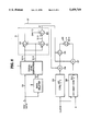
- FIG. 1 is a block diagram showing the structure of a multi-level superposed amplitude-modulated baseband signal processor according to the present invention
- FIG. 2 is a linear graphical representation for the operation of the processor shown in FIG. 1 wherein four amplitudes are expressed by one symbol (given that the number of multi-levels is four) and disposed in the signal space;
- FIG. 3 is a table for explaining the case where the number of the multi-levels is four, showing the operation of the processor shown in FIGS. 1 and 6;
- FIG. 4 is an eye pattern diagram representing the multi-level superposed amplitude-modulated baseband signal output of the processor shown in FIG. 1, when the number of the multi-levels is four and the degree of superposition is 0.8;
- FIG. 5 is a power spectrum diagram of the multi-level superposed amplitude-modulated baseband signal output from the processor shown in FIG. 1, when the number of the multi-levels is four and the degree of superposition is 0.8;
- FIG. 6 is a block diagram showing a multi-level superposed amplitude-modulated baseband signal processor according to an embodiment of the present invention.
- FIG. 7 is a linear graphical representation of the operation of the processor shown in FIG. 6 wherein four amplitudes and space numbers are expressed by one symbol (given that the number of multi-levels is four) and disposed in the signal space.
- FIG. 1 is a structural diagram of multi-level superposed amplitude-modulated baseband signal processor according to the present invention.
- the processor includes a signal level converter 1, a data delayer 2, an operating device 3, a first pulse generator 4, a first inverter 5, a first selector 6, a first amplifier 7, a first adder 8, a second pulse generator 9, a second inverter 10, a second selector 11, a second amplifier 12 and a second adder 13.
- NRZ data S1 to be transmitted consists of k bits and is connected to the input of signal level converter 1 and to the input of data delayer 2.
- the data stream input to data delayer 2 is delayed for one symbol cycle and then, after being converted into a delay signal S2, is connected to another input of signal level converter 1.
- the two groups of data S1 and S2 input to signal level converter 1 are respectively converted into the corresponding amplitude values S3 and S4 in the signal space to be output.
- the two output values S3 and S4 are respectively connected to the two inputs of the operating device 3.
- output signal B is connected to the gain control terminal of first amplifier 7
- output signal C is connected to the control terminal of the first selector 6
- output signal D is connected to an input of first adder 8
- output signal E is connected to the gain control terminal of the second amplifier 12
- output signal F is connected to a control terminal of the second selector 11.
- an input data basic symbol clock S5 is divided into two paths, where one is connected to the input of first pulse generator 4 and the other is connected to an input of second pulse generator 9.
- First and second pulse generators 4 and 9 respectively generate the cosine waveform pulses cos ⁇ ( ⁇ t)/T ⁇ and 0.5(1-A)(1-cos ⁇ (2 ⁇ t)/T ⁇ ) which are synchronized with symbol clock S5.
- These processors can be structured by the use of either a memory element or a bandpass filter.
- the former is a method for outputting the desired signal as one which is synchronized with a symbol clock output from a memory for storing the sample values calculated by the above expressions
- the latter is a method for outputting the desired signal by extracting elements of the symbol signal via bandpass-filtering.
- Output signal S6 is again divided into two paths, where one is connected to an input of first selector 6 and another is inverted via first inverter 5 and connected to the other input of first selector 6.
- First selector 6 selects and outputs either of the two input signals according to the C signal provided by operating device 3. The selected output signal is then supplied to the input of first amplifier 7.
- First amplifier 7 amplifies the input signal according to output signal B, which is a gain control voltage provided by operating device 3.
- the amplified input signal is supplied to an input of first adder 8.
- First adder 8 sums the output of first amplifier 7 and the output signal D provided by operating device 3 and provides the result to an input of second adder 13.
- output signal S8 of second pulse generator 9 is divided into two paths, of which one side is connected to an input of second selector 11 and another side is inverted by second inverter 10 and connected to another input of second selector 11.
- Second selector 11 selects either of the two input signals depending on the output signal F provided by operating device 3, and the output signal is provided to the input of second amplifier 12.
- Second amplifier 12 amplifies the input signal depending on the output signal E, i.e., a gain control voltage, provided by operating device 3, and the amplified output signal is supplied to the other input of second adder 13.
- Second adder 13 sums the outputs of second amplifier 12 and first adder 8, and outputs the final output signal S10 of the present invention.
- the case of generating the baseband signal required for a four-level (2-bit) superposed modulation signal is explained as an example.
- the two bits are input as the NRZ data S1 during one symbol cycle, and the multi-level amplitude-modulated baseband signals corresponding to the four symbols in the signal space are output.
- first selector 6 when the value of the output signal C from operating device 3 is greater than zero, first selector 6 is designed to select and output the output signal S7 of first inverter 5, and otherwise (C ⁇ 0), to select and output the output signal S6 of first pulse generator 4.
- second selector 11 when the value of the output signal F from operating device 3 is greater than zero, second selector 11 is designed to select and output the output signal S9 of second inverter 10, and otherwise (F ⁇ 0), to select and output the output signal S8 of second pulse generator 9.
- the gain factors of first and second amplifiers 7 and 12 are designed to correspond to the voltage values of signals B and E, respectively. Accordingly, if the values of the output signals B and E are one and three respectively, then first and second amplifiers 7 and 12 amplify the input signals by factors one and three, respectively.
- FIG. 2 illustrates the operation of the device shown in FIG. 1.
- the four amplitudes are disposed in the signal space when the number of the multi-levels (M) is 4.
- M multi-levels
- FIG. 3 shows waveforms for each part of the device according to the present invention, where the input NRZ data stream is input in the order of 00, 01, 00, 00, 11, 10, 10, 01, 11, 00, 01.
- the NRZ data S1 input by two bits per symbol period and the delayed data S2 in which the NRZ data is delayed for one symbol cycle by data delayer 2 are input to signal level converter 1. Then, signal level converter 1 outputs the signals S3 and S4 which are converted to the signal levels required for operating device 3.
- the levels of signals S3 and S4 are equal to the amplitudes corresponding to the NRZ data in the signal space.
- the output signal S4 is identical to the output signal S3 for the previous symbol cycle.
- the output signals S3 and S4 are provided to operating device 3 and operated as the following expressions (3) through (7). As a result, the control signal and voltage required for each part of the present invention can be obtained. ##EQU4##
- first selector 6 receives the output signal C as a control signal, and selects -cos ⁇ ( ⁇ t)/T ⁇ , i.e., output signal S7 of first inverter 5 (per the above assumption), since the value of the C signal is greater than zero.
- the selected -cos ⁇ ( ⁇ t)/T ⁇ is output to first amplifier 7.
- first amplifier 7 since the value of the output signal B, which is a gain control signal, is one, the input signal is amplified by a factor of one, which means that the input signal is directly transmitted to first adder 8.
- first adder 8 the output signal of first amplifier 7 and the output signal D provided by operating device 3 are summed.
- the summed result is the signal S7 shifted to a voltage value of negative two.
- second selector 11 receives the output signal F as a control signal.
- output signal S8 which is expressed as 0.5(1-A)(1-cos ⁇ (2 ⁇ t)/T ⁇ ), is selected and output to second amplifier 12 (per the above assumption).
- output signal E which is a gain control signal
- the input signal is amplified by a factor of four and transmitted to second adder 13.
- the output signal of first adder 8 which is the summation of the output signal of first amplifier 7 and the control signal D is supplied to a positive port, while a negative port of the second adder receives the output of second amplifier 12.
- the two inputs are summed such that the output of second amplifier is subtracted from the output signal of first adder, and then the four-level superposed amplitude-modulated baseband signal, i.e., S10 of the present invention, is output.
- the four-level superposed amplitude-modulated baseband signal shown as S10 of FIG. 3, is output for the following symbol cycles by the same operation as above.
- the amplitude level of the multi-level superposed amplitude-modulated baseband output signal generates one among 2 k amplitude levels, to enable the simple generation of the multi-level superposed amplitude-modulated baseband signal at the desired level.
- the signal generated by the present invention is employed instead of the output signal of bandwidth limitation filter which exists in the in-phase channel and the quadrature phase channel of the offset quadrature amplitude modulation (OQAM) method processor.
- OQAM offset quadrature amplitude modulation
- 16-SQAM 16-level superposed quadrature amplitude modulation
- FIG. 4 is an eye pattern diagram of the four-level superposed amplitude-modulated baseband signal output when the number (M) of the multi-levels is four and the degree (A) of superposition is 0.8, as shown in FIG. 1.
- FIG. 4 correctly corresponds to the multi-level superposed amplitude-modulated baseband signal characteristic resulting from theoretical studies.
- FIG. 5 shows the comparison between other modulation methods and the present method in view of the power density spectrum normalized when the multi-level superposed quadrature amplitude modulation signal obtained by using the multi-level superposed amplitude-modulated baseband signal is amplified by an amplifier operating in the non-linear region. Also, the conditions of each spectrum shown in FIG. 5 are as follows:
- f is the frequency of modulated signal
- f c is a carrier frequency
- T b is bit duration
- the normalized power density spectrum of the present invention has good characteristics where the bandwidth is narrower and the re-growth phenomenon of the side-lobe occurs less as compared with the minimum shift keying (MSK) method or with the multi-level quadrature amplitude modulation (MQAM) method having a raised-cosine filter.
- MSK minimum shift keying
- MQAM multi-level quadrature amplitude modulation
- FIG. 6 is a block diagram showing a multi-level superposed amplitude-modulated baseband signal processor according to an embodiment of the present invention. The structure of the embodiment of the present invention will be explained with reference to FIG. 6.
- NRZ data S1 being constituted of k bits which are to be transmitted, is supplied to the inputs of signal level converter 1 and delayer 2 through respective transmission paths.
- the data stream input to delayer 2 is delayed for one symbol cycle to form an output signal S2 which is connected to an input of signal level converter 1.
- the two groups of data S1 and S2 input to signal level converter 1 are respectively converted into the output signals S11 and S12 which correspond to the amplitude values in the relevant signal space to be output, and the two output signals S11 and S12 are respectively connected to the two inputs of operating device 3.
- the two output signals S11 and S12 input to operating device 3 yield the signal components required for each element of the present invention.
- a first subtracter 20 the two output signals S11 and S12 are received and the difference value B' (S11-S12) between the two output signals is output and provided to an input of a first multiplier 24.
- the sum of the two input signals that is, output signal S13 (S11+S12)
- M+1 value (“M” being the number of multi-levels) is supplied to another input of second subtracter 22.
- the difference value D'between the two input signals i.e., S13 -(M+1) is output and provided to the inputs of a fourth adder 25 and a second multiplier 27.
- the input data basic symbol clock S5 is divided into two paths, of which one is connected to an input of a third pulse generator 23 and the other is connected to an input of a fourth pulse generator 26.
- third pulse generator 23 is connected to an input of first multiplier 24, where the output signal B' from first subtracter 20 and the output of third pulse generator 23 are multiplied.
- the resulting product is provided to an input of a fourth adder 25.
- fourth adder 25 the signal provided by first multiplier 24 is input to one input and the output signal D' of second subtracter 22 is input to the other. Then, the sum value of the two inputs is output and supplied to an input of a fifth adder 28.
- a fourth pulse generator 26 is provided to an input of second multiplier 27, where the output signal D' from second subtracter 22 and the output of fourth pulse generator 26 are multiplied.
- the resulting product is provided to an input of fifth adder 28.
- the signal provided by second multiplier 27 is connected to one input, and the output signal of fourth adder 25 is connected to the other, to output the sum value of the two inputs.
- the final output signal S10 i.e., the multi-level superposed modulated baseband signal of the present invention, is output.
- the structural characteristics of an embodiment of the present invention lies in that, as shown in FIG. 7, when the amplitude value corresponding to the symbol input to signal level converter 1 is calculated in signal level converter 1, in order to prevent the calculation amount of operating device 3 of the present invention from being increased, the space numbers corresponding to the amplitudes in the signal space are numbered in the order of or in the reverse order of the amplitude size instead of the amplitude value in the signal space shown in FIG. 2, and the space numbers are output.
- first inverter 5, first selector 6 and first amplifier 7 shown in FIG. 1 can be replaced by a single first multiplier 24 having two inputs.
- the output of third pulse generator 23 is connected to one input of first multiplier 24 and the output signal B' is provided to the other input thereof, and the two input signals are multiplied.
- second inverter 10, second selector 11 and second amplifier 12 shown in FIG. 1 can be replaced by a second multiplier 27.
- the output of fourth pulse generator 26 is connected to an input of second multiplier 27 and the output signal D' relevant to the output signal E is provided to the other input thereof, where the two input signals are multiplied.
- the first and second multipliers of FIG. 6 replace the corresponding constituents of FIG. 1, which eliminates the need for output signals C and E.
- Another structural characteristic of an embodiment of the present invention lies in that -(1-A)(1-cos ⁇ (2 ⁇ t)/T ⁇ ) instead of 0.5(1-A)(1-cos ⁇ (2 ⁇ t)/T ⁇ ) is used as a signal generated in fourth pulse generator 26 which acts as second pulse generator 9 of FIG. 1.
- fourth pulse generator 26 which acts as second pulse generator 9 of FIG. 1.
- the multiplication value of the output signal E originally provided as a gain control signal to amplifier 12 corresponding to second multiplier 27 of FIG. 6 can be replaced by the output signal D', to reduce circuit complexity. This is due to the following simplified expression.
- FIG. 7 is a linear graph for representing the operation of the processor shown in FIG. 6 wherein four amplitudes and space numbers expressed by the symbol when the number (M) of the multi-level is four.
- the portions particularly relevant to this embodiment of the present invention are marked B' and D' which are included in FIG. 3.
- the NRZ data S1 input by two bits per one symbol period and the delayed data S2 which the NRZ data is delayed for one symbol cycle by data delayer 2 are input to signal level converter 1. Then, signal level converter 1 outputs the signals S11 and S12 converted to the signal levels required by operating device 3.
- the values of signals S11 and S12 equal the space numbers corresponding to the NRZ data in the signal space. That is, as shown in FIG. 7, the values of signals S11 and S12 are “1,” “2,” “3” and “4" and respectively correspond to the NRZ data "00,” “01,” “10” and "11.”
- the output signals S11 and S12 are provided to operating device 3 to produce output signals B' and D'.
- the values of output signals S11 and S12 are "4" and “2,” respectively. Therefore, the B' and D' outputs of operating device 3 are "2" (4-2) and “1” (4+2-(4+1)) , respectively.
- the space numbers are used for the inputs of the above operation.
- the output values of B' and D' are the amplitude values in the signal space.
- first multiplier 24 since the output of third pulse generator 23 is multiplied by two, i.e., the current B' value, the value of two times cos ⁇ ( ⁇ t)/T ⁇ is output and transmitted to fourth adder 25.
- fourth adder 25 the output signal of first multiplier 24 and the output signal D' provided by operating device 3 are summed. Since D's value is one, the amplitude of the output signal from second multiplier 27 is shifted to one voltage level.
- the output of fourth pulse generator 26 is multiplied by one, i.e., the current value of D. Therefore, the signal -(1-A)(1-cos ⁇ (1-2 ⁇ t)/T ⁇ ) is output and transmitted to fifth adder 28.
- fifth adder 28 the output signals of second multiplier 27 and fourth adder 25 are summed, to output the multi-level superposed amplitude-modulated baseband signal S10, i.e., the final output signal of the present invention.
- the four-level superposed amplitude-modulated baseband signal shown as S10 in FIG. 3, is output even in the next symbol cycle.
- the present invention has an effect of providing a multi-level superposed amplitude-modulated baseband signal processor which maintains the bandwidth and power efficiencies, i.e., the basic characteristic of the multi-level superposed amplitude-modulated signal, by a simple structure wherein a baseband pulse is utilized in the minimum superposed amplitude modulation, having eliminated the drawback of the conventional method which requires all the pulse waveforms corresponding to each multi-level superposed modulated output signal.
- the power spectrum is normalized when the multi-level superposed quadrature amplitude modulation signal obtained by using the multi-level superposed amplitude-modulated baseband signal of the present invention is amplified by an amplifier operating in a non-linear region.
- the normalized power spectrum of the present invention has good characteristics for narrower bandwidth and the re-growth phenomenon of the side-lobe occurs less as compared with the minimum shift keying (MSK) method or with the multi-level quadrature amplitude modulation (MQAM) method having a raised-cosine filter.
Applications Claiming Priority (2)
| Application Number | Priority Date | Filing Date | Title |
|---|---|---|---|
| KR1019930017530A KR100311072B1 (ko) | 1993-08-31 | 1993-08-31 | 다치중첩진폭변조의기저대역신호발생장치 |
| KR93-17530 | 1993-08-31 |
Publications (1)
| Publication Number | Publication Date |
|---|---|
| US5459749A true US5459749A (en) | 1995-10-17 |
Family
ID=19362739
Family Applications (1)
| Application Number | Title | Priority Date | Filing Date |
|---|---|---|---|
| US08/172,198 Expired - Lifetime US5459749A (en) | 1993-08-31 | 1993-12-23 | Multi-level superposed amplitude-modulated baseband signal processor |
Country Status (6)
| Country | Link |
|---|---|
| US (1) | US5459749A (ko) |
| JP (1) | JP3283989B2 (ko) |
| KR (1) | KR100311072B1 (ko) |
| DE (1) | DE4343510C2 (ko) |
| FR (1) | FR2709629B1 (ko) |
| GB (1) | GB2281483B (ko) |
Cited By (30)
| Publication number | Priority date | Publication date | Assignee | Title |
|---|---|---|---|---|
| US5534828A (en) * | 1994-07-20 | 1996-07-09 | Nippon Telegraph And Telephone Corporation | Digitized quadrature modulator |
| US5631929A (en) * | 1995-05-09 | 1997-05-20 | Unisys Corporation | Electronic transmitter having a digital combiner circuit for transmitting multiple digital input signals simultaneously |
| US5635936A (en) * | 1994-09-30 | 1997-06-03 | Motorola Inc. | Method and apparatus for providing a high current driver on integrated circuits |
| US5969646A (en) * | 1998-03-25 | 1999-10-19 | Advanced Micro Devices, Inc. | Apparatus and method for decoding differential multi-level data with adaptive threshold control |
| US5970386A (en) * | 1997-01-27 | 1999-10-19 | Hughes Electronics Corporation | Transmodulated broadcast delivery system for use in multiple dwelling units |
| WO2000018075A1 (en) * | 1998-09-21 | 2000-03-30 | Maxim Integrated Products, Inc. | Methods and circuits for generating a preemphasis waveform |
| US6104908A (en) * | 1997-02-28 | 2000-08-15 | Hughes Electronics Corporation | System for and method of combining signals of combining signals of diverse modulation formats for distribution in multiple dwelling units |
| US20010031023A1 (en) * | 1999-10-28 | 2001-10-18 | Kin Mun Lye | Method and apparatus for generating pulses from phase shift keying analog waveforms |
| US6396329B1 (en) | 1999-10-19 | 2002-05-28 | Rambus, Inc | Method and apparatus for receiving high speed signals with low latency |
| US20020131530A1 (en) * | 2001-03-13 | 2002-09-19 | Zhang Guo Ping | Method and apparatus to recover data from pulses |
| US20020196865A1 (en) * | 2001-06-25 | 2002-12-26 | The National University Of Singapore | Cycle-by-cycle synchronous waveform shaping circuits based on time-domain superpostion and convolution |
| US20030086488A1 (en) * | 2001-11-05 | 2003-05-08 | Cellonics Incorporated Pte, Ltd. | Method and apparatus for generating pulse width modulated waveforms |
| US20030103583A1 (en) * | 2001-12-04 | 2003-06-05 | National University Of Singapore | Method and apparatus for multi-level phase shift keying communications |
| US20030112862A1 (en) * | 2001-12-13 | 2003-06-19 | The National University Of Singapore | Method and apparatus to generate ON-OFF keying signals suitable for communications |
| US6611223B2 (en) * | 2001-10-02 | 2003-08-26 | National University Of Singapore | Method and apparatus for ultra wide-band communication system using multiple detectors |
| US6630897B2 (en) | 1999-10-28 | 2003-10-07 | Cellonics Incorporated Pte Ltd | Method and apparatus for signal detection in ultra wide-band communications |
| US6633203B1 (en) | 2000-04-25 | 2003-10-14 | The National University Of Singapore | Method and apparatus for a gated oscillator in digital circuits |
| US6650268B2 (en) | 1999-10-28 | 2003-11-18 | The National University Of Singapore | Method and apparatus for a pulse decoding communication system using multiple receivers |
| US6661298B2 (en) | 2000-04-25 | 2003-12-09 | The National University Of Singapore | Method and apparatus for a digital clock multiplication circuit |
| WO2001050228A3 (en) * | 2000-01-06 | 2003-12-31 | Rambus Inc | Low latency multi-level communication interface |
| US20040022311A1 (en) * | 2002-07-12 | 2004-02-05 | Zerbe Jared L. | Selectable-tap equalizer |
| US6724269B2 (en) | 2002-06-21 | 2004-04-20 | Cellonics Incorporated Pte., Ltd. | PSK transmitter and correlator receiver for UWB communications system |
| US7093145B2 (en) | 1999-10-19 | 2006-08-15 | Rambus Inc. | Method and apparatus for calibrating a multi-level current mode driver having a plurality of source calibration signals |
| US7161513B2 (en) | 1999-10-19 | 2007-01-09 | Rambus Inc. | Apparatus and method for improving resolution of a current mode driver |
| US20070121713A1 (en) * | 2004-07-05 | 2007-05-31 | Kazuhiko Yamaguchi | Pulse pattern generator and communication device evaluation system utilizing the same |
| US7269212B1 (en) | 2000-09-05 | 2007-09-11 | Rambus Inc. | Low-latency equalization in multi-level, multi-line communication systems |
| US7362800B1 (en) | 2002-07-12 | 2008-04-22 | Rambus Inc. | Auto-configured equalizer |
| GB2455989A (en) * | 2007-12-27 | 2009-07-01 | Namik Bardhi | Sending a signal on a single line representing two data bits on a pair of input lines, and converting back to data bits on a pair of output lines at a receive |
| US8861667B1 (en) | 2002-07-12 | 2014-10-14 | Rambus Inc. | Clock data recovery circuit with equalizer clock calibration |
| US20220231893A1 (en) * | 2021-01-20 | 2022-07-21 | Uif (University Industry Foundation), Yonsei University | Modulation method, modulation apparatus using the same, demodulation method, and demodulation apparatus using the same |
Families Citing this family (1)
| Publication number | Priority date | Publication date | Assignee | Title |
|---|---|---|---|---|
| US6546145B1 (en) | 1991-02-05 | 2003-04-08 | Canon Kabushiki Kaisha | Image compression using selection of quantization method |
Citations (7)
| Publication number | Priority date | Publication date | Assignee | Title |
|---|---|---|---|---|
| US4339724A (en) * | 1979-05-10 | 1982-07-13 | Kamilo Feher | Filter |
| US4618941A (en) * | 1983-09-19 | 1986-10-21 | Motorola, Inc. | Apparatus and method for generating filtered multilevel data from NRZ data |
| US4644565A (en) * | 1984-06-12 | 1987-02-17 | Canadian Patents And Development Limited-Societe Canadienne Des Brevets Et D'exploitation Limitee | Superposed quadrature modulated baseband signal processor |
| US4757519A (en) * | 1987-10-02 | 1988-07-12 | Hewlett-Packard | Digital premodulation filter |
| US5230008A (en) * | 1991-01-18 | 1993-07-20 | Motorola, Inc. | Multi-amplitude sample generating apparatus and method |
| US5237292A (en) * | 1992-07-01 | 1993-08-17 | Space Systems/Loral | Quadrature amplitude modulation system with compensation for transmission system characteristics |
| US5265127A (en) * | 1991-09-03 | 1993-11-23 | At&T Bell Laboratories | Non-linear encoder and decoder for information transmission through non-linear channels |
Family Cites Families (3)
| Publication number | Priority date | Publication date | Assignee | Title |
|---|---|---|---|---|
| JPS54104270A (en) * | 1978-02-02 | 1979-08-16 | Fujitsu Ltd | Carrier regenerative circuit |
| AU8103587A (en) * | 1986-09-22 | 1988-04-07 | Richard C. Gerdes | Midlevel carrier modulation and demodulation techniques |
| JPH0422238A (ja) * | 1990-05-16 | 1992-01-27 | Matsushita Electric Ind Co Ltd | データ識別装置 |
-
1993
- 1993-08-31 KR KR1019930017530A patent/KR100311072B1/ko not_active IP Right Cessation
- 1993-12-14 GB GB9325552A patent/GB2281483B/en not_active Expired - Fee Related
- 1993-12-20 DE DE4343510A patent/DE4343510C2/de not_active Expired - Fee Related
- 1993-12-20 FR FR9315294A patent/FR2709629B1/fr not_active Expired - Fee Related
- 1993-12-23 US US08/172,198 patent/US5459749A/en not_active Expired - Lifetime
-
1994
- 1994-02-25 JP JP02831694A patent/JP3283989B2/ja not_active Expired - Fee Related
Patent Citations (7)
| Publication number | Priority date | Publication date | Assignee | Title |
|---|---|---|---|---|
| US4339724A (en) * | 1979-05-10 | 1982-07-13 | Kamilo Feher | Filter |
| US4618941A (en) * | 1983-09-19 | 1986-10-21 | Motorola, Inc. | Apparatus and method for generating filtered multilevel data from NRZ data |
| US4644565A (en) * | 1984-06-12 | 1987-02-17 | Canadian Patents And Development Limited-Societe Canadienne Des Brevets Et D'exploitation Limitee | Superposed quadrature modulated baseband signal processor |
| US4757519A (en) * | 1987-10-02 | 1988-07-12 | Hewlett-Packard | Digital premodulation filter |
| US5230008A (en) * | 1991-01-18 | 1993-07-20 | Motorola, Inc. | Multi-amplitude sample generating apparatus and method |
| US5265127A (en) * | 1991-09-03 | 1993-11-23 | At&T Bell Laboratories | Non-linear encoder and decoder for information transmission through non-linear channels |
| US5237292A (en) * | 1992-07-01 | 1993-08-17 | Space Systems/Loral | Quadrature amplitude modulation system with compensation for transmission system characteristics |
Cited By (47)
| Publication number | Priority date | Publication date | Assignee | Title |
|---|---|---|---|---|
| US5534828A (en) * | 1994-07-20 | 1996-07-09 | Nippon Telegraph And Telephone Corporation | Digitized quadrature modulator |
| US5635936A (en) * | 1994-09-30 | 1997-06-03 | Motorola Inc. | Method and apparatus for providing a high current driver on integrated circuits |
| US5631929A (en) * | 1995-05-09 | 1997-05-20 | Unisys Corporation | Electronic transmitter having a digital combiner circuit for transmitting multiple digital input signals simultaneously |
| US5970386A (en) * | 1997-01-27 | 1999-10-19 | Hughes Electronics Corporation | Transmodulated broadcast delivery system for use in multiple dwelling units |
| US6104908A (en) * | 1997-02-28 | 2000-08-15 | Hughes Electronics Corporation | System for and method of combining signals of combining signals of diverse modulation formats for distribution in multiple dwelling units |
| US5969646A (en) * | 1998-03-25 | 1999-10-19 | Advanced Micro Devices, Inc. | Apparatus and method for decoding differential multi-level data with adaptive threshold control |
| US6393062B1 (en) | 1998-09-21 | 2002-05-21 | Maxim Integrated Products, Inc. | Methods and circuits for generating a preemphasis waveform |
| WO2000018075A1 (en) * | 1998-09-21 | 2000-03-30 | Maxim Integrated Products, Inc. | Methods and circuits for generating a preemphasis waveform |
| US7859436B2 (en) | 1999-10-19 | 2010-12-28 | Rambus Inc. | Memory device receiver |
| US6965262B2 (en) | 1999-10-19 | 2005-11-15 | Rambus Inc. | Method and apparatus for receiving high speed signals with low latency |
| US7456778B2 (en) | 1999-10-19 | 2008-11-25 | Rambus Inc. | Method and apparatus for calibrating a multi-level current mode driver having a plurality of source calibration signals |
| US7161513B2 (en) | 1999-10-19 | 2007-01-09 | Rambus Inc. | Apparatus and method for improving resolution of a current mode driver |
| US9998305B2 (en) | 1999-10-19 | 2018-06-12 | Rambus Inc. | Multi-PAM output driver with distortion compensation |
| US9544169B2 (en) | 1999-10-19 | 2017-01-10 | Rambus Inc. | Multiphase receiver with equalization circuitry |
| US8634452B2 (en) | 1999-10-19 | 2014-01-21 | Rambus Inc. | Multiphase receiver with equalization circuitry |
| US8199859B2 (en) | 1999-10-19 | 2012-06-12 | Rambus Inc. | Integrating receiver with precharge circuitry |
| US7126408B2 (en) | 1999-10-19 | 2006-10-24 | Rambus Inc. | Method and apparatus for receiving high-speed signals with low latency |
| US7124221B1 (en) | 1999-10-19 | 2006-10-17 | Rambus Inc. | Low latency multi-level communication interface |
| US7093145B2 (en) | 1999-10-19 | 2006-08-15 | Rambus Inc. | Method and apparatus for calibrating a multi-level current mode driver having a plurality of source calibration signals |
| US7626442B2 (en) | 1999-10-19 | 2009-12-01 | Rambus Inc. | Low latency multi-level communication interface |
| US6396329B1 (en) | 1999-10-19 | 2002-05-28 | Rambus, Inc | Method and apparatus for receiving high speed signals with low latency |
| US7809088B2 (en) | 1999-10-19 | 2010-10-05 | Rambus Inc. | Multiphase receiver with equalization |
| US6650268B2 (en) | 1999-10-28 | 2003-11-18 | The National University Of Singapore | Method and apparatus for a pulse decoding communication system using multiple receivers |
| US6630897B2 (en) | 1999-10-28 | 2003-10-07 | Cellonics Incorporated Pte Ltd | Method and apparatus for signal detection in ultra wide-band communications |
| US20010031023A1 (en) * | 1999-10-28 | 2001-10-18 | Kin Mun Lye | Method and apparatus for generating pulses from phase shift keying analog waveforms |
| WO2001050228A3 (en) * | 2000-01-06 | 2003-12-31 | Rambus Inc | Low latency multi-level communication interface |
| US6661298B2 (en) | 2000-04-25 | 2003-12-09 | The National University Of Singapore | Method and apparatus for a digital clock multiplication circuit |
| US6633203B1 (en) | 2000-04-25 | 2003-10-14 | The National University Of Singapore | Method and apparatus for a gated oscillator in digital circuits |
| US7269212B1 (en) | 2000-09-05 | 2007-09-11 | Rambus Inc. | Low-latency equalization in multi-level, multi-line communication systems |
| US6907090B2 (en) | 2001-03-13 | 2005-06-14 | The National University Of Singapore | Method and apparatus to recover data from pulses |
| US20020131530A1 (en) * | 2001-03-13 | 2002-09-19 | Zhang Guo Ping | Method and apparatus to recover data from pulses |
| US20020196865A1 (en) * | 2001-06-25 | 2002-12-26 | The National University Of Singapore | Cycle-by-cycle synchronous waveform shaping circuits based on time-domain superpostion and convolution |
| US6611223B2 (en) * | 2001-10-02 | 2003-08-26 | National University Of Singapore | Method and apparatus for ultra wide-band communication system using multiple detectors |
| US20030086488A1 (en) * | 2001-11-05 | 2003-05-08 | Cellonics Incorporated Pte, Ltd. | Method and apparatus for generating pulse width modulated waveforms |
| US7054360B2 (en) | 2001-11-05 | 2006-05-30 | Cellonics Incorporated Pte, Ltd. | Method and apparatus for generating pulse width modulated waveforms |
| US20030103583A1 (en) * | 2001-12-04 | 2003-06-05 | National University Of Singapore | Method and apparatus for multi-level phase shift keying communications |
| US20030112862A1 (en) * | 2001-12-13 | 2003-06-19 | The National University Of Singapore | Method and apparatus to generate ON-OFF keying signals suitable for communications |
| US6724269B2 (en) | 2002-06-21 | 2004-04-20 | Cellonics Incorporated Pte., Ltd. | PSK transmitter and correlator receiver for UWB communications system |
| US7362800B1 (en) | 2002-07-12 | 2008-04-22 | Rambus Inc. | Auto-configured equalizer |
| US20040022311A1 (en) * | 2002-07-12 | 2004-02-05 | Zerbe Jared L. | Selectable-tap equalizer |
| US8861667B1 (en) | 2002-07-12 | 2014-10-14 | Rambus Inc. | Clock data recovery circuit with equalizer clock calibration |
| US7508871B2 (en) | 2002-07-12 | 2009-03-24 | Rambus Inc. | Selectable-tap equalizer |
| US7787543B2 (en) * | 2004-07-05 | 2010-08-31 | Anritsu Corporation | Pulse pattern generator and communication device evaluation system utilizing the same |
| US20070121713A1 (en) * | 2004-07-05 | 2007-05-31 | Kazuhiko Yamaguchi | Pulse pattern generator and communication device evaluation system utilizing the same |
| GB2455989A (en) * | 2007-12-27 | 2009-07-01 | Namik Bardhi | Sending a signal on a single line representing two data bits on a pair of input lines, and converting back to data bits on a pair of output lines at a receive |
| US20220231893A1 (en) * | 2021-01-20 | 2022-07-21 | Uif (University Industry Foundation), Yonsei University | Modulation method, modulation apparatus using the same, demodulation method, and demodulation apparatus using the same |
| US11881974B2 (en) * | 2021-01-20 | 2024-01-23 | Uif (University Industry Foundation), Yonsei University | Modulation method, modulation apparatus using the same, demodulation method, and demodulation apparatus using the same |
Also Published As
| Publication number | Publication date |
|---|---|
| FR2709629A1 (fr) | 1995-03-10 |
| JPH07107133A (ja) | 1995-04-21 |
| DE4343510C2 (de) | 2003-12-24 |
| KR950007344A (ko) | 1995-03-21 |
| DE4343510A1 (de) | 1995-03-02 |
| JP3283989B2 (ja) | 2002-05-20 |
| GB2281483B (en) | 1998-03-18 |
| FR2709629B1 (fr) | 1997-06-13 |
| GB9325552D0 (en) | 1994-02-16 |
| GB2281483A (en) | 1995-03-01 |
| KR100311072B1 (ko) | 2001-12-15 |
Similar Documents
| Publication | Publication Date | Title |
|---|---|---|
| US5459749A (en) | Multi-level superposed amplitude-modulated baseband signal processor | |
| US5237292A (en) | Quadrature amplitude modulation system with compensation for transmission system characteristics | |
| US4358853A (en) | Digital modem transmitter | |
| EP0776110B1 (en) | Quadrature modulation circuit | |
| US6141387A (en) | Digital QAM modulator using post filtering carrier recombination | |
| US4338579A (en) | Frequency shift offset quadrature modulation and demodulation | |
| US5088110A (en) | Baseband-controlled passband equalizing arrangement | |
| US4531221A (en) | Premodulation filter for generating a generalized tamed frequency modulated signal | |
| JP2787894B2 (ja) | マルチキャリアディジタル変調用包絡線制御変調装置 | |
| US5313494A (en) | Compact superposed modulated signal generator | |
| US4780884A (en) | Suppressed double-sideband communication system | |
| US6996191B1 (en) | Efficient accurate controller for envelope feedforward power amplifiers | |
| EP0344678B1 (en) | Modulating device for a digital radio communications system | |
| JPH0131810B2 (ko) | ||
| EP0155048B1 (en) | Data transmission system | |
| US4320499A (en) | System for multi-level data transmission by means of an angle-modulated carrier having a constant amplitude | |
| US20010026578A1 (en) | Code division multiple access transmitter and receiver | |
| EP0155049B1 (en) | Transmission system for the transmission of data signals in a modulation band | |
| Seo et al. | Bandwidth compressive 16-state SQAM modems through saturated amplifiers | |
| WO1985004541A1 (en) | Single-sideband communication system | |
| US5500877A (en) | Receiver for a superpose modulated signal | |
| JP3260873B2 (ja) | 1/4πQPSK変調器 | |
| JPH0131809B2 (ko) | ||
| Davarian | Tone calibration technique: A digital signaling scheme for mobile applications | |
| JPH0218775B2 (ko) |
Legal Events
| Date | Code | Title | Description |
|---|---|---|---|
| AS | Assignment |
Owner name: SAMSUNG ELECTRONICS CO., LTD., KOREA, REPUBLIC OF Free format text: ASSIGNMENT OF ASSIGNORS INTEREST;ASSIGNOR:PARK, II-KEUN;REEL/FRAME:006848/0457 Effective date: 19931220 |
|
| STCF | Information on status: patent grant |
Free format text: PATENTED CASE |
|
| FPAY | Fee payment |
Year of fee payment: 4 |
|
| FEPP | Fee payment procedure |
Free format text: PAYOR NUMBER ASSIGNED (ORIGINAL EVENT CODE: ASPN); ENTITY STATUS OF PATENT OWNER: LARGE ENTITY |
|
| FPAY | Fee payment |
Year of fee payment: 8 |
|
| FPAY | Fee payment |
Year of fee payment: 12 |