US5426399A - Film carrier signal transmission line having separating grooves - Google Patents
Film carrier signal transmission line having separating grooves Download PDFInfo
- Publication number
- US5426399A US5426399A US08/165,343 US16534393A US5426399A US 5426399 A US5426399 A US 5426399A US 16534393 A US16534393 A US 16534393A US 5426399 A US5426399 A US 5426399A
- Authority
- US
- United States
- Prior art keywords
- dielectric material
- film
- transmission line
- grounding
- signal lines
- Prior art date
- Legal status (The legal status is an assumption and is not a legal conclusion. Google has not performed a legal analysis and makes no representation as to the accuracy of the status listed.)
- Expired - Lifetime
Links
Images


Classifications
-
- H—ELECTRICITY
- H01—ELECTRIC ELEMENTS
- H01P—WAVEGUIDES; RESONATORS, LINES, OR OTHER DEVICES OF THE WAVEGUIDE TYPE
- H01P3/00—Waveguides; Transmission lines of the waveguide type
- H01P3/003—Coplanar lines
-
- H—ELECTRICITY
- H01—ELECTRIC ELEMENTS
- H01B—CABLES; CONDUCTORS; INSULATORS; SELECTION OF MATERIALS FOR THEIR CONDUCTIVE, INSULATING OR DIELECTRIC PROPERTIES
- H01B7/00—Insulated conductors or cables characterised by their form
- H01B7/08—Flat or ribbon cables
- H01B7/0861—Flat or ribbon cables comprising one or more screens
-
- H—ELECTRICITY
- H01—ELECTRIC ELEMENTS
- H01P—WAVEGUIDES; RESONATORS, LINES, OR OTHER DEVICES OF THE WAVEGUIDE TYPE
- H01P3/00—Waveguides; Transmission lines of the waveguide type
- H01P3/02—Waveguides; Transmission lines of the waveguide type with two longitudinal conductors
- H01P3/08—Microstrips; Strip lines
- H01P3/081—Microstriplines
-
- H—ELECTRICITY
- H01—ELECTRIC ELEMENTS
- H01P—WAVEGUIDES; RESONATORS, LINES, OR OTHER DEVICES OF THE WAVEGUIDE TYPE
- H01P3/00—Waveguides; Transmission lines of the waveguide type
- H01P3/02—Waveguides; Transmission lines of the waveguide type with two longitudinal conductors
- H01P3/08—Microstrips; Strip lines
- H01P3/085—Triplate lines
-
- H—ELECTRICITY
- H05—ELECTRIC TECHNIQUES NOT OTHERWISE PROVIDED FOR
- H05K—PRINTED CIRCUITS; CASINGS OR CONSTRUCTIONAL DETAILS OF ELECTRIC APPARATUS; MANUFACTURE OF ASSEMBLAGES OF ELECTRICAL COMPONENTS
- H05K1/00—Printed circuits
- H05K1/02—Details
- H05K1/0213—Electrical arrangements not otherwise provided for
- H05K1/0216—Reduction of cross-talk, noise or electromagnetic interference
- H05K1/0218—Reduction of cross-talk, noise or electromagnetic interference by printed shielding conductors, ground planes or power plane
- H05K1/0219—Printed shielding conductors for shielding around or between signal conductors, e.g. coplanar or coaxial printed shielding conductors
- H05K1/0221—Coaxially shielded signal lines comprising a continuous shielding layer partially or wholly surrounding the signal lines
-
- H—ELECTRICITY
- H01—ELECTRIC ELEMENTS
- H01L—SEMICONDUCTOR DEVICES NOT COVERED BY CLASS H10
- H01L2924/00—Indexing scheme for arrangements or methods for connecting or disconnecting semiconductor or solid-state bodies as covered by H01L24/00
- H01L2924/0001—Technical content checked by a classifier
- H01L2924/0002—Not covered by any one of groups H01L24/00, H01L24/00 and H01L2224/00
-
- H—ELECTRICITY
- H05—ELECTRIC TECHNIQUES NOT OTHERWISE PROVIDED FOR
- H05K—PRINTED CIRCUITS; CASINGS OR CONSTRUCTIONAL DETAILS OF ELECTRIC APPARATUS; MANUFACTURE OF ASSEMBLAGES OF ELECTRICAL COMPONENTS
- H05K1/00—Printed circuits
- H05K1/02—Details
- H05K1/03—Use of materials for the substrate
- H05K1/0393—Flexible materials
-
- H—ELECTRICITY
- H05—ELECTRIC TECHNIQUES NOT OTHERWISE PROVIDED FOR
- H05K—PRINTED CIRCUITS; CASINGS OR CONSTRUCTIONAL DETAILS OF ELECTRIC APPARATUS; MANUFACTURE OF ASSEMBLAGES OF ELECTRICAL COMPONENTS
- H05K2201/00—Indexing scheme relating to printed circuits covered by H05K1/00
- H05K2201/09—Shape and layout
- H05K2201/09009—Substrate related
- H05K2201/09036—Recesses or grooves in insulating substrate
-
- H—ELECTRICITY
- H05—ELECTRIC TECHNIQUES NOT OTHERWISE PROVIDED FOR
- H05K—PRINTED CIRCUITS; CASINGS OR CONSTRUCTIONAL DETAILS OF ELECTRIC APPARATUS; MANUFACTURE OF ASSEMBLAGES OF ELECTRICAL COMPONENTS
- H05K2201/00—Indexing scheme relating to printed circuits covered by H05K1/00
- H05K2201/09—Shape and layout
- H05K2201/09818—Shape or layout details not covered by a single group of H05K2201/09009 - H05K2201/09809
- H05K2201/09981—Metallised walls
-
- H—ELECTRICITY
- H05—ELECTRIC TECHNIQUES NOT OTHERWISE PROVIDED FOR
- H05K—PRINTED CIRCUITS; CASINGS OR CONSTRUCTIONAL DETAILS OF ELECTRIC APPARATUS; MANUFACTURE OF ASSEMBLAGES OF ELECTRICAL COMPONENTS
- H05K3/00—Apparatus or processes for manufacturing printed circuits
- H05K3/46—Manufacturing multilayer circuits
- H05K3/4644—Manufacturing multilayer circuits by building the multilayer layer by layer, i.e. build-up multilayer circuits
Definitions
- the present invention relates to a film carrier signal transmission line, and more particularly, to a structure thereof that is employed for mounting the film carrier signal transmission onto a semiconductor integrated circuit operating at a super high frequency and at a super high speed, or in connections between a plurality of semiconductor integrated circuits.
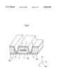
- FIG. 8 is a perspective view illustrating a prior art film carrier signal transmission line.
- reference numeral 1 designates a dielectric film such as polyimide.
- First metal films 3 each comprising a copper thin film or the like and having a predetermined width are disposed on a first or front surface of the dielectric material film 1 as signal lines.
- a second metal film 2 is disposed on a second or rear surface of the dielectric material film 1 as a ground plane.
- This prior art film carrier signal transmission line operates as follows.
- the film carrier signal transmission line as shown in FIG. 8 is used for such as connections between circuits in the same package, in which the copper thin film 2 functions as a ground plane and the copper thin films 3 respectively function as a signal line, and the electro-magnetic wave (hereinafter referred to as RF signal) is transmitted on the transmission line that is constituted by each of the copper thin film signal lines 3 and the copper thin film ground plane 2 of a predetermined line impedance in the Z direction Axes 100 indicate the X, Y, and Z directions.
- RF signal electro-magnetic wave
- the prior art film carrier signal transmission line of the microstrip line structure has the following problems. That is, when the respective signal lines are disposed much closer to each other with increasing integration density, mutual interference, i.e., crosstalk between signal lines, increases and transmission loss increases.
- FIG. 9 illustrates crosstalk between signal lines as shown by arrows 10.
- a film carrier signal transmission line includes a dielectric material having a first or front surface and a second or rear surface opposite the first or front surface, a plurality of signal lines for transmitting a super high frequency signal embedded in the dielectric material film carrier at predetermined intervals, a grounding line or a ground plane disposed on the second or rear surface of the dielectric material film carrier, a separating groove provided at a region of the film carrier between the adjacent signal lines and along the signal lines, and second grounding conductor films disposed on the first surface of the film carrier and in the separating groove, electrically connected with the first grounding conductor film via the separating groove.
- a film carrier signal transmission line includes a dielectric material having a first surface and a second surface opposite the first surface, a plurality of signal lines for transmitting a super high frequency signal embedded in the dielectric material film carrier at predetermined intervals, a grounding line or a ground plane disposed on the second surface of the dielectric material film carrier, a separating groove provided at a region of the film carrier between the adjacent signal lines and along the signal lines, and second grounding conductor films disposed on the first surface of the film carrier and in the separating groove, electrically connected with the first grounding conductor film via the separating groove. Therefore, the film carrier signal transmission line and the circuit can be connected as signal lines of a coplanar type and the impedance mismatching at the connecting part is reduced.
- the signal lines extend out from the film carrier at their ends, and grounding conductor extending portions are provided at both sides of the extending signal lines, the grounding conductor extending portions are connected to the first and second grounding conductor films, end portions of which are connected to each other, and a space between the grounding conductor extending portions is filled with the dielectric material film carrier.
- slits having a predetermined width and depth are provided at the second grounding conductor film above the signal lines. Therefore, the impedance at the end portion of the signal transmission line varies smoothly.
- a film carrier signal transmission line In a film carrier signal transmission line according to a fifth aspect of the present invention, foamed material is employed as the dielectric film material. Therefore, the dielectric constant of the dielectric material constituting the transmission line is reduced.
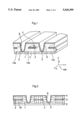
- FIG. 1 is a perspective view illustrating a film carrier signal transmission line in accordance with a first embodiment of the present invention.
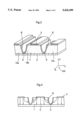
- FIG. 2 is a diagram illustrating the electric field distribution during transmitting signals on the film carrier signal transmission line of the first embodiment.
- FIG. 3 is a perspective view illustrating a film carrier signal transmission line in accordance with a second embodiment of the present invention.
- FIG. 4 is a diagram illustrating the electric field distribution during transmitting signals on the film carrier signal transmission line of the second embodiment.
- FIG. 5 is a perspective view illustrating a film carrier signal transmission line in accordance with a third embodiment of the present invention.
- FIG. 6 is a perspective view illustrating a film carrier signal transmission line in accordance with a fourth embodiment of the present invention.
- FIG. 7 is a perspective view illustrating a film carrier signal transmission line in accordance with a fifth embodiment of the present invention.
- FIG. 8 is a perspective view illustrating a prior art film carrier signal transmission line.
- FIG. 9 is a diagram illustrating the electric field distribution of the signal transmission line of FIG. 8.
- FIG. 1 illustrates a film carrier signal transmission line in accordance with a first embodiment of the present invention.
- reference numeral 1 designates a film carrier comprising polyimide.
- a ground plane 2 comprising a first copper thin film is disposed on the rear surface of the polyimide film 1.
- a second copper thin film 3 as a signal line is provided in the polyimide film at a height h from the ground plane 2 and having a width of w to attain a desired line impedance.
- a third copper thin film 4 is disposed on the surface of the polyimide film laminated on the second layer copper thin film 3 and this copper thin film 4 is connected to the ground plane 2 by the copper thin film 6 produced in the separating groove 5 provided on the polyimide film 1.
- the width of the copper thin film 4 is set so that the copper thin film 6 does not short-circuit with the signal line 3.
- the ground plane 2, and the copper thin films 4 and 6 function as a ground plane or a grounding line for the signal transmission line of copper thin film 3, and the electro-magnetic waves of an electric signal are transmitted in the Z direction on the transmission line of a predetermined line impedance constituted by the copper thin films 2, 3, 4, and 6.
- Axes 100 indicate the X, Y, and Z directions.
- a separating groove 5 is produced between adjacent copper thin films 3 and a copper thin film 6 is disposed in the groove 5, so that the spaces 10a, 10 b, and 10c, as shown in FIG. 1, surrounding each of the adjacent copper thin films 3 are electrically shielded as shown by the electric field lines 10, and generation of crosstalk is prevented, whereby a low loss signal transmission line is realized.
- a polyimide film of a predetermined thickness is produced on the copper thin film 2, copper thin film material to be the signal line is plated on the entire surface thereof, this copper thin film material is processed to a signal line of a predetermined line width by such as photolithography, and further polyimide is deposited thereon, thereby producing a structure with a buried signal line 3 in the polyimide film 1. Then, a copper thin film 4 to be a ground plane is produced on the entire surface of the polyimide film 1. Thereafter, a predetermined portion of the polyimide film 1 is etched employing a solution of ferric chloride. A separating groove 5 which reaches the copper thin film 2 is produced by employing a developer for photolithography and another copper thin film 6 is produced only in the separating groove, thereby producing the structure shown in FIG. 1.
- the copper thin film 3 is surrounded by the grounding conductor, and therefore, crosstalk can be prevented even when adjacent copper thin films 3 are close to each other, and further even when the width of the separating groove 5 is narrowed.
- a signal transmission line advantageous to high density integration is provided.
- FIG. 3 is a diagram showing a film carrier signal transmission line in accordance with a second embodiment of the present invention.
- a micro strip line is constituted by a copper thin film 2 and a signal line 3, and a separating groove 5 reaches the copper thin film 2 on a portion of the polyimide film 1 between the respective signal lines 3, and another copper thin film 6 is disposed in the separating groove 5.
- the ground plane 2 and the copper thin film 6 function as a ground plane or a grounding line
- the copper thin film 3 functions as a signal line
- the electric signal is transmitted on these transmission lines in the Z direction Axes 100 indicate the X, Y, and Z directions.
- the copper thin film 6 connected to the ground plane 2 and having the same grounded voltage is disposed in the separating groove 5 between the adjacent copper thin films 3, the spaces 10a, 10b, and 10c surrounding the respective adjacent copper thin films 3 are electrically shielded from each other by the copper thin film 6 as shown in FIG. 4. Thereby, a low loss signal transmission line is realized.
- the signal line 3 is not buried in the polyimide film 1 and therefore this structure can be easily manufactured relative to the first embodiment.
- FIG. 4 is a diagram illustrating the electric field distribution during the transmission of signals. As illustrated in FIG. 4, a separating groove 5 is produced between adjacent copper thin films 3, and a thin film 6 is disposed in the groove, so that spaces 10a, 10b, and 10c, shown in FIG. 3, adjacent the copper thin films 3 are electrically shielded, as shown by arrows 10 representing electric field lines.
- FIG. 5 illustrates a third embodiment of the present invention.
- the structure of FIG. 1 is modified by using a foamed material 9, for example, low density polyethylene, in place of the polyimide 1, to constitute a carrier signal transmission line.
- a foamed material 9 for example, low density polyethylene
- the ground plane 2 and the copper thin film 4 function as ground planes and the copper thin film 3 functions as a signal line, and the electric signal is transmitted in the Z direction Axis 100 indicate the X, Y, and Z directions.
- FIG. 6 illustrates a fourth embodiment of the present invention.
- the copper thin film 3 in the film carrier signal transmission line of the structure shown in FIG. 1 is taken out at the end of the signal transmission line.
- the copper thin films 7a and 7b connected with the copper thin film 2 and the copper thin film 4, respectively, are provided at the left and right sides of copper thin film 3 and spaces between the copper thin films 7a and 7b are filled with polyimide film 1.
- the top ends of the copper thin films 7a and 7b are both connected to constitute a polyimide tapered copper thin film 7.
- FIG. 7 illustrates a film carrier signal transmission line in accordance with a fifth embodiment of the present invention. As illustrated in FIG. 7, V shaped slits 8 are disposed in the copper thin film 4 located above the copper thin film 3 in the film carrier signal transmission line as shown in FIG. 6.
- the impedance of the signal line 3 at the end part of the signal transmission line gradually varies, and impedance mismatching at the connecting portion of the mounting portion with a semiconductor integrated circuit and connecting portions between a plurality of semiconductor integrated circuits is further reduced.
- foamed material is employed in place of polyimide
- minute hollow spheres (Microballoons from Phyllite, England) can be mixed in the polyimide film with the same effects as described above.
- the shape of the slit is not limited to the V shape and any arbitrary shape which can smoothly vary the impedance at the end of the transmission line can be employed with the same effect as described above.
- the electric signal is transmitted in the Z direction.
- Axes 100 indicate the X, Y, and Z directions.
Abstract
Description
Claims (5)
Applications Claiming Priority (2)
| Application Number | Priority Date | Filing Date | Title |
|---|---|---|---|
| JP5-017186 | 1993-02-04 | ||
| JP01718693A JP3241139B2 (en) | 1993-02-04 | 1993-02-04 | Film carrier signal transmission line |
Publications (1)
| Publication Number | Publication Date |
|---|---|
| US5426399A true US5426399A (en) | 1995-06-20 |
Family
ID=11936919
Family Applications (1)
| Application Number | Title | Priority Date | Filing Date |
|---|---|---|---|
| US08/165,343 Expired - Lifetime US5426399A (en) | 1993-02-04 | 1993-12-13 | Film carrier signal transmission line having separating grooves |
Country Status (4)
| Country | Link |
|---|---|
| US (1) | US5426399A (en) |
| JP (1) | JP3241139B2 (en) |
| DE (1) | DE4402082A1 (en) |
| GB (1) | GB2274946B (en) |
Cited By (74)
| Publication number | Priority date | Publication date | Assignee | Title |
|---|---|---|---|---|
| WO1996026555A1 (en) * | 1995-02-23 | 1996-08-29 | Superconductor Technologies, Inc. | Method and apparatus for increasing power handling capabilities of high temperature superconducting devices |
| US5631446A (en) * | 1995-06-07 | 1997-05-20 | Hughes Electronics | Microstrip flexible printed wiring board interconnect line |
| US5652557A (en) * | 1994-10-19 | 1997-07-29 | Mitsubishi Denki Kabushiki Kaisha | Transmission lines and fabricating method thereof |
| US5741144A (en) * | 1995-06-12 | 1998-04-21 | Berg Technology, Inc. | Low cross and impedance controlled electric connector |
| US5764119A (en) * | 1995-10-16 | 1998-06-09 | Kabushiki Kaisha Toshiba | Wiring board for high-frequency signals and semiconductor module for high-frequency signals using the wiring board |
| US5777526A (en) * | 1994-09-01 | 1998-07-07 | Hitachi, Ltd. | Method of manufacturing a microstrip transmission device |
| US5817973A (en) * | 1995-06-12 | 1998-10-06 | Berg Technology, Inc. | Low cross talk and impedance controlled electrical cable assembly |
| US5922650A (en) * | 1995-05-01 | 1999-07-13 | Com Dev Ltd. | Method and structure for high power HTS transmission lines using strips separated by a gap |
| WO2000038271A1 (en) * | 1998-12-22 | 2000-06-29 | Lk A/S | An electrical cable |
| WO2000047026A1 (en) * | 1999-02-02 | 2000-08-10 | Telefonaktiebolaget Lm Ericsson (Publ) | An arrangement relating to conductor carriers and methods for the manufacture of such carriers |
| US6131269A (en) * | 1998-05-18 | 2000-10-17 | Trw Inc. | Circuit isolation technique for RF and millimeter-wave modules |
| DE19920593A1 (en) * | 1999-05-05 | 2000-11-23 | David Finn | Chip carrier for a chip module and method for producing the chip module |
| US6162993A (en) * | 1997-01-17 | 2000-12-19 | Stemmann-Technik Gmbh | Signal conductor |
| US6210182B1 (en) | 1995-06-12 | 2001-04-03 | Berg Technology, Inc. | Low cross talk and impedance controlled electrical connector |
| US6281780B1 (en) * | 1999-04-28 | 2001-08-28 | Texas Instruments Incorporated | Electrical apparatus having improved electrical contact and electrical contact used therewith |
| EP1127387A1 (en) * | 1998-09-10 | 2001-08-29 | Viasystems Group, Inc. | Non-circular micro-via |
| US6313718B1 (en) | 1998-11-19 | 2001-11-06 | U.S. Philips Corporation | High frequency dielectric device |
| US6433408B1 (en) * | 1999-01-08 | 2002-08-13 | Nec Corporation | Highly integrated circuit including transmission lines which have excellent characteristics |
| US6486394B1 (en) * | 1996-07-31 | 2002-11-26 | Dyconex Patente Ag | Process for producing connecting conductors |
| US20020192901A1 (en) * | 1995-11-20 | 2002-12-19 | Shinichiro Kimura | Semiconductor memory device and manufacturing method thereof |
| US6512423B2 (en) * | 2000-09-28 | 2003-01-28 | Kabushiki Kaisha Toshiba | Printed board, method for producing the same, and electronic device having the same |
| US6535089B1 (en) * | 1999-06-03 | 2003-03-18 | Murata Manufacturing Co. Ltd. | High-frequency circuit device and communication apparatus using the same |
| WO2003067943A2 (en) * | 2002-02-04 | 2003-08-14 | Intel Corporation | Power-ground plane partitioning and via connection to utilize channel/trenches for power delivery |
| US6653915B1 (en) | 1998-04-16 | 2003-11-25 | Motorola, Inc. | Coaxial transmission lines having grounding troughs on a printed circuit board |
| US20030222738A1 (en) * | 2001-12-03 | 2003-12-04 | Memgen Corporation | Miniature RF and microwave components and methods for fabricating such components |
| US20040112617A1 (en) * | 1998-09-10 | 2004-06-17 | Cotton Martin A. | Non-circular micro-via |
| US6756673B2 (en) * | 2001-04-17 | 2004-06-29 | Micron Technology, Inc. | Low-loss coplanar waveguides and method of fabrication |
| US20040124955A1 (en) * | 2002-12-31 | 2004-07-01 | Sung-Mao Wu | High frequency substrate |
| US20040140862A1 (en) * | 2001-12-03 | 2004-07-22 | Memgen Corporation | Miniature RF and microwave components and methods for fabricating such components |
| US20040174223A1 (en) * | 2003-03-05 | 2004-09-09 | Dutta Achyut | High speed electronics interconnect and method of manufacture |
| US20040211585A1 (en) * | 2003-03-07 | 2004-10-28 | Nicholas Jordan | Flat flexible cable |
| US20040251042A1 (en) * | 2003-04-02 | 2004-12-16 | Biophan Technologies, Inc. | Device and method for preventing magnetic-resonance imaging induced damage |
| US20040258841A1 (en) * | 2003-06-19 | 2004-12-23 | Casey John F. | Methods for depositing a thickfilm dielectric on a substrate |
| US20040256350A1 (en) * | 2003-06-19 | 2004-12-23 | Casey John F. | Methods for forming a conductor on a dielectric |
| US20050082087A1 (en) * | 2003-10-21 | 2005-04-21 | International Business Machines Corporation | Dielectric structure for printed circuit board traces |
| US20050151604A1 (en) * | 2003-12-24 | 2005-07-14 | Brunker David L. | Triangular conforming transmission structure |
| US20050156692A1 (en) * | 2004-01-20 | 2005-07-21 | Dove Lewis R. | Double density quasi-coax transmission lines |
| US20050156693A1 (en) * | 2004-01-20 | 2005-07-21 | Dove Lewis R. | Quasi-coax transmission lines |
| US20050191412A1 (en) * | 2003-06-19 | 2005-09-01 | Casey John F. | Methods for making microwave circuits |
| US6939173B1 (en) | 1995-06-12 | 2005-09-06 | Fci Americas Technology, Inc. | Low cross talk and impedance controlled electrical connector with solder masses |
| US20050195052A1 (en) * | 2004-03-03 | 2005-09-08 | Dove Lewis R. | Methods and apparatus for printing conductive thickfilms over thickfilm dielectrics |
| US20060001154A1 (en) * | 2004-06-30 | 2006-01-05 | Stoneham Edward B | Chip-to-chip trench circuit structure |
| US20060001129A1 (en) * | 2004-06-30 | 2006-01-05 | Stoneham Edward B | Component interconnect with substrate shielding |
| US20060011384A1 (en) * | 2004-07-13 | 2006-01-19 | Herman Kwong | Reducing or eliminating cross-talk at device-substrate interface |
| US20060077021A1 (en) * | 2004-01-14 | 2006-04-13 | Peterson Kent E | Slow-wave structure for ridge waveguide |
| US20060139117A1 (en) * | 2004-12-23 | 2006-06-29 | Brunker David L | Multi-channel waveguide structure |
| US20060289979A1 (en) * | 2003-08-26 | 2006-12-28 | God Ralf | Bridge modules for smart labels |
| US20070145595A1 (en) * | 2005-12-27 | 2007-06-28 | Hall Stephen H | High speed interconnect |
| US20070183131A1 (en) * | 2006-01-25 | 2007-08-09 | Industrial Technology Research Institute | Mirror image shielding structure |
| US20080048796A1 (en) * | 2006-08-22 | 2008-02-28 | Yigal Shaul | High speed signal transmission |
| US20080197945A1 (en) * | 2007-02-15 | 2008-08-21 | Motorola, Inc. | High frequency coplanar strip transmission line on a lossy substrate |
| US20080309349A1 (en) * | 2007-06-15 | 2008-12-18 | Computer Access Technology Corporation | Flexible interposer system |
| US20100046079A1 (en) * | 2004-02-12 | 2010-02-25 | Jun-Bo Yoon | Polymer pattern and metal film pattern, metal pattern, plastic mold using thereof, and method of the forming the same |
| US20100194500A1 (en) * | 2009-02-05 | 2010-08-05 | Fujikura Ltd. | Leaky cable |
| US20100206617A1 (en) * | 2009-02-17 | 2010-08-19 | Lockheed Martin Corporation | Electrical isolating structure for conductors in a substrate |
| US20100237967A1 (en) * | 2007-10-09 | 2010-09-23 | Hiroaki Ueno | Circuit device |
| US7804029B1 (en) * | 2008-12-05 | 2010-09-28 | The United States Of America As Represented By The United States Department Of Energy | Electromagnetic wrap |
| US20100259337A1 (en) * | 2009-04-10 | 2010-10-14 | Broadcom Corporation | High speed transmission lines with enhanced coupling |
| CN106332435A (en) * | 2015-06-24 | 2017-01-11 | 宏启胜精密电子(秦皇岛)有限公司 | Flexible printed circuit board and manufacturing method therefor |
| US20170086288A1 (en) * | 2015-09-23 | 2017-03-23 | Intel Corporation | Interconnects with trenches |
| WO2017053205A1 (en) * | 2015-09-24 | 2017-03-30 | Qualcomm Incorporated | High-density stacked grounded coplanar waveguides |
| US9614266B2 (en) | 2001-12-03 | 2017-04-04 | Microfabrica Inc. | Miniature RF and microwave components and methods for fabricating such components |
| CN108878020A (en) * | 2018-05-31 | 2018-11-23 | 维沃移动通信有限公司 | A kind of signal transmssion line and terminal device |
| US10297421B1 (en) | 2003-05-07 | 2019-05-21 | Microfabrica Inc. | Plasma etching of dielectric sacrificial material from reentrant multi-layer metal structures |
| EP3531449A4 (en) * | 2016-10-21 | 2020-04-08 | Kyocera Corporation | High frequency base body, high frequency package, and high frequency module |
| CN111567148A (en) * | 2017-11-10 | 2020-08-21 | 雷神公司 | Additive Manufacturing Technology (AMT) Faraday boundaries in radio frequency circuits |
| US10826147B2 (en) | 2017-11-10 | 2020-11-03 | Raytheon Company | Radio frequency circuit with a multi-layer transmission line assembly having a conductively filled trench surrounding the transmission line |
| US10849219B2 (en) | 2018-02-28 | 2020-11-24 | Raytheon Company | SNAP-RF interconnections |
| US11089687B2 (en) | 2018-02-28 | 2021-08-10 | Raytheon Company | Additive manufacturing technology (AMT) low profile signal divider |
| US11121474B2 (en) | 2017-11-10 | 2021-09-14 | Raytheon Company | Additive manufacturing technology (AMT) low profile radiator |
| TWI748191B (en) * | 2018-07-06 | 2021-12-01 | 日商天龍精機股份有限公司 | Transmission line, transmission line manufacturing method, and transmission line manufacturing device |
| US11289814B2 (en) | 2017-11-10 | 2022-03-29 | Raytheon Company | Spiral antenna and related fabrication techniques |
| US11343912B2 (en) * | 2019-11-26 | 2022-05-24 | Nec Corporation | Electronic circuit apparatus |
| CN114631226A (en) * | 2019-10-29 | 2022-06-14 | 日本电信电话株式会社 | High-frequency line connection structure |
Families Citing this family (12)
| Publication number | Priority date | Publication date | Assignee | Title |
|---|---|---|---|---|
| DE4446509A1 (en) * | 1994-12-24 | 1996-06-27 | Sel Alcatel Ag | Method for producing conductor tracks on a substrate having depressions |
| GB9621353D0 (en) | 1996-10-11 | 1996-12-04 | Tunewell Technology Ltd | Improvements in or relating to a power distribution system |
| KR100308871B1 (en) * | 1998-12-28 | 2001-11-03 | 윤덕용 | coaxial type signal line and fabricating method thereof |
| JP3615126B2 (en) | 2000-07-11 | 2005-01-26 | 寛治 大塚 | Semiconductor circuit device |
| JP3741603B2 (en) * | 2000-11-17 | 2006-02-01 | 寛治 大塚 | Wiring board |
| JP4919755B2 (en) * | 2006-10-02 | 2012-04-18 | 日東電工株式会社 | Wiring circuit board and electronic equipment |
| JP2008311682A (en) * | 2008-09-16 | 2008-12-25 | Kyocera Corp | Wiring board |
| US8279611B2 (en) | 2009-12-09 | 2012-10-02 | Research In Motion Limited | Flexible cable having rectangular waveguide formed therein and methods of manufacturing same |
| EP2334156A1 (en) * | 2009-12-09 | 2011-06-15 | Research In Motion Limited | Flexible cable and methods of manufacturing same |
| KR101527379B1 (en) * | 2014-07-14 | 2015-06-09 | 와이엠티 주식회사 | Semiconductor package and manufacturing methode of the same |
| WO2018020919A1 (en) * | 2016-07-29 | 2018-02-01 | 株式会社村田製作所 | Transmission line and electronic device |
| JP6655577B2 (en) * | 2017-04-03 | 2020-02-26 | 矢崎総業株式会社 | Transmission line and manufacturing method thereof |
Citations (10)
| Publication number | Priority date | Publication date | Assignee | Title |
|---|---|---|---|---|
| US3370256A (en) * | 1964-09-14 | 1968-02-20 | Gen Electric | Variable delay line |
| GB1243764A (en) * | 1969-04-29 | 1971-08-25 | Bunker Ramo | Method of fabricating coaxial circuitry |
| DD155025A1 (en) * | 1980-10-22 | 1982-05-05 | Canzler Fritz Eberhard | SHIELDED FLATBAND CABLE |
| JPS61277111A (en) * | 1985-05-31 | 1986-12-08 | 株式会社 潤工社 | Balance transmission line |
| JPH01146426A (en) * | 1987-12-02 | 1989-06-08 | Mitsubishi Electric Corp | Pll circuit |
| US4845311A (en) * | 1988-07-21 | 1989-07-04 | Hughes Aircraft Company | Flexible coaxial cable apparatus and method |
| JPH0341803A (en) * | 1989-07-07 | 1991-02-22 | Hitachi Chem Co Ltd | Wiring board with reduced crosstalk noise between signal lines and its manufacture |
| JPH03211870A (en) * | 1990-01-17 | 1991-09-17 | Toshiba Corp | Monolithic microwave integrated circuit |
| JPH04294602A (en) * | 1991-03-23 | 1992-10-19 | Nec Corp | Microwave circuit board |
| WO1992022939A1 (en) * | 1991-06-14 | 1992-12-23 | Telefonaktiebolaget Lm Ericsson | A device with flexible, stripline conductors and a method of manufacturing such a device |
Family Cites Families (3)
| Publication number | Priority date | Publication date | Assignee | Title |
|---|---|---|---|---|
| JP2541268B2 (en) * | 1988-02-16 | 1996-10-09 | 富士通株式会社 | Lead structure of semiconductor device |
| DE3812414A1 (en) * | 1988-04-14 | 1989-10-26 | Standard Elektrik Lorenz Ag | METHOD FOR PRODUCING AN ALL-SIDED SHIELDED SIGNAL LINE |
| JP2754401B2 (en) * | 1989-06-01 | 1998-05-20 | 新光電気工業株式会社 | Package for electronic components |
-
1993
- 1993-02-04 JP JP01718693A patent/JP3241139B2/en not_active Expired - Fee Related
- 1993-12-08 GB GB9325152A patent/GB2274946B/en not_active Expired - Fee Related
- 1993-12-13 US US08/165,343 patent/US5426399A/en not_active Expired - Lifetime
-
1994
- 1994-01-25 DE DE4402082A patent/DE4402082A1/en not_active Ceased
Patent Citations (10)
| Publication number | Priority date | Publication date | Assignee | Title |
|---|---|---|---|---|
| US3370256A (en) * | 1964-09-14 | 1968-02-20 | Gen Electric | Variable delay line |
| GB1243764A (en) * | 1969-04-29 | 1971-08-25 | Bunker Ramo | Method of fabricating coaxial circuitry |
| DD155025A1 (en) * | 1980-10-22 | 1982-05-05 | Canzler Fritz Eberhard | SHIELDED FLATBAND CABLE |
| JPS61277111A (en) * | 1985-05-31 | 1986-12-08 | 株式会社 潤工社 | Balance transmission line |
| JPH01146426A (en) * | 1987-12-02 | 1989-06-08 | Mitsubishi Electric Corp | Pll circuit |
| US4845311A (en) * | 1988-07-21 | 1989-07-04 | Hughes Aircraft Company | Flexible coaxial cable apparatus and method |
| JPH0341803A (en) * | 1989-07-07 | 1991-02-22 | Hitachi Chem Co Ltd | Wiring board with reduced crosstalk noise between signal lines and its manufacture |
| JPH03211870A (en) * | 1990-01-17 | 1991-09-17 | Toshiba Corp | Monolithic microwave integrated circuit |
| JPH04294602A (en) * | 1991-03-23 | 1992-10-19 | Nec Corp | Microwave circuit board |
| WO1992022939A1 (en) * | 1991-06-14 | 1992-12-23 | Telefonaktiebolaget Lm Ericsson | A device with flexible, stripline conductors and a method of manufacturing such a device |
Cited By (149)
| Publication number | Priority date | Publication date | Assignee | Title |
|---|---|---|---|---|
| US5777526A (en) * | 1994-09-01 | 1998-07-07 | Hitachi, Ltd. | Method of manufacturing a microstrip transmission device |
| US5652557A (en) * | 1994-10-19 | 1997-07-29 | Mitsubishi Denki Kabushiki Kaisha | Transmission lines and fabricating method thereof |
| WO1996026555A1 (en) * | 1995-02-23 | 1996-08-29 | Superconductor Technologies, Inc. | Method and apparatus for increasing power handling capabilities of high temperature superconducting devices |
| US5922650A (en) * | 1995-05-01 | 1999-07-13 | Com Dev Ltd. | Method and structure for high power HTS transmission lines using strips separated by a gap |
| US5631446A (en) * | 1995-06-07 | 1997-05-20 | Hughes Electronics | Microstrip flexible printed wiring board interconnect line |
| US6146203A (en) * | 1995-06-12 | 2000-11-14 | Berg Technology, Inc. | Low cross talk and impedance controlled electrical connector |
| US5817973A (en) * | 1995-06-12 | 1998-10-06 | Berg Technology, Inc. | Low cross talk and impedance controlled electrical cable assembly |
| US6939173B1 (en) | 1995-06-12 | 2005-09-06 | Fci Americas Technology, Inc. | Low cross talk and impedance controlled electrical connector with solder masses |
| US6133523A (en) * | 1995-06-12 | 2000-10-17 | Berg Technology, Inc. | Low cross talk and impedance controlled electrical cable assembly |
| US5741144A (en) * | 1995-06-12 | 1998-04-21 | Berg Technology, Inc. | Low cross and impedance controlled electric connector |
| US6476316B1 (en) | 1995-06-12 | 2002-11-05 | Fci Americas Technology, Inc. | Low cross talk and impedance controlled electrical cable assembly |
| US6210182B1 (en) | 1995-06-12 | 2001-04-03 | Berg Technology, Inc. | Low cross talk and impedance controlled electrical connector |
| US5764119A (en) * | 1995-10-16 | 1998-06-09 | Kabushiki Kaisha Toshiba | Wiring board for high-frequency signals and semiconductor module for high-frequency signals using the wiring board |
| US20050045933A1 (en) * | 1995-11-20 | 2005-03-03 | Shinichiro Kimura | Semiconductor memory device and manufacturing method thereof |
| US7196368B2 (en) | 1995-11-20 | 2007-03-27 | Renesas Technology Corp. | Semiconductor memory arrangements with crown shaped capacitor arrangements trenched in interlayer dielectric film |
| US20020192901A1 (en) * | 1995-11-20 | 2002-12-19 | Shinichiro Kimura | Semiconductor memory device and manufacturing method thereof |
| US6791134B2 (en) * | 1995-11-20 | 2004-09-14 | Hitachi, Ltd. | Semiconductor memory device and manufacturing method thereof |
| US6486394B1 (en) * | 1996-07-31 | 2002-11-26 | Dyconex Patente Ag | Process for producing connecting conductors |
| US6162993A (en) * | 1997-01-17 | 2000-12-19 | Stemmann-Technik Gmbh | Signal conductor |
| US6653915B1 (en) | 1998-04-16 | 2003-11-25 | Motorola, Inc. | Coaxial transmission lines having grounding troughs on a printed circuit board |
| US6131269A (en) * | 1998-05-18 | 2000-10-17 | Trw Inc. | Circuit isolation technique for RF and millimeter-wave modules |
| EP1127387A1 (en) * | 1998-09-10 | 2001-08-29 | Viasystems Group, Inc. | Non-circular micro-via |
| US20040112617A1 (en) * | 1998-09-10 | 2004-06-17 | Cotton Martin A. | Non-circular micro-via |
| EP1127387A4 (en) * | 1998-09-10 | 2004-05-26 | Viasystems Group Inc | Non-circular micro-via |
| US6313718B1 (en) | 1998-11-19 | 2001-11-06 | U.S. Philips Corporation | High frequency dielectric device |
| US6590161B1 (en) | 1998-12-22 | 2003-07-08 | Lk A/S | Electrical cable |
| WO2000038271A1 (en) * | 1998-12-22 | 2000-06-29 | Lk A/S | An electrical cable |
| US6433408B1 (en) * | 1999-01-08 | 2002-08-13 | Nec Corporation | Highly integrated circuit including transmission lines which have excellent characteristics |
| US6617509B1 (en) | 1999-02-02 | 2003-09-09 | Telefonaktiebolaget Lm Ericsson (Publ) | Arrangement relating to conductor carriers and methods for the manufacture of such carriers |
| WO2000047026A1 (en) * | 1999-02-02 | 2000-08-10 | Telefonaktiebolaget Lm Ericsson (Publ) | An arrangement relating to conductor carriers and methods for the manufacture of such carriers |
| US6281780B1 (en) * | 1999-04-28 | 2001-08-28 | Texas Instruments Incorporated | Electrical apparatus having improved electrical contact and electrical contact used therewith |
| DE19920593B4 (en) * | 1999-05-05 | 2006-07-13 | Assa Abloy Identification Technology Group Ab | Chip carrier for a chip module and method for producing the chip module |
| US7105915B1 (en) | 1999-05-05 | 2006-09-12 | David Finn | Chip carrier a chip module and method of manufacturing the chip module |
| DE19920593A1 (en) * | 1999-05-05 | 2000-11-23 | David Finn | Chip carrier for a chip module and method for producing the chip module |
| US6535089B1 (en) * | 1999-06-03 | 2003-03-18 | Murata Manufacturing Co. Ltd. | High-frequency circuit device and communication apparatus using the same |
| US6512423B2 (en) * | 2000-09-28 | 2003-01-28 | Kabushiki Kaisha Toshiba | Printed board, method for producing the same, and electronic device having the same |
| US20040171249A1 (en) * | 2001-04-17 | 2004-09-02 | Ahn Kie Y. | Low-loss coplanar waveguides and method of fabrication |
| US20040124956A1 (en) * | 2001-04-17 | 2004-07-01 | Ahn Kie Y. | Low-loss coplanar waveguides |
| US6953996B2 (en) * | 2001-04-17 | 2005-10-11 | Micron Technology, Inc. | Low-loss coplanar waveguides and method of fabrication |
| US7064438B2 (en) | 2001-04-17 | 2006-06-20 | Micron Technology, Inc. | Low-loss coplanar waveguides |
| US7084058B2 (en) | 2001-04-17 | 2006-08-01 | Micron Technology Inc. | Method of forming low-loss coplanar waveguides |
| US6756673B2 (en) * | 2001-04-17 | 2004-06-29 | Micron Technology, Inc. | Low-loss coplanar waveguides and method of fabrication |
| US7259640B2 (en) | 2001-12-03 | 2007-08-21 | Microfabrica | Miniature RF and microwave components and methods for fabricating such components |
| US20080246558A1 (en) * | 2001-12-03 | 2008-10-09 | Microfabrica Inc. | Miniature RF and Microwave Components and Methods for Fabricating Such Components |
| US7239219B2 (en) | 2001-12-03 | 2007-07-03 | Microfabrica Inc. | Miniature RF and microwave components and methods for fabricating such components |
| US8713788B2 (en) | 2001-12-03 | 2014-05-06 | Microfabrica Inc. | Method for fabricating miniature structures or devices such as RF and microwave components |
| US11145947B2 (en) | 2001-12-03 | 2021-10-12 | Microfabrica Inc. | Miniature RF and microwave components and methods for fabricating such components |
| US20030222738A1 (en) * | 2001-12-03 | 2003-12-04 | Memgen Corporation | Miniature RF and microwave components and methods for fabricating such components |
| US7830228B2 (en) | 2001-12-03 | 2010-11-09 | Microfabrica Inc. | Miniature RF and microwave components and methods for fabricating such components |
| US9620834B2 (en) | 2001-12-03 | 2017-04-11 | Microfabrica Inc. | Method for fabricating miniature structures or devices such as RF and microwave components |
| US9614266B2 (en) | 2001-12-03 | 2017-04-04 | Microfabrica Inc. | Miniature RF and microwave components and methods for fabricating such components |
| US20040140862A1 (en) * | 2001-12-03 | 2004-07-22 | Memgen Corporation | Miniature RF and microwave components and methods for fabricating such components |
| US8056221B2 (en) | 2002-02-04 | 2011-11-15 | Intel Corporation | Power-ground plane partitioning and via connection to utilize channel/trenches for power delivery |
| CN1625925B (en) * | 2002-02-04 | 2010-05-26 | 英特尔公司 | Power-ground plane partitioning and via connection to utilize channel/trenches for power delivery |
| WO2003067943A2 (en) * | 2002-02-04 | 2003-08-14 | Intel Corporation | Power-ground plane partitioning and via connection to utilize channel/trenches for power delivery |
| US20030205407A1 (en) * | 2002-02-04 | 2003-11-06 | Brist Gary A. | Power-ground plane partitioning and via connection to utilize channel/trenches for power delivery |
| WO2003067943A3 (en) * | 2002-02-04 | 2003-11-06 | Intel Corp | Power-ground plane partitioning and via connection to utilize channel/trenches for power delivery |
| US6747216B2 (en) | 2002-02-04 | 2004-06-08 | Intel Corporation | Power-ground plane partitioning and via connection to utilize channel/trenches for power delivery |
| US8299369B2 (en) * | 2002-02-04 | 2012-10-30 | Intel Corporation | Power-ground plane partitioning and via connection to utilize channel/trenches for power delivery |
| US20080029295A1 (en) * | 2002-02-04 | 2008-02-07 | Brist Gary A | Power-ground plane partitioning and via connection to utilize channel/trenches for power delivery |
| US20080029296A1 (en) * | 2002-02-04 | 2008-02-07 | Brist Gary A | Power-ground plane partitioning and via connection to utilize channel/trenches for power delivery |
| US7797826B2 (en) | 2002-02-04 | 2010-09-21 | Intel Corporation | Method of power-ground plane partitioning to utilize channel/trenches |
| US7269899B2 (en) | 2002-02-04 | 2007-09-18 | Intel Corporation | Method for creating power-ground plane partitioning and via connection to utilize channel/trenches for power delivery |
| US20100038127A1 (en) * | 2002-02-04 | 2010-02-18 | Brist Gary A | Power-Ground Plane Partitioning and Via Connection to Utilize Channel/Trenches for Power Delivery |
| US20040124955A1 (en) * | 2002-12-31 | 2004-07-01 | Sung-Mao Wu | High frequency substrate |
| US7432775B2 (en) * | 2003-03-05 | 2008-10-07 | Banpil Photonics, Inc. | High speed electronics interconnect having a dielectric system with cylindrical holes therein |
| US20040174223A1 (en) * | 2003-03-05 | 2004-09-09 | Dutta Achyut | High speed electronics interconnect and method of manufacture |
| US20040211585A1 (en) * | 2003-03-07 | 2004-10-28 | Nicholas Jordan | Flat flexible cable |
| US7738942B2 (en) | 2003-04-02 | 2010-06-15 | Medtronic, Inc. | Device and method for preventing magnetic-resonance imaging induced damage |
| US20040251042A1 (en) * | 2003-04-02 | 2004-12-16 | Biophan Technologies, Inc. | Device and method for preventing magnetic-resonance imaging induced damage |
| US20050113876A1 (en) * | 2003-04-02 | 2005-05-26 | Biophan Technologies, Inc. | Device and method for preventing magnetic-resonance imaging induced damage |
| US20050113874A1 (en) * | 2003-04-02 | 2005-05-26 | Biophan Technologies, Inc. | Device and method for preventing magnetic-resonance imaging induced damage |
| US20050113669A1 (en) * | 2003-04-02 | 2005-05-26 | Biophan Technologies, Inc. | Device and method for preventing magnetic-resonance imaging induced damage |
| US8323768B2 (en) | 2003-04-02 | 2012-12-04 | Medtronic, Inc. | Device and method for preventing magnetic-resonance imaging induced damage |
| US7015393B2 (en) * | 2003-04-02 | 2006-03-21 | Biophan Technologies, Inc. | Device and method for preventing magnetic-resonance imaging induced damage |
| US20050113873A1 (en) * | 2003-04-02 | 2005-05-26 | Biophan Technologies, Inc. | Device and method for preventing magnetic-resonance imaging induced damage |
| US20050113676A1 (en) * | 2003-04-02 | 2005-05-26 | Biophan Technologies, Inc. | Device and method for preventing magnetic-resonance imaging induced damage |
| US10297421B1 (en) | 2003-05-07 | 2019-05-21 | Microfabrica Inc. | Plasma etching of dielectric sacrificial material from reentrant multi-layer metal structures |
| US11211228B1 (en) | 2003-05-07 | 2021-12-28 | Microfabrica Inc. | Neutral radical etching of dielectric sacrificial material from reentrant multi-layer metal structures |
| US7265043B2 (en) | 2003-06-19 | 2007-09-04 | Agilent Technologies, Inc. | Methods for making microwave circuits |
| US7125752B2 (en) | 2003-06-19 | 2006-10-24 | Agilent Technologies, Inc. | Methods for making microwave circuits including a ground plane |
| US20040256350A1 (en) * | 2003-06-19 | 2004-12-23 | Casey John F. | Methods for forming a conductor on a dielectric |
| US20050191412A1 (en) * | 2003-06-19 | 2005-09-01 | Casey John F. | Methods for making microwave circuits |
| US20060286722A1 (en) * | 2003-06-19 | 2006-12-21 | Casey John F | Methods for making microwave circuits |
| US7022251B2 (en) | 2003-06-19 | 2006-04-04 | Agilent Technologies, Inc. | Methods for forming a conductor on a dielectric |
| US20040258841A1 (en) * | 2003-06-19 | 2004-12-23 | Casey John F. | Methods for depositing a thickfilm dielectric on a substrate |
| US20060289979A1 (en) * | 2003-08-26 | 2006-12-28 | God Ralf | Bridge modules for smart labels |
| US7186924B2 (en) * | 2003-10-21 | 2007-03-06 | International Business Machines Corporation | Dielectric structure for printed circuit board traces |
| US20050082087A1 (en) * | 2003-10-21 | 2005-04-21 | International Business Machines Corporation | Dielectric structure for printed circuit board traces |
| US20050151604A1 (en) * | 2003-12-24 | 2005-07-14 | Brunker David L. | Triangular conforming transmission structure |
| US7263760B2 (en) * | 2004-01-14 | 2007-09-04 | Peterson Kent E | Method for making a slow-wave ridge waveguide structure |
| US20060077021A1 (en) * | 2004-01-14 | 2006-04-13 | Peterson Kent E | Slow-wave structure for ridge waveguide |
| US20050156692A1 (en) * | 2004-01-20 | 2005-07-21 | Dove Lewis R. | Double density quasi-coax transmission lines |
| US20050156693A1 (en) * | 2004-01-20 | 2005-07-21 | Dove Lewis R. | Quasi-coax transmission lines |
| US20100046079A1 (en) * | 2004-02-12 | 2010-02-25 | Jun-Bo Yoon | Polymer pattern and metal film pattern, metal pattern, plastic mold using thereof, and method of the forming the same |
| US7014784B2 (en) | 2004-03-03 | 2006-03-21 | Agilent Technologies, Inc. | Methods and apparatus for printing conductive thickfilms over thickfilm dielectrics |
| US20050195052A1 (en) * | 2004-03-03 | 2005-09-08 | Dove Lewis R. | Methods and apparatus for printing conductive thickfilms over thickfilm dielectrics |
| US7588966B2 (en) | 2004-06-30 | 2009-09-15 | Endwave Corporation | Chip mounting with flowable layer |
| US7411279B2 (en) | 2004-06-30 | 2008-08-12 | Endwave Corporation | Component interconnect with substrate shielding |
| US7348666B2 (en) | 2004-06-30 | 2008-03-25 | Endwave Corporation | Chip-to-chip trench circuit structure |
| US20080153206A1 (en) * | 2004-06-30 | 2008-06-26 | Endwave Corporation | Chip mounting with flowable layer |
| US20060001129A1 (en) * | 2004-06-30 | 2006-01-05 | Stoneham Edward B | Component interconnect with substrate shielding |
| US20060001154A1 (en) * | 2004-06-30 | 2006-01-05 | Stoneham Edward B | Chip-to-chip trench circuit structure |
| US7145083B2 (en) * | 2004-07-13 | 2006-12-05 | Nortel Networks Limited | Reducing or eliminating cross-talk at device-substrate interface |
| US20060011384A1 (en) * | 2004-07-13 | 2006-01-19 | Herman Kwong | Reducing or eliminating cross-talk at device-substrate interface |
| US20060139117A1 (en) * | 2004-12-23 | 2006-06-29 | Brunker David L | Multi-channel waveguide structure |
| US8732942B2 (en) | 2005-12-27 | 2014-05-27 | Intel Corporation | Method of forming a high speed interconnect |
| US20080172872A1 (en) * | 2005-12-27 | 2008-07-24 | Intel Corporation | High speed interconnect |
| US20070145595A1 (en) * | 2005-12-27 | 2007-06-28 | Hall Stephen H | High speed interconnect |
| US7764512B2 (en) * | 2006-01-25 | 2010-07-27 | Industrial Technology Research Institute | Mirror image shielding structure |
| US20100226112A1 (en) * | 2006-01-25 | 2010-09-09 | Industrial Technology Research Institute | Mirror image shielding structure |
| US20070183131A1 (en) * | 2006-01-25 | 2007-08-09 | Industrial Technology Research Institute | Mirror image shielding structure |
| US8179695B2 (en) | 2006-01-25 | 2012-05-15 | Industrial Technology Research Institute | Mirror image shielding structure |
| US20080048796A1 (en) * | 2006-08-22 | 2008-02-28 | Yigal Shaul | High speed signal transmission |
| US7659790B2 (en) * | 2006-08-22 | 2010-02-09 | Lecroy Corporation | High speed signal transmission line having reduced thickness regions |
| US7791437B2 (en) * | 2007-02-15 | 2010-09-07 | Motorola, Inc. | High frequency coplanar strip transmission line on a lossy substrate |
| US20080197945A1 (en) * | 2007-02-15 | 2008-08-21 | Motorola, Inc. | High frequency coplanar strip transmission line on a lossy substrate |
| US20080309349A1 (en) * | 2007-06-15 | 2008-12-18 | Computer Access Technology Corporation | Flexible interposer system |
| US20100237967A1 (en) * | 2007-10-09 | 2010-09-23 | Hiroaki Ueno | Circuit device |
| US8400237B2 (en) * | 2007-10-09 | 2013-03-19 | Panasonic Corporation | Circuit device including a nano-composite dielectric film |
| US7804029B1 (en) * | 2008-12-05 | 2010-09-28 | The United States Of America As Represented By The United States Department Of Energy | Electromagnetic wrap |
| US8384499B2 (en) * | 2009-02-05 | 2013-02-26 | Fujikura Ltd. | Leaky cable having at least one slot row for propagating electromagnetic waves that have been diffracted backwards |
| US20100194500A1 (en) * | 2009-02-05 | 2010-08-05 | Fujikura Ltd. | Leaky cable |
| US8134086B2 (en) * | 2009-02-17 | 2012-03-13 | Lockheed Martin Corporation | Electrical isolating structure for conductors in a substrate |
| US20100206617A1 (en) * | 2009-02-17 | 2010-08-19 | Lockheed Martin Corporation | Electrical isolating structure for conductors in a substrate |
| US8125289B2 (en) * | 2009-04-10 | 2012-02-28 | Broadcom Corporation | Transmission line pairs with enhanced coupling therebetween and negligible coupling to ground |
| US20100259337A1 (en) * | 2009-04-10 | 2010-10-14 | Broadcom Corporation | High speed transmission lines with enhanced coupling |
| CN106332435A (en) * | 2015-06-24 | 2017-01-11 | 宏启胜精密电子(秦皇岛)有限公司 | Flexible printed circuit board and manufacturing method therefor |
| CN106332435B (en) * | 2015-06-24 | 2019-01-25 | 鹏鼎控股(深圳)股份有限公司 | Flexible circuit board and preparation method thereof |
| US20170086288A1 (en) * | 2015-09-23 | 2017-03-23 | Intel Corporation | Interconnects with trenches |
| US9935353B2 (en) * | 2015-09-23 | 2018-04-03 | Intel Corporation | Printed circuit board having a signal conductor disposed adjacent one or more trenches filled with a low-loss ambient medium |
| WO2017053205A1 (en) * | 2015-09-24 | 2017-03-30 | Qualcomm Incorporated | High-density stacked grounded coplanar waveguides |
| EP3531449A4 (en) * | 2016-10-21 | 2020-04-08 | Kyocera Corporation | High frequency base body, high frequency package, and high frequency module |
| US10869387B2 (en) | 2016-10-21 | 2020-12-15 | Kyocera Corporation | High-frequency board, high-frequency package, and high-frequency module |
| US10813210B2 (en) * | 2017-11-10 | 2020-10-20 | Raytheon Company | Radio frequency circuit comprising at least one substrate with a conductively filled trench therein for electrically isolating a first circuit portion from a second circuit portion |
| US10826147B2 (en) | 2017-11-10 | 2020-11-03 | Raytheon Company | Radio frequency circuit with a multi-layer transmission line assembly having a conductively filled trench surrounding the transmission line |
| CN111567148A (en) * | 2017-11-10 | 2020-08-21 | 雷神公司 | Additive Manufacturing Technology (AMT) Faraday boundaries in radio frequency circuits |
| US11289814B2 (en) | 2017-11-10 | 2022-03-29 | Raytheon Company | Spiral antenna and related fabrication techniques |
| US11121474B2 (en) | 2017-11-10 | 2021-09-14 | Raytheon Company | Additive manufacturing technology (AMT) low profile radiator |
| US11581652B2 (en) | 2017-11-10 | 2023-02-14 | Raytheon Company | Spiral antenna and related fabrication techniques |
| US11158955B2 (en) | 2017-11-10 | 2021-10-26 | Raytheon Company | Low profile phased array |
| US10849219B2 (en) | 2018-02-28 | 2020-11-24 | Raytheon Company | SNAP-RF interconnections |
| US11089687B2 (en) | 2018-02-28 | 2021-08-10 | Raytheon Company | Additive manufacturing technology (AMT) low profile signal divider |
| US11375609B2 (en) | 2018-02-28 | 2022-06-28 | Raytheon Company | Method of manufacturing radio frequency interconnections |
| CN108878020A (en) * | 2018-05-31 | 2018-11-23 | 维沃移动通信有限公司 | A kind of signal transmssion line and terminal device |
| TWI748191B (en) * | 2018-07-06 | 2021-12-01 | 日商天龍精機股份有限公司 | Transmission line, transmission line manufacturing method, and transmission line manufacturing device |
| CN114631226A (en) * | 2019-10-29 | 2022-06-14 | 日本电信电话株式会社 | High-frequency line connection structure |
| CN114631226B (en) * | 2019-10-29 | 2024-01-16 | 日本电信电话株式会社 | High-frequency circuit connection structure |
| US11343912B2 (en) * | 2019-11-26 | 2022-05-24 | Nec Corporation | Electronic circuit apparatus |
Also Published As
| Publication number | Publication date |
|---|---|
| GB2274946A (en) | 1994-08-10 |
| JP3241139B2 (en) | 2001-12-25 |
| DE4402082A1 (en) | 1994-08-11 |
| GB2274946B (en) | 1996-09-25 |
| JPH06232217A (en) | 1994-08-19 |
| GB9325152D0 (en) | 1994-02-09 |
Similar Documents
| Publication | Publication Date | Title |
|---|---|---|
| US5426399A (en) | Film carrier signal transmission line having separating grooves | |
| EP0682852B1 (en) | A circuit board arrangement including shielding grids, and constructing thereof | |
| US5517747A (en) | Method and apparatus for the interconnection of radio frequency (RF) monolithic microwave integrated circuits | |
| US6372996B2 (en) | Circuit board having shielding planes with varied void opening patterns for controlling the impedance and the transmission time | |
| US6000120A (en) | Method of making coaxial transmission lines on a printed circuit board | |
| EP0731525B1 (en) | Three-wire-line vertical interconnect structure for multilevel substrates | |
| EP0890197B1 (en) | Bidirectional non-solid impedance controlled reference plane | |
| US6023210A (en) | Interlayer stripline transition | |
| US20100182105A1 (en) | Impedance-controlled coplanar waveguide system for the three-dimensional distribution of high-bandwidth signals | |
| EP0747987B1 (en) | Vertical grounded coplanar waveguide H-bend interconnection apparatus | |
| US4611186A (en) | Noncontacting MIC ground plane coupling using a broadband virtual short circuit gap | |
| US6686808B1 (en) | Coplanar stripline with corrugated structure | |
| US6225568B1 (en) | Circuit board having shielding planes with varied void opening patterns for controlling the impedance and the transmission time | |
| US5164692A (en) | Triplet plated-through double layered transmission line | |
| JP2001007458A (en) | Differential balance signal transmission board | |
| JPH06236788A (en) | Socket | |
| JP6907918B2 (en) | Connector and connector flat line connection structure | |
| JPH10200311A (en) | Coplanar waveguide line with back ground conductor | |
| US5539360A (en) | Differential transmission line including a conductor having breaks therein | |
| JPH0653703A (en) | Connecting structure of strip line | |
| JP3008939B1 (en) | High frequency circuit board | |
| JPH06260773A (en) | Pad structure of high speed signal transmission circuit board | |
| JP2002043810A (en) | Microstrip line | |
| US5905415A (en) | Distributed constant line coupling with a gap domain | |
| JPH09219422A (en) | Flip chip mounting structure |
Legal Events
| Date | Code | Title | Description |
|---|---|---|---|
| AS | Assignment |
Owner name: MITSUBISHI DENKI KABUSHIKI KAISHA, JAPAN Free format text: ASSIGNMENT OF ASSIGNORS INTEREST;ASSIGNORS:MATSUBAYASHI, HIROTO;NAKAJIMA, YASUHARU;NOTANI, YOSHIHIRO;REEL/FRAME:006802/0729 Effective date: 19931102 |
|
| FEPP | Fee payment procedure |
Free format text: PAYOR NUMBER ASSIGNED (ORIGINAL EVENT CODE: ASPN); ENTITY STATUS OF PATENT OWNER: LARGE ENTITY |
|
| STCF | Information on status: patent grant |
Free format text: PATENTED CASE |
|
| FPAY | Fee payment |
Year of fee payment: 4 |
|
| CC | Certificate of correction | ||
| FPAY | Fee payment |
Year of fee payment: 8 |
|
| FPAY | Fee payment |
Year of fee payment: 12 |