US5425647A - Split conductive pad for mounting components to a circuit board - Google Patents
Split conductive pad for mounting components to a circuit board Download PDFInfo
- Publication number
- US5425647A US5425647A US08/191,051 US19105194A US5425647A US 5425647 A US5425647 A US 5425647A US 19105194 A US19105194 A US 19105194A US 5425647 A US5425647 A US 5425647A
- Authority
- US
- United States
- Prior art keywords
- conductive
- circuit board
- component
- conductive pad
- split
- Prior art date
- Legal status (The legal status is an assumption and is not a legal conclusion. Google has not performed a legal analysis and makes no representation as to the accuracy of the status listed.)
- Expired - Fee Related
Links
Images


Classifications
-
- H—ELECTRICITY
- H05—ELECTRIC TECHNIQUES NOT OTHERWISE PROVIDED FOR
- H05K—PRINTED CIRCUITS; CASINGS OR CONSTRUCTIONAL DETAILS OF ELECTRIC APPARATUS; MANUFACTURE OF ASSEMBLAGES OF ELECTRICAL COMPONENTS
- H05K1/00—Printed circuits
- H05K1/02—Details
- H05K1/11—Printed elements for providing electric connections to or between printed circuits
- H05K1/111—Pads for surface mounting, e.g. lay-out
-
- H—ELECTRICITY
- H05—ELECTRIC TECHNIQUES NOT OTHERWISE PROVIDED FOR
- H05K—PRINTED CIRCUITS; CASINGS OR CONSTRUCTIONAL DETAILS OF ELECTRIC APPARATUS; MANUFACTURE OF ASSEMBLAGES OF ELECTRICAL COMPONENTS
- H05K3/00—Apparatus or processes for manufacturing printed circuits
- H05K3/30—Assembling printed circuits with electric components, e.g. with resistor
- H05K3/32—Assembling printed circuits with electric components, e.g. with resistor electrically connecting electric components or wires to printed circuits
- H05K3/34—Assembling printed circuits with electric components, e.g. with resistor electrically connecting electric components or wires to printed circuits by soldering
- H05K3/341—Surface mounted components
- H05K3/3431—Leadless components
- H05K3/3442—Leadless components having edge contacts, e.g. leadless chip capacitors, chip carriers
-
- H—ELECTRICITY
- H05—ELECTRIC TECHNIQUES NOT OTHERWISE PROVIDED FOR
- H05K—PRINTED CIRCUITS; CASINGS OR CONSTRUCTIONAL DETAILS OF ELECTRIC APPARATUS; MANUFACTURE OF ASSEMBLAGES OF ELECTRICAL COMPONENTS
- H05K2201/00—Indexing scheme relating to printed circuits covered by H05K1/00
- H05K2201/09—Shape and layout
- H05K2201/09209—Shape and layout details of conductors
- H05K2201/09654—Shape and layout details of conductors covering at least two types of conductors provided for in H05K2201/09218 - H05K2201/095
- H05K2201/09663—Divided layout, i.e. conductors divided in two or more parts
-
- H—ELECTRICITY
- H05—ELECTRIC TECHNIQUES NOT OTHERWISE PROVIDED FOR
- H05K—PRINTED CIRCUITS; CASINGS OR CONSTRUCTIONAL DETAILS OF ELECTRIC APPARATUS; MANUFACTURE OF ASSEMBLAGES OF ELECTRICAL COMPONENTS
- H05K2201/00—Indexing scheme relating to printed circuits covered by H05K1/00
- H05K2201/09—Shape and layout
- H05K2201/09209—Shape and layout details of conductors
- H05K2201/09654—Shape and layout details of conductors covering at least two types of conductors provided for in H05K2201/09218 - H05K2201/095
- H05K2201/09736—Varying thickness of a single conductor; Conductors in the same plane having different thicknesses
-
- H—ELECTRICITY
- H05—ELECTRIC TECHNIQUES NOT OTHERWISE PROVIDED FOR
- H05K—PRINTED CIRCUITS; CASINGS OR CONSTRUCTIONAL DETAILS OF ELECTRIC APPARATUS; MANUFACTURE OF ASSEMBLAGES OF ELECTRICAL COMPONENTS
- H05K2201/00—Indexing scheme relating to printed circuits covered by H05K1/00
- H05K2201/09—Shape and layout
- H05K2201/09818—Shape or layout details not covered by a single group of H05K2201/09009 - H05K2201/09809
- H05K2201/0989—Coating free areas, e.g. areas other than pads or lands free of solder resist
-
- H—ELECTRICITY
- H05—ELECTRIC TECHNIQUES NOT OTHERWISE PROVIDED FOR
- H05K—PRINTED CIRCUITS; CASINGS OR CONSTRUCTIONAL DETAILS OF ELECTRIC APPARATUS; MANUFACTURE OF ASSEMBLAGES OF ELECTRICAL COMPONENTS
- H05K2201/00—Indexing scheme relating to printed circuits covered by H05K1/00
- H05K2201/10—Details of components or other objects attached to or integrated in a printed circuit board
- H05K2201/10613—Details of electrical connections of non-printed components, e.g. special leads
- H05K2201/10621—Components characterised by their electrical contacts
- H05K2201/10636—Leadless chip, e.g. chip capacitor or resistor
-
- H—ELECTRICITY
- H05—ELECTRIC TECHNIQUES NOT OTHERWISE PROVIDED FOR
- H05K—PRINTED CIRCUITS; CASINGS OR CONSTRUCTIONAL DETAILS OF ELECTRIC APPARATUS; MANUFACTURE OF ASSEMBLAGES OF ELECTRICAL COMPONENTS
- H05K3/00—Apparatus or processes for manufacturing printed circuits
- H05K3/22—Secondary treatment of printed circuits
- H05K3/26—Cleaning or polishing of the conductive pattern
-
- Y—GENERAL TAGGING OF NEW TECHNOLOGICAL DEVELOPMENTS; GENERAL TAGGING OF CROSS-SECTIONAL TECHNOLOGIES SPANNING OVER SEVERAL SECTIONS OF THE IPC; TECHNICAL SUBJECTS COVERED BY FORMER USPC CROSS-REFERENCE ART COLLECTIONS [XRACs] AND DIGESTS
- Y02—TECHNOLOGIES OR APPLICATIONS FOR MITIGATION OR ADAPTATION AGAINST CLIMATE CHANGE
- Y02P—CLIMATE CHANGE MITIGATION TECHNOLOGIES IN THE PRODUCTION OR PROCESSING OF GOODS
- Y02P70/00—Climate change mitigation technologies in the production process for final industrial or consumer products
- Y02P70/50—Manufacturing or production processes characterised by the final manufactured product
Definitions
- the present invention relates to circuit boards, more specifically it relates to mounting components on a circuit board.
- the surface of a circuit board contains conductive paths and conductive pads.
- the conductive pads are used to connect a component to a conductive path which may be on an outer or inner surface of the circuit board.
- the outer surface of the circuit board is protected by a mask of nonconductive material. This mask usually covers the entire top surface of the circuit board except for the pads. The pads are left uncovered to permit soldering components to the pads.
- FIG. 1 illustrates component 10, with conductive contacts 12 and 14, mounted to circuit board 16.
- Contact 12 is connected to pad 18 by solder 22 and contact 14 is connected to pad 20 by solder 24.
- Upper surface 26 of circuit board 16 is protected by mask 28.
- Mask 28 covers all of surface 26 except for the areas including and surrounding pads 18 and 20. Pads 18 and 20 are left uncovered so that electrical contact can be made with the conductive contacts of component 10.
- FIG. 2 is a top view of circuit board 16 illustrating the areas not covered by mask 28. Areas 36 and 38 are the portions of upper surface 26 that are not covered by mask 28. Area 36 leaves pad 18 and a small portion of top surface 26 uncovered. Area 38 leaves pad 20 and a small portion of surface 26 uncovered.
- space 44 which is the space between the top surface of mask 28 and the bottom surface of component 10, being rather small.
- a typical height for space 44 is approximately 0.002 inches.
- Water is one of the more desirable substitutes for a CFC cleaning solution. Unfortunately, water does not remove debris from space 44 as thoroughly as CFCs. Therefore, it is desirable to mount components to a circuit board in a fashion that allows thorough cleaning using water.
- the present invention provides a split conductive pad to which a component conductive terminal can be mounted so that an electrical connection is provided between the component and a circuit board on which the split conductive pad is located.
- the split conductive pad comprises a first and a second conductive portion. The first and second conductive portions are spaced apart so that the component's conductive terminal can be in simultaneous attachment with each conductive portion.
- the present invention provides additional paths through which a cleaning solution can flow and thereby facilitates removing debris from beneath the component.
- the additional paths enable thorough cleaning with water or other alternate cleaning solutions rather than a CFC solution, and thereby eliminates the need for using CFCs to remove debris from underneath components on circuit boards.
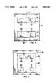
- FIG. 1 illustrates how components were mounted to a circuit board in the past
- FIG. 2 illustrates a mask footprint for the arrangement of FIG. 1
- FIG. 3 illustrates a component mounted to a circuit board using split conductive pads
- FIG. 4 illustrates a mask footprint for the arrangement of FIG. 3
- FIG. 5 illustrates a mask footprint when conductive paths are not routed beneath the component.
- FIG. 3 illustrates component 50 with conductive terminals 52 and 54.
- Component 50 is mounted to top surface 56 of circuit board 58.
- Conductive terminal 52 is attached to split conductive pad portion 60 and split conductive pad portion 61.
- Conductive terminal 54 is attached to split conductive pad portions 62 and 63.
- the conductive terminals are attached to the split conductive pad portions by solder 64. To facilitate this connection, it is preferable to tin plate the surfaces that will be contacting the solder.
- Top surface 56 of circuit board 58 is protected by nonconductive mask 66. Nonconductive mask 66 does not cover the split conductive pad portions or the areas immediately surrounding those portions.
- the present invention provides pathways 68 and 69 in addition to pathway 70, and thereby facilitates cleaning debris from beneath component 50.
- Pathway 68 is formed by the space between conductive pad portions 60 and 61
- pathway 69 is formed by the space between conductive pad portions 62 and 63.
- FIG. 4 illustrates a mask footprint for the arrangement shown in FIG. 3.
- Areas 80 and 82 indicate the portions of top surface 56 which are not covered by mask 66.
- Split conductive pad portions 60, 61, 62, and 63 are not covered by mask 66.
- conductive pad portions should be spaced apart at a maximum distance. Maximizing the spacing enlarges the area through which the cleaning solution and debris can flow. It is preferable to maximize the spacing between the conductive pad portions by positioning each conductive pad portion so that it attaches to the outer portion of the component's conductive terminal.
- FIG. 5 illustrates a mask footprint where mask 66 does not cover the area under component 50.
- Area 90 indicates the portion of top surface 56 which is not covered by mask 66.
- the uncovered area included conductive pad portions 60, 61, 62 and 63.
Landscapes
- Engineering & Computer Science (AREA)
- Microelectronics & Electronic Packaging (AREA)
- Manufacturing & Machinery (AREA)
- Manufacturing Of Printed Wiring (AREA)
- Electric Connection Of Electric Components To Printed Circuits (AREA)
Abstract
A component is mounted to a circuit board using two spaced apart conductive pad portions that make electrical contact with a terminal of the component. The space between the conductive pad portions provides an additional path through which a cleaning solution and debris can flow.
Description
This application is a continuation of application Ser. No. 07/875,887, filed Apr. 29, 1992, now abandoned.
1. Field of the Invention
The present invention relates to circuit boards, more specifically it relates to mounting components on a circuit board.
2. Description of the Related Art
Typically, the surface of a circuit board contains conductive paths and conductive pads. The conductive pads are used to connect a component to a conductive path which may be on an outer or inner surface of the circuit board. The outer surface of the circuit board is protected by a mask of nonconductive material. This mask usually covers the entire top surface of the circuit board except for the pads. The pads are left uncovered to permit soldering components to the pads.
FIG. 1 illustrates component 10, with conductive contacts 12 and 14, mounted to circuit board 16. Contact 12 is connected to pad 18 by solder 22 and contact 14 is connected to pad 20 by solder 24. Upper surface 26 of circuit board 16 is protected by mask 28. Mask 28 covers all of surface 26 except for the areas including and surrounding pads 18 and 20. Pads 18 and 20 are left uncovered so that electrical contact can be made with the conductive contacts of component 10.
FIG. 2 is a top view of circuit board 16 illustrating the areas not covered by mask 28. Areas 36 and 38 are the portions of upper surface 26 that are not covered by mask 28. Area 36 leaves pad 18 and a small portion of top surface 26 uncovered. Area 38 leaves pad 20 and a small portion of surface 26 uncovered.
Referring to FIG. 1, this component mounting technique results in space 44, which is the space between the top surface of mask 28 and the bottom surface of component 10, being rather small. A typical height for space 44 is approximately 0.002 inches.
During the manufacturing process, it is typical for solder flux and other residue to become trapped in space 44. In the past, this debris was removed by cleaning the assembled circuit board using CFCs. It has been learned that CFCs damage the earth's ozone layer, and therefore it is no longer desirable to use such a substance to remove the debris from space 44.
Water is one of the more desirable substitutes for a CFC cleaning solution. Unfortunately, water does not remove debris from space 44 as thoroughly as CFCs. Therefore, it is desirable to mount components to a circuit board in a fashion that allows thorough cleaning using water.
The present invention provides a split conductive pad to which a component conductive terminal can be mounted so that an electrical connection is provided between the component and a circuit board on which the split conductive pad is located. The split conductive pad comprises a first and a second conductive portion. The first and second conductive portions are spaced apart so that the component's conductive terminal can be in simultaneous attachment with each conductive portion.
The present invention provides additional paths through which a cleaning solution can flow and thereby facilitates removing debris from beneath the component. The additional paths enable thorough cleaning with water or other alternate cleaning solutions rather than a CFC solution, and thereby eliminates the need for using CFCs to remove debris from underneath components on circuit boards.
FIG. 1 illustrates how components were mounted to a circuit board in the past;
FIG. 2 illustrates a mask footprint for the arrangement of FIG. 1;
FIG. 3 illustrates a component mounted to a circuit board using split conductive pads;
FIG. 4 illustrates a mask footprint for the arrangement of FIG. 3; and
FIG. 5 illustrates a mask footprint when conductive paths are not routed beneath the component.
FIG. 3 illustrates component 50 with conductive terminals 52 and 54. Component 50 is mounted to top surface 56 of circuit board 58. Conductive terminal 52 is attached to split conductive pad portion 60 and split conductive pad portion 61. Conductive terminal 54 is attached to split conductive pad portions 62 and 63. The conductive terminals are attached to the split conductive pad portions by solder 64. To facilitate this connection, it is preferable to tin plate the surfaces that will be contacting the solder. Top surface 56 of circuit board 58 is protected by nonconductive mask 66. Nonconductive mask 66 does not cover the split conductive pad portions or the areas immediately surrounding those portions.
The present invention provides pathways 68 and 69 in addition to pathway 70, and thereby facilitates cleaning debris from beneath component 50. Pathway 68 is formed by the space between conductive pad portions 60 and 61, and pathway 69 is formed by the space between conductive pad portions 62 and 63.
FIG. 4 illustrates a mask footprint for the arrangement shown in FIG. 3. Areas 80 and 82 indicate the portions of top surface 56 which are not covered by mask 66. Split conductive pad portions 60, 61, 62, and 63 are not covered by mask 66.
The flow of cleaning solution and debris is facilitated by keeping the space between the conductive pad portions unobstructed. To further facilitate the flow, conductive pad portions should be spaced apart at a maximum distance. Maximizing the spacing enlarges the area through which the cleaning solution and debris can flow. It is preferable to maximize the spacing between the conductive pad portions by positioning each conductive pad portion so that it attaches to the outer portion of the component's conductive terminal.
The flow of the cleaning solution and debris is further facilitated by eliminating mask 66 from the area beneath component 50. Mask 66 is not needed beneath component 50 when conductive paths are not routed under the component. The height of the space beneath component 50 is increased by not covering this area with mask 66, and thereby facilitates the flow of the cleaning solution and debris. FIG. 5 illustrates a mask footprint where mask 66 does not cover the area under component 50. Area 90 indicates the portion of top surface 56 which is not covered by mask 66. The uncovered area included conductive pad portions 60, 61, 62 and 63.
It is preferable to use between approximately 0.5 ounces of copper per square inch and approximately 3 ounces of copper per square inch for each conductive pad portion. It is more preferable to use approximately 1.5 ounces of copper per square inch.
Claims (4)
1. A split conductive pad electrically connected to a conductive terminal of a component and thus electrically connected to a single conductive path of a circuit board, said conductive pad comprising a first raised conductive portion, said first raised portion having a first top surface and a first bottom surface and a second raised conductive portion, said second raised portion having a second top surface and a second bottom surface wherein said first and second bottom surfaces are electrically connected to said conductive path in a way that said first conductive portion and said second conductive portion are physically separated and raised above the surface of said conductive path so that said conductive terminal is in simultaneous connection with said first top surface and said second top surface.
2. A split conductor pad assembly to facilitate the cleaning of an assembled circuit board comprising:
a) a component having a first conductive terminal and a second conductive terminal;
b) a circuit board having a first conductive path and a second conductive path;
c) a first split conductive pad comprising a first conductive portion and a second conductive portion wherein both first and second conductive portions are electrically connected to said first conductive path in such a manner that said first and second conductive portions do not abut;
d) a second split conductive pad comprising a third conductive portion and a fourth conductive portion wherein both third and fourth conductive portions are electrically connected to said second conductive path in such a manner that said third and forth conductive portions do not abut;
e) connecting means for electrically connecting said first conductive terminal atop said first and second conductive portions;
f) connecting means for electrically connecting said second conductive terminal atop said third and fourth conductive portions; and
g) a plurality of pathways defined between said component and said circuit board;
whereby said pathways provide a means in which a cleaning solution can flow between said component and said circuit board.
3. The semiconductor assembly of claim 2 wherein said connecting means is solder.
4. The semiconductor assembly of claim 2 wherein said cleaning solution is water.
Priority Applications (1)
| Application Number | Priority Date | Filing Date | Title |
|---|---|---|---|
| US08/191,051 US5425647A (en) | 1992-04-29 | 1994-02-02 | Split conductive pad for mounting components to a circuit board |
Applications Claiming Priority (2)
| Application Number | Priority Date | Filing Date | Title |
|---|---|---|---|
| US87588792A | 1992-04-29 | 1992-04-29 | |
| US08/191,051 US5425647A (en) | 1992-04-29 | 1994-02-02 | Split conductive pad for mounting components to a circuit board |
Related Parent Applications (1)
| Application Number | Title | Priority Date | Filing Date |
|---|---|---|---|
| US87588792A Continuation | 1992-04-29 | 1992-04-29 |
Publications (1)
| Publication Number | Publication Date |
|---|---|
| US5425647A true US5425647A (en) | 1995-06-20 |
Family
ID=25366544
Family Applications (1)
| Application Number | Title | Priority Date | Filing Date |
|---|---|---|---|
| US08/191,051 Expired - Fee Related US5425647A (en) | 1992-04-29 | 1994-02-02 | Split conductive pad for mounting components to a circuit board |
Country Status (1)
| Country | Link |
|---|---|
| US (1) | US5425647A (en) |
Cited By (19)
| Publication number | Priority date | Publication date | Assignee | Title |
|---|---|---|---|---|
| US5731960A (en) * | 1996-09-19 | 1998-03-24 | Bay Networks, Inc. | Low inductance decoupling capacitor arrangement |
| US5943217A (en) * | 1994-05-06 | 1999-08-24 | Seiko Epson Corporation | Printed circuit board for mounting at least one electronic part |
| US6169253B1 (en) * | 1998-06-08 | 2001-01-02 | Visteon Global Technologies, Inc. | Solder resist window configurations for solder paste overprinting |
| US6324066B1 (en) * | 1999-07-19 | 2001-11-27 | Motorola, Inc. | Surface mountable electronic device |
| US6515572B2 (en) * | 1997-08-23 | 2003-02-04 | Koninklijke Philips Electronics N.V. | Circuit arrangement comprising an SMD-component, in particular a temperature sensor, and a method of manufacturing a temperature sensor |
| US6657133B1 (en) * | 2001-05-15 | 2003-12-02 | Xilinx, Inc. | Ball grid array chip capacitor structure |
| US20050082682A1 (en) * | 2003-10-21 | 2005-04-21 | Advanced Semiconductor Engineering, Inc. | Prevention of contamination on bonding pads of wafer during SMT |
| WO2005052527A1 (en) * | 2003-11-28 | 2005-06-09 | Zitzmann, Heinrich | Component and method for the production thereof |
| EP1593450A1 (en) | 2004-05-04 | 2005-11-09 | Agere System Inc. | Electronic device with surface mount components having stand-off space free of solder mask under the component - method for manfacturing the same |
| US20060231124A1 (en) * | 2002-07-16 | 2006-10-19 | Chemical Art Technology Inc. | Substrate processing method |
| US20070044998A1 (en) * | 2005-08-26 | 2007-03-01 | Chan Aik H | Electronic package and circuit board having segmented contact pads |
| US20070125573A1 (en) * | 2005-07-22 | 2007-06-07 | Hon Hai Precision Industry Co., Ltd. | Printed circuit board |
| US20080202804A1 (en) * | 2007-02-26 | 2008-08-28 | Yasuhiro Fakutomi | Printed circuit board and method of producing the same |
| CN100442949C (en) * | 2004-09-24 | 2008-12-10 | 松下电器产业株式会社 | Circuit component mounting device |
| US20100177491A1 (en) * | 2009-01-12 | 2010-07-15 | Alcatel-Lucent Usa Inc. | Orientation-tolerant land pattern and method of manufacturing the same |
| US20110068743A1 (en) * | 2008-05-29 | 2011-03-24 | Kyocera Corporation | Terminal component and portable electronic device |
| CN102907187A (en) * | 2010-05-26 | 2013-01-30 | 株式会社村田制作所 | Substrate with built-in component |
| US20130286644A1 (en) * | 2012-04-25 | 2013-10-31 | Hon Hai Precision Industry Co., Ltd. | Led light bar with balanced resistance for light emtitting diodes thereof |
| US8742598B2 (en) * | 2011-10-05 | 2014-06-03 | Infineon Technologies Ag | Semiconductor structure and method for making same |
Citations (7)
| Publication number | Priority date | Publication date | Assignee | Title |
|---|---|---|---|---|
| US3770874A (en) * | 1970-09-08 | 1973-11-06 | Siemens Ag | Contact members for soldering electrical components |
| US3778530A (en) * | 1971-04-01 | 1973-12-11 | W Reimann | Flatpack lead positioning device |
| US4811081A (en) * | 1987-03-23 | 1989-03-07 | Motorola, Inc. | Semiconductor die bonding with conductive adhesive |
| JPH02237091A (en) * | 1989-03-09 | 1990-09-19 | Fujitsu Ltd | Printed wiring board |
| US5089936A (en) * | 1988-09-09 | 1992-02-18 | Hitachi, Ltd. | Semiconductor module |
| US5206795A (en) * | 1991-12-30 | 1993-04-27 | Ag Communication Systems Corporation | Compliant connection for substrates |
| US5249098A (en) * | 1991-08-22 | 1993-09-28 | Lsi Logic Corporation | Semiconductor device package with solder bump electrical connections on an external surface of the package |
-
1994
- 1994-02-02 US US08/191,051 patent/US5425647A/en not_active Expired - Fee Related
Patent Citations (7)
| Publication number | Priority date | Publication date | Assignee | Title |
|---|---|---|---|---|
| US3770874A (en) * | 1970-09-08 | 1973-11-06 | Siemens Ag | Contact members for soldering electrical components |
| US3778530A (en) * | 1971-04-01 | 1973-12-11 | W Reimann | Flatpack lead positioning device |
| US4811081A (en) * | 1987-03-23 | 1989-03-07 | Motorola, Inc. | Semiconductor die bonding with conductive adhesive |
| US5089936A (en) * | 1988-09-09 | 1992-02-18 | Hitachi, Ltd. | Semiconductor module |
| JPH02237091A (en) * | 1989-03-09 | 1990-09-19 | Fujitsu Ltd | Printed wiring board |
| US5249098A (en) * | 1991-08-22 | 1993-09-28 | Lsi Logic Corporation | Semiconductor device package with solder bump electrical connections on an external surface of the package |
| US5206795A (en) * | 1991-12-30 | 1993-04-27 | Ag Communication Systems Corporation | Compliant connection for substrates |
Cited By (27)
| Publication number | Priority date | Publication date | Assignee | Title |
|---|---|---|---|---|
| US5943217A (en) * | 1994-05-06 | 1999-08-24 | Seiko Epson Corporation | Printed circuit board for mounting at least one electronic part |
| US6201193B1 (en) | 1994-05-06 | 2001-03-13 | Seiko Epson Corporation | Printed circuit board having a positioning marks for mounting at least one electronic part |
| US5731960A (en) * | 1996-09-19 | 1998-03-24 | Bay Networks, Inc. | Low inductance decoupling capacitor arrangement |
| US6515572B2 (en) * | 1997-08-23 | 2003-02-04 | Koninklijke Philips Electronics N.V. | Circuit arrangement comprising an SMD-component, in particular a temperature sensor, and a method of manufacturing a temperature sensor |
| US6169253B1 (en) * | 1998-06-08 | 2001-01-02 | Visteon Global Technologies, Inc. | Solder resist window configurations for solder paste overprinting |
| US6324066B1 (en) * | 1999-07-19 | 2001-11-27 | Motorola, Inc. | Surface mountable electronic device |
| US6657133B1 (en) * | 2001-05-15 | 2003-12-02 | Xilinx, Inc. | Ball grid array chip capacitor structure |
| US20060231124A1 (en) * | 2002-07-16 | 2006-10-19 | Chemical Art Technology Inc. | Substrate processing method |
| US20050082682A1 (en) * | 2003-10-21 | 2005-04-21 | Advanced Semiconductor Engineering, Inc. | Prevention of contamination on bonding pads of wafer during SMT |
| US7245011B2 (en) * | 2003-10-21 | 2007-07-17 | Advanced Semiconductor Engineering, Inc. | Prevention of contamination on bonding pads of wafer during SMT |
| US7537963B2 (en) | 2003-11-28 | 2009-05-26 | Georg Bernitz | Device and method for manufacturing the same |
| WO2005052527A1 (en) * | 2003-11-28 | 2005-06-09 | Zitzmann, Heinrich | Component and method for the production thereof |
| US20080041620A1 (en) * | 2004-05-04 | 2008-02-21 | Albanese Patricia M | Surface mount attachment of components |
| EP1593450A1 (en) | 2004-05-04 | 2005-11-09 | Agere System Inc. | Electronic device with surface mount components having stand-off space free of solder mask under the component - method for manfacturing the same |
| CN100442949C (en) * | 2004-09-24 | 2008-12-10 | 松下电器产业株式会社 | Circuit component mounting device |
| US7572983B2 (en) | 2005-07-22 | 2009-08-11 | Hong Fu Jin Precision Industry (Shenzhen) Co., Ltd. | Printed circuit board |
| US20070125573A1 (en) * | 2005-07-22 | 2007-06-07 | Hon Hai Precision Industry Co., Ltd. | Printed circuit board |
| US7280370B2 (en) * | 2005-08-26 | 2007-10-09 | Delphi Technologies, Inc. | Electronic package and circuit board having segmented contact pads |
| US20070044998A1 (en) * | 2005-08-26 | 2007-03-01 | Chan Aik H | Electronic package and circuit board having segmented contact pads |
| US20080202804A1 (en) * | 2007-02-26 | 2008-08-28 | Yasuhiro Fakutomi | Printed circuit board and method of producing the same |
| US20110068743A1 (en) * | 2008-05-29 | 2011-03-24 | Kyocera Corporation | Terminal component and portable electronic device |
| US8602830B2 (en) * | 2008-05-29 | 2013-12-10 | Kyocera Corporation | Terminal component and portable electronic device |
| US20100177491A1 (en) * | 2009-01-12 | 2010-07-15 | Alcatel-Lucent Usa Inc. | Orientation-tolerant land pattern and method of manufacturing the same |
| US8094460B2 (en) * | 2009-01-12 | 2012-01-10 | Alcatel Lucent | Orientation-tolerant land pattern and method of manufacturing the same |
| CN102907187A (en) * | 2010-05-26 | 2013-01-30 | 株式会社村田制作所 | Substrate with built-in component |
| US8742598B2 (en) * | 2011-10-05 | 2014-06-03 | Infineon Technologies Ag | Semiconductor structure and method for making same |
| US20130286644A1 (en) * | 2012-04-25 | 2013-10-31 | Hon Hai Precision Industry Co., Ltd. | Led light bar with balanced resistance for light emtitting diodes thereof |
Similar Documents
| Publication | Publication Date | Title |
|---|---|---|
| US5425647A (en) | Split conductive pad for mounting components to a circuit board | |
| US4642889A (en) | Compliant interconnection and method therefor | |
| AU544844B2 (en) | Method of mounting interrelated components | |
| RU99120781A (en) | MODULE FOR A CHIP CARD AND METHOD FOR ITS MANUFACTURE, AND ALSO A CHIP CARD, INCLUDING SUCH A MODULE | |
| CA1201820A (en) | Semiconductor integrated circuit including a lead frame chip support | |
| EP0551382A4 (en) | Semiconductor chip assemblies, methods of making same and components for same | |
| JPH09214097A (en) | Printed circuit board | |
| GB2127217A (en) | Semiconductor chip carriers and housings | |
| KR890007939Y1 (en) | Printed circuit board support structure | |
| EP0711107A2 (en) | Control circuit arrangement | |
| EP0183724A1 (en) | Integrated circuit package. | |
| KR890004204B1 (en) | Filtration splicer | |
| US4470648A (en) | Interconnection construction to thick film substrate | |
| US4868980A (en) | Method of designing and manufacturing circuits using universal circuit board | |
| GB2202682A (en) | Connection leads for surface mounted components | |
| US4791722A (en) | Method of designing and manufacturing circuits using universal circuit board | |
| US5502278A (en) | Encased electronic circuit with chip on a grid zone of conductive contacts | |
| US5163605A (en) | Method for mounting components to a circuit board | |
| US6833512B2 (en) | Substrate board structure | |
| EP0942635B1 (en) | A power semiconductor device for "flip-chip" connections | |
| JP4278777B2 (en) | Electrical connector | |
| JPH0220847Y2 (en) | ||
| JP3896613B2 (en) | Electronic equipment | |
| JPH0519974Y2 (en) | ||
| RU2168798C2 (en) | Semiconductor device and its manufacturing process |
Legal Events
| Date | Code | Title | Description |
|---|---|---|---|
| REMI | Maintenance fee reminder mailed | ||
| LAPS | Lapse for failure to pay maintenance fees | ||
| FP | Expired due to failure to pay maintenance fee |
Effective date: 19990620 |
|
| STCH | Information on status: patent discontinuation |
Free format text: PATENT EXPIRED DUE TO NONPAYMENT OF MAINTENANCE FEES UNDER 37 CFR 1.362 |