US5409743A - PECVD process for forming BPSG with low flow temperature - Google Patents

PECVD process for forming BPSG with low flow temperature Download PDF

Info

Publication number
US5409743A
US5409743A US08/062,658 US6265893A US5409743A US 5409743 A US5409743 A US 5409743A US 6265893 A US6265893 A US 6265893A US 5409743 A US5409743 A US 5409743A
Authority
US
United States
Prior art keywords
recited
reactants
forming
film
bpsg
Prior art date
Legal status (The legal status is an assumption and is not a legal conclusion. Google has not performed a legal analysis and makes no representation as to the accuracy of the status listed.)
Expired - Fee Related
Application number
US08/062,658
Inventor
Mark D. Bouffard
William J. King
Cheryl M. Martin
Current Assignee (The listed assignees may be inaccurate. Google has not performed a legal analysis and makes no representation or warranty as to the accuracy of the list.)
International Business Machines Corp
Original Assignee
International Business Machines Corp
Priority date (The priority date is an assumption and is not a legal conclusion. Google has not performed a legal analysis and makes no representation as to the accuracy of the date listed.)
Filing date
Publication date
Application filed by International Business Machines Corp filed Critical International Business Machines Corp
Priority to US08/062,658 priority Critical patent/US5409743A/en
Assigned to INTERNATIONAL BUSINESS MACHINES CORPORATION reassignment INTERNATIONAL BUSINESS MACHINES CORPORATION ASSIGNMENT OF ASSIGNORS INTEREST (SEE DOCUMENT FOR DETAILS). Assignors: MARTIN, CHERYL M., BOUFFARD, MARK D., KING, WILLIAM J.
Priority to JP6050073A priority patent/JP2710551B2/en
Priority to EP94106390A priority patent/EP0624660A1/en
Application granted granted Critical
Publication of US5409743A publication Critical patent/US5409743A/en
Anticipated expiration legal-status Critical
Expired - Fee Related legal-status Critical Current

Links

Images

Classifications

    • H10P14/6923
    • CCHEMISTRY; METALLURGY
    • C23COATING METALLIC MATERIAL; COATING MATERIAL WITH METALLIC MATERIAL; CHEMICAL SURFACE TREATMENT; DIFFUSION TREATMENT OF METALLIC MATERIAL; COATING BY VACUUM EVAPORATION, BY SPUTTERING, BY ION IMPLANTATION OR BY CHEMICAL VAPOUR DEPOSITION, IN GENERAL; INHIBITING CORROSION OF METALLIC MATERIAL OR INCRUSTATION IN GENERAL
    • C23CCOATING METALLIC MATERIAL; COATING MATERIAL WITH METALLIC MATERIAL; SURFACE TREATMENT OF METALLIC MATERIAL BY DIFFUSION INTO THE SURFACE, BY CHEMICAL CONVERSION OR SUBSTITUTION; COATING BY VACUUM EVAPORATION, BY SPUTTERING, BY ION IMPLANTATION OR BY CHEMICAL VAPOUR DEPOSITION, IN GENERAL
    • C23C16/00Chemical coating by decomposition of gaseous compounds, without leaving reaction products of surface material in the coating, i.e. chemical vapour deposition [CVD] processes
    • C23C16/22Chemical coating by decomposition of gaseous compounds, without leaving reaction products of surface material in the coating, i.e. chemical vapour deposition [CVD] processes characterised by the deposition of inorganic material, other than metallic material
    • C23C16/30Deposition of compounds, mixtures or solid solutions, e.g. borides, carbides, nitrides
    • C23C16/40Oxides
    • C23C16/401Oxides containing silicon
    • CCHEMISTRY; METALLURGY
    • C23COATING METALLIC MATERIAL; COATING MATERIAL WITH METALLIC MATERIAL; CHEMICAL SURFACE TREATMENT; DIFFUSION TREATMENT OF METALLIC MATERIAL; COATING BY VACUUM EVAPORATION, BY SPUTTERING, BY ION IMPLANTATION OR BY CHEMICAL VAPOUR DEPOSITION, IN GENERAL; INHIBITING CORROSION OF METALLIC MATERIAL OR INCRUSTATION IN GENERAL
    • C23CCOATING METALLIC MATERIAL; COATING MATERIAL WITH METALLIC MATERIAL; SURFACE TREATMENT OF METALLIC MATERIAL BY DIFFUSION INTO THE SURFACE, BY CHEMICAL CONVERSION OR SUBSTITUTION; COATING BY VACUUM EVAPORATION, BY SPUTTERING, BY ION IMPLANTATION OR BY CHEMICAL VAPOUR DEPOSITION, IN GENERAL
    • C23C16/00Chemical coating by decomposition of gaseous compounds, without leaving reaction products of surface material in the coating, i.e. chemical vapour deposition [CVD] processes
    • C23C16/56After-treatment
    • H10P14/6336

Definitions

  • This invention generally relates to smoothing contours on the surface of an integrated circuit chip by flowing a borophosphosilicate glass (BPSG). More particularly, it relates to a composition of the BPSG and methods for its deposition and anneal that provide desired step coverage, wall angle, and film stability. Even more particularly, it relates to a plasma enhanced chemical vapor deposition (PECVD) process for BPSG deposition that provides a BPSG composition that can later be flowed at low temperature in a non-oxidizing environment.
  • PECVD plasma enhanced chemical vapor deposition
  • BPSG films are widely used in the semiconductor industry, offering an insulating material with two key advantages: (1) BPSG can be flowed at a lower temperature than other materials to smooth steps and fill trenches, providing a gradually tapered contour that permits deposition of a uniform thickness of metal; and (2) the phosphorous in BPSG is capable of mobile ion gettering.
  • the ability to process at low temperature is increasingly important for the fabrication of integrated circuits with devices having short channel lengths and shallow junctions.
  • a smoother surface is achieved without redistribution of dopants in these underlying integrated circuit devices.
  • a surface free of sharply changing topology permits metal layers to be deposited with more uniform metal thickness and provides a more reliable insulation between conductive layers. Without a material that flows, it was found that the insulator and the conductor are much thinner adjacent steps, and these are the regions that are later found to produce either opens in the metal lines or short circuits between levels of metal.
  • a BPSG anneal step that flows the glass eliminates the thinning problems and increases chip reliability.
  • Chemical vapor deposition has long been used to deposit BPSG on integrated circuits.
  • Three processes are available, atmospheric pressure chemical vapor deposition (APCVD), low pressure chemical vapor deposition (LPCVD), and plasma enhanced chemical vapor deposition (PECVD).
  • APCVD atmospheric pressure chemical vapor deposition
  • LPCVD low pressure chemical vapor deposition
  • PECVD plasma enhanced chemical vapor deposition
  • APCVD APCVD
  • wafers move on a belt through a furnace at elevated temperature under injectors that provide separate flows of reactant gases that mix and react on the wafer surface.
  • Reactant gases typically emanate from different parts of the injector and reactants are held apart from each other for a short distance in the furnace by nitrogen blankets so that reactants mix and react only when they reach the wafer surface.
  • Gases such as silane, oxygen, diborane, and phosphene are used as reactants.
  • the process provides BPSG films that flow at low temperature.
  • the BPSG films formed by APCVD flow at temperatures below 1000° C. in a non-oxidizing environment.
  • the APCVD process poses significant manufacturing difficulties, including: (1) a high level of particulates on each wafer; (2) film thickness and film compositional variation within a wafer and between wafers; (3) the requirement for frequent injector replacement for cleaning, and the additional substantial tool down-time for requisite performance tests after injector replacement; and (4) the inability to quickly switch from BPSG deposition to another material deposition without changing injectors.
  • a process providing fewer defects, improved thickness and compositional uniformity, self cleaning of reactor parts, and the ability to switch the materials being deposited without changing reactor parts would therefore provide significant advantages to a manufacturer.
  • a process for depositing BPSG using PECVD has posed significant difficulties as reported by Tong et. al. in "Solid State Technology," January, 1984, p. 161-170 and by Kern and Smeltzer in “Solid State Technology,” June, 1985, p. 171-179.
  • One of the difficulties noted was that the PECVD film needed a 70° higher anneal temperature to achieve the same wall angle when the anneal was conducted in a dry nitrogen environment than when it was conducted in a steam environment.
  • the article also points out that annealing in a steam environment can cause problems for exposed contact openings, namely the growth of oxide in the contacts.
  • means are provided in a second embodiment of the invention to take advantage of the fact that a film with a high P 2 O 3 composition does not flow during a non-oxidizing anneal required immediately after deposition.
  • the flow step is delayed until after contact openings through the BPSG are formed.
  • an oxidizing environment such as oxygen or steam is used in an anneal step, converting the P 2 O 3 to P 2 O 5 which flows, and reshapes contact openings so they have more sloping sidewalls.
  • means are provided to control the wall angle of a BPSG film by controlling the P 2 O 3 /P 2 O 5 ratio in the film.
  • FIG. 1a is a cross-sectional view of a BPSG covered step that has not flowed
  • FIG. 1b is a cross-sectional view of a BPSG covered step that has flowed
  • FIG. 2 is a table showing the P 2 O 3 /P 2 O 5 ratio as a function of process variables
  • FIGS. 4a, 4b and 4c are cross-sectional views showing the process steps for forming a contact with more sloping sidewalls.
  • FIGS. 1a-1b illustrate a semiconducting wafer 18, typically formed from a material such as silicon, on which is formed an integrated circuit array, one cell 20 of which is shown.
  • sharp steps 22 are formed for structures such as gates and other conducting lines.
  • a BPSG film 24a is deposited, usually with a thickness in the range 2000 to 10,000 ⁇ . More preferably, the film thickness is in the range of about 4000 to 8000 ⁇ . Most preferably, about 5300 ⁇ .
  • As-deposited BPSG film 24a is then annealed to smooth contours over step 22 and provide a 1.5 protective layer for the integrated circuit. The result is BPSG film 24b shown in FIG. 1b.
  • the surface of flowed BPSG layer 24b need not be flat; flow is satisfactory if it reduces the wall angle ⁇ b of contour 27b crossing step 22 compared to the wall angle ⁇ a of contour 27a associated with as deposited BPSG film 24a.
  • deposited BPSG layer 24a has wall angle ⁇ a in the range of 50° to 60° and flowed BPSG layer 24b has wall angle ⁇ b in the range of 25° to 40°.
  • PECVD was found to have a distinct disadvantage compared to APCVD.
  • the BPSG required a 70° higher flow temperature to achieve comparable contours when the anneal was conducted in a non-oxidizing environment, such as dry nitrogen than when conducted in a steam environment.
  • the increased resistivity arises because boron-doped silicon located in the source and drain regions of transistors is oxidized when oxygen diffuses through the BPSG to the silicon surface. Boron preferentially segregates into the silicon oxide, leaving less boron in the silicon to provide mobile carriers. While a silicon nitride layer formed before the BPSG deposition could be used to prevent the silicon oxidation and thereby avoid the boron segregation, the addition of a nitride layer would add to cost and process complexity.
  • the present inventors have determined that increasing the proportion of P 2 O 3 to P 2 O 5 in the composition inhibits glass flow in a non-oxidizing environment and raises the flow temperature.
  • the present inventors believe that when a film with a large amount of P 2 O 5 is annealed in an oxidizing environment, the satisfactory low temperature flow results are accounted for by the fact that some of the P 2 O 3 is first further oxidized to P 2 O 5 .
  • the conditions providing a reduced flow temperature while retaining film stability are those that provide a P 2 O 3 /P 2 O 5 ratio of no lower than about 2% and no higher than about 25%.
  • wall angle ⁇ b illustrated in FIG. 1b can be controlled by controlling the anneal temperature.
  • the present inventors have determined that for a given anneal temperature, wall angle ⁇ b can be controlled by controlling the ratio of P 2 O 3 /P 2 O 5 by methods described hereinbelow.
  • Sources of silicon include silane and tetraethylorthosilicate (TEOS).
  • Sources of oxygen include nitrous oxide and oxygen.
  • Sources of phosphorous include phosphene, trimethylphosphate (TMP), and triethylphosphate (TEP),
  • Sources of boron include diborane and trimethylborate (TMB).
  • FIG. 2 sets forth experimental data showing the effect of three process variables, N 2 O flow, SiH 4 flow, and system pressure, on the ratio of P 2 O 3 /P 2 O 5 in BPSG layers deposited with a Novellus PECVD tool. Also shown is the effect of these parameters on film thickness and the amount of boron and phosphorous incorporated in the film.
  • wafers pass through a load lock into a reaction chamber on a heated block that serves as the bottom electrode of a pair of parallel plates.
  • the top electrode includes a showerhead through which the premixed reactants pass.
  • diborane was diluted with nitrogen in a 10:1 ratio and the mixture flowed at 450 ccpm.
  • Phosphene had the same dilution and flowed at 200 ccpm.
  • the silane flow shown in Table 1 is before a 5:1 dilution with nitrogen. Nitrous oxide was not diluted. Temperature was fixed at 400° C. and the electrodes were connected to a 13.56 MHz power supply that was set at 1000 Watts to form the plasma in the gas mixture. In each case the reaction proceeded for 1 minute. Boron and phosphorus weight percent were measured using Inductively Coupled Argon Plasma Optical Emission Spectroscopy (ICAP). BPSG thickness and range were measured with a spectrophotometer. Ion chromatography was used to measure the percent P 2 O 3 /P 2 O 5 .
  • ICAP Inductively Coupled Argon Plasma Optical Emission Spectroscopy
  • Preferred nitrous oxide flow is in the range of 3 to 10 lpm, the 6 to 10 lpm range is more preferred, and 8 to 10 lpm is most preferred.
  • Preferred deposition temperature is in the range of about 250° to about 500° C., more preferably about 400° C.
  • Preferred system power is in the range of about 500 to about 1500 Watts, more preferably about 1000 Watts.
  • FIGS. 4a-4c An embodiment of the invention further utilizing the ability to control flow temperature and flow angle by controlling the P 2 O 3 /P 2 O 5 ratio is illustrated in FIGS. 4a-4c.
  • This embodiment provides sloping sidewalls in contact holes without the need for wet etch or complex dry etch processing.
  • the sloping sidewalls are necessary to maintain metal thickness uniformity when deposited into contact vias.
  • BPSG layer 24a is deposited using PECVD with a high P 2 O 3 /P 2 O 5 ratio, e.g., about 20%, by method described herein-above and annealed at 900° C. in a dry nitrogen environment, which anneal does not substantially flow BPSG layer 24a.
  • contact openings 40 are formed in BPSG layer 24a by photolithographic and reactive ion etch process known in the art, producing substantially perpendicular sidewalls 42a.
  • wafer 18 is annealed in an oxygen environment, and the BPSG film flows to form BPSG layer 24c with more sloping sidewalls 42b in contact openings 40.

Landscapes

  • Chemical & Material Sciences (AREA)
  • General Chemical & Material Sciences (AREA)
  • Chemical Kinetics & Catalysis (AREA)
  • Engineering & Computer Science (AREA)
  • Materials Engineering (AREA)
  • Mechanical Engineering (AREA)
  • Metallurgy (AREA)
  • Organic Chemistry (AREA)
  • Inorganic Chemistry (AREA)
  • Formation Of Insulating Films (AREA)
  • Chemical Vapour Deposition (AREA)

Abstract

A method of forming a BPSG film in a PECVD reactor with ratios of P2 O3 /P2 O5 such that the film flows at low temperature in a non-oxidizing ambient and produces a reduced number of particulates. The method permits tailoring of the wall angle of a BPSG film by controlling the P2 O3 /P2 O5 ratio.

Description

FIELD OF THE INVENTION
This invention generally relates to smoothing contours on the surface of an integrated circuit chip by flowing a borophosphosilicate glass (BPSG). More particularly, it relates to a composition of the BPSG and methods for its deposition and anneal that provide desired step coverage, wall angle, and film stability. Even more particularly, it relates to a plasma enhanced chemical vapor deposition (PECVD) process for BPSG deposition that provides a BPSG composition that can later be flowed at low temperature in a non-oxidizing environment.
BACKGROUND OF THE INVENTION
BPSG films are widely used in the semiconductor industry, offering an insulating material with two key advantages: (1) BPSG can be flowed at a lower temperature than other materials to smooth steps and fill trenches, providing a gradually tapered contour that permits deposition of a uniform thickness of metal; and (2) the phosphorous in BPSG is capable of mobile ion gettering.
The ability to process at low temperature is increasingly important for the fabrication of integrated circuits with devices having short channel lengths and shallow junctions. By taking advantage of the ability to flow the glass at low temperature, a smoother surface is achieved without redistribution of dopants in these underlying integrated circuit devices. A surface free of sharply changing topology permits metal layers to be deposited with more uniform metal thickness and provides a more reliable insulation between conductive layers. Without a material that flows, it was found that the insulator and the conductor are much thinner adjacent steps, and these are the regions that are later found to produce either opens in the metal lines or short circuits between levels of metal. A BPSG anneal step that flows the glass eliminates the thinning problems and increases chip reliability.
Chemical vapor deposition (CVD) has long been used to deposit BPSG on integrated circuits. Three processes are available, atmospheric pressure chemical vapor deposition (APCVD), low pressure chemical vapor deposition (LPCVD), and plasma enhanced chemical vapor deposition (PECVD).
In the APCVD process used in manufacturing, wafers move on a belt through a furnace at elevated temperature under injectors that provide separate flows of reactant gases that mix and react on the wafer surface. Reactant gases typically emanate from different parts of the injector and reactants are held apart from each other for a short distance in the furnace by nitrogen blankets so that reactants mix and react only when they reach the wafer surface. Gases such as silane, oxygen, diborane, and phosphene are used as reactants. The process provides BPSG films that flow at low temperature. In particular, the BPSG films formed by APCVD flow at temperatures below 1000° C. in a non-oxidizing environment.
However, the APCVD process poses significant manufacturing difficulties, including: (1) a high level of particulates on each wafer; (2) film thickness and film compositional variation within a wafer and between wafers; (3) the requirement for frequent injector replacement for cleaning, and the additional substantial tool down-time for requisite performance tests after injector replacement; and (4) the inability to quickly switch from BPSG deposition to another material deposition without changing injectors.
A process providing fewer defects, improved thickness and compositional uniformity, self cleaning of reactor parts, and the ability to switch the materials being deposited without changing reactor parts would therefore provide significant advantages to a manufacturer.
A process for depositing BPSG using PECVD has posed significant difficulties as reported by Tong et. al. in "Solid State Technology," January, 1984, p. 161-170 and by Kern and Smeltzer in "Solid State Technology," June, 1985, p. 171-179. One of the difficulties noted was that the PECVD film needed a 70° higher anneal temperature to achieve the same wall angle when the anneal was conducted in a dry nitrogen environment than when it was conducted in a steam environment. The article also points out that annealing in a steam environment can cause problems for exposed contact openings, namely the growth of oxide in the contacts.
Thus, a method is needed to provide BPSG that retains the flow properties of the APCVD process without the disadvantages.
SUMMARY OF THE INVENTION
It is therefore an object of the present invention to provide a PECVD method of forming BPSG films that flow at low temperature in a non-oxidizing environment while providing high resistance to defects.
It is another object of this invention to provide a composition of BPSG formed by PECVD that flows at low temperature in a non-oxidizing environment while providing high resistance to defects.
It is another object of this invention to provide a method of forming contacts with sloping sidewalls using the variable flow characteristics found to be available from the use of PECVD BPSG.
These and other objects of the invention are accomplished by the method more fully described below for forming a BPSG film. According to the invention, it has been found that the higher anneal temperature required of BPSG films formed by means of PECVD is caused by a high proportion of P2 O3 as compared to more fully oxidized P2 O5 in the films; however, a small proportion of P2 O3 is needed in the BPSG film because a purely P2 O5 composition is unstable and produces large quantities of crystalline particulates. Means are provided in the 1.5 invention to achieve a desired proportion of P2 O3 in the film as compared to P2 O5 by adjusting parameters, including silane flow rate, nitrous oxide flow rate, and overall gas pressure during the PECVD deposition.
In addition, means are provided in a second embodiment of the invention to take advantage of the fact that a film with a high P2 O3 composition does not flow during a non-oxidizing anneal required immediately after deposition. In this embodiment the flow step is delayed until after contact openings through the BPSG are formed. Then an oxidizing environment, such as oxygen or steam is used in an anneal step, converting the P2 O3 to P2 O5 which flows, and reshapes contact openings so they have more sloping sidewalls.
In addition means are provided to control the wall angle of a BPSG film by controlling the P2 O3 /P2 O5 ratio in the film.
BRIEF DESCRIPTION OF THE DRAWINGS
The foregoing and other objects, features, and advantages of the invention will be apparent from the following detailed description of the invention, as illustrated in the accompanying drawings, in which:
FIG. 1a is a cross-sectional view of a BPSG covered step that has not flowed;
FIG. 1b is a cross-sectional view of a BPSG covered step that has flowed;
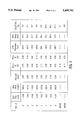
FIG. 2 is a table showing the P2 O3 /P2 O5 ratio as a function of process variables;
FIGS. 3a, 3b and 3c are contour plots showing the P2 O3 /P2 O5 ratio as a function of process variables; and
FIGS. 4a, 4b and 4c are cross-sectional views showing the process steps for forming a contact with more sloping sidewalls.
DETAILED DESCRIPTION OF THE INVENTION
FIGS. 1a-1b illustrate a semiconducting wafer 18, typically formed from a material such as silicon, on which is formed an integrated circuit array, one cell 20 of which is shown. In the course of processing wafer 18, sharp steps 22 are formed for structures such as gates and other conducting lines. A BPSG film 24a is deposited, usually with a thickness in the range 2000 to 10,000Å. More preferably, the film thickness is in the range of about 4000 to 8000Å. Most preferably, about 5300Å. As-deposited BPSG film 24a is then annealed to smooth contours over step 22 and provide a 1.5 protective layer for the integrated circuit. The result is BPSG film 24b shown in FIG. 1b. The surface of flowed BPSG layer 24b need not be flat; flow is satisfactory if it reduces the wall angle Θb of contour 27b crossing step 22 compared to the wall angle Θa of contour 27a associated with as deposited BPSG film 24a. Typically, as deposited BPSG layer 24a has wall angle Θa in the range of 50° to 60° and flowed BPSG layer 24b has wall angle Θb in the range of 25° to 40°.
As noted hereinabove, PECVD was found to have a distinct disadvantage compared to APCVD. With PECVD deposition, the BPSG required a 70° higher flow temperature to achieve comparable contours when the anneal was conducted in a non-oxidizing environment, such as dry nitrogen than when conducted in a steam environment.
However, it was found that smoothing of contours on the surface at lower temperature is achieved by conducting the anneal in an oxidizing environment such as oxygen or steam. But an oxygen environment during the high temperature anneal introduces another problem, namely increased silicide and source-drain resistivity, a problem that decreases the speed of the integrated circuit device.
The increased resistivity arises because boron-doped silicon located in the source and drain regions of transistors is oxidized when oxygen diffuses through the BPSG to the silicon surface. Boron preferentially segregates into the silicon oxide, leaving less boron in the silicon to provide mobile carriers. While a silicon nitride layer formed before the BPSG deposition could be used to prevent the silicon oxidation and thereby avoid the boron segregation, the addition of a nitride layer would add to cost and process complexity.
It is known in the art that two oxidation states are present for the phosphorous in APCVD BPSG films, a P2 O3 state and a more oxidized P2 O5 state. However, it is believed that the prior art has neither taught nor suggested that BPSG film flow properties depend on the ratio of these two oxidation states. And the prior art, as illustrated in Research and Development Note 90-1, "Characteristics of BPSG Films from TEOS Deposited at 500° C." published By Watkins-Johnson Company, March 1990, p. 16, teaches against the finding of the present invention that a portion of P2 O3 is needed for stabilizing the film.
In particular, the present inventors have determined that increasing the proportion of P2 O3 to P2 O5 in the composition inhibits glass flow in a non-oxidizing environment and raises the flow temperature. The present inventors believe that when a film with a large amount of P2 O5 is annealed in an oxidizing environment, the satisfactory low temperature flow results are accounted for by the fact that some of the P2 O3 is first further oxidized to P2 O5. In addition, it has been determined by the present inventors that if the proportion of P2 O3 to P2 O5 is below about 2%, the BPSG film is unstable and a large number of crystalline particulates are formed. Thus, to achieve reduced flow temperature, a proportion of P2 O3 /P2 O5 in the range of 0 to 25% is preferred. However, to enhance film stability, it is preferred that the ratio of P2 O3 /P2 O5 be at least 2%. Thus, for a given boron composition, the conditions providing a reduced flow temperature while retaining film stability are those that provide a P2 O3 /P2 O5 ratio of no lower than about 2% and no higher than about 25%.
It is known in the art that wall angle Θb illustrated in FIG. 1b can be controlled by controlling the anneal temperature. The present inventors have determined that for a given anneal temperature, wall angle Θb can be controlled by controlling the ratio of P2 O3 /P2 O5 by methods described hereinbelow.
Various sources of the silicon, oxygen, phosphorous, and boron are known in the art. Sources of silicon include silane and tetraethylorthosilicate (TEOS). Sources of oxygen include nitrous oxide and oxygen. Sources of phosphorous include phosphene, trimethylphosphate (TMP), and triethylphosphate (TEP), Sources of boron include diborane and trimethylborate (TMB).
FIG. 2 sets forth experimental data showing the effect of three process variables, N2 O flow, SiH4 flow, and system pressure, on the ratio of P2 O3 /P2 O5 in BPSG layers deposited with a Novellus PECVD tool. Also shown is the effect of these parameters on film thickness and the amount of boron and phosphorous incorporated in the film. In this tool wafers pass through a load lock into a reaction chamber on a heated block that serves as the bottom electrode of a pair of parallel plates. The top electrode includes a showerhead through which the premixed reactants pass. For this experiment diborane was diluted with nitrogen in a 10:1 ratio and the mixture flowed at 450 ccpm. Phosphene had the same dilution and flowed at 200 ccpm. The silane flow shown in Table 1 is before a 5:1 dilution with nitrogen. Nitrous oxide was not diluted. Temperature was fixed at 400° C. and the electrodes were connected to a 13.56 MHz power supply that was set at 1000 Watts to form the plasma in the gas mixture. In each case the reaction proceeded for 1 minute. Boron and phosphorus weight percent were measured using Inductively Coupled Argon Plasma Optical Emission Spectroscopy (ICAP). BPSG thickness and range were measured with a spectrophotometer. Ion chromatography was used to measure the percent P2 O3 /P2 O5.
Experimental results indicate that the P2 O3 /P2 O5 ratio is reduced when chamber pressure is increased, silane flow is lowered, or nitrous oxide flow is raised. As illustrated in FIGS. 3a-3c, various combinations of the three process variables can be used to achieve the same P2 O3 /P2 O5 ratio. In FIG. 3, the amount of incompletely oxidized P2 O3 is contour plotted as a function of input variables. Preferred system pressure is in the range of 0.8 to 10 torr, the 2.2 to 2.6 torr range is more preferred, and 2.4 to 2.6 torr most preferred. Preferred silane flow is in the range of 20 to 500 ccpm, the 160 to 200 ccpm range is more preferred, and about 140 to 160 ccpm is most preferred. Preferred nitrous oxide flow is in the range of 3 to 10 lpm, the 6 to 10 lpm range is more preferred, and 8 to 10 lpm is most preferred. Preferred deposition temperature is in the range of about 250° to about 500° C., more preferably about 400° C. Preferred system power is in the range of about 500 to about 1500 Watts, more preferably about 1000 Watts.
An embodiment of the invention further utilizing the ability to control flow temperature and flow angle by controlling the P2 O3 /P2 O5 ratio is illustrated in FIGS. 4a-4c.
This embodiment provides sloping sidewalls in contact holes without the need for wet etch or complex dry etch processing. The sloping sidewalls are necessary to maintain metal thickness uniformity when deposited into contact vias.
As the first step in the process, illustrated in FIG. 4a, BPSG layer 24a is deposited using PECVD with a high P2 O3 /P2 O5 ratio, e.g., about 20%, by method described herein-above and annealed at 900° C. in a dry nitrogen environment, which anneal does not substantially flow BPSG layer 24a. Then, as illustrated in FIG. 4b, contact openings 40 are formed in BPSG layer 24a by photolithographic and reactive ion etch process known in the art, producing substantially perpendicular sidewalls 42a. Finally, as illustrated in FIG. 4c, wafer 18 is annealed in an oxygen environment, and the BPSG film flows to form BPSG layer 24c with more sloping sidewalls 42b in contact openings 40.
While several embodiments of the invention, together with modifications thereof, have been described in detail herein and illustrated in the accompanying drawings, it will be evident that various further modifications are possible without departing from the scope of the invention. The examples given are intended only to be illustrative rather than exclusive and nothing in the above specification is intended to limit the invention more narrowly than the appended claims.

Claims (19)

What is claimed is:
1. A method of forming a borophosphosilicate glass film, comprising the steps of
providing gaseous boron, phosphorous, silicon, and oxygen-containing reactants in a chamber;
controlling pressure and flow rates of said reactants and deposition temperature and depositing P2 O3 and P2 O5 in the film;
controlling said depositing step to achieve a ratio of P2 O3 to P2 O5, said ratio a number selected from 2% to 25% by weight;
annealing in a non-oxidizing environment at an annealing temperature, said anneal resulting in a wall angle;
wherein said selected ratio determines said wall angle.
2. A method as recited in claim 1, further comprising, after said providing step, the step of forming a plasma comprising at least one of said reactants.
3. A method as recited in claim 1, wherein said selected ratio is from 2% to 10%.
4. A method as recited in claim 1, Wherein said reactants include at least one from the group silane, nitrous oxide, phosphene, and diborane.
5. A method as recited in claim 1, further comprising, after said providing step, the step of forming a plasma comprising at least one of said reactants, wherein said selected ratio is 2% to 10%, and wherein said reactants include at least one from the group silane, nitrous oxide, phosphene, and diborane.
6. A method as recited in claim 1, wherein said deposition temperature is about 250° C. to 500° C.
7. A method as recited in claim 1, wherein said pressure is about 2.0 torr to 2.8 torr.
8. A method as recited in claim 4, wherein the flow rate of undiluted silane is about 20 to 500 ccpm.
9. A method as recited in claim 4, wherein the flow rate of nitrous oxide is about 3 lpm to 10 lpm.
10. A method of forming a borophosphosilicate glass film, comprising the steps of:
providing gaseous boron, phosphorous, silicon, and oxygen-containing reactants in a chamber;
controlling pressure and flow rates of said reactants and deposition temperature and depositing P2 O3 and P2 O5 in the film;
controlling said depositing step to achieve a P2 O3 to P2 O5 ratio selected to be at least 2% by weight;
providing a first annealing step in a non-oxidizing environment wherein said selected ratio is sufficiently high so said first annealing step anneals the film without substantially altering wall angle;
forming a pattern with openings in the film; and
providing a second annealing step in an oxidizing environment so as to substantially reduce said wall angle.
11. A method as recited in claim 10, further comprising, after said providing step, the step of forming a plasma comprising at least one of said reactants.
12. A method as recited in claim 10, wherein said forming step comprises photolithography and reactive ion etching and said openings are contact openings.
13. A method as recited in claim 10, wherein said selected ratio is at least 10%.
14. A method as recited in claim 10, wherein said reactants include at least one from the group silane, nitrous oxide, phosphene, and diborane.
15. A method as recited in claim 10, further comprising, after said providing step, the step of forming a plasma comprising at least one of said reactants, wherein said forming step comprises photolithography and reactive ion etching and said openings are contact openings, and wherein said selected ratio is at least 10%, and wherein said reactants include at least one from the group silane, nitrous oxide, phosphene, and diborane.
16. A method as recited in claim 10, wherein said deposition temperature is about 250° C. to 500° C.
17. A method as recited in claim 10, wherein said pressure is about 2.0 torr to 2.8 torr.
18. A method as recited in claim 14, wherein the flow rate of undiluted silane is about 20 to 500 ccpm.
19. A method as recited in claim 14, wherein the flow rate of nitrous oxide is about 3 lpm to 10 lpm.
US08/062,658 1993-05-14 1993-05-14 PECVD process for forming BPSG with low flow temperature Expired - Fee Related US5409743A (en)

Priority Applications (3)

Application Number Priority Date Filing Date Title
US08/062,658 US5409743A (en) 1993-05-14 1993-05-14 PECVD process for forming BPSG with low flow temperature
JP6050073A JP2710551B2 (en) 1993-05-14 1994-03-22 Plasma CVD process for forming low temperature flow BPSG
EP94106390A EP0624660A1 (en) 1993-05-14 1994-04-25 Plasma Enhanced Chemical Vapour Deposition (PECVD) Process for forming Borophosphosilicate Glass (BPSG) with low flow temperature

Applications Claiming Priority (1)

Application Number Priority Date Filing Date Title
US08/062,658 US5409743A (en) 1993-05-14 1993-05-14 PECVD process for forming BPSG with low flow temperature

Publications (1)

Publication Number Publication Date
US5409743A true US5409743A (en) 1995-04-25

Family

ID=22043971

Family Applications (1)

Application Number Title Priority Date Filing Date
US08/062,658 Expired - Fee Related US5409743A (en) 1993-05-14 1993-05-14 PECVD process for forming BPSG with low flow temperature

Country Status (3)

Country Link
US (1) US5409743A (en)
EP (1) EP0624660A1 (en)
JP (1) JP2710551B2 (en)

Cited By (18)

* Cited by examiner, † Cited by third party
Publication number Priority date Publication date Assignee Title
US5698473A (en) * 1994-03-16 1997-12-16 Advanced Micro Devices, Inc. Method for forming a silane based boron phosphorous silicate planarization structure
US5714038A (en) * 1995-05-24 1998-02-03 Samsung Electronics Co., Ltd. Method for forming contact hole of semiconductor device
US5888910A (en) * 1996-06-27 1999-03-30 Hyundai Electronics Industries Co., Ltd. Method for forming interlayer insulating film of semiconductor devices
US5915200A (en) * 1996-10-30 1999-06-22 Canon Sales Co., Inc. Film forming method and semiconductor device manufacturing method
US6013584A (en) * 1997-02-19 2000-01-11 Applied Materials, Inc. Methods and apparatus for forming HDP-CVD PSG film used for advanced pre-metal dielectric layer applications
US6013583A (en) * 1996-06-25 2000-01-11 International Business Machines Corporation Low temperature BPSG deposition process
US6087275A (en) * 1997-04-26 2000-07-11 Advanced Micro Devices, Inc. Reduction of n-channel parasitic transistor leakage by using low power/low pressure phosphosilicate glass
US6130172A (en) * 1996-06-20 2000-10-10 Intersil Corporation Radiation hardened dielectric for EEPROM
US6150072A (en) * 1997-08-22 2000-11-21 Siemens Microelectronics, Inc. Method of manufacturing a shallow trench isolation structure for a semiconductor device
WO2001012874A1 (en) * 1999-08-12 2001-02-22 Mini-Systems, Inc. Surface preparation of a substrate for thin film metallization
US6345589B1 (en) 1996-03-29 2002-02-12 Applied Materials, Inc. Method and apparatus for forming a borophosphosilicate film
US6432839B2 (en) 2000-03-31 2002-08-13 Canon Sales Co., Inc. Film forming method and manufacturing method of semiconductor device
US20020130385A1 (en) * 2000-06-15 2002-09-19 Jung Woo-Chan Method of manufacturing insulating layer and semiconductor device including insulating layer, and semiconductor device formed thereby
US20020182342A1 (en) * 2001-04-13 2002-12-05 Luc Ouellet Optical quality silica films
US20020192393A1 (en) * 2001-05-31 2002-12-19 Luc Ouellet Method of depositing optical films
US6508885B1 (en) 1997-11-25 2003-01-21 Cvc Products, Inc. Edge sealing structure for substrate in low-pressure processing environment
US20040076764A1 (en) * 1995-06-15 2004-04-22 Lynn Forester Electron-beam processed films for microelectronics structures
US20120007205A1 (en) * 2010-03-31 2012-01-12 Kabushiki Kaisha Toshiba Infrared imaging device and method of manufacturing the same

Families Citing this family (3)

* Cited by examiner, † Cited by third party
Publication number Priority date Publication date Assignee Title
JP3251554B2 (en) * 1998-12-04 2002-01-28 キヤノン販売株式会社 Film forming method and semiconductor device manufacturing method
US6191046B1 (en) 1999-03-11 2001-02-20 Advanced Micro Devices, Inc. Deposition of an oxide layer to facilitate photoresist rework on polygate layer
CN105097433B (en) * 2014-05-14 2018-05-08 中芯国际集成电路制造(上海)有限公司 A kind of semiconductor devices and preparation method thereof, electronic device

Citations (9)

* Cited by examiner, † Cited by third party
Publication number Priority date Publication date Assignee Title
US4420503A (en) * 1982-05-17 1983-12-13 Rca Corporation Low temperature elevated pressure glass flow/re-flow process
US4546016A (en) * 1984-08-06 1985-10-08 Rca Corporation Deposition of borophosphosilicate glass
US4708884A (en) * 1984-07-11 1987-11-24 American Telephone And Telegraph Company, At&T Bell Laboratories Low temperature deposition of silicon oxides for device fabrication
US4791005A (en) * 1985-05-22 1988-12-13 Siemens Aktiengesellschaft Method for the manufacture of silicon oxide layers doped with boron and phosphorus
US4892753A (en) * 1986-12-19 1990-01-09 Applied Materials, Inc. Process for PECVD of silicon oxide using TEOS decomposition
US5104482A (en) * 1989-02-21 1992-04-14 Lam Research Corporation Simultaneous glass deposition and viscoelastic flow process
US5124278A (en) * 1990-09-21 1992-06-23 Air Products And Chemicals, Inc. Amino replacements for arsine, antimony and phosphine
US5180692A (en) * 1988-03-30 1993-01-19 Tokyo Electron Limited Method for the manufacture of boron-containing films by CVD or epitaxial techniques using boron trifluoride
US5262356A (en) * 1990-05-23 1993-11-16 Mitsubishi Denki Kabushiki Kaisha Method of treating a substrate wherein the flow rates of the treatment gases are equal

Family Cites Families (2)

* Cited by examiner, † Cited by third party
Publication number Priority date Publication date Assignee Title
JPH01318235A (en) * 1988-06-20 1989-12-22 Kawasaki Steel Corp Semiconductor manufacturing device
EP0421203B1 (en) * 1989-09-28 1996-01-03 Applied Materials, Inc. An integrated circuit structure with a boron phosphorus silicate glass composite layer on semiconductor wafer and improved method for forming same

Patent Citations (9)

* Cited by examiner, † Cited by third party
Publication number Priority date Publication date Assignee Title
US4420503A (en) * 1982-05-17 1983-12-13 Rca Corporation Low temperature elevated pressure glass flow/re-flow process
US4708884A (en) * 1984-07-11 1987-11-24 American Telephone And Telegraph Company, At&T Bell Laboratories Low temperature deposition of silicon oxides for device fabrication
US4546016A (en) * 1984-08-06 1985-10-08 Rca Corporation Deposition of borophosphosilicate glass
US4791005A (en) * 1985-05-22 1988-12-13 Siemens Aktiengesellschaft Method for the manufacture of silicon oxide layers doped with boron and phosphorus
US4892753A (en) * 1986-12-19 1990-01-09 Applied Materials, Inc. Process for PECVD of silicon oxide using TEOS decomposition
US5180692A (en) * 1988-03-30 1993-01-19 Tokyo Electron Limited Method for the manufacture of boron-containing films by CVD or epitaxial techniques using boron trifluoride
US5104482A (en) * 1989-02-21 1992-04-14 Lam Research Corporation Simultaneous glass deposition and viscoelastic flow process
US5262356A (en) * 1990-05-23 1993-11-16 Mitsubishi Denki Kabushiki Kaisha Method of treating a substrate wherein the flow rates of the treatment gases are equal
US5124278A (en) * 1990-09-21 1992-06-23 Air Products And Chemicals, Inc. Amino replacements for arsine, antimony and phosphine

Non-Patent Citations (6)

* Cited by examiner, † Cited by third party
Title
Proceedings of the Sira International Seminar on Thin Film Preparation and Processing Technology, Brighton, UK, 26 28 Mar. 1985, ISSN, 0042 207X, Vacuum, Oct. Nov. 1985, pp. 441 443, A. C. Sharp et al. *
Proceedings of the Sira International Seminar on Thin Film Preparation and Processing Technology, Brighton, UK, 26-28 Mar. 1985, ISSN, 0042-207X, Vacuum, Oct.-Nov. 1985, pp. 441-443, A. C. Sharp et al.
Solid State Technology, Jan. 1984, USA, vol. 27, NR. 1, pp. 161 170, ISSN 0038 111X, J. E. Tong et al. *
Solid State Technology, Jan. 1984, USA, vol. 27, NR. 1, pp. 161-170, ISSN 0038-111X, J. E. Tong et al.
Solid State Technology, Jun. 1985, USA, vol. 28, NR. 6, pp. 171 179, ISSN 0038 111X, W. Kern et al. *
Solid State Technology, Jun. 1985, USA, vol. 28, NR. 6, pp. 171-179, ISSN 0038-111X, W. Kern et al.

Cited By (23)

* Cited by examiner, † Cited by third party
Publication number Priority date Publication date Assignee Title
US5698473A (en) * 1994-03-16 1997-12-16 Advanced Micro Devices, Inc. Method for forming a silane based boron phosphorous silicate planarization structure
US5714038A (en) * 1995-05-24 1998-02-03 Samsung Electronics Co., Ltd. Method for forming contact hole of semiconductor device
US20040076764A1 (en) * 1995-06-15 2004-04-22 Lynn Forester Electron-beam processed films for microelectronics structures
US6345589B1 (en) 1996-03-29 2002-02-12 Applied Materials, Inc. Method and apparatus for forming a borophosphosilicate film
US6130172A (en) * 1996-06-20 2000-10-10 Intersil Corporation Radiation hardened dielectric for EEPROM
US6013583A (en) * 1996-06-25 2000-01-11 International Business Machines Corporation Low temperature BPSG deposition process
US5888910A (en) * 1996-06-27 1999-03-30 Hyundai Electronics Industries Co., Ltd. Method for forming interlayer insulating film of semiconductor devices
US5915200A (en) * 1996-10-30 1999-06-22 Canon Sales Co., Inc. Film forming method and semiconductor device manufacturing method
US6013584A (en) * 1997-02-19 2000-01-11 Applied Materials, Inc. Methods and apparatus for forming HDP-CVD PSG film used for advanced pre-metal dielectric layer applications
US6087275A (en) * 1997-04-26 2000-07-11 Advanced Micro Devices, Inc. Reduction of n-channel parasitic transistor leakage by using low power/low pressure phosphosilicate glass
US6150072A (en) * 1997-08-22 2000-11-21 Siemens Microelectronics, Inc. Method of manufacturing a shallow trench isolation structure for a semiconductor device
US6508885B1 (en) 1997-11-25 2003-01-21 Cvc Products, Inc. Edge sealing structure for substrate in low-pressure processing environment
WO2001012874A1 (en) * 1999-08-12 2001-02-22 Mini-Systems, Inc. Surface preparation of a substrate for thin film metallization
US6432564B1 (en) 1999-08-12 2002-08-13 Mini Systems, Inc. Surface preparation of a substrate for thin film metallization
US6432839B2 (en) 2000-03-31 2002-08-13 Canon Sales Co., Inc. Film forming method and manufacturing method of semiconductor device
US6730619B2 (en) * 2000-06-15 2004-05-04 Samsung Electronics Co., Ltd. Method of manufacturing insulating layer and semiconductor device including insulating layer
US20020130385A1 (en) * 2000-06-15 2002-09-19 Jung Woo-Chan Method of manufacturing insulating layer and semiconductor device including insulating layer, and semiconductor device formed thereby
US7180129B2 (en) 2000-06-15 2007-02-20 Samsung Electronics Co., Ltd. Semiconductor device including insulating layer
US20020182342A1 (en) * 2001-04-13 2002-12-05 Luc Ouellet Optical quality silica films
US20020192393A1 (en) * 2001-05-31 2002-12-19 Luc Ouellet Method of depositing optical films
US6887514B2 (en) * 2001-05-31 2005-05-03 Dalsa Semiconductor Inc. Method of depositing optical films
US20120007205A1 (en) * 2010-03-31 2012-01-12 Kabushiki Kaisha Toshiba Infrared imaging device and method of manufacturing the same
US8304848B2 (en) * 2010-03-31 2012-11-06 Kabushiki Kaisha Toshiba Infrared imaging device and method of manufacturing the same

Also Published As

Publication number Publication date
EP0624660A1 (en) 1994-11-17
JPH06333858A (en) 1994-12-02
JP2710551B2 (en) 1998-02-10

Similar Documents

Publication Publication Date Title
US5409743A (en) PECVD process for forming BPSG with low flow temperature
KR100424705B1 (en) Improved trench isolation process to deposit a trench fill oxide prior to sidewall liner oxidation growth
EP0540321B1 (en) A method for fabricating an interlayer-dielectric film of BPSG in a semiconductor device
KR100258493B1 (en) Semiconductor device having pesistor element and method of fabricating same
KR20010064414A (en) Method of forming gate dielectric layer with TaON
JP4003846B2 (en) Capacitor manufacturing method for semiconductor device
KR100715082B1 (en) Deposition and Planarization Method of Fluorinated GPPS Film
US5814545A (en) Semiconductor device having a phosphorus doped PECVD film and a method of manufacture
JPH10199881A (en) Method for manufacturing semiconductor device
KR20010080583A (en) Bpsg reflow method
KR20030041088A (en) System and method for improved thin dielectric films
US5583078A (en) Method for fabricating a planar dielectric
KR100322886B1 (en) Method for forming metal contact of a semiconductor device
KR19980070527A (en) A semiconductor device having a thermal nitride film on a high resistance film and a method of manufacturing the same
KR100531467B1 (en) Method for forming inter-dielectric layer in semiconductor device
US7192855B2 (en) PECVD nitride film
KR0119965B1 (en) Oxide film formation method of semiconductor device
KR100265326B1 (en) Deposition mehtod of oxidation film
WO2006014082A1 (en) Thermal oxide formation apparatus and the method by chemical vapor deposition in wafer
KR19990070771A (en) Method of manufacturing barrier metal film of semiconductor device and Method of manufacturing metal wiring film of semiconductor device using same
Hillman et al. Characterization of WSi x Films Deposited by Reacting WF 6 with a Mixture of SiH2Cl2 and Si2 H 6
KR100472518B1 (en) Method for depositing nitride film using single chamber type cvd device
KR100632619B1 (en) Gate electrode formation method of semiconductor device
KR0132381B1 (en) Oxide film formation method by chemical vapor deposition
KR20020028329A (en) Method of forming a contact hole in a semiconductor device

Legal Events

Date Code Title Description
AS Assignment

Owner name: INTERNATIONAL BUSINESS MACHINES CORPORATION

Free format text: ASSIGNMENT OF ASSIGNORS INTEREST;ASSIGNORS:BOUFFARD, MARK D.;KING, WILLIAM J.;MARTIN, CHERYL M.;REEL/FRAME:006710/0219;SIGNING DATES FROM 19930514 TO 19930520

FPAY Fee payment

Year of fee payment: 4

REMI Maintenance fee reminder mailed
LAPS Lapse for failure to pay maintenance fees

Free format text: PATENT EXPIRED FOR FAILURE TO PAY MAINTENANCE FEES (ORIGINAL EVENT CODE: EXP.); ENTITY STATUS OF PATENT OWNER: LARGE ENTITY

STCH Information on status: patent discontinuation

Free format text: PATENT EXPIRED DUE TO NONPAYMENT OF MAINTENANCE FEES UNDER 37 CFR 1.362

FP Lapsed due to failure to pay maintenance fee

Effective date: 20030425