US5334284A - Surface treatment of indium phosphide utilizing chemical roughening of the surface - Google Patents
Surface treatment of indium phosphide utilizing chemical roughening of the surface Download PDFInfo
- Publication number
- US5334284A US5334284A US08/134,129 US13412993A US5334284A US 5334284 A US5334284 A US 5334284A US 13412993 A US13412993 A US 13412993A US 5334284 A US5334284 A US 5334284A
- Authority
- US
- United States
- Prior art keywords
- indium phosphide
- piece
- solution
- wafer
- volume
- Prior art date
- Legal status (The legal status is an assumption and is not a legal conclusion. Google has not performed a legal analysis and makes no representation as to the accuracy of the status listed.)
- Expired - Lifetime
Links
- GPXJNWSHGFTCBW-UHFFFAOYSA-N Indium phosphide Chemical compound [In]#P GPXJNWSHGFTCBW-UHFFFAOYSA-N 0.000 title claims abstract description 61
- 238000007788 roughening Methods 0.000 title claims abstract description 24
- 239000000126 substance Substances 0.000 title description 8
- 238000004381 surface treatment Methods 0.000 title description 4
- 239000000243 solution Substances 0.000 claims abstract description 46
- QTBSBXVTEAMEQO-UHFFFAOYSA-N Acetic acid Chemical compound CC(O)=O QTBSBXVTEAMEQO-UHFFFAOYSA-N 0.000 claims abstract description 36
- GRYLNZFGIOXLOG-UHFFFAOYSA-N Nitric acid Chemical compound O[N+]([O-])=O GRYLNZFGIOXLOG-UHFFFAOYSA-N 0.000 claims abstract description 22
- 229910017604 nitric acid Inorganic materials 0.000 claims abstract description 22
- XMPZTFVPEKAKFH-UHFFFAOYSA-P ceric ammonium nitrate Chemical compound [NH4+].[NH4+].[Ce+4].[O-][N+]([O-])=O.[O-][N+]([O-])=O.[O-][N+]([O-])=O.[O-][N+]([O-])=O.[O-][N+]([O-])=O.[O-][N+]([O-])=O XMPZTFVPEKAKFH-UHFFFAOYSA-P 0.000 claims abstract description 16
- BMYNFMYTOJXKLE-UHFFFAOYSA-N 3-azaniumyl-2-hydroxypropanoate Chemical compound NCC(O)C(O)=O BMYNFMYTOJXKLE-UHFFFAOYSA-N 0.000 claims abstract description 11
- 238000005530 etching Methods 0.000 claims abstract description 10
- 239000007864 aqueous solution Substances 0.000 claims abstract description 6
- 239000007795 chemical reaction product Substances 0.000 claims abstract description 6
- 229910052751 metal Inorganic materials 0.000 claims abstract description 6
- 239000002184 metal Substances 0.000 claims abstract description 6
- 238000004377 microelectronic Methods 0.000 claims description 26
- 238000000034 method Methods 0.000 claims description 24
- 229920002120 photoresistant polymer Polymers 0.000 claims description 24
- 239000000463 material Substances 0.000 claims description 15
- KRHYYFGTRYWZRS-UHFFFAOYSA-N Fluorane Chemical compound F KRHYYFGTRYWZRS-UHFFFAOYSA-N 0.000 claims description 12
- 238000004519 manufacturing process Methods 0.000 claims description 10
- 238000000151 deposition Methods 0.000 claims description 9
- 239000000203 mixture Substances 0.000 claims description 6
- XLYOFNOQVPJJNP-UHFFFAOYSA-N water Substances O XLYOFNOQVPJJNP-UHFFFAOYSA-N 0.000 claims description 6
- 230000000873 masking effect Effects 0.000 claims description 4
- 230000005855 radiation Effects 0.000 claims description 2
- PAWQVTBBRAZDMG-UHFFFAOYSA-N 2-(3-bromo-2-fluorophenyl)acetic acid Chemical compound OC(=O)CC1=CC=CC(Br)=C1F PAWQVTBBRAZDMG-UHFFFAOYSA-N 0.000 claims 1
- 238000003892 spreading Methods 0.000 claims 1
- 238000013459 approach Methods 0.000 description 8
- IJGRMHOSHXDMSA-UHFFFAOYSA-N Atomic nitrogen Chemical compound N#N IJGRMHOSHXDMSA-UHFFFAOYSA-N 0.000 description 6
- 230000008021 deposition Effects 0.000 description 6
- 238000000576 coating method Methods 0.000 description 5
- 239000011248 coating agent Substances 0.000 description 4
- 239000000470 constituent Substances 0.000 description 4
- 239000004065 semiconductor Substances 0.000 description 4
- MWUXSHHQAYIFBG-UHFFFAOYSA-N Nitric oxide Chemical compound O=[N] MWUXSHHQAYIFBG-UHFFFAOYSA-N 0.000 description 3
- 239000008367 deionised water Substances 0.000 description 3
- 229910021641 deionized water Inorganic materials 0.000 description 3
- 229910052757 nitrogen Inorganic materials 0.000 description 3
- 238000012545 processing Methods 0.000 description 3
- 239000000758 substrate Substances 0.000 description 3
- CSCPPACGZOOCGX-UHFFFAOYSA-N Acetone Chemical group CC(C)=O CSCPPACGZOOCGX-UHFFFAOYSA-N 0.000 description 2
- XUIMIQQOPSSXEZ-UHFFFAOYSA-N Silicon Chemical compound [Si] XUIMIQQOPSSXEZ-UHFFFAOYSA-N 0.000 description 2
- 230000001464 adherent effect Effects 0.000 description 2
- 238000004891 communication Methods 0.000 description 2
- 238000007796 conventional method Methods 0.000 description 2
- 238000000059 patterning Methods 0.000 description 2
- BASFCYQUMIYNBI-UHFFFAOYSA-N platinum Chemical compound [Pt] BASFCYQUMIYNBI-UHFFFAOYSA-N 0.000 description 2
- 238000005498 polishing Methods 0.000 description 2
- 238000002360 preparation method Methods 0.000 description 2
- 229910052710 silicon Inorganic materials 0.000 description 2
- 239000010703 silicon Substances 0.000 description 2
- 239000002904 solvent Substances 0.000 description 2
- WKBOTKDWSSQWDR-UHFFFAOYSA-N Bromine atom Chemical compound [Br] WKBOTKDWSSQWDR-UHFFFAOYSA-N 0.000 description 1
- VYZAMTAEIAYCRO-UHFFFAOYSA-N Chromium Chemical compound [Cr] VYZAMTAEIAYCRO-UHFFFAOYSA-N 0.000 description 1
- BDAGIHXWWSANSR-UHFFFAOYSA-N Formic acid Chemical compound OC=O BDAGIHXWWSANSR-UHFFFAOYSA-N 0.000 description 1
- 229910002651 NO3 Inorganic materials 0.000 description 1
- RTAQQCXQSZGOHL-UHFFFAOYSA-N Titanium Chemical compound [Ti] RTAQQCXQSZGOHL-UHFFFAOYSA-N 0.000 description 1
- 239000002390 adhesive tape Substances 0.000 description 1
- GDTBXPJZTBHREO-UHFFFAOYSA-N bromine Substances BrBr GDTBXPJZTBHREO-UHFFFAOYSA-N 0.000 description 1
- 229910000435 bromine oxide Inorganic materials 0.000 description 1
- 238000010586 diagram Methods 0.000 description 1
- 238000005566 electron beam evaporation Methods 0.000 description 1
- 238000001017 electron-beam sputter deposition Methods 0.000 description 1
- 235000019253 formic acid Nutrition 0.000 description 1
- PCHJSUWPFVWCPO-UHFFFAOYSA-N gold Chemical compound [Au] PCHJSUWPFVWCPO-UHFFFAOYSA-N 0.000 description 1
- 229910052737 gold Inorganic materials 0.000 description 1
- 239000010931 gold Substances 0.000 description 1
- PJXISJQVUVHSOJ-UHFFFAOYSA-N indium(iii) oxide Chemical group [O-2].[O-2].[O-2].[In+3].[In+3] PJXISJQVUVHSOJ-UHFFFAOYSA-N 0.000 description 1
- 239000007788 liquid Substances 0.000 description 1
- 238000012986 modification Methods 0.000 description 1
- 230000004048 modification Effects 0.000 description 1
- 230000000149 penetrating effect Effects 0.000 description 1
- 230000035515 penetration Effects 0.000 description 1
- 229910052697 platinum Inorganic materials 0.000 description 1
- 238000007517 polishing process Methods 0.000 description 1
- 238000005488 sandblasting Methods 0.000 description 1
- 229910052719 titanium Inorganic materials 0.000 description 1
- 239000010936 titanium Substances 0.000 description 1
Images
Classifications
-
- H—ELECTRICITY
- H01—ELECTRIC ELEMENTS
- H01L—SEMICONDUCTOR DEVICES NOT COVERED BY CLASS H10
- H01L21/00—Processes or apparatus adapted for the manufacture or treatment of semiconductor or solid state devices or of parts thereof
- H01L21/70—Manufacture or treatment of devices consisting of a plurality of solid state components formed in or on a common substrate or of parts thereof; Manufacture of integrated circuit devices or of parts thereof
- H01L21/77—Manufacture or treatment of devices consisting of a plurality of solid state components or integrated circuits formed in, or on, a common substrate
- H01L21/78—Manufacture or treatment of devices consisting of a plurality of solid state components or integrated circuits formed in, or on, a common substrate with subsequent division of the substrate into plural individual devices
-
- H—ELECTRICITY
- H01—ELECTRIC ELEMENTS
- H01L—SEMICONDUCTOR DEVICES NOT COVERED BY CLASS H10
- H01L21/00—Processes or apparatus adapted for the manufacture or treatment of semiconductor or solid state devices or of parts thereof
- H01L21/02—Manufacture or treatment of semiconductor devices or of parts thereof
- H01L21/04—Manufacture or treatment of semiconductor devices or of parts thereof the devices having at least one potential-jump barrier or surface barrier, e.g. PN junction, depletion layer or carrier concentration layer
- H01L21/18—Manufacture or treatment of semiconductor devices or of parts thereof the devices having at least one potential-jump barrier or surface barrier, e.g. PN junction, depletion layer or carrier concentration layer the devices having semiconductor bodies comprising elements of Group IV of the Periodic System or AIIIBV compounds with or without impurities, e.g. doping materials
- H01L21/30—Treatment of semiconductor bodies using processes or apparatus not provided for in groups H01L21/20 - H01L21/26
- H01L21/302—Treatment of semiconductor bodies using processes or apparatus not provided for in groups H01L21/20 - H01L21/26 to change their surface-physical characteristics or shape, e.g. etching, polishing, cutting
- H01L21/306—Chemical or electrical treatment, e.g. electrolytic etching
- H01L21/30604—Chemical etching
- H01L21/30612—Etching of AIIIBV compounds
Definitions
- This invention relates to the preparation of the surface of indium phosphide, and, more particularly, to such preparation including the chemical toughening of the surface.
- electronic components are deposited upon the front side of a thin wafer of a substrate semiconductor material such as indium phosphide (InP).
- a substrate semiconductor material such as indium phosphide (InP).
- the wafer of indium phosphide is relatively thick, about 0.025 inches, at this deposition stage of the fabrication procedure.
- the wafer With the deposited electronic components in place on the front side of the wafer, the wafer is lapped from the back side to thin it to a final thickness of about 0.004 inches. Openings or vias are formed through the wafer from the back side to the electronic circuitry on the front side.
- a metallic layer is deposited upon the back side and patterned with external connection points and internal interconnects, and external connections are made to the metallic layer.
- the metallic layer It is important that the metallic layer have good adhesion to the back side of the wafer, so that it will not separate and flake or peel away during service. If that were to happen, the microelectronic device might become inoperable.
- the metallic layer will have improved adherence to a somewhat rougher (i.e., less smooth) back side surface structure than that produced by the lapping operation.
- various mechanical roughening techniques have been tried. For example, sandblasting or sanding the lapped surface with coarse sandpaper can produce a controllably rough back side surface to which the metallic layer adheres well.
- these mechanical roughening techniques also damage the wafer by introducing surface imperfections such as fine microcracks into the back surface of the wafer. These imperfections can ultimately cause structural failure of the wafer initiated at the damaged surface during service.
- the present invention provides a surface treatment approach for indium phosphide (InP) that may be utilized before subsequent deposition of an adherent metallic layer.
- the surface treatment of the invention is fully compatible with prior deposition of microelectronic circuitry on another surface of the indium phosphide piece. No surface damage is introduced during the present surface treatment.
- a process for preparing the surface of a piece of indium phosphide comprises the steps of supplying a piece of indium phosphide and etching a surface of the piece of indium phosphide with an aqueous solution of nitric acid and ceric ammonium nitrate.
- a toughening solution of acetic acid, nitric acid, and hydrobromic acid is prepared and contacted to the etched surface of the piece of indium phosphide for a contact time to roughen the surface of the indium phosphide.
- the reaction products may be removed with aqueous hydrofluoric acid solution, and a metallic layer deposited onto the toughened surface. The metallic layer adheres well to the chemically toughened surface, which is not damaged by the chemical toughening treatment.
- the piece of indium phosphide is a thin wafer that already has microelectronic circuitry deposited upon a front side thereof.
- the wafer has been thinned to the required final thickness, and vias have been formed through the wafer for electrical communication between the front side and the back side of the wafer.
- Photoresist is applied to the existing microelectronic circuitry and into the vias to protect them from damage in subsequent processing, and the procedure of the preceding paragraph is used to roughen the back side surface.
- the photoresist is removed.
- a metallic layer is deposited onto the back side surface and into the vias, and patterned as required for external and internal connections.
- the toughening solution preferably has a composition of from about 4 to about 6 parts by volume of acetic acid (HCOOH), from about 4 to about 6 parts by volume of nitric acid (HNO 3 ), and about 1 part by volume of hydrobromic acid (HBr).
- HCOOH acetic acid
- HNO 3 nitric acid
- HBr hydrobromic acid
- a most preferred composition has about 4 parts by volume of acetic acid, about 4 parts by volume of nitric acid, and about 1 part by volume of hydrobromic acid.
- the present invention thus provides an improved approach for processing indium phosphide in an operation that requires the deposition of a metallic layer onto a surface of a polished piece of indium phosphide.
- Chemical toughening of the surface results in a regularly toughened surface that aids in achieving an adherent metallic coating.
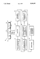
- FIG. 1 is an elevational view of an indium phosphide wafer substrate having a microelectronic device built thereon, with vias shown in phantom lines;
- FIG. 2 is a block diagram of a process for preparing the structure of FIG. 1.
- FIG. 1 depicts a microelectronic device 20 built upon a wafer 22 of indium phosphide (InP). (The elements are not shown to scale.)
- the microelectronic device 20 is indicated schematically as having two microelectronic components 24 deposited upon a front side 26 of the wafer 22.
- a metallic layer 28 is deposited upon a back side 30 of the wafer 22.
- Vias 32 are formed as small openings through the thickness of the wafer 22, and extend from the microelectronic components 24 on the front side 26 to the metallic layer 88 on the back side 30.
- signal reception and/or signal processing are performed by the microelectronic components 24.
- the metallic layer 28 and vias 32 may also provide electronic communication paths between the microelectronic components 24.
- the metallic layer 28 is usually patterned during or after deposition using conventional patterning techniques to produce connection pads and traces, but these features cannot be seen in the elevational view of FIG. 1.
- the precise nature of the microelectronic device 20 and patterning of the metallic layer 28 are not a part of the present invention, which is operable with any such structure.
- FIG. 2 depicts the procedure for preparing the microelectronic device 20 of FIG. 1.
- an indium phosphide piece is provided.
- the indium phosphide piece is preferably an oriented polycrystal with a cubic [001] direction of each grain perpendicular to the front side 26 and the back side 30. Such a piece may be cut from a larger directionally solidified Ingot of the indium phosphide material.
- the indium phosphide piece is typically a relatively thin disk having a diameter of about 2-3 inches and a thickness of about 0.025 inches.
- the indium phosphide piece is normally supplied much thicker than the final thickness of the wafer 22, to permit handling and deposition without fracture.
- the microelectronic components 24 are deposited on the front side 26 and the vias 32 are formed through the piece using known, conventional techniques appropriate for the particular components and vias being fabricated.
- the indium phosphide piece is next thinned to its final thickness from the back side 30 by lapping.
- lapping the indium phosphide piece is thinned by polishing the back side on a polishing wheel to slowly and uniformly remove material. (No material is removed from the front side, inasmuch as the microelectronic components are already in place on the front side.)
- the piece of indium phosphide is thinned to a thickness of about 0.004 inches by lapping.
- the details of this step 40 depend upon the exact nature of the microelectronic device 20, and are known in the art for each such device 20.
- the lapping operation to thin the indium phosphide piece to the desired final thickness of the wafer 22 leaves the back side 30 very smooth and polished.
- a later-deposited metallic layer will not adhere well to such a smooth, polished surface.
- the chemical treatment of the present invention roughens the surface of the back side 30 slightly without damaging the front side 26, the microelectronic components 24 on the front side, or the vias 32.
- a subsequently deposited metallic layer adheres well to this chemically toughened back side surface 30.
- the vias 32 are first masked, numeral 42, to prevent their damage (enlargement) by contact with the etching and chemical toughening solutions and to prevent the roughening solutions from penetrating through the vias to the microelectronic components 24 to damage them.
- the masking is preferably accomplished using any type of thick commercial photoresist, such as, For example, Shipley 4620.
- the indium phosphide piece is mounted with its front side 20 facing downwardly on a larger silicon piece. (The front side 26 and the microelectronic components 24 are thereby protected against subsequent attack in the etching and roughening solutions.)
- the silicon piece is placed on a spinner and the liquid photoresist is applied to the upwardly facing back side surface 30.
- the spinner is rotated at about 1000 revolutions per minute for about 30 seconds to spread the photoresist over the back side surface 30 and into the vias 32. Excess photoresist is spun away.
- the photoresist is next hardened according to the instructions for that particular type of photoresist.
- the wafer and photoresist are baked for 10 minutes at 75C-90 C, flood exposed with light or other radiation with the recommended dosage for the selected type of photoresist, and developed using the recommended developing procedure for the selected photoresist material.
- the developed wafer structure is rinsed in deionized water and dried with nitrogen.
- the finished photoresist-protected wafer is inspected carefully to verify full coverage and penetration into the vias. If any flaws in the photoresist coating of the vias are found, they are touched up with photoresist material. These steps are usually repeated two more times to ensure that all vias are filled with the thick photoresist material.
- the unmasked back side 90 of the wafer 22 is contacted with an etching solution, numeral 44.
- the etchant preferably is an aqueous solution of nitric acid and ceric ammonium nitrate (Ce(NH 4 ) 2 (NO 3 ) 6 ).
- the etching solution preferably has a composition of about 10-20 (most preferably, 12) percent by weight of nitric acid, about 10-20 (most preferably, 10) percent by weight of ceric ammonium nitrate, and the balance of water.
- Such an etchant is available commercially from KTI Chemicals as Chrome Etch.
- the back side 30 is contacted to the etching solution for about 5-15 minutes at ambient temperature. This etchant solution pits the back side surface 30 slightly, but does not produce the desired degree of surface roughening.
- the roughening solution is prepared and mixed, numeral 46.
- the preferred roughening solution has a composition of from about 4to about 6 parts by volume of acetic acid, and about 4 to about 6 parts by volume nitric acid, and about 1 part by volume hydrobromic acid.
- the selected composition achieves a balancing between strength and rate of attack. If the solution has less than about 4 parts of acetic acid and 4 parts of nitric acid, it too strong and attacks the indium phosphide and even the photoresist masking material at too high a rate. If the solution has more than about 6 parts of acetic acid and 6 parts nitric acid, its rate slows and becomes uneconomic and eventually ineffective.
- a most preferred roughening solution has about 4 parts by volume of acetic acid, about 4 parts by volume of nitric acid, and about 1 part by volume of hydrobromic acid.
- the solution is preferably stirred for 10 minutes under an exhaust hood to react the constituents together to produce bromine and nitrogen oxide.
- the roughening solution is contacted to the back side surface 30 of the wafer 22 , preferably by immersing the wafer into the solution at ambient temperature numeral 48. Exposure is for from about 15 to about 30 seconds, but in any case should not exceed 30 seconds because the photoresist and the underlying protected structure may be attacked by longer exposure.
- the wafer is removed from the roughening solution and cleaned to remove the reaction products, numeral 50.
- the surface is first washed in deionized water to remove the solution, and dried in nitrogen.
- the resulting exposed back side surface 30 of the wafer 22 is gray-black in color due to indium oxide residue from the reaction with the roughening solution.
- the residue can be removed by immersing the wafer in aqueous hydrofluoric acid solution, preferably 7 parts by volume water and 1part by volume hydrofluoric acid, for 10-15 seconds.
- the surface is again washed in deionized water and dried in nitrogen.
- the resulting back side 30 has a surface that is controllably roughened to a roughness of about 2-3 micrometers. When viewed at 100X magnification, the indium phosphide back side 30 has a pebbled, grainy appearance. When the procedure is performed as set forth herein, the vias 82, front side 26, and microelectronic components 24 are not attacked or damaged in any manner.
- the photoresist mask of the vias is removed, numeral 52.
- the photoresist can be removed by immersing the wafer in a suitable solvent for the photoresist material.
- a suitable solvent is acetone.
- the metallic layer 28 is deposited onto the back side 30 by any suitable process, such as electron beam evaporation or sputtering, numeral 54.
- the metal is typically titanium, platinum, or gold in a thickness of about 10,000 Angstroms.
- the metallic layer 28 can be deposited in a patterned form, or deposited as a uniform layer and subsequently patterned by conventional techniques.
- the present invention provides an approach for treating indium phosphide surfaces, Including surface toughening to improve the adherence of metallic coatings on the indium phosphide.
Abstract
Description
Claims (16)
Priority Applications (1)
| Application Number | Priority Date | Filing Date | Title |
|---|---|---|---|
| US08/134,129 US5334284A (en) | 1992-12-23 | 1993-10-12 | Surface treatment of indium phosphide utilizing chemical roughening of the surface |
Applications Claiming Priority (2)
| Application Number | Priority Date | Filing Date | Title |
|---|---|---|---|
| US99623292A | 1992-12-23 | 1992-12-23 | |
| US08/134,129 US5334284A (en) | 1992-12-23 | 1993-10-12 | Surface treatment of indium phosphide utilizing chemical roughening of the surface |
Related Parent Applications (1)
| Application Number | Title | Priority Date | Filing Date |
|---|---|---|---|
| US99623292A Continuation | 1992-12-23 | 1992-12-23 |
Publications (1)
| Publication Number | Publication Date |
|---|---|
| US5334284A true US5334284A (en) | 1994-08-02 |
Family
ID=25542656
Family Applications (1)
| Application Number | Title | Priority Date | Filing Date |
|---|---|---|---|
| US08/134,129 Expired - Lifetime US5334284A (en) | 1992-12-23 | 1993-10-12 | Surface treatment of indium phosphide utilizing chemical roughening of the surface |
Country Status (1)
| Country | Link |
|---|---|
| US (1) | US5334284A (en) |
Cited By (7)
| Publication number | Priority date | Publication date | Assignee | Title |
|---|---|---|---|---|
| EP0962764A2 (en) * | 1998-06-03 | 1999-12-08 | Delphi Technologies, Inc. | Electrical and chemical treatment of an oxygen sensor |
| US6107185A (en) * | 1999-04-29 | 2000-08-22 | Advanced Micro Devices, Inc. | Conductive material adhesion enhancement in damascene process for semiconductors |
| US6361821B1 (en) | 2000-12-13 | 2002-03-26 | Delphi Technologies, Inc. | Method of treating an exhaust sensor and a product thereof |
| US6638405B2 (en) * | 2001-09-10 | 2003-10-28 | Delphi Technologies, Inc. | Gas sensor and method of manufacturing the same |
| US6682640B2 (en) | 2002-06-13 | 2004-01-27 | Delphi Technologies, Inc. | Co-fired oxygen sensor elements |
| US20080247935A1 (en) * | 2004-03-19 | 2008-10-09 | Nippon Mining & Metals Co., Ltd. | Compound Semiconductor Substrate |
| US11094549B2 (en) * | 2017-07-25 | 2021-08-17 | Beijing Tongmei Xtal Technology Co., Ltd. | Indium phosphide wafer having pits on the back side, method and etching solution for manufacturing the same |
-
1993
- 1993-10-12 US US08/134,129 patent/US5334284A/en not_active Expired - Lifetime
Non-Patent Citations (6)
| Title |
|---|
| "Investigations of Etched Channels on Indium Phosphide And Gallium Arsenide Substrates"; 1985; abstract only; Latv. PSR Zinat. Akad. Vestis, Fiz Teh. Zinat Ser. (5). |
| "Local Etching of Indium Phosphide In Anisotropic Etchants"; 1985; abstract only; Izv. Akad. Nauk SSSR, Neorg, Mater., 21(8). |
| "Observation of Etch Pits Produced in InP By New Etchants", K. Akita, et al., pp. 783-787, Journal of Crystal Growth 46 (1979). |
| Investigations of Etched Channels on Indium Phosphide And Gallium Arsenide Substrates ; 1985; abstract only; Latv. PSR Zinat. Akad. Vestis, Fiz Teh. Zinat Ser. (5). * |
| Local Etching of Indium Phosphide In Anisotropic Etchants ; 1985; abstract only; Izv. Akad. Nauk SSSR, Neorg, Mater., 21(8). * |
| Observation of Etch Pits Produced in InP By New Etchants , K. Akita, et al., pp. 783 787, Journal of Crystal Growth 46 (1979). * |
Cited By (9)
| Publication number | Priority date | Publication date | Assignee | Title |
|---|---|---|---|---|
| EP0962764A2 (en) * | 1998-06-03 | 1999-12-08 | Delphi Technologies, Inc. | Electrical and chemical treatment of an oxygen sensor |
| US6179989B1 (en) * | 1998-06-03 | 2001-01-30 | General Motors Corporation | Electrical and chemical treatment of an oxygen sensor |
| EP0962764A3 (en) * | 1998-06-03 | 2001-12-19 | Delphi Technologies, Inc. | Electrical and chemical treatment of an oxygen sensor |
| US6107185A (en) * | 1999-04-29 | 2000-08-22 | Advanced Micro Devices, Inc. | Conductive material adhesion enhancement in damascene process for semiconductors |
| US6361821B1 (en) | 2000-12-13 | 2002-03-26 | Delphi Technologies, Inc. | Method of treating an exhaust sensor and a product thereof |
| US6638405B2 (en) * | 2001-09-10 | 2003-10-28 | Delphi Technologies, Inc. | Gas sensor and method of manufacturing the same |
| US6682640B2 (en) | 2002-06-13 | 2004-01-27 | Delphi Technologies, Inc. | Co-fired oxygen sensor elements |
| US20080247935A1 (en) * | 2004-03-19 | 2008-10-09 | Nippon Mining & Metals Co., Ltd. | Compound Semiconductor Substrate |
| US11094549B2 (en) * | 2017-07-25 | 2021-08-17 | Beijing Tongmei Xtal Technology Co., Ltd. | Indium phosphide wafer having pits on the back side, method and etching solution for manufacturing the same |
Similar Documents
| Publication | Publication Date | Title |
|---|---|---|
| US3962004A (en) | Pattern definition in an organic layer | |
| US5240878A (en) | Method for forming patterned films on a substrate | |
| US6245677B1 (en) | Backside chemical etching and polishing | |
| JP2004513515A (en) | Amorphous carbon layer for improved adhesion of photoresist | |
| JPS5812344B2 (en) | Method for forming metal patterns using copper as a base material | |
| US4106975A (en) | Process for etching holes | |
| JP3418307B2 (en) | Semiconductor device manufacturing method by pattern formation of wafer having non-planar surface | |
| US5334284A (en) | Surface treatment of indium phosphide utilizing chemical roughening of the surface | |
| US5126007A (en) | Method for etching a pattern in layer of gold | |
| EP0401314B1 (en) | Cryogenic process for metal lift-off | |
| JPS63294556A (en) | Improvement in adhesiveness of photoresist material for substrate | |
| JPS63170925A (en) | Formation of wiring on substrate and lift-off film | |
| US4704188A (en) | Wet chemical etching of crxsiynz | |
| JPS6251228A (en) | Manufacture of gallium-arsenide monolithic microwave integrated circuit | |
| JPS63127531A (en) | Manufacture of semiconductor device | |
| JPS6077148A (en) | Method for working glass substrate | |
| JPH08264490A (en) | Fabrication of semiconductor device | |
| JPH08144075A (en) | Removal of foreign matter on metal and device therefor | |
| JPS59117219A (en) | Manufacture of semiconductor device | |
| JPH07130685A (en) | Method of manufacturing semiconductor wafer | |
| JPS61121335A (en) | Processing method for grounding surface of wafer | |
| JPH0239432A (en) | Manufacture of semiconductor device | |
| JP3382218B2 (en) | Honing method for single crystal wafer | |
| JPH049292B2 (en) | ||
| JPS58202526A (en) | Manufacture of x-ray exposure mask |
Legal Events
| Date | Code | Title | Description |
|---|---|---|---|
| STCF | Information on status: patent grant |
Free format text: PATENTED CASE |
|
| AS | Assignment |
Owner name: AIR FORCE, UNITED STATES, VIRGINIA Free format text: CONFIRMATORY LICENSE;ASSIGNOR:HUGHES AIRCRAFT COMPANY;REEL/FRAME:007751/0215 Effective date: 19950425 |
|
| FPAY | Fee payment |
Year of fee payment: 4 |
|
| AS | Assignment |
Owner name: HUGHES ELECTRONICS CORPORATION, CALIFORNIA Free format text: ASSIGNMENT OF ASSIGNORS INTEREST;ASSIGNOR:HE HOLDINGS INC., HUGHES ELECTRONICS FORMERLY KNOWN AS HUGHES AIRCRAFT COMPANY;REEL/FRAME:009350/0366 Effective date: 19971217 |
|
| FEPP | Fee payment procedure |
Free format text: PAYOR NUMBER ASSIGNED (ORIGINAL EVENT CODE: ASPN); ENTITY STATUS OF PATENT OWNER: LARGE ENTITY Free format text: PAYER NUMBER DE-ASSIGNED (ORIGINAL EVENT CODE: RMPN); ENTITY STATUS OF PATENT OWNER: LARGE ENTITY |
|
| FPAY | Fee payment |
Year of fee payment: 8 |
|
| REMI | Maintenance fee reminder mailed | ||
| FPAY | Fee payment |
Year of fee payment: 12 |