US5202716A - Resist process system - Google Patents
Resist process system Download PDFInfo
- Publication number
- US5202716A US5202716A US07/904,505 US90450592A US5202716A US 5202716 A US5202716 A US 5202716A US 90450592 A US90450592 A US 90450592A US 5202716 A US5202716 A US 5202716A
- Authority
- US
- United States
- Prior art keywords
- wafer
- passage
- process system
- waiting
- resist process
- Prior art date
- Legal status (The legal status is an assumption and is not a legal conclusion. Google has not performed a legal analysis and makes no representation as to the accuracy of the status listed.)
- Expired - Lifetime
Links
Images


Classifications
-
- H10P72/0456—
-
- B—PERFORMING OPERATIONS; TRANSPORTING
- B29—WORKING OF PLASTICS; WORKING OF SUBSTANCES IN A PLASTIC STATE IN GENERAL
- B29C—SHAPING OR JOINING OF PLASTICS; SHAPING OF MATERIAL IN A PLASTIC STATE, NOT OTHERWISE PROVIDED FOR; AFTER-TREATMENT OF THE SHAPED PRODUCTS, e.g. REPAIRING
- B29C31/00—Handling, e.g. feeding of the material to be shaped, storage of plastics material before moulding; Automation, i.e. automated handling lines in plastics processing plants, e.g. using manipulators or robots
-
- G—PHYSICS
- G03—PHOTOGRAPHY; CINEMATOGRAPHY; ANALOGOUS TECHNIQUES USING WAVES OTHER THAN OPTICAL WAVES; ELECTROGRAPHY; HOLOGRAPHY
- G03F—PHOTOMECHANICAL PRODUCTION OF TEXTURED OR PATTERNED SURFACES, e.g. FOR PRINTING, FOR PROCESSING OF SEMICONDUCTOR DEVICES; MATERIALS THEREFOR; ORIGINALS THEREFOR; APPARATUS SPECIALLY ADAPTED THEREFOR
- G03F7/00—Photomechanical, e.g. photolithographic, production of textured or patterned surfaces, e.g. printing surfaces; Materials therefor, e.g. comprising photoresists; Apparatus specially adapted therefor
- G03F7/16—Coating processes; Apparatus therefor
-
- G—PHYSICS
- G03—PHOTOGRAPHY; CINEMATOGRAPHY; ANALOGOUS TECHNIQUES USING WAVES OTHER THAN OPTICAL WAVES; ELECTROGRAPHY; HOLOGRAPHY
- G03F—PHOTOMECHANICAL PRODUCTION OF TEXTURED OR PATTERNED SURFACES, e.g. FOR PRINTING, FOR PROCESSING OF SEMICONDUCTOR DEVICES; MATERIALS THEREFOR; ORIGINALS THEREFOR; APPARATUS SPECIALLY ADAPTED THEREFOR
- G03F7/00—Photomechanical, e.g. photolithographic, production of textured or patterned surfaces, e.g. printing surfaces; Materials therefor, e.g. comprising photoresists; Apparatus specially adapted therefor
- G03F7/26—Processing photosensitive materials; Apparatus therefor
- G03F7/30—Imagewise removal using liquid means
- G03F7/3021—Imagewise removal using liquid means from a wafer supported on a rotating chuck
-
- G—PHYSICS
- G03—PHOTOGRAPHY; CINEMATOGRAPHY; ANALOGOUS TECHNIQUES USING WAVES OTHER THAN OPTICAL WAVES; ELECTROGRAPHY; HOLOGRAPHY
- G03F—PHOTOMECHANICAL PRODUCTION OF TEXTURED OR PATTERNED SURFACES, e.g. FOR PRINTING, FOR PROCESSING OF SEMICONDUCTOR DEVICES; MATERIALS THEREFOR; ORIGINALS THEREFOR; APPARATUS SPECIALLY ADAPTED THEREFOR
- G03F7/00—Photomechanical, e.g. photolithographic, production of textured or patterned surfaces, e.g. printing surfaces; Materials therefor, e.g. comprising photoresists; Apparatus specially adapted therefor
- G03F7/70—Microphotolithographic exposure; Apparatus therefor
- G03F7/70691—Handling of masks or workpieces
- G03F7/70733—Handling masks and workpieces, e.g. exchange of workpiece or mask, transport of workpiece or mask
- G03F7/7075—Handling workpieces outside exposure position, e.g. SMIF box
-
- H10P72/0458—
-
- H10P72/3302—
Definitions
- the present invention relates to an apparatus for coating a photo-resist film on the surface of a substrate and/or, for developing the photo-resist film subsequent to being exposed with a predetermined pattern, which is used in the manufacture of a semiconductor device, such as an integrated circuit.
- the apparatus of the invention is effectively used in manufacturing various types of ASICs with small production in each type.
- a photoengraving process is of greater importance because of PEP provides the base of a present microfabrication technique.
- a predetermined resist pattern is formed on the surface of the wafer, the resist pattern being employed as, for example, an etching mask.
- the formation of the resist pattern by the PEP comprises the steps of coating a photo-resist on the wafer surface to provide a photo-resist film of uniform thickness, selectively exposing the photo-resist film at a predetermined area and developing the exposed photoresist film to form a desired pattern.
- an exposing device such as a step and repeat aligner (that is, a stepper).
- the step for forming the photo-resist film on the substrate surface is carried out with, for example, an apparatus as will be explained below in more detail.
- FIG. 1 is a flowchart showing the processing steps of a photo-resist film formation apparatus called a track system, including treating units carrying out a preheating step 4, cooling step 5, coating step 6 and heating step 8.
- Semiconductor wafers W are introduced into the aforementioned apparatus such that each is held within a cassette 2.
- the semiconductor wafers W are taken out of the cassette 2 sheet by sheet and conveyed by a belt conveying mechanism 3 sequentially to the respective units for performing the respective treatment to be carried out there.
- the wafer W has its moisture removed by heating and, subsequent to being cooled by the cooling step 5, is conveyed to the coating unit where a photo-resist is evenly coated on the surface of the wafer W by means of, for example, a spinner coater.
- the photo-resist-coated wafer W is sent to the heating unit 8 having a conveyor mechanism 7 called a walking beam system.
- the heating unit 8 the photo-resist solution on the wafer is converted into a stable film.
- the wafer W with a desired photo-resist thin film formed thereon is conveyed into cassette 10 where it is stored as a "treated" wafer.
- the respective independent treating units are installed in a serial array and a semiconductor wafer to be treated has to be conveyed inevitably past all these units in a "one-way" course in a predetermined order whether all these treatment is required or not. It is, therefore, not possible to freely change a "once-set" treating order or to cause the wafer to pass selectively through only a predetermined unit or units.
- the treating process necessary for forming an IC in the semiconductor wafer W differs depending upon the kinds of IC's to be formed on the wafer. In spite of some step or steps being unnecessary, it is unavoidable in the conventional apparatus that all the aforementioned steps have to be carried out on the semiconductor wafer. This cause a bar to the implementation of improved throughput.
- a resist process system comprises conveying means for conveying wafer; a passage along which the conveying means is movable; a plurality of process units arranged beside the passage; and at least one waiting unit for temporarily keeping the wafer which is to be processed; wherein said waiting unit is arranged beside the passage and between the process units.
- FIG. 1 is a block diagram showing the conventional resist processing system
- FIG. 2 is a plan showing a part of wafer loading/unloading and process sections
- FIG. 3 is a plan schematically showing the whole of the resist process system according to a first embodiment of the present invention
- FIG. 4 is a vertically-sectioned view showing a waiting section in the resist process system
- FIG. 5 is a plan schematically showing the whole of the resist process system according to a second embodiment of the present invention.
- FIG. 6 is a vertically-sectioned view showing a waiting section in the second resist process system
- FIG. 7 is a plan schematically showing the whole of the resist process system according to a third embodiment of the present invention.
- FIG. 8 is a plan schematically showing the whole of the resist process system according to a fourth embodiment of the present invention.
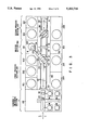
- FIG. 2 shows a plan view showing an apparatus 100 according to an embodiment of the present invention which is adapted to apply a photo-resist film on a semiconductor wafer surface and/or to develop the photoresist film subsequent to being exposed with a specific pattern.
- reference numeral 101 shows a body base of the apparatus.
- a passage 102 is provided at the middle of the body base 101 and extends in a lateral direction as indicated by an arrow Y in FIG. 2.
- On one side of the passage 102 are provided a prehearing unit 201a for eliminating moisture, etc.
- an adhesion unit 201b for applying HMDS the wafer a heating unit 202 for heating the wafer subsequent to, for example, being coated with the photoresist solution to dry it, and an exposing unit 203 for exposing the wafer.
- the heating unit 202 has upper heating plate and lower heating plate arranged in an overlapping fashion.
- a coating unit 204 and a developing unit 205 are provided on the other side of the passage 102.
- the applying unit 204 is provided in order to coat, a photo-resist solution on the surface of the wafer which has been preheated and cooled, or in order to spray a developing solution to an exposed photoresist film on the wafer.
- the preheating unit 201a and the adhesion unit 201b are shown provided in a plan array in FIG. 2 for convenience's sake, as a matter of fact, the preheating unit 201a is provided over the adhesion unit 201b.
- a wafer conveying device 110 is mounted on the passage 102 to allow the wafer to be travelled in the Y direction by a drive mechanism, not shown, such as a ball screw.
- a tweezer (handling arms 131, 132, 133) of the conveying device 110 can be moved to the X direction (the width direction of the passage 102), simultaneously in the Y direction (longitudinal direction of the passage 102) and the Z direction (vertical direction), and further can be rotated independently or simultaneously in the ⁇ direction as shown in FIG. 2.
- a stepping motor and drive mechanism not shown, such as a ball screw, are coupled to the carriage 116.
- the conveying device 110 is employed to convey the wafer W to a respective one of the aforementioned treatment units.
- a wafer loading/unloading mechanism 120 is provided to the left side of body base 101 and houses a plurality of wafer cassettes 122, 123 with those untreated semiconductor wafers W B held in the respective wafer cassettes 122 and those treated wafers W F held in the respective wafer cassettes 123.
- a pair of tweezers 121 is provided in the wafer loading/unloading mechanism 120 to hold the wafer W under a suction force imposed to the lower surface of the wafer. Like the tweezers 112 and 113, tweezers 121 can be moved in the X and Y directions and can pick up the untreated wafer W B from the cassette 122 and store the treated wafer W F into the wafer cassette 123.
- the pair of tweezers 121 of the wafer loading/unloading mechanism 120 delivers the untreated wafer W B to the tweezer of the conveying device 110 and receives the treated wafer W F from those tweezer of the conveying device 110. That deliver/receive interface is provided at a boundary between the passage 102 and the wafer loading/unloading mechanism 120.
- the delivering/receiving operation of the wafers is achieved relative to the respective treatment units by the tweezer of the conveying device 110.
- the wafer W undergoes various treatments at the respective units 201a to 205 in accordance with a predetermined order.
- the operation of conveying wafers is all controlled by a control system, not shown.
- the various treatments at the process units 201a to 205 can freely be set by modifying the program of a control system. That is, the treatments can be effected at some process units alone in accordance with a modified treatment sequence.
- a carriage passage 102 extends along the longitudinal center line of first and second process sections 200 and 250.
- Process units 206, 207 and 208 of the second process section 250 are arranged along the passage 102 on both sides thereof.
- a pair of rails 60 extends along the passage 102 at the sections 200 and 250.
- a first wafer conveying robot 110 runs on the rails 60 in the first section 200 and a second wafer conveying robot 210 runs also on the rails 60 in the second section 250.
- Stoppers 61 are arranged at both ends of the rails 60 which extend at the first process section 200 and also at both ends of the rails 60 which extend at the second process section 250. Each of these stoppers 61 includes a collision preventing sensor (not shown).
- a waiting section 300 including two units 301 is arranged between the first 200 and the second process section 250.
- the waiting units 301 are opposed to each other with the passage 102 interposed between them. They are positioned in a range where the first and second robots 110 and 210 which run on the rails 60 can gain access to them. They can be detached from their adjacent process units 203, 206 and 205, 208. They serve to transfer wafers between the first 200 and the second process section 250 and they also serve to temporarily keep the wafers.
- the rails 60 for the first robot 110 and those for the second robot 210 are separated in front of the waiting unit 301.
- arms 131, 132 and 133 of each of the robots 110 and 210 are extended oblique in relation to the rails 60, their front fork 134 can reach a stage 302 of each of the waiting units 301.
- each waiting section 301 includes four deck compartments vertically divided by partitions 306.
- the wafer stage 302 is arranged in the most upper deck compartment.
- the wafer stage 302 is shaped like a ring but cut away at its portion so as to allow the wafer to be mounted on and removed from it. It is fixed to the partition 306 by support rods 303.
- a cooling plate CP is arranged in the most lower compartment and heating plates HP are arranged in the second and third compartments, respectively.
- the wafer stage 302 may be arranged in the most lower or in any of the second and third compartments.
- Each of the units 201-208 and 301 is positioned on an air-conditioned body 100a and enclosed by a cover 100b.
- a body 116 of the robot 110 has two pairs of wheels 118 which run on the rails 60.
- a turntable 117 is arranged, rotatable on a horizontal plane, on the top portion of the body 116.
- a lifting shaft 119 is erected, extending upward, on the turntable 117.
- a base plate 131 is attached to the top of the lifting shaft 119 and the extensible arms 132 and 133 are arranged on the base plate 131.
- the extensible arms 132 and 133 are placed one upon the other and they can be slid relative to each other on the base plate 131.
- the wafer holder or fork 134 is attached to the front end of the upper arm 133. Photosensors (not shown) are attached to the wafer holder 134. This wafer holder 134 is described in detail in U.S. Pat. No. 4,958,722.
- Shaft rods of the wheels 118, turntable 117, lifting shaft 119 and extensible arms 132, 133 are connected to drive shafts of stepping motors (not shown), which are controlled by controllers backed up by a computer system.
- a silicon wafer W 8 inches in diameter, is carried from the loading/unloading section 120 to the first process section 200 by the first robot 110.
- the wafer W is adhesion-processed at the adhesion unit 201, resist-coated at the coating unit 204 and baked at the heating unit 202. After this baking process, it is carried into the cooling compartment of the waiting unit 301 and cooled there.
- the wafer W While the wafer W is being processed in this manner, another wafer W is exposed in the exposing unit 203 and a further wafer W is developed in the developing unit 205.
- These units at the first process section 200 are occupied by the wafers as described above, the first robot 110 runs directly to the waiting section 300 to place wafers W on the stages 302 in the unit 301.
- the second robot 210 takes out the wafers W from the waiting units 301 and carried them into the second process section 250 where a series of adhesion, resist-coating, exposing and developing processes are applied to them.
- wafers W can be more efficiently resist-processed using two waiting units 301 and two conveying robots 110, 210.
- each of the waiting units 301 is designed to save space in such a way that it can include plural compartments therein. This enables the whole of the process system to be made more compact in size. Therefore, atmosphere in the process system can be more easily made clean.
- the waiting units 301 are positioned not on that line which is on the rails 60 but on the same lines as the process units are positioned.
- the whole length of the process system can be therefore mode shorter and the system itself can be smaller-sized, accordingly. This is quite effective particularly to the resist process system in which wafers, 8 inches in diameter, are processed.
- the resist process system according to a second embodiment of the present invention will be described with reference to FIGS. 5 and 6. Description will be omitted on same components as those in the first resist process system.
- the waiting section 300 is arranged not on both sides of the rails 60 but on one side thereof, that is, between the exposing 203 and the developing unit 206.
- the rails 60 extend from one end to the other end of the process sections line and the first and second robots 110 and 210 run on the rails 60 in front of the waiting unit 301.
- the waiting unit 301 is opposed to the coating unit 208 in which a spin coater is housed.
- the waiting unit 301 is fundamentally same as that in the first embodiment.
- the first and second robots 110 and 210 can be positioned just in front of the waiting unit 301. Therefore, the stroke of each of the arms 132 and 133 of each robot can be made shorter.
- the resist process system according to a third embodiment of the present invention will be described with reference to FIG. 7. Same components as those in the first embodiment wall not be further described below.
- a waiting section 400 is arranged between the first 200 and the second process section 250.
- a waiting unit 401 is beside the rails 60 and positioned in front of the first and second robots 110 and 210 when these robots finish their running on the rails 60 toward it.
- Two wafer stages 402a and 402b are provided in the waiting unit 401.
- One wafer stage 402a is provided in front of the running area of the first robot 110 and the other wafer stage 402b is provided in front of the running area of the second robot 210.
- a handling device 403 is arranged between the wafer stages 402a and 402b. This handling device 403 is substantially same as the one 121 at the loading/unloading section 120.
- Each of the wafer stages 402a and 402b is substantially same as the one 302 in the first embodiment. However, the wafer stages 402a and 402b are not fixed to the frame but supported rotatable on a plane by the frame.
- a wafer W is taken out from the process unit 205 and carried to the waiting section 400 by the first robot 110.
- the first robot 110 is positioned in front of the first wafer stage 402a of the waiting unit 401 to mount the wafer W on the stage 402a.
- the first stage 402a is turned by a quarter to direct its cut-away portion toward the handling device 403.
- the wafer W is transferred from the first stage 402a to the second stage 402b by the handling device 403.
- the second robot 210 is then positioned in front of the waiting section 400 to carry the wafer W into the second process section 250.
- the first and second robots 110 and 210 can be positioned in front of the waiting unit 401. Therefore, the stroke of each of the arms 132 and 133 of each robot can be made shorter.
- the waiting unit 401 is positioned not on the extended line of the rails 60 but on the line of the process units.
- the whole length of the system can be thus made shorter and the system itself can be smaller-sized. This is quite effective particularly to the resist process system in which wafers, 8 inches in diameter, are processed.
- the resist process system according to a fourth embodiment of the present invention will be described referring to FIG. 8. A further description on same components as those in the first through third embodiments will be omitted.
- a waiting section 500 is arranged between the first 200 and the second process section 250.
- a waiting unit 501 is beside the rails 60 and it is positioned in front of the first and second robots 110 and 210 when they finish their running on the rails 60 toward it.
- Only one wafer stage 502 is provided in the waiting unit 501 and it is mounted on a travel device 503.
- Guide rails 504 are arranged at the waiting unit 501, extending parallel to the rails 60 in the passage 102. The single wafer stage 502 on the travel device 503 can be thus moved on the rails 504.
- the single wafer stage 502 is substantially same as the one 302 in the first embodiment.
- the travel device 503 is also substantially same as the body 116.
- a wafer W is taken out from the process unit 205 and carried into the waiting section 500 by the first robot 110.
- the first robot 110 is positioned in front of the wafer stage 502 in the waiting unit 501 to transfer the wafer a onto the stage 502.
- the wafer W is moved from the section 200 to the section 250.
- the second robot 210 is then positioned in front of the waiting section 500 to carry the wafer W from the waiting section 500 into the second process section 250.
- the rails 504 at the waiting unit 501 can be made shorter than those in the third embodiment.
- the length of the waiting unit 501 can be thus made shorter and the whole of the system can be made more small.
Landscapes
- Physics & Mathematics (AREA)
- General Physics & Mathematics (AREA)
- Engineering & Computer Science (AREA)
- Mechanical Engineering (AREA)
- Robotics (AREA)
- Exposure Of Semiconductors, Excluding Electron Or Ion Beam Exposure (AREA)
- Container, Conveyance, Adherence, Positioning, Of Wafer (AREA)
Abstract
Description
Claims (11)
Priority Applications (3)
| Application Number | Priority Date | Filing Date | Title |
|---|---|---|---|
| US07/904,505 US5202716A (en) | 1988-02-12 | 1992-06-25 | Resist process system |
| US08/031,464 US5339128A (en) | 1988-02-12 | 1993-03-15 | Resist processing method |
| US08/271,675 US5442416A (en) | 1988-02-12 | 1994-07-07 | Resist processing method |
Applications Claiming Priority (7)
| Application Number | Priority Date | Filing Date | Title |
|---|---|---|---|
| JP3021988 | 1988-02-12 | ||
| JP63-30219 | 1988-07-28 | ||
| US07/308,470 US4985722A (en) | 1988-02-12 | 1989-02-10 | Apparatus for coating a photo-resist film and/or developing it after being exposed |
| US07/627,357 US5177514A (en) | 1988-02-12 | 1990-12-14 | Apparatus for coating a photo-resist film and/or developing it after being exposed |
| JP31844191 | 1991-11-05 | ||
| JP3-318441 | 1991-11-05 | ||
| US07/904,505 US5202716A (en) | 1988-02-12 | 1992-06-25 | Resist process system |
Related Parent Applications (1)
| Application Number | Title | Priority Date | Filing Date |
|---|---|---|---|
| US07/627,357 Continuation-In-Part US5177514A (en) | 1988-02-12 | 1990-12-14 | Apparatus for coating a photo-resist film and/or developing it after being exposed |
Related Child Applications (1)
| Application Number | Title | Priority Date | Filing Date |
|---|---|---|---|
| US08/031,464 Continuation-In-Part US5339128A (en) | 1988-02-12 | 1993-03-15 | Resist processing method |
Publications (1)
| Publication Number | Publication Date |
|---|---|
| US5202716A true US5202716A (en) | 1993-04-13 |
Family
ID=27521203
Family Applications (1)
| Application Number | Title | Priority Date | Filing Date |
|---|---|---|---|
| US07/904,505 Expired - Lifetime US5202716A (en) | 1988-02-12 | 1992-06-25 | Resist process system |
Country Status (1)
| Country | Link |
|---|---|
| US (1) | US5202716A (en) |
Cited By (81)
| Publication number | Priority date | Publication date | Assignee | Title |
|---|---|---|---|---|
| US5339128A (en) * | 1988-02-12 | 1994-08-16 | Tokyo Electron Limited | Resist processing method |
| US5611655A (en) * | 1993-04-23 | 1997-03-18 | Tokyo Electron Limited | Vacuum process apparatus and vacuum processing method |
| US5651823A (en) * | 1993-07-16 | 1997-07-29 | Semiconductor Systems, Inc. | Clustered photolithography system |
| US5664254A (en) * | 1995-02-02 | 1997-09-02 | Tokyo Electron Limited | Substrate processing apparatus and substrate processing method |
| US5731678A (en) * | 1996-07-15 | 1998-03-24 | Semitool, Inc. | Processing head for semiconductor processing machines |
| US5766824A (en) * | 1993-07-16 | 1998-06-16 | Semiconductor Systems, Inc. | Method and apparatus for curing photoresist |
| US5779799A (en) * | 1996-06-21 | 1998-07-14 | Micron Technology, Inc. | Substrate coating apparatus |
| US5789890A (en) * | 1996-03-22 | 1998-08-04 | Genmark Automation | Robot having multiple degrees of freedom |
| US5820679A (en) * | 1993-07-15 | 1998-10-13 | Hitachi, Ltd. | Fabrication system and method having inter-apparatus transporter |
| US5899690A (en) * | 1996-09-05 | 1999-05-04 | Samsung Electronics Co., Ltd. | Thermal processing apparatus for semiconductor wafer |
| US5955857A (en) * | 1995-08-14 | 1999-09-21 | Hyundai Electronics Industries Co., Ltd. | Wafer conveyor system |
| US6121743A (en) * | 1996-03-22 | 2000-09-19 | Genmark Automation, Inc. | Dual robotic arm end effectors having independent yaw motion |
| US6126703A (en) * | 1996-11-19 | 2000-10-03 | Tokyo Electron Limited | Substrate processing apparatus having an interface section including two stacked substrate waiting table |
| US6168667B1 (en) * | 1997-05-30 | 2001-01-02 | Tokyo Electron Limited | Resist-processing apparatus |
| US6176667B1 (en) * | 1996-04-30 | 2001-01-23 | Applied Materials, Inc. | Multideck wafer processing system |
| WO2000068973A3 (en) * | 1999-05-07 | 2001-03-15 | Infineon Technologies Ag | System for treating wafers |
| US6268900B1 (en) * | 1998-09-28 | 2001-07-31 | Tokyo Electron Limited | Accommodating apparatus and substrate processing system |
| US20020034886A1 (en) * | 2000-09-15 | 2002-03-21 | Applied Materials, Inc. | Double dual slot load lock for process equipment |
| US6450750B1 (en) * | 1997-07-28 | 2002-09-17 | Applied Materials, Inc. | Multiple loadlock system |
| US6489741B1 (en) | 1998-08-25 | 2002-12-03 | Genmark Automation, Inc. | Robot motion compensation system |
| US6533531B1 (en) | 1998-12-29 | 2003-03-18 | Asml Us, Inc. | Device for handling wafers in microelectronic manufacturing |
| US20030127442A1 (en) * | 1994-12-07 | 2003-07-10 | Carglass Luxembourg Sarl-Zug Branch | Releasing of glazing panels |
| US6616394B1 (en) * | 1998-12-30 | 2003-09-09 | Silicon Valley Group | Apparatus for processing wafers |
| US6634845B1 (en) * | 1999-06-18 | 2003-10-21 | Tokyo Electron Limited | Transfer module and cluster system for semiconductor manufacturing process |
| US6697145B1 (en) * | 1994-09-12 | 2004-02-24 | Nikon Corporation | Substrate processing apparatus for coating photoresist on a substrate and forming a predetermined pattern on a substrate by exposure |
| US6702865B1 (en) * | 1998-04-04 | 2004-03-09 | Tokyo Electron Limited | Alignment processing mechanism and semiconductor processing device using it |
| US6758647B2 (en) * | 2001-12-18 | 2004-07-06 | Hitachi High-Technologies Corporation | System for producing wafers |
| US20050016454A1 (en) * | 1999-12-15 | 2005-01-27 | Applied Materials, Inc. | Dual substrate loadlock process equipment |
| US20050058440A1 (en) * | 2003-09-17 | 2005-03-17 | Dainippon Screen Mfg. Co., Ltd. | Thermal processing apparatus, thermal processing method, and substrate processing apparatus |
| US20050061240A1 (en) * | 2003-09-22 | 2005-03-24 | Dainippon Screen Mfg. Co., Ltd. | Substrate processing apparatus and substrate processing method |
| WO2004069698A3 (en) * | 2003-01-31 | 2005-03-24 | Aviza Tech Inc | Transport system having shared load-lock front-end assembly |
| US20050095088A1 (en) * | 2003-10-20 | 2005-05-05 | Applied Materials, Inc. | Load lock chamber for large area substrate processing system |
| US20050150757A1 (en) * | 1997-03-17 | 2005-07-14 | Applied Komatsu Technology, Inc. | Heated and cooled vacuum chamber shield |
| DE4412915B4 (en) * | 1993-05-03 | 2005-12-15 | Unaxis Balzers Ag | Plasma treatment plant, process for its operation and use thereof |
| FR2872502A1 (en) * | 2004-07-05 | 2006-01-06 | Ecole Norm Superieure Lyon | SURFACE MICROSTRUCTURING DEVICE |
| US20060098977A1 (en) * | 2004-11-10 | 2006-05-11 | Dainippon Screen Mfg. Co., Ltd. | Substrate processing apparatus and substrate processing method |
| US20060098979A1 (en) * | 2004-11-10 | 2006-05-11 | Dainippon Screen Mfg. Co., Ltd. | Substrate processing apparatus and substrate processing method |
| US20060127203A1 (en) * | 2004-12-09 | 2006-06-15 | Au Optronics Corp. | Cassette stocker and method of forming the same |
| US20060151735A1 (en) * | 2004-06-14 | 2006-07-13 | Jae-Chull Lee | Curved slit valve door with flexible coupling |
| US20060182615A1 (en) * | 2001-09-21 | 2006-08-17 | Shinichi Kurita | Method for transferring substrates in a load lock chamber |
| US20060273815A1 (en) * | 2005-06-06 | 2006-12-07 | Applied Materials, Inc. | Substrate support with integrated prober drive |
| US20060285945A1 (en) * | 2002-07-22 | 2006-12-21 | Christopher Hofmeister | Substrate processing apparatus |
| US20070006936A1 (en) * | 2005-07-07 | 2007-01-11 | Applied Materials, Inc. | Load lock chamber with substrate temperature regulation |
| CN1301545C (en) * | 2003-03-10 | 2007-02-21 | 精工爱普生株式会社 | Manufacturing apparatus of manufacturing object and manufacturing method of manufacturing object |
| US20070166031A1 (en) * | 2006-01-16 | 2007-07-19 | Tetsuya Hamada | Substrate processing apparatus |
| US20070166133A1 (en) * | 2006-01-13 | 2007-07-19 | Applied Materials, Inc. | Decoupled chamber body |
| US20070183871A1 (en) * | 2002-07-22 | 2007-08-09 | Christopher Hofmeister | Substrate processing apparatus |
| US20070181557A1 (en) * | 2006-02-09 | 2007-08-09 | Tokyo Electron Limited | Heat treatment apparatus, heat treatment method, and computer readable storage medium |
| US20070274810A1 (en) * | 2006-05-26 | 2007-11-29 | Holtkamp William H | Linearly distributed semiconductor workpiece processing tool |
| US20070280816A1 (en) * | 2006-06-02 | 2007-12-06 | Shinichi Kurita | Multiple slot load lock chamber and method of operation |
| US20080087214A1 (en) * | 2006-08-04 | 2008-04-17 | Jae-Chull Lee | Load lock chamber with decoupled slit valve door seal compartment |
| US20080170931A1 (en) * | 2007-01-15 | 2008-07-17 | Koji Hashimoto | Substrate processing apparatus and substrate processing method |
| US20080178460A1 (en) * | 2007-01-29 | 2008-07-31 | Woodruff Daniel J | Protected magnets and magnet shielding for processing microfeature workpieces, and associated systems and methods |
| US20080206020A1 (en) * | 2007-02-27 | 2008-08-28 | Smith John M | Flat-panel display processing tool with storage bays and multi-axis robot arms |
| US20080251019A1 (en) * | 2007-04-12 | 2008-10-16 | Sriram Krishnaswami | System and method for transferring a substrate into and out of a reduced volume chamber accommodating multiple substrates |
| US20080279672A1 (en) * | 2007-05-11 | 2008-11-13 | Bachrach Robert Z | Batch equipment robots and methods of stack to array work-piece transfer for photovoltaic factory |
| US20080279658A1 (en) * | 2007-05-11 | 2008-11-13 | Bachrach Robert Z | Batch equipment robots and methods within equipment work-piece transfer for photovoltaic factory |
| US20080292433A1 (en) * | 2007-05-11 | 2008-11-27 | Bachrach Robert Z | Batch equipment robots and methods of array to array work-piece transfer for photovoltaic factory |
| US20090000543A1 (en) * | 2007-06-29 | 2009-01-01 | Sokudo Co., Ltd. | Substrate treating apparatus |
| US20090139833A1 (en) * | 2007-11-30 | 2009-06-04 | Sokudo Co., Ltd. | Multi-line substrate treating apparatus |
| US20090142162A1 (en) * | 2007-11-30 | 2009-06-04 | Sokudo Co., Ltd. | Substrate treating apparatus with inter-unit buffers |
| US20090162179A1 (en) * | 2002-07-22 | 2009-06-25 | Brooks Automation, Inc. | Substrate processing apparatus |
| US20090169344A1 (en) * | 2003-02-27 | 2009-07-02 | Tokyo Electron Limited | Substrate processing apparatus and substrate processing method |
| US20090165712A1 (en) * | 2007-12-28 | 2009-07-02 | Sokudo Co., Ltd. | substrate treating apparatus with parallel substrate treatment lines |
| US20090165711A1 (en) * | 2007-12-28 | 2009-07-02 | Sokudo Co., Ltd. | Substrate treating apparatus with substrate reordering |
| US20100129526A1 (en) * | 2004-12-06 | 2010-05-27 | Sokudo Co., Ltd. | Substrate processing apparatus |
| US20100136257A1 (en) * | 2004-12-06 | 2010-06-03 | Sokudo Co., Ltd. | Substrate processing apparatus |
| US20100136492A1 (en) * | 2004-12-06 | 2010-06-03 | Sokudo Co., Ltd. | Substrate processing apparatus and substrate processing method |
| US20100192844A1 (en) * | 2009-01-30 | 2010-08-05 | Semes Co., Ltd. | Apparatus and method for treating substrate |
| US20100239986A1 (en) * | 2005-09-25 | 2010-09-23 | Sokudo Co., Ltd. | Substrate processing apparatus |
| US7845618B2 (en) | 2006-06-28 | 2010-12-07 | Applied Materials, Inc. | Valve door with ball coupling |
| US20110038692A1 (en) * | 2009-08-17 | 2011-02-17 | Brooks Automation, Inc. | Substrate processing apparatus |
| CN102630335A (en) * | 2010-05-07 | 2012-08-08 | 东京毅力科创株式会社 | Method for manufacturing semiconductor device and apparatus for manufacturing semiconductor device |
| US8371792B2 (en) | 2002-07-22 | 2013-02-12 | Brooks Automation, Inc. | Substrate processing apparatus |
| WO2013107766A1 (en) * | 2012-01-16 | 2013-07-25 | Tel Solar Ag | Vacuum deposition system |
| US9059224B2 (en) | 2009-01-30 | 2015-06-16 | Semes Co., Ltd. | System and method for treating substrate |
| US9184071B2 (en) | 2007-11-30 | 2015-11-10 | Screen Semiconductor Solutions Co., Ltd. | Multi-story substrate treating apparatus with flexible transport mechanisms and vertically divided treating units |
| CN105416964A (en) * | 2015-12-18 | 2016-03-23 | 苏州锐迪智能科技有限公司 | Novel high-capacity material storing system and storing and taking out method |
| US9666460B2 (en) * | 2013-11-20 | 2017-05-30 | Besi Switzerland Ag | Through type furnace for substrates comprising a longitudinal slit |
| DE19981278B4 (en) * | 1998-07-09 | 2020-01-09 | Murata Machinery, Ltd. | Device and method for providing a complete stack of wafers |
| US11282737B2 (en) * | 2018-02-15 | 2022-03-22 | Lam Research Corporation | Moving substrate transfer chamber |
Citations (3)
| Publication number | Priority date | Publication date | Assignee | Title |
|---|---|---|---|---|
| US4764076A (en) * | 1986-04-17 | 1988-08-16 | Varian Associates, Inc. | Valve incorporating wafer handling arm |
| US4917556A (en) * | 1986-04-28 | 1990-04-17 | Varian Associates, Inc. | Modular wafer transport and processing system |
| US5015177A (en) * | 1986-07-04 | 1991-05-14 | Canon Kabushiki Kaisha | Wafer handling apparatus |
-
1992
- 1992-06-25 US US07/904,505 patent/US5202716A/en not_active Expired - Lifetime
Patent Citations (3)
| Publication number | Priority date | Publication date | Assignee | Title |
|---|---|---|---|---|
| US4764076A (en) * | 1986-04-17 | 1988-08-16 | Varian Associates, Inc. | Valve incorporating wafer handling arm |
| US4917556A (en) * | 1986-04-28 | 1990-04-17 | Varian Associates, Inc. | Modular wafer transport and processing system |
| US5015177A (en) * | 1986-07-04 | 1991-05-14 | Canon Kabushiki Kaisha | Wafer handling apparatus |
Cited By (146)
| Publication number | Priority date | Publication date | Assignee | Title |
|---|---|---|---|---|
| US5442416A (en) * | 1988-02-12 | 1995-08-15 | Tokyo Electron Limited | Resist processing method |
| US5339128A (en) * | 1988-02-12 | 1994-08-16 | Tokyo Electron Limited | Resist processing method |
| US5611655A (en) * | 1993-04-23 | 1997-03-18 | Tokyo Electron Limited | Vacuum process apparatus and vacuum processing method |
| DE4412915B4 (en) * | 1993-05-03 | 2005-12-15 | Unaxis Balzers Ag | Plasma treatment plant, process for its operation and use thereof |
| US7310563B2 (en) | 1993-07-15 | 2007-12-18 | Renesas Technology Corp. | Fabrication system and fabrication method |
| US20100131093A1 (en) * | 1993-07-15 | 2010-05-27 | Renesas Technology Corp. | Fabrication system and fabrication method |
| US20060111802A1 (en) * | 1993-07-15 | 2006-05-25 | Renesas Technology Corp. | Fabrication system and fabrication method |
| US7062344B2 (en) | 1993-07-15 | 2006-06-13 | Renesas Technology Corp. | Fabrication system and fabrication method |
| US20040107020A1 (en) * | 1993-07-15 | 2004-06-03 | Hitachi, Ltd. | Fabrication system and fabrication method |
| US5820679A (en) * | 1993-07-15 | 1998-10-13 | Hitachi, Ltd. | Fabrication system and method having inter-apparatus transporter |
| US5858863A (en) * | 1993-07-15 | 1999-01-12 | Hitachi, Ltd. | Fabrication system and method having inter-apparatus transporter |
| US7603194B2 (en) | 1993-07-15 | 2009-10-13 | Renesas Technology Corp. | Fabrication system and fabrication method |
| US7392106B2 (en) | 1993-07-15 | 2008-06-24 | Renesas Technology Corp. | Fabrication system and fabrication method |
| US6099598A (en) * | 1993-07-15 | 2000-08-08 | Hitachi, Ltd. | Fabrication system and fabrication method |
| US5766824A (en) * | 1993-07-16 | 1998-06-16 | Semiconductor Systems, Inc. | Method and apparatus for curing photoresist |
| US5651823A (en) * | 1993-07-16 | 1997-07-29 | Semiconductor Systems, Inc. | Clustered photolithography system |
| US6697145B1 (en) * | 1994-09-12 | 2004-02-24 | Nikon Corporation | Substrate processing apparatus for coating photoresist on a substrate and forming a predetermined pattern on a substrate by exposure |
| US20030127442A1 (en) * | 1994-12-07 | 2003-07-10 | Carglass Luxembourg Sarl-Zug Branch | Releasing of glazing panels |
| US5664254A (en) * | 1995-02-02 | 1997-09-02 | Tokyo Electron Limited | Substrate processing apparatus and substrate processing method |
| USRE37470E1 (en) * | 1995-02-02 | 2001-12-18 | Tokyo Electron Limited | Substrate processing apparatus and substrate processing method |
| US5955857A (en) * | 1995-08-14 | 1999-09-21 | Hyundai Electronics Industries Co., Ltd. | Wafer conveyor system |
| US6037733A (en) * | 1996-03-22 | 2000-03-14 | Genmark Automation | Robot having multiple degrees of freedom |
| US6121743A (en) * | 1996-03-22 | 2000-09-19 | Genmark Automation, Inc. | Dual robotic arm end effectors having independent yaw motion |
| US5789890A (en) * | 1996-03-22 | 1998-08-04 | Genmark Automation | Robot having multiple degrees of freedom |
| US6176667B1 (en) * | 1996-04-30 | 2001-01-23 | Applied Materials, Inc. | Multideck wafer processing system |
| US6477440B1 (en) * | 1996-06-21 | 2002-11-05 | Micron Technology, Inc. | Methods of treating a semiconductor wafer |
| US6113694A (en) * | 1996-06-21 | 2000-09-05 | Micron Technology, Inc. | Substrate treatment apparatus |
| US6061605A (en) * | 1996-06-21 | 2000-05-09 | Micron Technology, Inc. | Methods of treating a semiconductor wafer |
| US5779799A (en) * | 1996-06-21 | 1998-07-14 | Micron Technology, Inc. | Substrate coating apparatus |
| US5731678A (en) * | 1996-07-15 | 1998-03-24 | Semitool, Inc. | Processing head for semiconductor processing machines |
| US5899690A (en) * | 1996-09-05 | 1999-05-04 | Samsung Electronics Co., Ltd. | Thermal processing apparatus for semiconductor wafer |
| US6264705B1 (en) * | 1996-11-19 | 2001-07-24 | Tokyo Electron Limited | Processing system |
| US6126703A (en) * | 1996-11-19 | 2000-10-03 | Tokyo Electron Limited | Substrate processing apparatus having an interface section including two stacked substrate waiting table |
| US20050150757A1 (en) * | 1997-03-17 | 2005-07-14 | Applied Komatsu Technology, Inc. | Heated and cooled vacuum chamber shield |
| US6168667B1 (en) * | 1997-05-30 | 2001-01-02 | Tokyo Electron Limited | Resist-processing apparatus |
| SG92697A1 (en) * | 1997-05-30 | 2002-11-19 | Tokyo Electron Ltd | Resist-processing apparatus |
| US6450750B1 (en) * | 1997-07-28 | 2002-09-17 | Applied Materials, Inc. | Multiple loadlock system |
| US6702865B1 (en) * | 1998-04-04 | 2004-03-09 | Tokyo Electron Limited | Alignment processing mechanism and semiconductor processing device using it |
| EP1079429A4 (en) * | 1998-04-04 | 2005-06-29 | Tokyo Electron Ltd | ALIGNMENT MECHANISM AND SEMICONDUCTOR PROCESSING DEVICE USING THE MECHANISM |
| DE19981278B4 (en) * | 1998-07-09 | 2020-01-09 | Murata Machinery, Ltd. | Device and method for providing a complete stack of wafers |
| US6489741B1 (en) | 1998-08-25 | 2002-12-03 | Genmark Automation, Inc. | Robot motion compensation system |
| US6268900B1 (en) * | 1998-09-28 | 2001-07-31 | Tokyo Electron Limited | Accommodating apparatus and substrate processing system |
| US6533531B1 (en) | 1998-12-29 | 2003-03-18 | Asml Us, Inc. | Device for handling wafers in microelectronic manufacturing |
| US6616394B1 (en) * | 1998-12-30 | 2003-09-09 | Silicon Valley Group | Apparatus for processing wafers |
| US6809510B2 (en) | 1999-05-07 | 2004-10-26 | Infineon Technologies Ag | Configuration in which wafers are individually supplied to fabrication units and measuring units located in a fabrication cell |
| WO2000068973A3 (en) * | 1999-05-07 | 2001-03-15 | Infineon Technologies Ag | System for treating wafers |
| US6634845B1 (en) * | 1999-06-18 | 2003-10-21 | Tokyo Electron Limited | Transfer module and cluster system for semiconductor manufacturing process |
| US7641434B2 (en) | 1999-12-15 | 2010-01-05 | Applied Materials, Inc. | Dual substrate loadlock process equipment |
| US20050016454A1 (en) * | 1999-12-15 | 2005-01-27 | Applied Materials, Inc. | Dual substrate loadlock process equipment |
| US6949143B1 (en) | 1999-12-15 | 2005-09-27 | Applied Materials, Inc. | Dual substrate loadlock process equipment |
| US20020034886A1 (en) * | 2000-09-15 | 2002-03-21 | Applied Materials, Inc. | Double dual slot load lock for process equipment |
| US7105463B2 (en) | 2000-09-15 | 2006-09-12 | Applied Materials, Inc. | Load lock chamber having two dual slot regions |
| US7316966B2 (en) | 2001-09-21 | 2008-01-08 | Applied Materials, Inc. | Method for transferring substrates in a load lock chamber |
| US8616820B2 (en) | 2001-09-21 | 2013-12-31 | Applied Materials, Inc. | Double dual slot load lock chamber |
| US20080044259A1 (en) * | 2001-09-21 | 2008-02-21 | Shinichi Kurita | Double dual slot load lock chamber |
| US20060182615A1 (en) * | 2001-09-21 | 2006-08-17 | Shinichi Kurita | Method for transferring substrates in a load lock chamber |
| US6758647B2 (en) * | 2001-12-18 | 2004-07-06 | Hitachi High-Technologies Corporation | System for producing wafers |
| US20040146379A1 (en) * | 2001-12-18 | 2004-07-29 | Tetsunori Kaji | System and method of producing wafer |
| US8371792B2 (en) | 2002-07-22 | 2013-02-12 | Brooks Automation, Inc. | Substrate processing apparatus |
| US20070183871A1 (en) * | 2002-07-22 | 2007-08-09 | Christopher Hofmeister | Substrate processing apparatus |
| US20060285945A1 (en) * | 2002-07-22 | 2006-12-21 | Christopher Hofmeister | Substrate processing apparatus |
| US8827617B2 (en) | 2002-07-22 | 2014-09-09 | Brooks Automation Inc. | Substrate processing apparatus |
| US20090162179A1 (en) * | 2002-07-22 | 2009-06-25 | Brooks Automation, Inc. | Substrate processing apparatus |
| US8960099B2 (en) | 2002-07-22 | 2015-02-24 | Brooks Automation, Inc | Substrate processing apparatus |
| US9570330B2 (en) | 2002-07-22 | 2017-02-14 | Brooks Automation, Inc. | Substrate processing apparatus |
| US7959395B2 (en) | 2002-07-22 | 2011-06-14 | Brooks Automation, Inc. | Substrate processing apparatus |
| US8651789B2 (en) | 2002-07-22 | 2014-02-18 | Brooks Automation, Inc. | Substrate processing apparatus |
| US20110232844A1 (en) * | 2002-07-22 | 2011-09-29 | Brooks Automation, Inc. | Substrate processing apparatus |
| WO2004069698A3 (en) * | 2003-01-31 | 2005-03-24 | Aviza Tech Inc | Transport system having shared load-lock front-end assembly |
| US20090169344A1 (en) * | 2003-02-27 | 2009-07-02 | Tokyo Electron Limited | Substrate processing apparatus and substrate processing method |
| CN1301545C (en) * | 2003-03-10 | 2007-02-21 | 精工爱普生株式会社 | Manufacturing apparatus of manufacturing object and manufacturing method of manufacturing object |
| US7522823B2 (en) * | 2003-09-17 | 2009-04-21 | Sokudo Co., Ltd. | Thermal processing apparatus, thermal processing method, and substrate processing apparatus |
| US20050058440A1 (en) * | 2003-09-17 | 2005-03-17 | Dainippon Screen Mfg. Co., Ltd. | Thermal processing apparatus, thermal processing method, and substrate processing apparatus |
| US7229240B2 (en) * | 2003-09-22 | 2007-06-12 | Dainippon Screen Mfg. Co., Ltd. | Substrate processing apparatus and substrate processing method |
| US20050061240A1 (en) * | 2003-09-22 | 2005-03-24 | Dainippon Screen Mfg. Co., Ltd. | Substrate processing apparatus and substrate processing method |
| US20050095088A1 (en) * | 2003-10-20 | 2005-05-05 | Applied Materials, Inc. | Load lock chamber for large area substrate processing system |
| US7207766B2 (en) | 2003-10-20 | 2007-04-24 | Applied Materials, Inc. | Load lock chamber for large area substrate processing system |
| US7651315B2 (en) | 2003-10-20 | 2010-01-26 | Applied Materials, Inc. | Large area substrate transferring method for aligning with horizontal actuation of lever arm |
| US20070140814A1 (en) * | 2003-10-20 | 2007-06-21 | Shinichi Kurita | Large area substrate transferring method |
| US20060151735A1 (en) * | 2004-06-14 | 2006-07-13 | Jae-Chull Lee | Curved slit valve door with flexible coupling |
| US7497414B2 (en) | 2004-06-14 | 2009-03-03 | Applied Materials, Inc. | Curved slit valve door with flexible coupling |
| JP2008506145A (en) * | 2004-07-05 | 2008-02-28 | エコール ノルマル スプリュール ドゥ リヨン | Surface microstructuring device |
| US20080149272A1 (en) * | 2004-07-05 | 2008-06-26 | Ecole Normale Superieure De Lyon | Surface Microstructuring Device |
| FR2872502A1 (en) * | 2004-07-05 | 2006-01-06 | Ecole Norm Superieure Lyon | SURFACE MICROSTRUCTURING DEVICE |
| WO2006013257A1 (en) * | 2004-07-05 | 2006-02-09 | Ecole Normale Superieure De Lyon | Surface microstructuring device |
| US7658560B2 (en) | 2004-11-10 | 2010-02-09 | Dainippon Screen Mfg. Co., Ltd. | Substrate processing apparatus |
| US20100190116A1 (en) * | 2004-11-10 | 2010-07-29 | Sokudo Co., Ltd. | Substrate processing apparatus and substrate processing method |
| US20060098977A1 (en) * | 2004-11-10 | 2006-05-11 | Dainippon Screen Mfg. Co., Ltd. | Substrate processing apparatus and substrate processing method |
| US20060098979A1 (en) * | 2004-11-10 | 2006-05-11 | Dainippon Screen Mfg. Co., Ltd. | Substrate processing apparatus and substrate processing method |
| US8496761B2 (en) | 2004-11-10 | 2013-07-30 | Sokudo Co., Ltd. | Substrate processing apparatus and substrate processing method |
| US20100136492A1 (en) * | 2004-12-06 | 2010-06-03 | Sokudo Co., Ltd. | Substrate processing apparatus and substrate processing method |
| US8585830B2 (en) | 2004-12-06 | 2013-11-19 | Sokudo Co., Ltd. | Substrate processing apparatus and substrate processing method |
| US20100129526A1 (en) * | 2004-12-06 | 2010-05-27 | Sokudo Co., Ltd. | Substrate processing apparatus |
| US9703199B2 (en) | 2004-12-06 | 2017-07-11 | Screen Semiconductor Solutions Co., Ltd. | Substrate processing apparatus |
| US20100136257A1 (en) * | 2004-12-06 | 2010-06-03 | Sokudo Co., Ltd. | Substrate processing apparatus |
| US20060127203A1 (en) * | 2004-12-09 | 2006-06-15 | Au Optronics Corp. | Cassette stocker and method of forming the same |
| US20060273815A1 (en) * | 2005-06-06 | 2006-12-07 | Applied Materials, Inc. | Substrate support with integrated prober drive |
| US20070006936A1 (en) * | 2005-07-07 | 2007-01-11 | Applied Materials, Inc. | Load lock chamber with substrate temperature regulation |
| US8540824B2 (en) | 2005-09-25 | 2013-09-24 | Sokudo Co., Ltd. | Substrate processing method |
| US20100239986A1 (en) * | 2005-09-25 | 2010-09-23 | Sokudo Co., Ltd. | Substrate processing apparatus |
| US7845891B2 (en) | 2006-01-13 | 2010-12-07 | Applied Materials, Inc. | Decoupled chamber body |
| US20070166133A1 (en) * | 2006-01-13 | 2007-07-19 | Applied Materials, Inc. | Decoupled chamber body |
| US7722267B2 (en) * | 2006-01-16 | 2010-05-25 | Sokudo Co., Ltd. | Substrate processing apparatus |
| US20070166031A1 (en) * | 2006-01-16 | 2007-07-19 | Tetsuya Hamada | Substrate processing apparatus |
| US20070181557A1 (en) * | 2006-02-09 | 2007-08-09 | Tokyo Electron Limited | Heat treatment apparatus, heat treatment method, and computer readable storage medium |
| US7628612B2 (en) * | 2006-02-09 | 2009-12-08 | Tokyo Electron Limited | Heat treatment apparatus, heat treatment method, and computer readable storage medium |
| US20070274810A1 (en) * | 2006-05-26 | 2007-11-29 | Holtkamp William H | Linearly distributed semiconductor workpiece processing tool |
| US8398355B2 (en) | 2006-05-26 | 2013-03-19 | Brooks Automation, Inc. | Linearly distributed semiconductor workpiece processing tool |
| US7665951B2 (en) | 2006-06-02 | 2010-02-23 | Applied Materials, Inc. | Multiple slot load lock chamber and method of operation |
| US20070280816A1 (en) * | 2006-06-02 | 2007-12-06 | Shinichi Kurita | Multiple slot load lock chamber and method of operation |
| US7845618B2 (en) | 2006-06-28 | 2010-12-07 | Applied Materials, Inc. | Valve door with ball coupling |
| US8124907B2 (en) | 2006-08-04 | 2012-02-28 | Applied Materials, Inc. | Load lock chamber with decoupled slit valve door seal compartment |
| US20080087214A1 (en) * | 2006-08-04 | 2008-04-17 | Jae-Chull Lee | Load lock chamber with decoupled slit valve door seal compartment |
| US20080170931A1 (en) * | 2007-01-15 | 2008-07-17 | Koji Hashimoto | Substrate processing apparatus and substrate processing method |
| US20080178460A1 (en) * | 2007-01-29 | 2008-07-31 | Woodruff Daniel J | Protected magnets and magnet shielding for processing microfeature workpieces, and associated systems and methods |
| US20080206020A1 (en) * | 2007-02-27 | 2008-08-28 | Smith John M | Flat-panel display processing tool with storage bays and multi-axis robot arms |
| US20080251019A1 (en) * | 2007-04-12 | 2008-10-16 | Sriram Krishnaswami | System and method for transferring a substrate into and out of a reduced volume chamber accommodating multiple substrates |
| US20080279672A1 (en) * | 2007-05-11 | 2008-11-13 | Bachrach Robert Z | Batch equipment robots and methods of stack to array work-piece transfer for photovoltaic factory |
| US20080292433A1 (en) * | 2007-05-11 | 2008-11-27 | Bachrach Robert Z | Batch equipment robots and methods of array to array work-piece transfer for photovoltaic factory |
| US20080279658A1 (en) * | 2007-05-11 | 2008-11-13 | Bachrach Robert Z | Batch equipment robots and methods within equipment work-piece transfer for photovoltaic factory |
| US9230834B2 (en) | 2007-06-29 | 2016-01-05 | Screen Semiconductor Solutions Co., Ltd. | Substrate treating apparatus |
| US10290521B2 (en) | 2007-06-29 | 2019-05-14 | Screen Semiconductor Solutions Co., Ltd. | Substrate treating apparatus with parallel gas supply pipes and a gas exhaust pipe |
| US20090000543A1 (en) * | 2007-06-29 | 2009-01-01 | Sokudo Co., Ltd. | Substrate treating apparatus |
| US9174235B2 (en) | 2007-06-29 | 2015-11-03 | Screen Semiconductor Solutions Co., Ltd. | Substrate treating apparatus using horizontal treatment cell arrangements with parallel treatment lines |
| US9165807B2 (en) | 2007-06-29 | 2015-10-20 | Screen Semiconductor Solutions Co., Ltd. | Substrate treating apparatus with vertical treatment arrangement including vertical blowout and exhaust units |
| US8545118B2 (en) | 2007-11-30 | 2013-10-01 | Sokudo Co., Ltd. | Substrate treating apparatus with inter-unit buffers |
| US20090139833A1 (en) * | 2007-11-30 | 2009-06-04 | Sokudo Co., Ltd. | Multi-line substrate treating apparatus |
| US9687874B2 (en) | 2007-11-30 | 2017-06-27 | Screen Semiconductor Solutions Co., Ltd. | Multi-story substrate treating apparatus with flexible transport mechanisms and vertically divided treating units |
| US8708587B2 (en) | 2007-11-30 | 2014-04-29 | Sokudo Co., Ltd. | Substrate treating apparatus with inter-unit buffers |
| US20090142162A1 (en) * | 2007-11-30 | 2009-06-04 | Sokudo Co., Ltd. | Substrate treating apparatus with inter-unit buffers |
| US9184071B2 (en) | 2007-11-30 | 2015-11-10 | Screen Semiconductor Solutions Co., Ltd. | Multi-story substrate treating apparatus with flexible transport mechanisms and vertically divided treating units |
| US9368383B2 (en) | 2007-12-28 | 2016-06-14 | Screen Semiconductor Solutions Co., Ltd. | Substrate treating apparatus with substrate reordering |
| US20090165712A1 (en) * | 2007-12-28 | 2009-07-02 | Sokudo Co., Ltd. | substrate treating apparatus with parallel substrate treatment lines |
| US12217986B2 (en) | 2007-12-28 | 2025-02-04 | Screen Semiconductor Solutions Co., Ltd. | Substrate treating apparatus with parallel first and second parts of substrate treatment lines on multiple stories for simultaneously treating a plurality of substrates |
| US9299596B2 (en) | 2007-12-28 | 2016-03-29 | Screen Semiconductor Solutions Co., Ltd. | Substrate treating apparatus with parallel substrate treatment lines simultaneously treating a plurality of substrates |
| US20090165711A1 (en) * | 2007-12-28 | 2009-07-02 | Sokudo Co., Ltd. | Substrate treating apparatus with substrate reordering |
| US9059224B2 (en) | 2009-01-30 | 2015-06-16 | Semes Co., Ltd. | System and method for treating substrate |
| US20100192844A1 (en) * | 2009-01-30 | 2010-08-05 | Semes Co., Ltd. | Apparatus and method for treating substrate |
| US20110038692A1 (en) * | 2009-08-17 | 2011-02-17 | Brooks Automation, Inc. | Substrate processing apparatus |
| US8602706B2 (en) | 2009-08-17 | 2013-12-10 | Brooks Automation, Inc. | Substrate processing apparatus |
| CN102630335A (en) * | 2010-05-07 | 2012-08-08 | 东京毅力科创株式会社 | Method for manufacturing semiconductor device and apparatus for manufacturing semiconductor device |
| WO2013107766A1 (en) * | 2012-01-16 | 2013-07-25 | Tel Solar Ag | Vacuum deposition system |
| US9666460B2 (en) * | 2013-11-20 | 2017-05-30 | Besi Switzerland Ag | Through type furnace for substrates comprising a longitudinal slit |
| CN105416964B (en) * | 2015-12-18 | 2018-06-26 | 苏州锐迪智能科技有限公司 | A kind of novel high-capacity material storage system and access method |
| CN105416964A (en) * | 2015-12-18 | 2016-03-23 | 苏州锐迪智能科技有限公司 | Novel high-capacity material storing system and storing and taking out method |
| US11282737B2 (en) * | 2018-02-15 | 2022-03-22 | Lam Research Corporation | Moving substrate transfer chamber |
Similar Documents
| Publication | Publication Date | Title |
|---|---|---|
| US5202716A (en) | Resist process system | |
| US5339128A (en) | Resist processing method | |
| US5177514A (en) | Apparatus for coating a photo-resist film and/or developing it after being exposed | |
| JP3779393B2 (en) | Processing system | |
| US5297910A (en) | Transportation-transfer device for an object of treatment | |
| JP3579228B2 (en) | Substrate processing equipment | |
| JP2919925B2 (en) | Processing equipment | |
| JPH1092733A (en) | Processing system | |
| US6264705B1 (en) | Processing system | |
| US6309116B1 (en) | Substrate processing system | |
| JP2000353648A (en) | Substrate processing equipment | |
| JPH02132840A (en) | Manufacturing device | |
| JP2859849B2 (en) | Processing device and processing method | |
| JP2926703B2 (en) | Substrate processing method and apparatus | |
| JP2926213B2 (en) | Substrate processing equipment | |
| JPH11251405A (en) | Substrate processing equipment | |
| JP2926593B2 (en) | Substrate processing apparatus, resist processing apparatus, substrate processing method, and resist processing method | |
| JPH07176590A (en) | Processor | |
| JP2926592B2 (en) | Substrate processing equipment | |
| JP2926214B2 (en) | Apparatus and method for manufacturing substrate to be processed | |
| JP3246659B2 (en) | Resist processing apparatus, liquid processing apparatus, and substrate processing apparatus | |
| JP2877744B2 (en) | Semiconductor substrate resist processing equipment | |
| JP3441365B2 (en) | Substrate transfer device and substrate processing device | |
| JP2002208554A (en) | Substrate processing equipment | |
| JPH07176589A (en) | Manufacturing apparatus and manufacturing method |
Legal Events
| Date | Code | Title | Description |
|---|---|---|---|
| AS | Assignment |
Owner name: TOKYO ELECTRON KYUSHU LIMITED A CORP. OF JAPAN, Free format text: ASSIGNMENT OF ASSIGNORS INTEREST.;ASSIGNORS:TATEYAMA, KIYOHISA;AKIMOTO, MASAMI;USHIJIMA, MITSURU;REEL/FRAME:006241/0404;SIGNING DATES FROM 19920619 TO 19920625 Owner name: TOKYO ELECTRON LIMITED, JAPAN Free format text: ASSIGNMENT OF ASSIGNORS INTEREST.;ASSIGNORS:TATEYAMA, KIYOHISA;AKIMOTO, MASAMI;USHIJIMA, MITSURU;REEL/FRAME:006241/0404;SIGNING DATES FROM 19920619 TO 19920625 |
|
| STCF | Information on status: patent grant |
Free format text: PATENTED CASE |
|
| FEPP | Fee payment procedure |
Free format text: PAYOR NUMBER ASSIGNED (ORIGINAL EVENT CODE: ASPN); ENTITY STATUS OF PATENT OWNER: LARGE ENTITY |
|
| FPAY | Fee payment |
Year of fee payment: 4 |
|
| AS | Assignment |
Owner name: TOKYO ELECTRON LIMITED, JAPAN Free format text: ASSIGNMENT OF ASSIGNORS INTEREST;ASSIGNOR:TOKYO ELECTRON KYUSHU LIMITED;REEL/FRAME:009453/0220 Effective date: 19980513 |
|
| FPAY | Fee payment |
Year of fee payment: 8 |
|
| FEPP | Fee payment procedure |
Free format text: PAYOR NUMBER ASSIGNED (ORIGINAL EVENT CODE: ASPN); ENTITY STATUS OF PATENT OWNER: LARGE ENTITY Free format text: PAYER NUMBER DE-ASSIGNED (ORIGINAL EVENT CODE: RMPN); ENTITY STATUS OF PATENT OWNER: LARGE ENTITY |
|
| FPAY | Fee payment |
Year of fee payment: 12 |