US5189261A - Electrical and/or thermal interconnections and methods for obtaining such - Google Patents
Electrical and/or thermal interconnections and methods for obtaining such Download PDFInfo
- Publication number
- US5189261A US5189261A US07/598,466 US59846690A US5189261A US 5189261 A US5189261 A US 5189261A US 59846690 A US59846690 A US 59846690A US 5189261 A US5189261 A US 5189261A
- Authority
- US
- United States
- Prior art keywords
- metallic
- solder
- dielectric substrate
- card
- stud
- Prior art date
- Legal status (The legal status is an assumption and is not a legal conclusion. Google has not performed a legal analysis and makes no representation as to the accuracy of the status listed.)
- Expired - Fee Related
Links
Images


Classifications
-
- H—ELECTRICITY
- H10—SEMICONDUCTOR DEVICES; ELECTRIC SOLID-STATE DEVICES NOT OTHERWISE PROVIDED FOR
- H10W—GENERIC PACKAGES, INTERCONNECTIONS, CONNECTORS OR OTHER CONSTRUCTIONAL DETAILS OF DEVICES COVERED BY CLASS H10
- H10W70/00—Package substrates; Interposers; Redistribution layers [RDL]
- H10W70/60—Insulating or insulated package substrates; Interposers; Redistribution layers
- H10W70/611—Insulating or insulated package substrates; Interposers; Redistribution layers for connecting multiple chips together
-
- H—ELECTRICITY
- H05—ELECTRIC TECHNIQUES NOT OTHERWISE PROVIDED FOR
- H05K—PRINTED CIRCUITS; CASINGS OR CONSTRUCTIONAL DETAILS OF ELECTRIC APPARATUS; MANUFACTURE OF ASSEMBLAGES OF ELECTRICAL COMPONENTS
- H05K3/00—Apparatus or processes for manufacturing printed circuits
- H05K3/40—Forming printed elements for providing electric connections to or between printed circuits
- H05K3/4038—Through-connections; Vertical interconnect access [VIA] connections
- H05K3/4046—Through-connections; Vertical interconnect access [VIA] connections using auxiliary conductive elements, e.g. metallic spheres, eyelets, pieces of wire
-
- H—ELECTRICITY
- H05—ELECTRIC TECHNIQUES NOT OTHERWISE PROVIDED FOR
- H05K—PRINTED CIRCUITS; CASINGS OR CONSTRUCTIONAL DETAILS OF ELECTRIC APPARATUS; MANUFACTURE OF ASSEMBLAGES OF ELECTRICAL COMPONENTS
- H05K3/00—Apparatus or processes for manufacturing printed circuits
- H05K3/44—Manufacturing insulated metal core circuits or other insulated electrically conductive core circuits
-
- H—ELECTRICITY
- H10—SEMICONDUCTOR DEVICES; ELECTRIC SOLID-STATE DEVICES NOT OTHERWISE PROVIDED FOR
- H10W—GENERIC PACKAGES, INTERCONNECTIONS, CONNECTORS OR OTHER CONSTRUCTIONAL DETAILS OF DEVICES COVERED BY CLASS H10
- H10W70/00—Package substrates; Interposers; Redistribution layers [RDL]
- H10W70/60—Insulating or insulated package substrates; Interposers; Redistribution layers
- H10W70/62—Insulating or insulated package substrates; Interposers; Redistribution layers characterised by their interconnections
- H10W70/63—Vias, e.g. via plugs
- H10W70/635—Through-vias
-
- H—ELECTRICITY
- H05—ELECTRIC TECHNIQUES NOT OTHERWISE PROVIDED FOR
- H05K—PRINTED CIRCUITS; CASINGS OR CONSTRUCTIONAL DETAILS OF ELECTRIC APPARATUS; MANUFACTURE OF ASSEMBLAGES OF ELECTRICAL COMPONENTS
- H05K1/00—Printed circuits
- H05K1/02—Details
- H05K1/0201—Thermal arrangements, e.g. for cooling, heating or preventing overheating
- H05K1/0203—Cooling of mounted components
- H05K1/0204—Cooling of mounted components using means for thermal conduction connection in the thickness direction of the substrate
- H05K1/0206—Cooling of mounted components using means for thermal conduction connection in the thickness direction of the substrate by printed thermal vias
-
- H—ELECTRICITY
- H05—ELECTRIC TECHNIQUES NOT OTHERWISE PROVIDED FOR
- H05K—PRINTED CIRCUITS; CASINGS OR CONSTRUCTIONAL DETAILS OF ELECTRIC APPARATUS; MANUFACTURE OF ASSEMBLAGES OF ELECTRICAL COMPONENTS
- H05K2201/00—Indexing scheme relating to printed circuits covered by H05K1/00
- H05K2201/09—Shape and layout
- H05K2201/09209—Shape and layout details of conductors
- H05K2201/095—Conductive through-holes or vias
- H05K2201/09554—Via connected to metal substrate
-
- H—ELECTRICITY
- H05—ELECTRIC TECHNIQUES NOT OTHERWISE PROVIDED FOR
- H05K—PRINTED CIRCUITS; CASINGS OR CONSTRUCTIONAL DETAILS OF ELECTRIC APPARATUS; MANUFACTURE OF ASSEMBLAGES OF ELECTRICAL COMPONENTS
- H05K2201/00—Indexing scheme relating to printed circuits covered by H05K1/00
- H05K2201/10—Details of components or other objects attached to or integrated in a printed circuit board
- H05K2201/10227—Other objects, e.g. metallic pieces
- H05K2201/10234—Metallic balls
-
- H—ELECTRICITY
- H05—ELECTRIC TECHNIQUES NOT OTHERWISE PROVIDED FOR
- H05K—PRINTED CIRCUITS; CASINGS OR CONSTRUCTIONAL DETAILS OF ELECTRIC APPARATUS; MANUFACTURE OF ASSEMBLAGES OF ELECTRICAL COMPONENTS
- H05K2201/00—Indexing scheme relating to printed circuits covered by H05K1/00
- H05K2201/10—Details of components or other objects attached to or integrated in a printed circuit board
- H05K2201/10227—Other objects, e.g. metallic pieces
- H05K2201/10295—Metallic connector elements partly mounted in a hole of the PCB
- H05K2201/10303—Pin-in-hole mounted pins
-
- H—ELECTRICITY
- H05—ELECTRIC TECHNIQUES NOT OTHERWISE PROVIDED FOR
- H05K—PRINTED CIRCUITS; CASINGS OR CONSTRUCTIONAL DETAILS OF ELECTRIC APPARATUS; MANUFACTURE OF ASSEMBLAGES OF ELECTRICAL COMPONENTS
- H05K2201/00—Indexing scheme relating to printed circuits covered by H05K1/00
- H05K2201/10—Details of components or other objects attached to or integrated in a printed circuit board
- H05K2201/10227—Other objects, e.g. metallic pieces
- H05K2201/10401—Eyelets, i.e. rings inserted into a hole through a circuit board
-
- H—ELECTRICITY
- H05—ELECTRIC TECHNIQUES NOT OTHERWISE PROVIDED FOR
- H05K—PRINTED CIRCUITS; CASINGS OR CONSTRUCTIONAL DETAILS OF ELECTRIC APPARATUS; MANUFACTURE OF ASSEMBLAGES OF ELECTRICAL COMPONENTS
- H05K2201/00—Indexing scheme relating to printed circuits covered by H05K1/00
- H05K2201/10—Details of components or other objects attached to or integrated in a printed circuit board
- H05K2201/10613—Details of electrical connections of non-printed components, e.g. special leads
- H05K2201/10742—Details of leads
- H05K2201/1075—Shape details
- H05K2201/10871—Leads having an integral insert stop
-
- H—ELECTRICITY
- H05—ELECTRIC TECHNIQUES NOT OTHERWISE PROVIDED FOR
- H05K—PRINTED CIRCUITS; CASINGS OR CONSTRUCTIONAL DETAILS OF ELECTRIC APPARATUS; MANUFACTURE OF ASSEMBLAGES OF ELECTRICAL COMPONENTS
- H05K2203/00—Indexing scheme relating to apparatus or processes for manufacturing printed circuits covered by H05K3/00
- H05K2203/10—Using electric, magnetic and electromagnetic fields; Using laser light
- H05K2203/107—Using laser light
-
- H—ELECTRICITY
- H05—ELECTRIC TECHNIQUES NOT OTHERWISE PROVIDED FOR
- H05K—PRINTED CIRCUITS; CASINGS OR CONSTRUCTIONAL DETAILS OF ELECTRIC APPARATUS; MANUFACTURE OF ASSEMBLAGES OF ELECTRICAL COMPONENTS
- H05K2203/00—Indexing scheme relating to apparatus or processes for manufacturing printed circuits covered by H05K3/00
- H05K2203/11—Treatments characterised by their effect, e.g. heating, cooling, roughening
- H05K2203/1105—Heating or thermal processing not related to soldering, firing, curing or laminating, e.g. for shaping the substrate or during finish plating
-
- H—ELECTRICITY
- H05—ELECTRIC TECHNIQUES NOT OTHERWISE PROVIDED FOR
- H05K—PRINTED CIRCUITS; CASINGS OR CONSTRUCTIONAL DETAILS OF ELECTRIC APPARATUS; MANUFACTURE OF ASSEMBLAGES OF ELECTRICAL COMPONENTS
- H05K2203/00—Indexing scheme relating to apparatus or processes for manufacturing printed circuits covered by H05K3/00
- H05K2203/12—Using specific substances
- H05K2203/128—Molten metals, e.g. casting thereof, or melting by heating and excluding molten solder
-
- H—ELECTRICITY
- H05—ELECTRIC TECHNIQUES NOT OTHERWISE PROVIDED FOR
- H05K—PRINTED CIRCUITS; CASINGS OR CONSTRUCTIONAL DETAILS OF ELECTRIC APPARATUS; MANUFACTURE OF ASSEMBLAGES OF ELECTRICAL COMPONENTS
- H05K3/00—Apparatus or processes for manufacturing printed circuits
- H05K3/0011—Working of insulating substrates or insulating layers
- H05K3/0017—Etching of the substrate by chemical or physical means
- H05K3/0026—Etching of the substrate by chemical or physical means by laser ablation
- H05K3/0032—Etching of the substrate by chemical or physical means by laser ablation of organic insulating material
- H05K3/0035—Etching of the substrate by chemical or physical means by laser ablation of organic insulating material of blind holes, i.e. having a metal layer at the bottom
-
- Y—GENERAL TAGGING OF NEW TECHNOLOGICAL DEVELOPMENTS; GENERAL TAGGING OF CROSS-SECTIONAL TECHNOLOGIES SPANNING OVER SEVERAL SECTIONS OF THE IPC; TECHNICAL SUBJECTS COVERED BY FORMER USPC CROSS-REFERENCE ART COLLECTIONS [XRACs] AND DIGESTS
- Y10—TECHNICAL SUBJECTS COVERED BY FORMER USPC
- Y10S—TECHNICAL SUBJECTS COVERED BY FORMER USPC CROSS-REFERENCE ART COLLECTIONS [XRACs] AND DIGESTS
- Y10S428/00—Stock material or miscellaneous articles
- Y10S428/901—Printed circuit
-
- Y—GENERAL TAGGING OF NEW TECHNOLOGICAL DEVELOPMENTS; GENERAL TAGGING OF CROSS-SECTIONAL TECHNOLOGIES SPANNING OVER SEVERAL SECTIONS OF THE IPC; TECHNICAL SUBJECTS COVERED BY FORMER USPC CROSS-REFERENCE ART COLLECTIONS [XRACs] AND DIGESTS
- Y10—TECHNICAL SUBJECTS COVERED BY FORMER USPC
- Y10T—TECHNICAL SUBJECTS COVERED BY FORMER US CLASSIFICATION
- Y10T29/00—Metal working
- Y10T29/49—Method of mechanical manufacture
- Y10T29/49002—Electrical device making
- Y10T29/49117—Conductor or circuit manufacturing
- Y10T29/49124—On flat or curved insulated base, e.g., printed circuit, etc.
- Y10T29/49155—Manufacturing circuit on or in base
Definitions
- the present invention is concerned with providing electrical and/or thermal interconnection between metallic layers on different surfaces of a dielectric substrate employing vias.
- the present invention is especially concerned with providing circuit boards or circuit cards.
- circuit cards or boards In the fabrication of circuit cards or boards it is necessary to provide electrical interconnections between metallic layers on different or opposing surfaces of a dielectric substrate.
- the interconnections are important not only for electrical connection but also to provide for thermal dissipation.
- the junction joining the chips to the card or board must not exceed a predetermined critical temperature during use in order to insure long term reliability and product life. Accordingly, thermal dissipation is necessary to insure that the chip junction temperature does not exceed a critical maximum value.
- unseeded prepreg is known to cause voids in plating within the vias.
- Unplated regions of prepreg are also known to give off moisture and process chemicals as the board or card is heated. This expulsion of vapors can form massive voids which disrupt electrical and thermal paths, often resulting in failure with time. The outgassing could also prevent the solder from settling to the bottom of a blind via.
- the via may appear filled with solder, however, the via may merely be capped with solder, without forming a connection to the bottom metallic layer. This defeats the intent of the solder filled hole.
- An object of the present invention is to provide electrical interconnection between metallic layers on different surfaces of a dielectric substrate that do not require plating of vias and do not suffer from the problems associated with solder in the vias.
- One aspect of the present invention is directed to a circuit board or circuit card containing a dielectric substrate having metallic layers on opposite major surfaces of the substrate. At least one via is provided that extends through the metallic layers and dielectric substrate.
- the at least one-via contains a solderable stud or eyelet containing solder on its outer surfaces to contact and secure the stud or eyelet to the walls of the at least one via to provide electrical interconnection between the metallic layers.
- the length of the stud or eyelet is less than the combined thickness of the dielectric substrate and metallic layers.
- Another aspect of the present invention is directed to a circuit board or card containing a dielectric substrate containing metallic layers on opposite major surfaces of the substrate. At least one blind via is provided that extends through one of the metallic layers, the dielectric substrate and only partially through the other metallic layer.
- the blind via has a tapered lower portion which extends into the other metallic layer.
- the at least one blind via contains solder to provide electrical interconnection between the metallic layers.
- the at least one blind via can be completely or partially filled with solder.
- the solder can be provided in the blind vias by screen printing.
- walls of the at least one blind via can be plated, if desired, with a layer of electrically conductive metal.
- a further aspect of the present invention is concerned with a method for electrically interconnecting metallic layers on opposite major surfaces of a dielectric substrate.
- the method includes providing on a major surface of a dielectric substrate, a first metallic layer and providing on another major surface of the dielectric substrate a second metallic layer.
- At least one blind via is formed by laser drilling through the first metallic layer and dielectric substrate. The metallic edges of the at least one blind via are subjected to the laser whereby the thickness of the first metallic layer is sufficient to permit melting and balling of the metallic edges to coat the walls of the at least one blind via with a metallic layer to electrically interconnect the metallic layers.
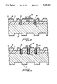
- FIG. 1 is a schematic diagram of the embodiment of the present invention employing a solderable stud in a via.
- FIG. 2 is a schematic diagram of the embodiment of the present invention employing a tapered blind via filled with solder.
- FIG. 3 is a schematic diagram of the embodiment of the present invention employing a tapered blind via partially filled with solder.
- FIG. 4 is a schematic diagram of the embodiment of the present invention employing a tapered blind via having walls plated with a metallic layer.
- FIG. 5 is a schematic diagram of the embodiment of the present invention obtained by laser drilling.
- FIG. 6 is a top view of the embodiment of the present invention employing a blind via having a top land with "air-escape" for enhanced solderability.
- the present invention is concerned with providing electrical interconnections between metallic layers on different or opposing surfaces of a dielectric substrate and especially for circuit boards and circuit cards, and most especially for power plane circuit cards.
- a widely employed technique for preparing such is to impregnate a woven fiberglass sheet with a resin composition and then laminate a metallic layer such as a copper sheet to both sides of the resin impregnated fiberglass sheet. Next, an electrical circuit is etched into the copper on one side of the sheet. Electrical interconnection is then made between the circuit on the one side and the metallic layer on the opposite side of the sheet or dielectric substrate to supply current to the circuit from the opposite side.
- epoxy resin laminated impregnated glass fabrics are widely used in the preparation of printed circuit boards and cards.
- other polymers can be used in place of the epoxy resin.
- Such polymers include halogenated polymeric materials such as polytetrafluoroethylene, and cyanate resins.
- power supply modules consist of a number of components surface mounted onto a circuitized card.
- the card consists of a thick copper plate (either 20 or 40 mil), a thin layer of the epoxy-fiberglass dielectric (one or two plies of prepreg), and typically three ounce copper circuitry.
- epoxy compositions employed therein and preferred for use in the present invention contain:
- the brominated epoxy polymers i.e., tetrabrominated diglycidyl ether of a phenol
- the brominated epoxy polymers are known and commercially available.
- the brominated epoxy polymers have an epoxy equivalent of about 455 to about 500.
- a more typical polyepoxide has a functionality of about 2, an epoxide equivalent weight about 455 to 500, and a bromine content of about 19% to 23% by weight. It is supplied by the Ciba-Geigy under the trade name Araldite 8011 as a solution containing 75% epoxy resin by weight in methyl ethyl ketone or by Dow Chemical Co. under the trade name DER-511 as an 80% solution in methyl ethyl ketone.
- epoxy polymer having functionality of about 3.5 to about 6 examples include epoxidized phenolic novolak polymers.
- the epoxidized novolak polymers are commercially available and can be prepared by known methods by the reaction of a thermoplastic phenolic aldehyde of a phenol with a halo-epoxy alkane.
- a typical epoxidized novolak that can be employed is represented by the formula: ##STR1## wherein n is at least about 1.5, wherein each R 2 individually is H or alkyl such as methyl or ethyl.
- a specific example of an epoxidized novolak is a cresolformaldehyde novolak, available under the trade designation Araldite 1280 from Ciba-Geigy.
- the zinc oxide powder employed can be present in any of the various particle shapes available, with the more typical shape being spherical.
- the particle size of the zinc oxide can vary over a wide range.
- the zinc oxide particles employed typically have a particle size such that 100% passes through a 44 micron screen.
- the zinc oxide can be employed in amounts of about 40 to about 75, more typically about 40 to about 60, and specifically about 50 parts by weight per 100 parts of resin solids.
- fillers other than zinc oxide that provide thermal enhancement without total electrical conduction including non-conducting metal oxides and metal nitrides such as Al 2 O 3 , TiO 2 , BN and AlN can be used in place of the zinc oxide.
- dicyandiamide cyanoquanidine
- a suitable solvent such as ethylene glycol monomethyl ether.
- compositions also contain as a catalyst for the cure a tertiary amine.
- Suitable tertiary amines are benzyldimethylamine, ⁇ -methyl-benzyldimethylamine, dimethylaminomethylphenol, and tris (dimethylaminomethylphenol), with N,N,N',N'-tetramethyl-1,3-butane diamine being most typical.
- the amine is usually employed in amounts of about 0.2 to about 0.4 and preferably about 0.3 parts per 100 parts by weight of the resin solids.
- Solvents are desirably employed to achieve the desired consistency or viscosity for the compositions. Usually about 90 to about 100 parts by weight of solvent per 100 parts by weight of resin solids are employed. The amount of solvent is usually such that the composition without the zinc oxide has a specific gravity of 0.9 to 1.2.
- Ethylene glycol monomethyl ether and methyl ethyl ketone serve as typical solvents. While ethylene glycol monomethyl ether and methyl ethyl ketone are the solvents of choice, other suitable solvents may also be used. For example, acetone or acetone and water may be used. Additionally, methyl ethyl ketone-dimethyl formamide can be used advantageously.
- the epoxy compositions are used to impregnate woven glass fabric from which multilayer laminates, referred to as prepregs, are prepared.
- the prepreg is prepared using the type of equipment disclosed in U.S. Pat. No. 3,523,037, disclosure of which is incorporated herein by reference.
- the process with the above epoxy composition employs temperatures of about 230° F. to about 300° F. to remove the solvents.
- the curing temperature after solvent removal is about 300° F. to about 350° F.
- the now impregnated fabric or prepreg is divided into sheets of a desired size in preparation for lamination to form the printed circuit card or board.
- two sheets of prepreg are employed. Because of the enhanced thermal conductivity of the laminate the ability to form thicker laminates with good conductivity is possible (e.g.--up to about 18 mils maximum) with a typical two prepreg sheets of a total post lamination thickness of about 4 to 6 mils being most often used.
- one to five sheets are interweaved between sheets of electrolytic copper foil or other conductive material and placed between platens of a laminating press.
- the typical copper being about 0.5 to about 5-ounce with preferred copper being 3-ounce copper about 4 mils thick as the top layer and about 0.5 to about 50 ounce copper, typically about 28 ounce copper as the bottom layer.
- the platens are cored for steam or super-heated water so that they can be heated to a temperature of 350° or more.
- the above assembly is subjected to pressure which may vary from 50 psi to 800 psi.
- the laminate is maintained at this temperature and pressure for a time sufficient to cause flow of the resin and completes the curing of the resin to a degree where it will provide properties desired in the laminate. Typical cure times vary from 30 minutes to 120 minutes at 340° F.
- circuits can be etched to the conductive layer using techniques well-known to form circuit boards.
- the electrical interconnections between the metallic layers on opposite sides of the dielectric substrate can be made pursuant to the present invention.
- numeral 1 represents the dielectric substrate (prepreg) such as of the type discussed above having a metallic layer 2 such as copper of about 0.5 to 5-ounce with about 3-ounce to about 2-ounce copper being more typical on the top surface thereof in a predetermined circuit pattern and a bottom layer of a relatively thick metallic material (3) such as copper of about a 28 ounce copper layer to provide a power plane integrated circuit card or board.
- a via (4) is provided through layers 1, 2 and 3. In the case of a through-hole the via extends all the way through the combined layers and in the case of a blind via the via stops short of extending through the entire thickness of metallic layer (3).
- a solderable metal stud (5) is placed within via (4) and extends through layer (2), substrate (1) and partially into layer (3). It is preferred that the stud (5) not protrude through the board or card because of subsequent assembly and reworking handling requirements. However, if the stud does protrude, the excess portion can be removed such as by cutting. In the case of a through hole via, the stud (5) includes flange portions (6) that extend on the top of metallic layer (2).
- an eyelet having a hollow portion such as within the vicinity of its center can be used.
- an eyelet in the case of a blind via is preferred since the hollow portion allows for the escape of gas during solder reflow.
- the stud or eyelet can be precoated with a typical solder (7) such as a 63% tin-37% lead solder or a solder 54% Sn, 26% Pb, 20% In.
- solder can be screen printed into the via prior to placing the stud or eyelet therein.
- solder joint is achieved during a solder reflow operation which can employ vapor phase, hot belt or infrared as examples.
- the studs (5) act as a bridge between the top side (2) and backside (3) current carrying metallic layer.
- the solder connection formed at each metallic layer makes both the electrical connection required and also provides for thermal dissipation.
- the solder pursuant to the present invention is not required to either adhere to or bridge the unplated/unseeded prepreg as required in prior art techniques.
- the stud (5) acts as the bridge or capillary for the solder in the via.
- the stud or eyelet can be employed without the use of solder by using a press fit into the board.
- the press fit can be accomplished by placing the stud or eyelet into a preformed hole in the board or by nailing the stud or eyelet into the board.
- the stud or eyelet can be ribbed or tapered to aid in achieving a press fit in a preformed hole.
- the above technique provides for a reliable and cost effective means for achieving the necessary interconnections between the metallic layers (2) and (3).
- the stud or eyelet can be made of any conductive and malleable metal, metal mixture or alloy such as copper, nickel, gold, brass and phosphorous-bronze.
- the material for the stud or eyelet is preferably solderable.
- the stud or eyelet is sized to fit the desired hole diameter which is generally about 10 mil to about 150 mil with about 43 mil being exemplary.
- the breadth of such flange portion is generally at least about 2 mils greater than the diameter of the hole.
- FIG. 2 facilitates an understanding of the embodiment of the present invention employing a tapered blind via containing solder.
- numeral 10 represents the dielectric substrate
- numeral 11 represents the metallic circuitry on the top surface of the substrate which can include copper.
- Further electrical conductive layer of nickel or gold (13) can be provided on the copper circuitry and a chip (15) can be provided as shown.
- the chip (15) can be placed over a blind via and connected by solder into a blind via as shown in FIG. 1 if desired.
- Blind vias (16) having tapered portion (17) are provided through metallic layer (11), dielectric substrate (10) and partially through metallic layer (12).
- the angle of tapering of the vias is about 45° to about 180° and preferably about 130°.
- the entire tapered portion is preferably contained in metallic layer (12) to provide enhanced surface tension to the solder during solder reflow process since the bottom of the hole should be wettable by the solder.
- the tapered portion provides for greater surface area.
- Solder paste is then provided by screen printing into the vias. Since the vias are preferably eccentric to the contact pads of the layer (12) the via will not be completely filled. Normally, the vias are drilled with a 10-150 mil drill bit, a specific example being a 0.05 inch drill bit, a little off center of the contact pad.
- the solder paste is then dried at usual temperatures of about 105° C. to about 130° C. and cause to reflow through vapor phase, infrared, hot belt or hot plate reflow processing.
- FIG. 3 illustrates a modification of the embodiment of FIG. 2 whereby the screen printing of the blind vias with the solder occurs by employing offset screening process to fill the via except for portion represented by numeral 18 which remains unfilled due to the offset screening procedure.
- the offset screening facilitates outgasses and hot air to escape thereby assuring for the integrity and continuity of the solder connection.
- partially solder filled blind vias pursuant to this aspect of the present invention have successfully completed at least 2000 cycles of accelerated thermal cycling (-5° C. to 150° C.) (three life cycle).
- Typical holes include those about 15 ⁇ 2 mils deep to about 30 ⁇ 2 mils deep. A specific example being bout 21 ⁇ 2 mils deep, about 43 mils wide with about a 10 mil deep tapered portion.
- FIG. 4 illustrates a further modification of the embodiment illustrated in FIG. 2 whereby vias are plated with a metal such as copper, aluminum or a precious metal such as gold, by well known plating techniques to provide a layer (20) on walls of the via.
- a metal such as copper, aluminum or a precious metal such as gold
- the plating provides a further assurance of the continuity of the electrical connections achieved pursuant to the present invention.
- the hole within the vicinity of the bottom will be free from metal in order that the bottom, which is solder wettable, be exposed.
- a laminate is provided containing a dielectric substrate of the type discussed above (30) normally about 1 to about 10 mils thick laminated between a relatively thick or heavy metallic layer (31) such as 28 ounce copper and a layer (32) of metallic material such as about 1 to about 10 ounces of copper typically about 3 ounce copper.
- the thickness of layer (32) as will become apparent below must be sufficient that upon subsequent subjection to the laser will melt and ball up and in doing so coat the sides of the via previously formed by laser drilling.
- the desired circuitry is provided on the copper layer (32) by well known photolithographic techniques.
- a window is etched through layer (32) and through dielectric substrate (30) where desired by laser.
- a typical laser being a yitrium aluminum garnet (YAG) laser.
- the energy of a YAG laser is about 2 joules/pulse operating at a 1.06 ⁇ fundamental frequency at a 10 nanosecond pulse, preferably a pulsed laser.
- Other lasers include neodymium-YAG and CO 2 .
- YAG laser is used for drilling the via and CO 2 laser for melting the copper or metal. After the hole is etched through copper layer (32) and dielectric layer (30), the laser is then used to melt and ball the metal edges (33) of the holes which in turn will then coat the walls of the via including the walls adjacent the dielectric substrate. Next, solder can be provided in the holes to thereby insure complete interconnection between the layers (31) and (32).
- the neodymium-YAG laser is preferably operated at a wavelength of 1.06 ⁇ m, and the CO 2 laser is preferably operated at a wavelength of 9.6 or 10.6 ⁇ m.
- the lasers are typically operated at a power range of 0.1 joules/cm 2 to about 2.0 joules/cm 2 .
- When the laser is pulsed such is typically carried out at about 30 picoseconds to about 10 nanoseconds.
- the particular power and pulse rate employed will depend upon the metal employed, its melting point and thickness as can be determined by persons skilled in the art without undue experimentation.
- the metal is to be melted and not vaporized.
- a 30 picosecond pulse of 0.5 joules/cm 2 melts a total depth of copper of about 1000 angstroms.
- Metals other than copper such as aluminum, gold, lead, tin, nickel and silver and combinations including lead-tin and lead-tin-indium alloys can be used, if desired.
- FIG. 6 is a top view of an embodiment of the present invention wherein the top land has an "air-escape".
- numeral 40 represents the blind via located through copper landpad 41 through the underlying substrate (not shown). Cut-out portion 42 providing for escape of air during the solder fill process. Solder mask 43 is provided.
- Through holes and blind vias are drilled into a composite having a copper layer of about 0.0042 ⁇ 0.004 inches thick on a dielectric epoxy prepreg of about 0.0052 ⁇ 0.0008 inches thick which in turn is present on thick copper substrate of about 0.04 inches thick.
- the sizes of the holes are as follows:
- each of the blind vias is tapered at a 130° angle.
- a 63/37 lead-tin solder paste is provided into the drilled holes through a solder stencil of about 0.010 inches thick.
- Ribbed eyelets are press fitted into the solder paste filled holes as follows:
- Each of the eyelets includes a flange at the upper end of about 0.063 inches.
- the solder paste is then dried by heating at about 110° C.
- the solder paste can be subjected to reflow when connection is required by exposure to infrared light.
- Example 1 is repeated except that the holes are plated with a layer of about 0.0005 inches to 0.001 inches of copper by the process discussed below.
- the substrate is degreased by contacting with an alkaline cleaner followed by a spray rinse with water.
- the substrate is microetched with sodium persulfate, following by spray rinse with H 2 O and acid dip with 25% HCl.
- the substrate is then sensitized/actuated with a composition containing about 50-60 grams/liter of SnCl 2 dihydrate, about 0.5 grams/liter of palladium chloride and about 200-300 ml/liter of 37% HCl followed by a deionized water spray rinse.
- a thin copper layer is provided from an electroless copper plating bath containing copper sulfate; EDTA, formaldehyde, KOH and KCN.
- the copper is then plated up to the desired thickness from an acid copper plating bath of CuSO 4 , H 2 SO 2 , HCl and Scherring levelers and brighteners.
- Through holes and blind vias are drilled as in example 1 and a solder stencil is placed in the drilled composite offset form normal with about 40% to about 50% of the holes on the composite being exposed to the solder paste.
- the apertures in the solder stencil are about 0.030 inches 0.054 inches to fill the 0.030 inch to 0.050 inch diameter holes.
- the solder paste is screened into the holes using a squeegee with the stencil opening of 0.054 inches oriented in the direction of the squeegee motion.
- the solder paste is dried by heating at about 110° C.
- the solder paste is caused to reflow by infrared, whereby, 100% partial hole fill is obtained.
- the partial hole fill varies from about 20-99% of the hole volume depending upon the specific hole is enhanced by reducing the effective copper land solderable surface size relative to the hole size by providing a non-solder wettable solder mask by curtain coating namely Probimer 601 from Ciba-Geigy.
- the coating is about 1 to about 2 mils thick.
- the substrate Prior to coating with the Probimer 601, the substrate is precleaned employing an alkaline degreaser such as HL-41 followed by a microetch with sodium persulfate and then contact with Entek.
- the Probimer 601 coating is exposed through a mask with a contact printer using ultraviolet radiation in the range of 365-435 nanometers at an energy level of 1000 millejoules.
- the pattern is developed by spraying with--butyrolactone for about 1.3 minutes.
- the coating is then baked in an oven at 85° C. employing a 4 minute rise, an 8 minute dwell time, and a 4 minute fall.
- the copper land size for a hole of 0.043 inch diameter and 0.021 inch depth centered in the copper land contains a solder mask window 0.064 inch square centered on the center of the hole.
- Example 3 is repeated except that the dull locations are offset from the central location of the land of about 0.010 inch.
- the process results in about 35% of the holes being partially filled with solder after the reflow operation.
- Example 1 is repeated except that 63/37 solder rings ranging from 0.040 inch to 0.050 inch diameter are used instead of the solder paste. The results obtained are similar to those of example 1.
- Example 1 is repeated except that 63/37 solder balls are used instead of the solder paste.
- the solder balls are placed in the vias and tamped in place prior to reflow to prevent loss due to rolling out of the holes.
- the results are similar to those of example 1.
Landscapes
- Engineering & Computer Science (AREA)
- Manufacturing & Machinery (AREA)
- Microelectronics & Electronic Packaging (AREA)
- Printing Elements For Providing Electric Connections Between Printed Circuits (AREA)
- Cooling Or The Like Of Electrical Apparatus (AREA)
Abstract
Description
______________________________________
           Diameter    Depth
Hole Number
           (inches)    (inches) Type
______________________________________
1          0.050       .025     blind
2           .050       .047     through
3          0.050       .017     blind
4          0.043       .025     blind
5          0.043       .017     blind
______________________________________
______________________________________
Eyelet Sizes
Diameter        Depth    Corresponding Hole
(inches)        (inches) Number
______________________________________
0.044           0.020    1
0.044           0.043    2
0.044           0.020    3
0.030           0.015    4
0.030           0.015    5
______________________________________
Claims (9)
Priority Applications (2)
| Application Number | Priority Date | Filing Date | Title |
|---|---|---|---|
| US07/598,466 US5189261A (en) | 1990-10-09 | 1990-10-09 | Electrical and/or thermal interconnections and methods for obtaining such |
| JP3238908A JPH04247677A (en) | 1990-10-09 | 1991-08-27 | Electrically/thermally interconnected circuit board and manufacture thereof |
Applications Claiming Priority (1)
| Application Number | Priority Date | Filing Date | Title |
|---|---|---|---|
| US07/598,466 US5189261A (en) | 1990-10-09 | 1990-10-09 | Electrical and/or thermal interconnections and methods for obtaining such |
Publications (1)
| Publication Number | Publication Date |
|---|---|
| US5189261A true US5189261A (en) | 1993-02-23 |
Family
ID=24395660
Family Applications (1)
| Application Number | Title | Priority Date | Filing Date |
|---|---|---|---|
| US07/598,466 Expired - Fee Related US5189261A (en) | 1990-10-09 | 1990-10-09 | Electrical and/or thermal interconnections and methods for obtaining such |
Country Status (2)
| Country | Link |
|---|---|
| US (1) | US5189261A (en) |
| JP (1) | JPH04247677A (en) |
Cited By (34)
| Publication number | Priority date | Publication date | Assignee | Title |
|---|---|---|---|---|
| US5542175A (en) * | 1994-12-20 | 1996-08-06 | International Business Machines Corporation | Method of laminating and circuitizing substrates having openings therein |
| WO1997012504A1 (en) * | 1995-09-29 | 1997-04-03 | Intel Corporation | Method for surface mounting a heatsink to a printed circuit board |
| US5736679A (en) * | 1995-12-26 | 1998-04-07 | International Business Machines Corporation | Deformable interconnect structure for connecting an internal plane to a through-hole in a multilayer circuit board |
| WO1998020539A1 (en) * | 1996-11-08 | 1998-05-14 | W.L. Gore & Associates, Inc. | Method for preparing vias for subsequent metallization |
| US5769989A (en) * | 1995-09-19 | 1998-06-23 | International Business Machines Corporation | Method and system for reworkable direct chip attach (DCA) structure with thermal enhancement |
| FR2775553A1 (en) * | 1998-03-02 | 1999-09-03 | Valeo Electronique | CONNECTION OF A POINT OF AN ELECTRONIC CARD WITH A PRINTED CIRCUIT ON A METAL SUBSTRATE WHICH CARRIES SAID CARD |
| US6003225A (en) * | 1997-12-01 | 1999-12-21 | Hughes Electronics Corporation | Fabrication of aluminum-backed printed wiring boards with plated holes therein |
| US6023029A (en) * | 1998-03-19 | 2000-02-08 | International Business Machines Corporation | Use of blind vias for soldered interconnections between substrates and printed wiring boards |
| EP1014764A1 (en) * | 1998-12-23 | 2000-06-28 | Lucas Industries Limited | Printed circuit device |
| US6106923A (en) * | 1997-05-20 | 2000-08-22 | Fujitsu Limited | Venting hole designs for multilayer conductor-dielectric structures |
| US6262477B1 (en) | 1993-03-19 | 2001-07-17 | Advanced Interconnect Technologies | Ball grid array electronic package |
| US6273327B1 (en) * | 1999-06-16 | 2001-08-14 | Trw Inc. | Apparatus and method for depositing solder material onto a circuit board |
| EP1092248A4 (en) * | 1998-05-28 | 2001-08-22 | Osram Sylvania Inc | Pcb to metallic ground connection method |
| US6381838B1 (en) * | 1997-08-12 | 2002-05-07 | Samsung Electronics Co., Ltd. | BGA package and method of manufacturing the same |
| US6411516B1 (en) * | 2001-06-15 | 2002-06-25 | Hughes Electronics Corporation | Copper slug pedestal for a printed circuit board |
| US20030102161A1 (en) * | 2001-02-20 | 2003-06-05 | International Business Machines Corporation | Structure and method for replacing an electrical net |
| US6644983B2 (en) | 2001-02-09 | 2003-11-11 | International Business Machines Corporation | Contact assembly, connector assembly utilizing same, and electronic assembly |
| US6662443B2 (en) | 1999-03-24 | 2003-12-16 | Fujitsu Limited | Method of fabricating a substrate with a via connection |
| US20030234117A1 (en) * | 2002-06-25 | 2003-12-25 | Poglitsch Lawrence R. | Ground connector assembly with substrate strain relief and method of making same |
| US20040231886A1 (en) * | 2003-05-20 | 2004-11-25 | Boggs David W. | PCB design and method for providing vented blind vias |
| US20050103820A1 (en) * | 2001-12-21 | 2005-05-19 | Hilderink Johannes Hermannus L.A. | Solder ring for production of vacuum tube and method for the production of such a solder ring and of a vacuum tube |
| US20060097379A1 (en) * | 2004-11-10 | 2006-05-11 | Chung-Cheng Wang | Substrate for electrical device and methods for making the same |
| US7121840B1 (en) | 2002-06-05 | 2006-10-17 | Magnecomp Corporation | Suspension with no-solder, no-resin conductor extending through insulator-spaced metal layers |
| EP1833101A2 (en) * | 2006-03-06 | 2007-09-12 | Samsung Electro-mechanics Co., Ltd | Backlight unit equipped with light emitting diodes |
| US20080284535A1 (en) * | 2006-10-31 | 2008-11-20 | Nihon Dempa Kogyo Co., Ltd. | Two-level mounting board and crystal oscillator using the same |
| US20110094103A1 (en) * | 2009-10-22 | 2011-04-28 | Silverbrook Research Pty Ltd | Method of fabricating inkjet printhed having low-loss contact for thermal actuators |
| US20110242765A1 (en) * | 2010-03-31 | 2011-10-06 | Hong Kong Applied Science and Technology Research Institute Company Limited | Semiconductor package and method of manufacturing the same |
| US8339743B2 (en) | 2006-06-22 | 2012-12-25 | Dai Nippon Printing Co., Ltd. | Substrate for suspension, and production process thereof |
| FR2995496A1 (en) * | 2012-09-10 | 2014-03-14 | Valeo Sys Controle Moteur Sas | Electrical circuit for use in inverter in electric compressor, has metal substrate, and metal base plate presenting barb that is inserted in perforation, where barb is allowed to come into contact with metal substrate |
| EP3258749A1 (en) * | 2016-06-17 | 2017-12-20 | Miyoshi Electronics Corporation | Electronic circuit apparatus |
| US10285282B2 (en) | 2017-07-14 | 2019-05-07 | International Business Machines Corporation | Conductive polymers within drilled holes of printed circuit boards |
| WO2019145077A1 (en) * | 2018-01-23 | 2019-08-01 | Robert Bosch Gmbh | Circuit substrate arrangement with improved electrical contact |
| US20190296454A1 (en) * | 2018-03-21 | 2019-09-26 | Te Connectivity Germany Gmbh | Connection Assembly For Connecting A Thin Conductor Piece To A Thick Conductor Piece |
| EP4175322A4 (en) * | 2020-06-25 | 2023-12-06 | FUJIFILM Corporation | Piezoelectric element |
Families Citing this family (1)
| Publication number | Priority date | Publication date | Assignee | Title |
|---|---|---|---|---|
| JP2008027570A (en) * | 2006-06-22 | 2008-02-07 | Dainippon Printing Co Ltd | Suspension substrate and manufacturing method thereof |
Citations (34)
| Publication number | Priority date | Publication date | Assignee | Title |
|---|---|---|---|---|
| US2912746A (en) * | 1955-10-10 | 1959-11-17 | Erie Resistor Corp | Method of making printed circuit panels |
| US2912745A (en) * | 1955-08-25 | 1959-11-17 | Erie Resistor Corp | Method of making a printed circuit |
| US3268652A (en) * | 1963-11-12 | 1966-08-23 | Western Electric Co | Electrical circuit assemblies |
| US3346950A (en) * | 1965-06-16 | 1967-10-17 | Ibm | Method of making through-connections by controlled punctures |
| US3445929A (en) * | 1966-08-03 | 1969-05-27 | Nicholas L Wolf | Method of connecting a terminal to a printed circuit panel |
| US3452149A (en) * | 1967-10-30 | 1969-06-24 | Fred J Rinaldi | Flexible electrical connector |
| US3501831A (en) * | 1968-06-17 | 1970-03-24 | Rogers Corp | Eyelet |
| US3562009A (en) * | 1967-02-14 | 1971-02-09 | Western Electric Co | Method of providing electrically conductive substrate through-holes |
| US3649806A (en) * | 1970-12-16 | 1972-03-14 | Dieter Konig | Process and apparatus for material excavation by beam energy |
| US3674914A (en) * | 1968-02-09 | 1972-07-04 | Photocircuits Corp | Wire scribed circuit boards and method of manufacture |
| US3673680A (en) * | 1970-12-14 | 1972-07-04 | California Computer Products | Method of circuit board with solder coated pattern |
| US3718968A (en) * | 1969-02-14 | 1973-03-06 | Atomic Energy Commission | Method for connecting a wire to a component |
| US3744129A (en) * | 1972-02-09 | 1973-07-10 | Rogers Corp | Method of forming a bus bar |
| US3880486A (en) * | 1973-03-05 | 1975-04-29 | Epis Corp | Apparatus and system for interconnecting circuits and electronic components |
| US3971610A (en) * | 1974-05-10 | 1976-07-27 | Technical Wire Products, Inc. | Conductive elastomeric contacts and connectors |
| US3980367A (en) * | 1975-03-19 | 1976-09-14 | Sealectro Corporation | Electrical connector for joining conductors attached to printed circuit boards |
| US4097684A (en) * | 1971-12-20 | 1978-06-27 | Kollmorgen Technologies Inc. | Electric wiring assemblies |
| US4121044A (en) * | 1975-06-03 | 1978-10-17 | Siemens Aktiengesellschaft | Flexible through-contacted printed circuits |
| US4323593A (en) * | 1979-04-11 | 1982-04-06 | Matsushita Electric Industrial Co., Ltd. | Method of printing a spot pattern in a printed circuit board |
| US4338506A (en) * | 1979-09-07 | 1982-07-06 | Motorola, Inc. | Method of trimming thick film capacitor |
| US4341942A (en) * | 1978-10-31 | 1982-07-27 | International Business Machines Corporation | Method of bonding wires to passivated chip microcircuit conductors |
| US4472238A (en) * | 1983-12-05 | 1984-09-18 | E. I. Du Pont De Nemours And Company | Process using plasma for forming conductive through-holes through a dielectric layer |
| US4587395A (en) * | 1982-12-06 | 1986-05-06 | The Welding Institute | Bonding leads to semiconductor devices |
| US4700473A (en) * | 1986-01-03 | 1987-10-20 | Motorola Inc. | Method of making an ultra high density pad array chip carrier |
| US4720322A (en) * | 1987-04-13 | 1988-01-19 | Texas Instruments Incorporated | Plasma etching of blind vias in printed wiring board dielectric |
| US4729061A (en) * | 1985-04-29 | 1988-03-01 | Advanced Micro Devices, Inc. | Chip on board package for integrated circuit devices using printed circuit boards and means for conveying the heat to the opposite side of the package from the chip mounting side to permit the heat to dissipate therefrom |
| US4747211A (en) * | 1987-02-09 | 1988-05-31 | Sheldahl, Inc. | Method and apparatus for preparing conductive screened through holes employing metallic plated polymer thick films |
| US4791239A (en) * | 1986-05-30 | 1988-12-13 | Furukawa Denki Kogyo Kabushiki Kaisha | Multilayer printed wiring board and method for producing the same |
| US4814578A (en) * | 1985-06-24 | 1989-03-21 | The United States Of America As Represented By The Department Of Energy | Planarization of metal films for multilevel interconnects |
| US4851614A (en) * | 1987-05-22 | 1989-07-25 | Compaq Computer Corporation | Non-occluding mounting hole with solder pad for printed circuit boards |
| US4879156A (en) * | 1986-05-02 | 1989-11-07 | International Business Machines Corporation | Multilayered ceramic substrate having solid non-porous metal conductors |
| US4888450A (en) * | 1981-12-11 | 1989-12-19 | At&T Bell Laboratories | Circuit board fabrication leading to increased capacity |
| US4935584A (en) * | 1988-05-24 | 1990-06-19 | Tektronix, Inc. | Method of fabricating a printed circuit board and the PCB produced |
| US4972050A (en) * | 1989-06-30 | 1990-11-20 | Kollmorgen Corporation | Wire scribed circuit boards and methods of their manufacture |
Family Cites Families (6)
| Publication number | Priority date | Publication date | Assignee | Title |
|---|---|---|---|---|
| JPS54156167A (en) * | 1978-05-31 | 1979-12-08 | Matsushita Electric Industrial Co Ltd | Method of producing double side printed circuit board |
| JPS56122190A (en) * | 1980-02-29 | 1981-09-25 | Matsushita Electric Works Ltd | Electric circuit board unit |
| JPS56122189A (en) * | 1980-02-29 | 1981-09-25 | Matsushita Electric Works Ltd | Electric circuit board unit |
| JPS5843595A (en) * | 1981-09-09 | 1983-03-14 | 住友電気工業株式会社 | Metallic core printed circuit board |
| JPS6355877A (en) * | 1986-08-26 | 1988-03-10 | 富士電機株式会社 | Method of jointing sheet coil |
| JPH01106496A (en) * | 1987-10-20 | 1989-04-24 | Asahi Chem Ind Co Ltd | Manufacture of through-hole circuit board |
-
1990
- 1990-10-09 US US07/598,466 patent/US5189261A/en not_active Expired - Fee Related
-
1991
- 1991-08-27 JP JP3238908A patent/JPH04247677A/en active Pending
Patent Citations (34)
| Publication number | Priority date | Publication date | Assignee | Title |
|---|---|---|---|---|
| US2912745A (en) * | 1955-08-25 | 1959-11-17 | Erie Resistor Corp | Method of making a printed circuit |
| US2912746A (en) * | 1955-10-10 | 1959-11-17 | Erie Resistor Corp | Method of making printed circuit panels |
| US3268652A (en) * | 1963-11-12 | 1966-08-23 | Western Electric Co | Electrical circuit assemblies |
| US3346950A (en) * | 1965-06-16 | 1967-10-17 | Ibm | Method of making through-connections by controlled punctures |
| US3445929A (en) * | 1966-08-03 | 1969-05-27 | Nicholas L Wolf | Method of connecting a terminal to a printed circuit panel |
| US3562009A (en) * | 1967-02-14 | 1971-02-09 | Western Electric Co | Method of providing electrically conductive substrate through-holes |
| US3452149A (en) * | 1967-10-30 | 1969-06-24 | Fred J Rinaldi | Flexible electrical connector |
| US3674914A (en) * | 1968-02-09 | 1972-07-04 | Photocircuits Corp | Wire scribed circuit boards and method of manufacture |
| US3501831A (en) * | 1968-06-17 | 1970-03-24 | Rogers Corp | Eyelet |
| US3718968A (en) * | 1969-02-14 | 1973-03-06 | Atomic Energy Commission | Method for connecting a wire to a component |
| US3673680A (en) * | 1970-12-14 | 1972-07-04 | California Computer Products | Method of circuit board with solder coated pattern |
| US3649806A (en) * | 1970-12-16 | 1972-03-14 | Dieter Konig | Process and apparatus for material excavation by beam energy |
| US4097684A (en) * | 1971-12-20 | 1978-06-27 | Kollmorgen Technologies Inc. | Electric wiring assemblies |
| US3744129A (en) * | 1972-02-09 | 1973-07-10 | Rogers Corp | Method of forming a bus bar |
| US3880486A (en) * | 1973-03-05 | 1975-04-29 | Epis Corp | Apparatus and system for interconnecting circuits and electronic components |
| US3971610A (en) * | 1974-05-10 | 1976-07-27 | Technical Wire Products, Inc. | Conductive elastomeric contacts and connectors |
| US3980367A (en) * | 1975-03-19 | 1976-09-14 | Sealectro Corporation | Electrical connector for joining conductors attached to printed circuit boards |
| US4121044A (en) * | 1975-06-03 | 1978-10-17 | Siemens Aktiengesellschaft | Flexible through-contacted printed circuits |
| US4341942A (en) * | 1978-10-31 | 1982-07-27 | International Business Machines Corporation | Method of bonding wires to passivated chip microcircuit conductors |
| US4323593A (en) * | 1979-04-11 | 1982-04-06 | Matsushita Electric Industrial Co., Ltd. | Method of printing a spot pattern in a printed circuit board |
| US4338506A (en) * | 1979-09-07 | 1982-07-06 | Motorola, Inc. | Method of trimming thick film capacitor |
| US4888450A (en) * | 1981-12-11 | 1989-12-19 | At&T Bell Laboratories | Circuit board fabrication leading to increased capacity |
| US4587395A (en) * | 1982-12-06 | 1986-05-06 | The Welding Institute | Bonding leads to semiconductor devices |
| US4472238A (en) * | 1983-12-05 | 1984-09-18 | E. I. Du Pont De Nemours And Company | Process using plasma for forming conductive through-holes through a dielectric layer |
| US4729061A (en) * | 1985-04-29 | 1988-03-01 | Advanced Micro Devices, Inc. | Chip on board package for integrated circuit devices using printed circuit boards and means for conveying the heat to the opposite side of the package from the chip mounting side to permit the heat to dissipate therefrom |
| US4814578A (en) * | 1985-06-24 | 1989-03-21 | The United States Of America As Represented By The Department Of Energy | Planarization of metal films for multilevel interconnects |
| US4700473A (en) * | 1986-01-03 | 1987-10-20 | Motorola Inc. | Method of making an ultra high density pad array chip carrier |
| US4879156A (en) * | 1986-05-02 | 1989-11-07 | International Business Machines Corporation | Multilayered ceramic substrate having solid non-porous metal conductors |
| US4791239A (en) * | 1986-05-30 | 1988-12-13 | Furukawa Denki Kogyo Kabushiki Kaisha | Multilayer printed wiring board and method for producing the same |
| US4747211A (en) * | 1987-02-09 | 1988-05-31 | Sheldahl, Inc. | Method and apparatus for preparing conductive screened through holes employing metallic plated polymer thick films |
| US4720322A (en) * | 1987-04-13 | 1988-01-19 | Texas Instruments Incorporated | Plasma etching of blind vias in printed wiring board dielectric |
| US4851614A (en) * | 1987-05-22 | 1989-07-25 | Compaq Computer Corporation | Non-occluding mounting hole with solder pad for printed circuit boards |
| US4935584A (en) * | 1988-05-24 | 1990-06-19 | Tektronix, Inc. | Method of fabricating a printed circuit board and the PCB produced |
| US4972050A (en) * | 1989-06-30 | 1990-11-20 | Kollmorgen Corporation | Wire scribed circuit boards and methods of their manufacture |
Cited By (52)
| Publication number | Priority date | Publication date | Assignee | Title |
|---|---|---|---|---|
| US6262477B1 (en) | 1993-03-19 | 2001-07-17 | Advanced Interconnect Technologies | Ball grid array electronic package |
| US5542175A (en) * | 1994-12-20 | 1996-08-06 | International Business Machines Corporation | Method of laminating and circuitizing substrates having openings therein |
| US5769989A (en) * | 1995-09-19 | 1998-06-23 | International Business Machines Corporation | Method and system for reworkable direct chip attach (DCA) structure with thermal enhancement |
| WO1997012504A1 (en) * | 1995-09-29 | 1997-04-03 | Intel Corporation | Method for surface mounting a heatsink to a printed circuit board |
| US5779134A (en) * | 1995-09-29 | 1998-07-14 | Intel Corporation | Method for surface mounting a heatsink to a printed circuit board |
| US5736679A (en) * | 1995-12-26 | 1998-04-07 | International Business Machines Corporation | Deformable interconnect structure for connecting an internal plane to a through-hole in a multilayer circuit board |
| WO1998020539A1 (en) * | 1996-11-08 | 1998-05-14 | W.L. Gore & Associates, Inc. | Method for preparing vias for subsequent metallization |
| US6106923A (en) * | 1997-05-20 | 2000-08-22 | Fujitsu Limited | Venting hole designs for multilayer conductor-dielectric structures |
| US6381838B1 (en) * | 1997-08-12 | 2002-05-07 | Samsung Electronics Co., Ltd. | BGA package and method of manufacturing the same |
| US6003225A (en) * | 1997-12-01 | 1999-12-21 | Hughes Electronics Corporation | Fabrication of aluminum-backed printed wiring boards with plated holes therein |
| FR2775553A1 (en) * | 1998-03-02 | 1999-09-03 | Valeo Electronique | CONNECTION OF A POINT OF AN ELECTRONIC CARD WITH A PRINTED CIRCUIT ON A METAL SUBSTRATE WHICH CARRIES SAID CARD |
| WO1999045754A1 (en) * | 1998-03-02 | 1999-09-10 | Valeo Vision | Connecting an electronic card point to a printed circuit on a metal substrate bearing said card |
| US6023029A (en) * | 1998-03-19 | 2000-02-08 | International Business Machines Corporation | Use of blind vias for soldered interconnections between substrates and printed wiring boards |
| US6452116B2 (en) | 1998-03-19 | 2002-09-17 | International Business Machines Corporation | Use of blind vias for soldered interconnections between substrates and printed wiring boards |
| EP1092248A4 (en) * | 1998-05-28 | 2001-08-22 | Osram Sylvania Inc | Pcb to metallic ground connection method |
| US6423910B1 (en) * | 1998-12-23 | 2002-07-23 | Lucas Industries Limited | Printed circuit device |
| EP1014764A1 (en) * | 1998-12-23 | 2000-06-28 | Lucas Industries Limited | Printed circuit device |
| US6662443B2 (en) | 1999-03-24 | 2003-12-16 | Fujitsu Limited | Method of fabricating a substrate with a via connection |
| US6273327B1 (en) * | 1999-06-16 | 2001-08-14 | Trw Inc. | Apparatus and method for depositing solder material onto a circuit board |
| US6644983B2 (en) | 2001-02-09 | 2003-11-11 | International Business Machines Corporation | Contact assembly, connector assembly utilizing same, and electronic assembly |
| US20030102161A1 (en) * | 2001-02-20 | 2003-06-05 | International Business Machines Corporation | Structure and method for replacing an electrical net |
| US6705006B2 (en) * | 2001-02-20 | 2004-03-16 | International Business Machines Corporation | Method for replacing an electrical net on a printed circuit board |
| US6411516B1 (en) * | 2001-06-15 | 2002-06-25 | Hughes Electronics Corporation | Copper slug pedestal for a printed circuit board |
| US20050103820A1 (en) * | 2001-12-21 | 2005-05-19 | Hilderink Johannes Hermannus L.A. | Solder ring for production of vacuum tube and method for the production of such a solder ring and of a vacuum tube |
| US7121840B1 (en) | 2002-06-05 | 2006-10-17 | Magnecomp Corporation | Suspension with no-solder, no-resin conductor extending through insulator-spaced metal layers |
| US20030234117A1 (en) * | 2002-06-25 | 2003-12-25 | Poglitsch Lawrence R. | Ground connector assembly with substrate strain relief and method of making same |
| US6740824B2 (en) | 2002-06-25 | 2004-05-25 | Motorola, Inc. | Ground connector assembly with substrate strain relief and method of making same |
| US20040231886A1 (en) * | 2003-05-20 | 2004-11-25 | Boggs David W. | PCB design and method for providing vented blind vias |
| US20060097379A1 (en) * | 2004-11-10 | 2006-05-11 | Chung-Cheng Wang | Substrate for electrical device and methods for making the same |
| US7786567B2 (en) * | 2004-11-10 | 2010-08-31 | Chung-Cheng Wang | Substrate for electrical device and methods for making the same |
| EP1833101A2 (en) * | 2006-03-06 | 2007-09-12 | Samsung Electro-mechanics Co., Ltd | Backlight unit equipped with light emitting diodes |
| EP2170024B1 (en) * | 2006-03-06 | 2017-08-09 | Samsung Electronics Co., Ltd. | Backlight unit equipped with light emitting diodes |
| US8339743B2 (en) | 2006-06-22 | 2012-12-25 | Dai Nippon Printing Co., Ltd. | Substrate for suspension, and production process thereof |
| US20080284535A1 (en) * | 2006-10-31 | 2008-11-20 | Nihon Dempa Kogyo Co., Ltd. | Two-level mounting board and crystal oscillator using the same |
| US7791425B2 (en) * | 2006-10-31 | 2010-09-07 | Nihon Dempa Kogyo Co., Ltd. | Two-level mounting board and crystal oscillator using the same |
| US20110094103A1 (en) * | 2009-10-22 | 2011-04-28 | Silverbrook Research Pty Ltd | Method of fabricating inkjet printhed having low-loss contact for thermal actuators |
| US8453329B2 (en) * | 2009-10-22 | 2013-06-04 | Zamtec Ltd | Method of fabricating inkjet printhead having low-loss contact for thermal actuators |
| US20110242765A1 (en) * | 2010-03-31 | 2011-10-06 | Hong Kong Applied Science and Technology Research Institute Company Limited | Semiconductor package and method of manufacturing the same |
| US8248803B2 (en) * | 2010-03-31 | 2012-08-21 | Hong Kong Applied Science and Technology Research Institute Company Limited | Semiconductor package and method of manufacturing the same |
| FR2995496A1 (en) * | 2012-09-10 | 2014-03-14 | Valeo Sys Controle Moteur Sas | Electrical circuit for use in inverter in electric compressor, has metal substrate, and metal base plate presenting barb that is inserted in perforation, where barb is allowed to come into contact with metal substrate |
| EP3258749A1 (en) * | 2016-06-17 | 2017-12-20 | Miyoshi Electronics Corporation | Electronic circuit apparatus |
| US10285282B2 (en) | 2017-07-14 | 2019-05-07 | International Business Machines Corporation | Conductive polymers within drilled holes of printed circuit boards |
| US10334741B2 (en) | 2017-07-14 | 2019-06-25 | International Business Machines Corporation | Conductive polymers within drilled holes of printed circuit boards |
| US10750622B2 (en) | 2017-07-14 | 2020-08-18 | International Business Machines Corporation | Conductive polymers within drilled holes of printed circuit boards |
| US10772215B2 (en) | 2017-07-14 | 2020-09-08 | International Business Machines Corporation | Conductive polymers within drilled holes of printed circuit boards |
| WO2019145077A1 (en) * | 2018-01-23 | 2019-08-01 | Robert Bosch Gmbh | Circuit substrate arrangement with improved electrical contact |
| CN111602237A (en) * | 2018-01-23 | 2020-08-28 | 罗伯特·博世有限公司 | Line base unit with improved electrical contact |
| US11071203B2 (en) | 2018-01-23 | 2021-07-20 | Robert Bosch Gmbh | Circuit substrate arrangement with improved electrical contact |
| CN111602237B (en) * | 2018-01-23 | 2023-09-26 | 罗伯特·博世有限公司 | Line base device with improved electrical contacts |
| US20190296454A1 (en) * | 2018-03-21 | 2019-09-26 | Te Connectivity Germany Gmbh | Connection Assembly For Connecting A Thin Conductor Piece To A Thick Conductor Piece |
| US10892568B2 (en) * | 2018-03-21 | 2021-01-12 | Te Connectivity Germany Gmbh | Connection assembly for connecting a thin conductor piece to a thick conductor piece |
| EP4175322A4 (en) * | 2020-06-25 | 2023-12-06 | FUJIFILM Corporation | Piezoelectric element |
Also Published As
| Publication number | Publication date |
|---|---|
| JPH04247677A (en) | 1992-09-03 |
Similar Documents
| Publication | Publication Date | Title |
|---|---|---|
| US5189261A (en) | Electrical and/or thermal interconnections and methods for obtaining such | |
| EP0964610B1 (en) | Printed wiring board and process for forming it | |
| US6138350A (en) | Process for manufacturing a circuit board with filled holes | |
| US5243142A (en) | Printed wiring board and process for producing the same | |
| US5418689A (en) | Printed circuit board or card for direct chip attachment and fabrication thereof | |
| US7049528B2 (en) | Semiconductor chip mounting wiring board, manufacturing method for same, and semiconductor module | |
| US6869750B2 (en) | Structure and method for forming a multilayered structure | |
| US7514298B2 (en) | Printed wiring board for mounting semiconductor | |
| US20130033827A1 (en) | Electrically conductive adhesive (eca) for multilayer device interconnects | |
| KR19990068179A (en) | Semiconductor plastic package, metal plate for said package, and method of producing copper-clad board for said package | |
| US20020119396A1 (en) | Structure and method for forming z-laminated multilayered packaging substrate | |
| WO2007097440A1 (en) | Printed wiring board and process for producing the same | |
| US7910156B2 (en) | Method of making circuitized substrate with selected conductors having solder thereon | |
| JP2011100908A (en) | Printed wiring board, and semiconductor device | |
| US7629559B2 (en) | Method of improving electrical connections in circuitized substrates | |
| JP4582938B2 (en) | Insulating sheet manufacturing method and wiring board manufacturing method | |
| JP2001217356A (en) | Multilayer circuit board and semiconductor device | |
| JP4055026B2 (en) | Manufacturing method of build-up multilayer printed wiring board | |
| JP2002204057A (en) | Multilayer printed wiring board and method of manufacturing the same | |
| JP3944801B2 (en) | Manufacturing method of semiconductor mounting substrate | |
| JP2001135750A (en) | Method for manufacturing semiconductor package substrate | |
| JPH1187930A (en) | Manufacture of multilayered printed circuit board | |
| JP3944802B2 (en) | Manufacturing method of semiconductor mounting substrate | |
| JP4301152B2 (en) | Via hole forming metal clad laminate and through hole forming unclad plate | |
| JP4975913B2 (en) | Multilayer printed circuit board |
Legal Events
| Date | Code | Title | Description |
|---|---|---|---|
| AS | Assignment |
Owner name: INTERNATIONAL BUSINESS MACHINES CORPORATION, NEW Y Free format text: ASSIGNMENT OF ASSIGNORS INTEREST.;ASSIGNORS:ALEXANDER, LAWRENCE C.;APPELT, BERND K.;BALKIN, DAVID K.;AND OTHERS;REEL/FRAME:005506/0183;SIGNING DATES FROM 19900914 TO 19901001 |
|
| FPAY | Fee payment |
Year of fee payment: 4 |
|
| FEPP | Fee payment procedure |
Free format text: PAYOR NUMBER ASSIGNED (ORIGINAL EVENT CODE: ASPN); ENTITY STATUS OF PATENT OWNER: LARGE ENTITY |
|
| FPAY | Fee payment |
Year of fee payment: 8 |
|
| REMI | Maintenance fee reminder mailed | ||
| LAPS | Lapse for failure to pay maintenance fees | ||
| STCH | Information on status: patent discontinuation |
Free format text: PATENT EXPIRED DUE TO NONPAYMENT OF MAINTENANCE FEES UNDER 37 CFR 1.362 |
|
| FP | Lapsed due to failure to pay maintenance fee |
Effective date: 20050223 |