US4978419A - Process for defining vias through silicon nitride and polyamide - Google Patents
Process for defining vias through silicon nitride and polyamide Download PDFInfo
- Publication number
- US4978419A US4978419A US07/205,009 US20500988A US4978419A US 4978419 A US4978419 A US 4978419A US 20500988 A US20500988 A US 20500988A US 4978419 A US4978419 A US 4978419A
- Authority
- US
- United States
- Prior art keywords
- layer
- silicon nitride
- photoresist
- polyimide
- depositing
- Prior art date
- Legal status (The legal status is an assumption and is not a legal conclusion. Google has not performed a legal analysis and makes no representation as to the accuracy of the status listed.)
- Expired - Fee Related
Links
Images

Classifications
-
- H—ELECTRICITY
- H01—ELECTRIC ELEMENTS
- H01L—SEMICONDUCTOR DEVICES NOT COVERED BY CLASS H10
- H01L21/00—Processes or apparatus adapted for the manufacture or treatment of semiconductor or solid state devices or of parts thereof
- H01L21/70—Manufacture or treatment of devices consisting of a plurality of solid state components formed in or on a common substrate or of parts thereof; Manufacture of integrated circuit devices or of parts thereof
- H01L21/71—Manufacture of specific parts of devices defined in group H01L21/70
- H01L21/768—Applying interconnections to be used for carrying current between separate components within a device comprising conductors and dielectrics
- H01L21/76801—Applying interconnections to be used for carrying current between separate components within a device comprising conductors and dielectrics characterised by the formation and the after-treatment of the dielectrics, e.g. smoothing
- H01L21/76802—Applying interconnections to be used for carrying current between separate components within a device comprising conductors and dielectrics characterised by the formation and the after-treatment of the dielectrics, e.g. smoothing by forming openings in dielectrics
- H01L21/76804—Applying interconnections to be used for carrying current between separate components within a device comprising conductors and dielectrics characterised by the formation and the after-treatment of the dielectrics, e.g. smoothing by forming openings in dielectrics by forming tapered via holes
-
- H—ELECTRICITY
- H01—ELECTRIC ELEMENTS
- H01L—SEMICONDUCTOR DEVICES NOT COVERED BY CLASS H10
- H01L21/00—Processes or apparatus adapted for the manufacture or treatment of semiconductor or solid state devices or of parts thereof
- H01L21/02—Manufacture or treatment of semiconductor devices or of parts thereof
- H01L21/04—Manufacture or treatment of semiconductor devices or of parts thereof the devices having at least one potential-jump barrier or surface barrier, e.g. PN junction, depletion layer or carrier concentration layer
- H01L21/18—Manufacture or treatment of semiconductor devices or of parts thereof the devices having at least one potential-jump barrier or surface barrier, e.g. PN junction, depletion layer or carrier concentration layer the devices having semiconductor bodies comprising elements of Group IV of the Periodic System or AIIIBV compounds with or without impurities, e.g. doping materials
- H01L21/30—Treatment of semiconductor bodies using processes or apparatus not provided for in groups H01L21/20 - H01L21/26
- H01L21/31—Treatment of semiconductor bodies using processes or apparatus not provided for in groups H01L21/20 - H01L21/26 to form insulating layers thereon, e.g. for masking or by using photolithographic techniques; After treatment of these layers; Selection of materials for these layers
- H01L21/3105—After-treatment
- H01L21/311—Etching the insulating layers by chemical or physical means
- H01L21/31105—Etching inorganic layers
- H01L21/31111—Etching inorganic layers by chemical means
- H01L21/31116—Etching inorganic layers by chemical means by dry-etching
-
- H—ELECTRICITY
- H01—ELECTRIC ELEMENTS
- H01L—SEMICONDUCTOR DEVICES NOT COVERED BY CLASS H10
- H01L21/00—Processes or apparatus adapted for the manufacture or treatment of semiconductor or solid state devices or of parts thereof
- H01L21/02—Manufacture or treatment of semiconductor devices or of parts thereof
- H01L21/04—Manufacture or treatment of semiconductor devices or of parts thereof the devices having at least one potential-jump barrier or surface barrier, e.g. PN junction, depletion layer or carrier concentration layer
- H01L21/18—Manufacture or treatment of semiconductor devices or of parts thereof the devices having at least one potential-jump barrier or surface barrier, e.g. PN junction, depletion layer or carrier concentration layer the devices having semiconductor bodies comprising elements of Group IV of the Periodic System or AIIIBV compounds with or without impurities, e.g. doping materials
- H01L21/30—Treatment of semiconductor bodies using processes or apparatus not provided for in groups H01L21/20 - H01L21/26
- H01L21/31—Treatment of semiconductor bodies using processes or apparatus not provided for in groups H01L21/20 - H01L21/26 to form insulating layers thereon, e.g. for masking or by using photolithographic techniques; After treatment of these layers; Selection of materials for these layers
- H01L21/3105—After-treatment
- H01L21/311—Etching the insulating layers by chemical or physical means
- H01L21/31127—Etching organic layers
- H01L21/31133—Etching organic layers by chemical means
- H01L21/31138—Etching organic layers by chemical means by dry-etching
-
- H—ELECTRICITY
- H01—ELECTRIC ELEMENTS
- H01L—SEMICONDUCTOR DEVICES NOT COVERED BY CLASS H10
- H01L21/00—Processes or apparatus adapted for the manufacture or treatment of semiconductor or solid state devices or of parts thereof
- H01L21/02—Manufacture or treatment of semiconductor devices or of parts thereof
- H01L21/04—Manufacture or treatment of semiconductor devices or of parts thereof the devices having at least one potential-jump barrier or surface barrier, e.g. PN junction, depletion layer or carrier concentration layer
- H01L21/18—Manufacture or treatment of semiconductor devices or of parts thereof the devices having at least one potential-jump barrier or surface barrier, e.g. PN junction, depletion layer or carrier concentration layer the devices having semiconductor bodies comprising elements of Group IV of the Periodic System or AIIIBV compounds with or without impurities, e.g. doping materials
- H01L21/30—Treatment of semiconductor bodies using processes or apparatus not provided for in groups H01L21/20 - H01L21/26
- H01L21/31—Treatment of semiconductor bodies using processes or apparatus not provided for in groups H01L21/20 - H01L21/26 to form insulating layers thereon, e.g. for masking or by using photolithographic techniques; After treatment of these layers; Selection of materials for these layers
- H01L21/3105—After-treatment
- H01L21/311—Etching the insulating layers by chemical or physical means
- H01L21/31144—Etching the insulating layers by chemical or physical means using masks
Definitions
- This invention is related to a process for defining vias through polyimide and silicon nitride layers for making circuit interconnections in an integrated circuit.
- VLSI very large scale integrated circuits
- contact metal layer 10 is sequentially covered by a layer 12 of silicon nitride and then a layer 14 of polyimide
- vias 16 through both of these layers to make circuit interconnections with additional metal layers that are subsequently deposited.
- the following process can be used to simultaneously define vias through a polyimide and silicon nitride layer:
- a substrate having a first layer of silicon nitride and a second layer of polyimide
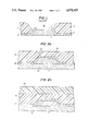
- FIG. 1 is a cross-sectional view of a semiconductor chip showing a prior art method of defining vias through two insulating layers.
- FIGS. 2A-E are cross-sectional views of a semiconductor chip showing the process steps for defining vias through two insulating layers according to this invention.
- FIG. 2A A cross-sectional view of a portion of a semiconductor chip is shown schematically in FIG. 2A.
- Substrate 20 represents that portion of the semiconductor chip that has been processed prior to the deposition of metal, or other types of device interconnect lines.
- first level metallurgy 22 already deposited on substrate 20 are the first level metallurgy 22.
- the metal chosen for first level metallurgy 22 is not critical to this invention and can be any metal that is commonly used for this purpose. It is very common to design VLSI circuits in which several levels of interconnect metallurgy are required. To eliminate short circuits between metal levels, insulation or passivation layers are deposited between the metal levels.
- a thin conformal layer of silicon nitride 24 approximately 0.2-1.0 microns thick is first deposited over substrate 20 and metal lines 22.
- the method used to deposit the silicon nitride can include chemical vapor deposition, or any other technique commonly used for this purpose.
- a planarizing layer of polyimide 26 is deposited on top of silicon nitride layer 24, a planarizing layer of polyimide 26 is deposited.
- the polyimide can be spun or sprayed on as is well-known in the art with a thickness in the range of 0.4-2.5 microns.
- first level metal 22 In order to make electrical contact between first level metal 22 and a subsequent level of metal (not shown) it is necessary to define a via through silicon nitride layer 24 and polyimide layer 26 with a profile as shown by dotted lines 28. The gradual slope of the via is necessary in order to ensure continuous metal coverage.
- the first step in the via definition process is the deposition of a layer of photoresist 28 as seen in FIG. 2B.
- the thickness of the photoresist layer 28 is preferably in the range 1.0 to 2.5 microns.
- the choice of photoresist is likewise not critical but should be one that is capable of producing an image having a negative profile as shown in FIG. 2C, and is relatively etch resistant.
- a positive photoresist with an additive such as imidazole has been used with excellent results.
- the photoresist layer 28 is exposed to radiation through a mask (not shown) as conventionally done, and then developed, leaving the structure as shown in FIG. 2C.
- the polyimide layer 26 is reactive ion etched with the following process conditions:
- the resulting structure is shown in FIG. 2D.
- the via through silicon nitride layer 24 is next defined with another reactive ion etch process with the following parameters:
- the final structure after resist strip is shown in FIG. 2E. Due to the negligible organic etch rate with the CF 4 /H 2 process conditions, the dimensions and the profile of the polyimide are maintained. The final structure is now ready for the deposition of a second level of metal.
- a first level of interconnection metallurgy was formed and patterned.
- a blanket layer of Si 3 N 4 was next deposited using plasma enhanced chemical vapor deposition.
- the nominal thickness of the Si 3 N 4 was approximately 0.4 microns.
- a layer of polyimide was spun-on over the Si 3 N 4 layer and baked at 350° C. for 30 minutes.
- the nominal thickness of the polyimide layer 0.6 microns to 1.3 microns due to the non-uniform underlying topography and planarizing effects of the polyimide layer.
- a layer of positive diazonovolak-based photoresist containing 1% by weight imidazole as an image reversal additive was spun-on and baked to a final thickness of approximately 2.2 microns.
- the photoresist was then exposed to UV light through a mask having a pattern of contacts.
- the exposed photoresist was then baked for 25 minutes at 100 degrees C.
- the baked resist was then blanket exposed to UV radiation at an intensity of approximately 880-1400 mj/cm 2 .
- the exposed pattern was then developed using 0.23N KOH as well-known in the art.
- the polyimide layer and Si 3 N 4 layer were etched in a reactive ion etcher using the etching parameters previously described to open up self-aligned contact holes to the underlying layers.
Abstract
A process for defining vias through a polyimide and silicon nitride layer is disclosed. After the deposition of a first layer of silicon nitride and a second layer of polyimide, a layer of photoresist capable of producing negatively sloped walls is then lithographically defined with a pattern of vias. After the photoresist is developed, the polyimide layer is etched with a CF4 O2 gas mixture using the developed photoresist layer as etch mask. The silicon nitride layer is then etched with a CF4 /H2 gas mixture using the etched polyimide layer as an etch mask.
Description
This application is a continuation-in-part of Ser. No. 917,350, filed 10/9/86, now abandoned.
1. Technical Field
This invention is related to a process for defining vias through polyimide and silicon nitride layers for making circuit interconnections in an integrated circuit.
2. Background Art
In the fabrication of very large scale integrated circuits (VLSI), it is sometimes necessary to make circuit interconnections between layers of metallization which are separated by one or more layers of insulating material. In the case of an integrated circuit as shown in FIG. 1 in which contact metal layer 10 is sequentially covered by a layer 12 of silicon nitride and then a layer 14 of polyimide, it is necessary to define vias 16 through both of these layers to make circuit interconnections with additional metal layers that are subsequently deposited.
It is known in the art to define vias using the following process steps: (1) apply photoresist layer; (2) lithographically define the via pattern; and (3) etch the underlying layer with an appropriate wet or dry etchant. When necessary to define vias through two layers, the above process steps are repeated for the second layer.
The problem, however, is that with the tolerances inherent in current technologies, it is very difficult to align the vias in each of the respective layers. To ensure that the vias do coincide to the extent necessary for adequate metallization, it is necessary to make the vias in each layer significantly larger than what would ordinarily be necessary as seen in FIG. 1. In VLSI applications, this would consume a large amount of real estate on a semiconductor chip.
It is therefore desirable to have a process for defining vias through both a silicon nitride and a polyimide layer in a self-aligned manner such that the wasted space on the chip is avoided.
It is an object of this invention to provide a process for defining vias through a silicon nitride and polyimide layer.
It is an additional object to provide a process for defining vias through a silicon nitride and polyimide layer such that the vias are self-aligned so that no unnecessary chip area is used.
It is a further object to provide a process for defining vias through a silicon nitride and polyimide layer wherein only one masking and lithographic step is required, thereby reducing the number of process steps necessary.
In accordance with these objects, the following process can be used to simultaneously define vias through a polyimide and silicon nitride layer:
1. Provide a substrate having a first layer of silicon nitride and a second layer of polyimide;
2. Deposit a layer of photoresist capable of producing negatively sloped profiles;
3. Lithographically define a pattern of vias in the photoresist;
4. Develop the photoresist to produce a pattern of vias having negatively sloped profiles;
5. Etch the polyimide layer using the developed photoresist layer as an etch mask with a CF4 /O2 gas mixture; and
6. Etch the silicon nitride layer using the etched polyimide layer as an etch mask with a CF4 /H2 gas mixture.
The foregoing and other advantages of the invention will be more fully understood with reference to the description of the best mode and the drawing wherein:
FIG. 1 is a cross-sectional view of a semiconductor chip showing a prior art method of defining vias through two insulating layers.
FIGS. 2A-E are cross-sectional views of a semiconductor chip showing the process steps for defining vias through two insulating layers according to this invention.
A cross-sectional view of a portion of a semiconductor chip is shown schematically in FIG. 2A. Substrate 20, represents that portion of the semiconductor chip that has been processed prior to the deposition of metal, or other types of device interconnect lines. Already deposited on substrate 20 are the first level metallurgy 22. The metal chosen for first level metallurgy 22 is not critical to this invention and can be any metal that is commonly used for this purpose. It is very common to design VLSI circuits in which several levels of interconnect metallurgy are required. To eliminate short circuits between metal levels, insulation or passivation layers are deposited between the metal levels. In this best mode, a thin conformal layer of silicon nitride 24 approximately 0.2-1.0 microns thick is first deposited over substrate 20 and metal lines 22. The method used to deposit the silicon nitride can include chemical vapor deposition, or any other technique commonly used for this purpose. On top of silicon nitride layer 24, a planarizing layer of polyimide 26 is deposited. The polyimide can be spun or sprayed on as is well-known in the art with a thickness in the range of 0.4-2.5 microns.
In order to make electrical contact between first level metal 22 and a subsequent level of metal (not shown) it is necessary to define a via through silicon nitride layer 24 and polyimide layer 26 with a profile as shown by dotted lines 28. The gradual slope of the via is necessary in order to ensure continuous metal coverage.
The first step in the via definition process is the deposition of a layer of photoresist 28 as seen in FIG. 2B. The thickness of the photoresist layer 28 is preferably in the range 1.0 to 2.5 microns. The choice of photoresist is likewise not critical but should be one that is capable of producing an image having a negative profile as shown in FIG. 2C, and is relatively etch resistant. A positive photoresist with an additive such as imidazole has been used with excellent results.
Still looking at FIG. 2C, the photoresist layer 28 is exposed to radiation through a mask (not shown) as conventionally done, and then developed, leaving the structure as shown in FIG. 2C.
Using the developed photoresist layer 28 as an etch mask, the polyimide layer 26 is reactive ion etched with the following process conditions:
Power density--0.10 watts per centimeter square
CF4 mass flow rate--6-10 sccm
O2 mass flow rate--85-100 sccm
Pressure--25-40 mtorr
The resulting structure is shown in FIG. 2D. The via through silicon nitride layer 24 is next defined with another reactive ion etch process with the following parameters:
Power density--0.25 watts per centimeter square
CF4 mass flow rate--80-83 sccm
H2 mass flow rate--15-19 sccm
Pressure--20-35 mtorr
The final structure after resist strip is shown in FIG. 2E. Due to the negligible organic etch rate with the CF4 /H2 process conditions, the dimensions and the profile of the polyimide are maintained. The final structure is now ready for the deposition of a second level of metal.
Following the fabrication of semiconductor devices on a substrate, a first level of interconnection metallurgy was formed and patterned. A blanket layer of Si3 N4 was next deposited using plasma enhanced chemical vapor deposition. The nominal thickness of the Si3 N4 was approximately 0.4 microns.
A layer of polyimide was spun-on over the Si3 N4 layer and baked at 350° C. for 30 minutes. The nominal thickness of the polyimide layer 0.6 microns to 1.3 microns due to the non-uniform underlying topography and planarizing effects of the polyimide layer.
Following the polyimide deposition, a layer of positive diazonovolak-based photoresist containing 1% by weight imidazole as an image reversal additive was spun-on and baked to a final thickness of approximately 2.2 microns. The photoresist was then exposed to UV light through a mask having a pattern of contacts. The exposed photoresist was then baked for 25 minutes at 100 degrees C. The baked resist was then blanket exposed to UV radiation at an intensity of approximately 880-1400 mj/cm2. The exposed pattern was then developed using 0.23N KOH as well-known in the art.
Using the developed photoresist layer as an etch mask, the polyimide layer and Si3 N4 layer were etched in a reactive ion etcher using the etching parameters previously described to open up self-aligned contact holes to the underlying layers.
While the invention has been shown with reference to a best mode, it would be obvious to one skilled in the art that the process can be used for defining vias through polyimide and silicon nitride for other applications without departing from the spirit and scope of the invention. Therefore, the invention should only be limited as specified in the claims.
Claims (4)
1. In an integrated circuit chip having a plurality of semiconductor devices, a process for defining self-aligned vias through a silicon nitride layer and a polyimide layer comprising the following steps in the following order:
depositing a layer of silicon nitride over said semiconductor devices, said silicon nitride layer having a thickness in the range 0.2-1.0 microns;
depositing a layer of polyimide over said silicon nitride layer, said polyimide layer having a thickness greater than said silicon nitride layer and being in the range 0.6-2.5 microns;
depositing a layer of photoresist capable of forming sidewalls having a negative profile over said polyimide layer, said layer of photoresist having a thickness greater than said polyimide layer;
patternwise exposing said photoresist layer to radiation;
developing the exposed photoresist layer to form an image having negatively sloped sidewalls;
etching the silicon nitride layer with a mixture of CF4 and O2 using the patterned photoresist layer as an etch mask; and
etching the silicon nitride layer with a mixture of CF4 and H2, using the etched polyimide layer as an etch mask.
2. The process as claimed in claim 1 wherein the photoresist is a positive photoresist containing an imidazole additive.
3. A process for defining vias through a silicon nitride layer and a polyimide layer comprising the following steps in the following order:
depositing a layer of silicon nitride on a substrate, said silicon nitride layer having a thickness in the range 0.2-1.0 microns;
depositing a layer of polyimide over said silicon nitride layer, said polyimide layer having a thickness greater than said silicon nitride layer and being in the range 0.6-2.5 microns;
depositing a layer of photoresist capable of forming sidewalls having a negative profile over said polyimide layer, said layer of photoresist having a thickness greater than said polyimide layer;
lithographically defining an image in said photoresist layer having negatively sloped sidewalls;
etching the polyimide layer with a mixture of CF4 and O2 using the photoresist layer as an etch mask; and
etching the silicon nitride layer with a mixture of CF4 and H2, using the etched polyimide layer as an etch mask.
4. The process as claimed in claim 3 wherein the photoresist is a positive photoresist containing an imidazole additive.
Applications Claiming Priority (1)
| Application Number | Priority Date | Filing Date | Title |
|---|---|---|---|
| US91735086A | 1986-10-09 | 1986-10-09 |
Related Parent Applications (1)
| Application Number | Title | Priority Date | Filing Date |
|---|---|---|---|
| US07917350 Continuation-In-Part | 1988-10-09 |
Publications (1)
| Publication Number | Publication Date |
|---|---|
| US4978419A true US4978419A (en) | 1990-12-18 |
Family
ID=25438667
Family Applications (1)
| Application Number | Title | Priority Date | Filing Date |
|---|---|---|---|
| US07/205,009 Expired - Fee Related US4978419A (en) | 1986-10-09 | 1988-05-31 | Process for defining vias through silicon nitride and polyamide |
Country Status (4)
| Country | Link |
|---|---|
| US (1) | US4978419A (en) |
| EP (1) | EP0263348B1 (en) |
| JP (1) | JPS63104425A (en) |
| DE (1) | DE3780743T2 (en) |
Cited By (22)
| Publication number | Priority date | Publication date | Assignee | Title |
|---|---|---|---|---|
| GB2260643A (en) * | 1991-10-16 | 1993-04-21 | Samsung Electronics Co Ltd | Method for interconnecting layers in a semiconductor device |
| US5266530A (en) * | 1991-11-08 | 1993-11-30 | Bell Communications Research, Inc. | Self-aligned gated electron field emitter |
| US5283209A (en) * | 1991-01-17 | 1994-02-01 | Alcatel N.V. | Method of localized treatment on a projection, in particular for lithographic etching on a semiconductor substrate |
| US5350486A (en) * | 1991-10-10 | 1994-09-27 | Sgs-Thomson Microelectronics, Inc. | Semiconductor planarization process |
| EP0692799A2 (en) * | 1994-07-15 | 1996-01-17 | Plessey Semiconductors Limited | Trimmable capacitor |
| US5543335A (en) * | 1993-05-05 | 1996-08-06 | Ixys Corporation | Advanced power device process for low drop |
| US5747375A (en) * | 1993-07-22 | 1998-05-05 | Sanyo Electric Co., Ltd. | Method of manufacturing a semiconductor integrated circuit device |
| US5900072A (en) * | 1995-09-02 | 1999-05-04 | Lg Semicon Co., Ltd. | Insulating layer structure for semiconductor device |
| US5976987A (en) * | 1997-10-03 | 1999-11-02 | Vlsi Technology, Inc. | In-situ corner rounding during oxide etch for improved plug fill |
| US5976766A (en) * | 1992-02-21 | 1999-11-02 | Sony Corporation | Contact hole forming method |
| US6093641A (en) * | 1997-04-24 | 2000-07-25 | Lg Semicon Co., Ltd. | Method for fabricating semiconductor device with an increased process tolerance |
| US20020030931A1 (en) * | 2000-09-11 | 2002-03-14 | Alps Electric Co., Ltd. | Thin film magnetic head having partial insulating layer formed on bottom pole layer through gap layer and method of manufacturing the same |
| US6423907B1 (en) | 1998-02-09 | 2002-07-23 | Tessera, Inc. | Components with releasable leads |
| WO2002093262A1 (en) * | 2001-05-11 | 2002-11-21 | Shipley Company, L.L.C. | Thick film photoresists and methods for use thereof |
| US6645848B2 (en) | 2001-06-01 | 2003-11-11 | Emcore Corporation | Method of improving the fabrication of etched semiconductor devices |
| US20030232504A1 (en) * | 2002-06-14 | 2003-12-18 | Aaron Eppler | Process for etching dielectric films with improved resist and/or etch profile characteristics |
| WO2004027853A1 (en) * | 2002-09-11 | 2004-04-01 | Infineon Technologies Ag | Method for structuring layers on semiconductor components and semiconductor memory |
| US20040171260A1 (en) * | 2002-06-14 | 2004-09-02 | Lam Research Corporation | Line edge roughness control |
| US20050266612A1 (en) * | 1998-12-21 | 2005-12-01 | Mou-Shiung Lin | Top layers of metal for high performance IC's |
| US20080042298A1 (en) * | 1999-06-30 | 2008-02-21 | Atsushi Kanda | Semiconductor devices and methods of fabricating the same |
| US20100105214A1 (en) * | 2007-05-30 | 2010-04-29 | Mitsubishi Electric Corporation | Method of manufacturing semiconductor device |
| US20110177670A1 (en) * | 2010-01-20 | 2011-07-21 | International Business Machines Corporaton | Through silicon via lithographic alignment and registration |
Families Citing this family (3)
| Publication number | Priority date | Publication date | Assignee | Title |
|---|---|---|---|---|
| JPH0410420A (en) * | 1990-04-26 | 1992-01-14 | Sanyo Electric Co Ltd | Manufacture of semiconductor integrated circuit |
| GB2279804A (en) * | 1993-07-02 | 1995-01-11 | Plessey Semiconductors Ltd | Insulating layers for multilayer wiring |
| JPH09306901A (en) * | 1996-05-17 | 1997-11-28 | Nec Corp | Manufacture of semiconductor device |
Citations (12)
| Publication number | Priority date | Publication date | Assignee | Title |
|---|---|---|---|---|
| US4367119A (en) * | 1980-08-18 | 1983-01-04 | International Business Machines Corporation | Planar multi-level metal process with built-in etch stop |
| US4423547A (en) * | 1981-06-01 | 1984-01-03 | International Business Machines Corporation | Method for forming dense multilevel interconnection metallurgy for semiconductor devices |
| US4430153A (en) * | 1983-06-30 | 1984-02-07 | International Business Machines Corporation | Method of forming an RIE etch barrier by in situ conversion of a silicon containing alkyl polyamide/polyimide |
| US4447290A (en) * | 1982-06-10 | 1984-05-08 | Intel Corporation | CMOS Process with unique plasma etching step |
| US4487652A (en) * | 1984-03-30 | 1984-12-11 | Motorola, Inc. | Slope etch of polyimide |
| US4495220A (en) * | 1983-10-07 | 1985-01-22 | Trw Inc. | Polyimide inter-metal dielectric process |
| US4497684A (en) * | 1983-02-22 | 1985-02-05 | Amdahl Corporation | Lift-off process for depositing metal on a substrate |
| US4519872A (en) * | 1984-06-11 | 1985-05-28 | International Business Machines Corporation | Use of depolymerizable polymers in the fabrication of lift-off structure for multilevel metal processes |
| US4523976A (en) * | 1984-07-02 | 1985-06-18 | Motorola, Inc. | Method for forming semiconductor devices |
| US4545851A (en) * | 1983-05-09 | 1985-10-08 | Fujitsu Limited | Etching method for semiconductor devices |
| US4618878A (en) * | 1983-06-18 | 1986-10-21 | Kabushiki Kaisha Toshiba | Semiconductor device having a multilayer wiring structure using a polyimide resin |
| US4758306A (en) * | 1987-08-17 | 1988-07-19 | International Business Machines Corporation | Stud formation method optimizing insulator gap-fill and metal hole-fill |
Family Cites Families (4)
| Publication number | Priority date | Publication date | Assignee | Title |
|---|---|---|---|---|
| DE3175488D1 (en) * | 1981-02-07 | 1986-11-20 | Ibm Deutschland | Process for the formation and the filling of holes in a layer applied to a substrate |
| JPS58140139A (en) * | 1982-02-16 | 1983-08-19 | Matsushita Electric Ind Co Ltd | Semiconductor device and manufacture thereof |
| JPS59149025A (en) * | 1983-02-16 | 1984-08-25 | Hitachi Ltd | Manufacture of semiconductor device |
| JPS6237945A (en) * | 1985-08-13 | 1987-02-18 | Toshiba Corp | Manufacture of semiconductor device |
-
1987
- 1987-08-20 JP JP62205336A patent/JPS63104425A/en active Pending
- 1987-09-22 DE DE8787113825T patent/DE3780743T2/en not_active Expired - Fee Related
- 1987-09-22 EP EP87113825A patent/EP0263348B1/en not_active Expired
-
1988
- 1988-05-31 US US07/205,009 patent/US4978419A/en not_active Expired - Fee Related
Patent Citations (12)
| Publication number | Priority date | Publication date | Assignee | Title |
|---|---|---|---|---|
| US4367119A (en) * | 1980-08-18 | 1983-01-04 | International Business Machines Corporation | Planar multi-level metal process with built-in etch stop |
| US4423547A (en) * | 1981-06-01 | 1984-01-03 | International Business Machines Corporation | Method for forming dense multilevel interconnection metallurgy for semiconductor devices |
| US4447290A (en) * | 1982-06-10 | 1984-05-08 | Intel Corporation | CMOS Process with unique plasma etching step |
| US4497684A (en) * | 1983-02-22 | 1985-02-05 | Amdahl Corporation | Lift-off process for depositing metal on a substrate |
| US4545851A (en) * | 1983-05-09 | 1985-10-08 | Fujitsu Limited | Etching method for semiconductor devices |
| US4618878A (en) * | 1983-06-18 | 1986-10-21 | Kabushiki Kaisha Toshiba | Semiconductor device having a multilayer wiring structure using a polyimide resin |
| US4430153A (en) * | 1983-06-30 | 1984-02-07 | International Business Machines Corporation | Method of forming an RIE etch barrier by in situ conversion of a silicon containing alkyl polyamide/polyimide |
| US4495220A (en) * | 1983-10-07 | 1985-01-22 | Trw Inc. | Polyimide inter-metal dielectric process |
| US4487652A (en) * | 1984-03-30 | 1984-12-11 | Motorola, Inc. | Slope etch of polyimide |
| US4519872A (en) * | 1984-06-11 | 1985-05-28 | International Business Machines Corporation | Use of depolymerizable polymers in the fabrication of lift-off structure for multilevel metal processes |
| US4523976A (en) * | 1984-07-02 | 1985-06-18 | Motorola, Inc. | Method for forming semiconductor devices |
| US4758306A (en) * | 1987-08-17 | 1988-07-19 | International Business Machines Corporation | Stud formation method optimizing insulator gap-fill and metal hole-fill |
Cited By (101)
| Publication number | Priority date | Publication date | Assignee | Title |
|---|---|---|---|---|
| US5283209A (en) * | 1991-01-17 | 1994-02-01 | Alcatel N.V. | Method of localized treatment on a projection, in particular for lithographic etching on a semiconductor substrate |
| US5350486A (en) * | 1991-10-10 | 1994-09-27 | Sgs-Thomson Microelectronics, Inc. | Semiconductor planarization process |
| DE4139462A1 (en) * | 1991-10-16 | 1993-04-22 | Samsung Electronics Co Ltd | METHOD FOR CONNECTING LAYERS IN A SEMICONDUCTOR DEVICE |
| GB2260643B (en) * | 1991-10-16 | 1995-05-24 | Samsung Electronics Co Ltd | Method for interconnecting layers in a semiconductor device |
| GB2260643A (en) * | 1991-10-16 | 1993-04-21 | Samsung Electronics Co Ltd | Method for interconnecting layers in a semiconductor device |
| US5266530A (en) * | 1991-11-08 | 1993-11-30 | Bell Communications Research, Inc. | Self-aligned gated electron field emitter |
| US5976766A (en) * | 1992-02-21 | 1999-11-02 | Sony Corporation | Contact hole forming method |
| US5543335A (en) * | 1993-05-05 | 1996-08-06 | Ixys Corporation | Advanced power device process for low drop |
| US5747375A (en) * | 1993-07-22 | 1998-05-05 | Sanyo Electric Co., Ltd. | Method of manufacturing a semiconductor integrated circuit device |
| EP0692799A2 (en) * | 1994-07-15 | 1996-01-17 | Plessey Semiconductors Limited | Trimmable capacitor |
| EP0692799A3 (en) * | 1994-07-15 | 1997-05-14 | Plessey Semiconductors Ltd | Trimmable capacitor |
| US5900072A (en) * | 1995-09-02 | 1999-05-04 | Lg Semicon Co., Ltd. | Insulating layer structure for semiconductor device |
| US6093641A (en) * | 1997-04-24 | 2000-07-25 | Lg Semicon Co., Ltd. | Method for fabricating semiconductor device with an increased process tolerance |
| US5976987A (en) * | 1997-10-03 | 1999-11-02 | Vlsi Technology, Inc. | In-situ corner rounding during oxide etch for improved plug fill |
| US6763579B2 (en) | 1998-02-09 | 2004-07-20 | Tessera, Inc. | Method of making components with releasable leads |
| US6423907B1 (en) | 1998-02-09 | 2002-07-23 | Tessera, Inc. | Components with releasable leads |
| US20020117329A1 (en) * | 1998-02-09 | 2002-08-29 | Belgacem Haba | Components with releasable leads |
| US7114250B2 (en) | 1998-02-09 | 2006-10-03 | Tessera, Inc. | Method of making components with releasable leads |
| US6557253B1 (en) | 1998-02-09 | 2003-05-06 | Tessera, Inc. | Method of making components with releasable leads |
| US20040217003A1 (en) * | 1998-02-09 | 2004-11-04 | Tessera, Inc. | Method of making components with releasable leads |
| US6664484B2 (en) | 1998-02-09 | 2003-12-16 | Tessera, Inc. | Components with releasable leads |
| US20080142981A1 (en) * | 1998-12-21 | 2008-06-19 | Mou-Shiung Lin | Top layers of metal for high performance IC's |
| US20070293036A1 (en) * | 1998-12-21 | 2007-12-20 | Mou-Shiung Lin | Top layers of metal for high performance IC's |
| US8531038B2 (en) | 1998-12-21 | 2013-09-10 | Megica Corporation | Top layers of metal for high performance IC's |
| US8471384B2 (en) | 1998-12-21 | 2013-06-25 | Megica Corporation | Top layers of metal for high performance IC's |
| US8415800B2 (en) | 1998-12-21 | 2013-04-09 | Megica Corporation | Top layers of metal for high performance IC's |
| US8022545B2 (en) | 1998-12-21 | 2011-09-20 | Megica Corporation | Top layers of metal for high performance IC's |
| US7999384B2 (en) | 1998-12-21 | 2011-08-16 | Megica Corporation | Top layers of metal for high performance IC's |
| US7884479B2 (en) | 1998-12-21 | 2011-02-08 | Megica Corporation | Top layers of metal for high performance IC's |
| US7863654B2 (en) | 1998-12-21 | 2011-01-04 | Megica Corporation | Top layers of metal for high performance IC's |
| US20050266612A1 (en) * | 1998-12-21 | 2005-12-01 | Mou-Shiung Lin | Top layers of metal for high performance IC's |
| US7482693B2 (en) | 1998-12-21 | 2009-01-27 | Mou-Shiung Lin | Top layers of metal for high performance IC's |
| US7465975B2 (en) | 1998-12-21 | 2008-12-16 | Mou-Shiung Lin | Top layers of metal for high performance IC's |
| US20070262458A1 (en) * | 1998-12-21 | 2007-11-15 | Mou-Shiung Lin | Top layers of metal for high performance IC's |
| US20070262455A1 (en) * | 1998-12-21 | 2007-11-15 | Mou-Shiung Lin | Top layers of metal for high performance IC's |
| US20070273041A1 (en) * | 1998-12-21 | 2007-11-29 | Mou-Shiung Lin | Top layers of metal for high performance IC's |
| US20070273039A1 (en) * | 1998-12-21 | 2007-11-29 | Mou-Shiung Lin | Top layers of metal for high performance IC's |
| US20070273040A1 (en) * | 1998-12-21 | 2007-11-29 | Mou-Shiung Lin | Top layers of metal for high performance IC's |
| US20070273036A1 (en) * | 1998-12-21 | 2007-11-29 | Mou-Shiung Lin | Top layers of metal for high performance IC's |
| US20070273037A1 (en) * | 1998-12-21 | 2007-11-29 | Mou-Shiung Lin | Top layers of metal for high performance IC's |
| US20070273035A1 (en) * | 1998-12-21 | 2007-11-29 | Mou-Shiung Lin | Top layers of metal for high performance IC's |
| US20070273038A1 (en) * | 1998-12-21 | 2007-11-29 | Mou-Shiung Lin | Top layers of metal for high performance IC's |
| US20070273034A1 (en) * | 1998-12-21 | 2007-11-29 | Mou-Shiung Lin | Top layers of metal for high performance IC's |
| US20070273032A1 (en) * | 1998-12-21 | 2007-11-29 | Mou-Shiung Lin | Top layers of metal for high performance IC's |
| US20070281467A1 (en) * | 1998-12-21 | 2007-12-06 | Mou-Shiung Lin | Top layers of metal for high performance IC's |
| US20070278690A1 (en) * | 1998-12-21 | 2007-12-06 | Mou-Shiung Lin | Top layers of metal for high performance IC's |
| US20070278689A1 (en) * | 1998-12-21 | 2007-12-06 | Mou-Shiung Lin | Top layers of metal for high performance IC's |
| US20070278691A1 (en) * | 1998-12-21 | 2007-12-06 | Mou-Shiung Lin | Top layers of metal for high performance IC's |
| US20070278684A1 (en) * | 1998-12-21 | 2007-12-06 | Mou-Shiung Lin | Top layers of metal for high performance IC's |
| US20070281463A1 (en) * | 1998-12-21 | 2007-12-06 | Mou-Shiung Lin | Top layers of metal for high performance IC's |
| US20070278687A1 (en) * | 1998-12-21 | 2007-12-06 | Mou-Shiung Lin | Top layers of metal for high performance IC's |
| US20070278685A1 (en) * | 1998-12-21 | 2007-12-06 | Mou-Shiung Lin | Top layers of metal for high performance IC's |
| US20070278679A1 (en) * | 1998-12-21 | 2007-12-06 | Mou-Shiung Lin | Top layers of metal for high performance IC's |
| US20070281468A1 (en) * | 1998-12-21 | 2007-12-06 | Mou-Shiung Lin | Top layers of metal for high performance IC's |
| US20070284752A1 (en) * | 1998-12-21 | 2007-12-13 | Mou-Shiung Lin | Top layers of metal for high performance IC's |
| US20070284739A1 (en) * | 1998-12-21 | 2007-12-13 | Mou-Shiung Lin | Top layers of metal for high performance IC's |
| US20070284753A1 (en) * | 1998-12-21 | 2007-12-13 | Mou-Shiung Lin | Top layers of metal for high performance IC's |
| US20070284751A1 (en) * | 1998-12-21 | 2007-12-13 | Mou-Shiung Lin | Top layers of metal for high performance IC's |
| US20070290356A1 (en) * | 1998-12-21 | 2007-12-20 | Mou-Shiung Lin | Top layers of metal for high performance IC's |
| US20070290355A1 (en) * | 1998-12-21 | 2007-12-20 | Mou-Shiung Lin | Top layers of metal for high performance IC's |
| US7456100B2 (en) | 1998-12-21 | 2008-11-25 | Mou-Shiung Lin | Top layers of metal for high performance IC's |
| US20070290353A1 (en) * | 1998-12-21 | 2007-12-20 | Mou-Shiung Lin | Top layers of metal for high performance IC's |
| US20070290354A1 (en) * | 1998-12-21 | 2007-12-20 | Mou-Shiung Lin | Top layers of metal for high performance IC's |
| US20070290352A1 (en) * | 1998-12-21 | 2007-12-20 | Mou-Shiung Lin | Top layers of metal for high performance IC's |
| US20070293037A1 (en) * | 1998-12-21 | 2007-12-20 | Mou-Shiung Lin | Top layers of metal for high performance IC's |
| US20070290357A1 (en) * | 1998-12-21 | 2007-12-20 | Mou-Shiung Lin | Top layers of metal for high performance IC's |
| US7442969B2 (en) | 1998-12-21 | 2008-10-28 | Mou-Shiung Lin | Top layers of metal for high performance IC's |
| US20080048329A1 (en) * | 1998-12-21 | 2008-02-28 | Mou-Shiung Lin | Top layers of metal for high performance IC's |
| US20080050913A1 (en) * | 1998-12-21 | 2008-02-28 | Mou-Shiung Lin | Top layers of metal for high performance IC's |
| US20080083987A1 (en) * | 1998-12-21 | 2008-04-10 | Mou-Shiung Lin | Top layers of metal for high performance IC's |
| US7358610B2 (en) | 1998-12-21 | 2008-04-15 | Mou-Shiung Lin | Top layers of metal for high performance IC's |
| US7382058B2 (en) | 1998-12-21 | 2008-06-03 | Mou-Shiung Lin | Top layers of metal for high performance IC's |
| US7385291B2 (en) | 1998-12-21 | 2008-06-10 | Mou-Shiung Lin | Top layers of metal for high performance IC's |
| US7385292B2 (en) | 1998-12-21 | 2008-06-10 | Mou-Shiung Lin | Top layers of metal for high performance IC's |
| US7388292B2 (en) | 1998-12-21 | 2008-06-17 | Mou-Shiung Lin | Top layers of metal for high performance IC's |
| US7425764B2 (en) | 1998-12-21 | 2008-09-16 | Mou-Shiung Lin | Top layers of metal for high performance IC's |
| US20080142980A1 (en) * | 1998-12-21 | 2008-06-19 | Mou-Shiung Lin | Top layers of metal for high performance IC's |
| US20080146020A1 (en) * | 1998-12-21 | 2008-06-19 | Mou-Shiung Lin | Top layers of metal for high performance IC's |
| US7396756B2 (en) | 1998-12-21 | 2008-07-08 | Mou-Shiung Lin | Top layers of metal for high performance IC's |
| US7397135B2 (en) | 1998-12-21 | 2008-07-08 | Mou-Shiung Lin | Top layers of metal for high performance IC's |
| US7422976B2 (en) * | 1998-12-21 | 2008-09-09 | Mou-Shiung Lin | Top layers of metal for high performance IC's |
| US20080258298A1 (en) * | 1999-06-30 | 2008-10-23 | Atsushi Kanda | Semiconductor devices and methods of fabricating the same |
| US20080042298A1 (en) * | 1999-06-30 | 2008-02-21 | Atsushi Kanda | Semiconductor devices and methods of fabricating the same |
| US20020030931A1 (en) * | 2000-09-11 | 2002-03-14 | Alps Electric Co., Ltd. | Thin film magnetic head having partial insulating layer formed on bottom pole layer through gap layer and method of manufacturing the same |
| US6999275B2 (en) * | 2000-09-11 | 2006-02-14 | Alps Electric Co., Ltd. | Thin film magnetic head having partial insulating layer formed on bottom pole layer through gap layer and method of manufacturing the same |
| US20050019705A1 (en) * | 2001-05-11 | 2005-01-27 | Shipley Company, L.L.C. | Thick film photoresists and methods for use thereof |
| US6800422B2 (en) | 2001-05-11 | 2004-10-05 | Shipley Company, L.L.C. | Thick film photoresists and methods for use thereof |
| WO2002093262A1 (en) * | 2001-05-11 | 2002-11-21 | Shipley Company, L.L.C. | Thick film photoresists and methods for use thereof |
| CN100409101C (en) * | 2001-05-11 | 2008-08-06 | 希普雷公司 | Thick film photoresists and methods for use thereof |
| US6645848B2 (en) | 2001-06-01 | 2003-11-11 | Emcore Corporation | Method of improving the fabrication of etched semiconductor devices |
| US7547635B2 (en) | 2002-06-14 | 2009-06-16 | Lam Research Corporation | Process for etching dielectric films with improved resist and/or etch profile characteristics |
| WO2003107410A2 (en) * | 2002-06-14 | 2003-12-24 | Lam Research Corporation | Process for etching dielectric films with improved resist and/or etch profile characteristics |
| US20040171260A1 (en) * | 2002-06-14 | 2004-09-02 | Lam Research Corporation | Line edge roughness control |
| US20030232504A1 (en) * | 2002-06-14 | 2003-12-18 | Aaron Eppler | Process for etching dielectric films with improved resist and/or etch profile characteristics |
| WO2003107410A3 (en) * | 2002-06-14 | 2004-04-15 | Lam Res Corp | Process for etching dielectric films with improved resist and/or etch profile characteristics |
| WO2004027853A1 (en) * | 2002-09-11 | 2004-04-01 | Infineon Technologies Ag | Method for structuring layers on semiconductor components and semiconductor memory |
| US20100105214A1 (en) * | 2007-05-30 | 2010-04-29 | Mitsubishi Electric Corporation | Method of manufacturing semiconductor device |
| US20110177670A1 (en) * | 2010-01-20 | 2011-07-21 | International Business Machines Corporaton | Through silicon via lithographic alignment and registration |
| WO2011090852A2 (en) | 2010-01-20 | 2011-07-28 | International Business Machines Corporation | Through silicon via lithographic alignment and registration |
| US8039356B2 (en) | 2010-01-20 | 2011-10-18 | International Business Machines Corporation | Through silicon via lithographic alignment and registration |
| DE112011100134T5 (en) | 2010-01-20 | 2012-10-04 | International Business Machines Corporation | Continuous silicon connection with lithographic alignment and registration |
Also Published As
| Publication number | Publication date |
|---|---|
| EP0263348A2 (en) | 1988-04-13 |
| EP0263348A3 (en) | 1988-10-05 |
| JPS63104425A (en) | 1988-05-09 |
| DE3780743T2 (en) | 1993-03-11 |
| DE3780743D1 (en) | 1992-09-03 |
| EP0263348B1 (en) | 1992-07-29 |
Similar Documents
| Publication | Publication Date | Title |
|---|---|---|
| US4978419A (en) | Process for defining vias through silicon nitride and polyamide | |
| US4721689A (en) | Method for simultaneously forming an interconnection level and via studs | |
| US4070501A (en) | Forming self-aligned via holes in thin film interconnection systems | |
| JPH01290236A (en) | Method of levelling wide trench | |
| US4661204A (en) | Method for forming vertical interconnects in polyimide insulating layers | |
| JPH0573338B2 (en) | ||
| US5109267A (en) | Method for producing an integrated circuit structure with a dense multilayer metallization pattern | |
| KR100333382B1 (en) | Method for forming multi-level metal interconnection of semiconductor device | |
| US5395796A (en) | Etch stop layer using polymers for integrated circuits | |
| EP0188735B1 (en) | Tailoring of via-hole sidewall slope in an insulating layer | |
| KR19980087292A (en) | Semiconductor device manufacturing method | |
| US20030082906A1 (en) | Via formation in polymers | |
| US20210375750A1 (en) | Interconnection structure having increased conductive features and method of manufacturing the same | |
| JPH08279488A (en) | Fabrication of semiconductor device | |
| JPH0750694B2 (en) | Conductive layer formation method | |
| US6143644A (en) | Method to prevent passivation from keyhole damage and resist extrusion | |
| US4970573A (en) | Self-planarized gold interconnect layer | |
| US6284645B1 (en) | Controlling improvement of critical dimension of dual damasceue process using spin-on-glass process | |
| KR100710193B1 (en) | Method for forming semi-conductor device | |
| KR100365745B1 (en) | Method for forming contact hole in semiconductor device | |
| JP2783898B2 (en) | Method for manufacturing semiconductor device | |
| KR100365936B1 (en) | Method for forming via contact in semiconductor device | |
| KR920000629B1 (en) | Manufacturing method of semiconductor device using etch-back process | |
| KR100290466B1 (en) | Method of manufacturing a semiconductor device | |
| KR950011553B1 (en) | Metalizing method of semiconductor device |
Legal Events
| Date | Code | Title | Description |
|---|---|---|---|
| REMI | Maintenance fee reminder mailed | ||
| FPAY | Fee payment |
Year of fee payment: 4 |
|
| SULP | Surcharge for late payment | ||
| REMI | Maintenance fee reminder mailed | ||
| LAPS | Lapse for failure to pay maintenance fees | ||
| FP | Lapsed due to failure to pay maintenance fee |
Effective date: 19981218 |
|
| STCH | Information on status: patent discontinuation |
Free format text: PATENT EXPIRED DUE TO NONPAYMENT OF MAINTENANCE FEES UNDER 37 CFR 1.362 |