US4901027A - Signal generator - Google Patents
Signal generator Download PDFInfo
- Publication number
- US4901027A US4901027A US07/284,691 US28469188A US4901027A US 4901027 A US4901027 A US 4901027A US 28469188 A US28469188 A US 28469188A US 4901027 A US4901027 A US 4901027A
- Authority
- US
- United States
- Prior art keywords
- output
- phase
- phase accumulator
- coupled
- voltage
- Prior art date
- Legal status (The legal status is an assumption and is not a legal conclusion. Google has not performed a legal analysis and makes no representation as to the accuracy of the status listed.)
- Expired - Lifetime
Links
- 238000009825 accumulation Methods 0.000 claims abstract description 8
- 230000006870 function Effects 0.000 claims description 15
- 230000000295 complement effect Effects 0.000 claims description 3
- 238000010586 diagram Methods 0.000 description 7
- 230000001360 synchronised effect Effects 0.000 description 4
- 238000002847 impedance measurement Methods 0.000 description 2
- 238000007796 conventional method Methods 0.000 description 1
- 238000001514 detection method Methods 0.000 description 1
- 230000010354 integration Effects 0.000 description 1
- 238000012986 modification Methods 0.000 description 1
- 230000004048 modification Effects 0.000 description 1
- 230000009466 transformation Effects 0.000 description 1
Images


Classifications
-
- H—ELECTRICITY
- H03—ELECTRONIC CIRCUITRY
- H03L—AUTOMATIC CONTROL, STARTING, SYNCHRONISATION OR STABILISATION OF GENERATORS OF ELECTRONIC OSCILLATIONS OR PULSES
- H03L7/00—Automatic control of frequency or phase; Synchronisation
-
- H—ELECTRICITY
- H03—ELECTRONIC CIRCUITRY
- H03B—GENERATION OF OSCILLATIONS, DIRECTLY OR BY FREQUENCY-CHANGING, BY CIRCUITS EMPLOYING ACTIVE ELEMENTS WHICH OPERATE IN A NON-SWITCHING MANNER; GENERATION OF NOISE BY SUCH CIRCUITS
- H03B27/00—Generation of oscillations providing a plurality of outputs of the same frequency but differing in phase, other than merely two anti-phase outputs
Definitions
- the present invention relates to a phase accumulation type signal generator which accumulates an amount of phase to be added (hereinafter referred to as a phase add amount), for each clock, reads data out of a waveform memory using the added output, and converts the read output into an analog signal.
- a phase add amount an amount of phase to be added
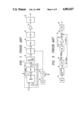
- FIG. 1 is a block diagram of a conventional phase accumulation type signal generator.
- a phase accumulator 11 a phase add amount n and the output k of a latch circuit 13 are added by an adder 12 and the added output n+k is latched in the latch circuit 13 for each clock, whereby the phase add amount n is accumulated.
- a signal of a frequency f, produced by an oscillator 14, is frequency divided by a variable frequency divider 15 down to 1/m to yield a clock, by which the latch circuit 13 is latched.
- Data is read out of a waveform memory 16 using the output of the latch circuit 13, and the read output of the waveform memory 16 is latched by the clock in a latch circuit 17.
- the output of the latch circuit 17 is converted by a D-A converter 18 into an analog signal, which is applied to a low-pass filter 19, an amplifier 21 and an attenuator 22.
- the phase accumulation type signal generator in FIG. 1 is capable of generating, with a simple arrangement, low-distortion signals of high frequency accuracy at low and even ultra-low frequencies.
- the phase add amount n does not bear an integral multiple relationship to the maximum value of the adder 12 (that is, the address space of the memory 16)
- the amount of offset of the phase (hereinafter referred to as a phase offset amount) at the time a carry is generated, will vary.
- a phase offset amount the amount of offset of the phase
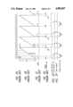
- FIG. 2A the phase add amount n is accumulated for each clock, the output of the adder 12 increases as shown in FIG. 2B, and upon generation of the clock immediately after an overflow of the adder 12, a carry is yielded as a synchronization pulse as depicted in FIG. 2C.
- the phase offset amount ⁇ of this synchronization pulse fluctuates as shown in FIG. 2D, and consequently, such a synchronization pulse cannot be employed for triggering a synchronous detection or Fourier transformation for im
- Impedance measurement calls for a sine-wave signal which is applied to a measuring object and a pulse signal which is accurately synchronized with the sine-wave signal.
- FIG. 3 shows a conventional method used to meet this requirement.
- the output of an oscillator 31 is frequency divided by a frequency divider 32, the output of which is filtered by a low-pass filter 33 to produce a sine-wave signal.
- the sine-wave signal is applied to a measuring object 34, the current output of which is converted by a current-voltage converter 35 into a voltage signal.
- the voltage signal is provided to a synchronous detector 36, wherein it is synchronously detected by the output of the frequency divider 32, and the synchronously detected output is integrated by an integrator 37.
- the filter characteristic of the low-pass filter 33 is fixed, the number of frequencies used is limited to one or several and the frequency used cannot be changed.
- the analog voltage and the ramp function voltage are compared by a comparator, which yields a synchronization pulse when they agree with each other.
- FIG. 1 is a block diagram of a conventional signal generator
- FIGS. 2A, 2B, 2C and 2D show waveforms for explaining the operation of the conventional signal generator
- FIGS. 2E and 2F are waveforms for explaining the operation of the present invention.
- FIG. 3 is a block diagram of a conventional impedance measuring apparatus
- FIG. 4 is a block diagram of an embodiment of the signal generator of the present invention.
- FIG. 5 is a block diagram of a specific operative example of a difference circuit 41 used in FIG. 4;
- FIG. 6 is a block diagram of another example of the difference circuit 41.
- FIG. 7 is a block diagram of a modified form of the signal generator of the present invention.
- FIG. 4 illustrates in block form an embodiment of the present invention, in which the parts corresponding to those in FIG. 1 are identified by the same reference numerals.
- the carry output from the adder 12 is loaded into a D-type flip-flop 42 by the clock from the frequency divider 15.
- the output of the D-type flip-flop 42 is applied to an input Sync of the difference circuit 41.
- the difference circuit 41 is supplied with the phase add amount n and the output k s of the adder 12.
- FIG. 5 shows a specific operative example of the difference circuit 41, in which the input phase add amount n thereto is converted by a D-A converter 43 into an analog voltage a 2 n, the output k s of the adder 12 is latched by the Sync input in a latch circuit 44, and the output k s of the latch circuit 44 is converted by a D-A converter 45 into an analog voltage a 2 k s , which is subtracted from the analog voltage a 2 n in an analog subtractor 46, providing a 2 (n-k s ).
- FIG. 6 shows another example of the difference circuit 41, in which the output k s of the adder 12 is reversed in sign by a NOT circuit 47 to obtain a complement k s which is provided to an adder 48, wherein it is added with the phase add amount n and 1 to obtain n+k s +1.
- the added output is latched in a latch circuit 49 by the Sync input.
- the latch output is converted by a multiplier type D-A converter 51 into the analog voltage a 2 (n-k s ).
- An inverted signal of the output of the D-type flip-flop 42 is applied to a D-type flip-flop 53 to load therein a high-level signal "1", and a low-level signal from the Q output of the D-type flip-flop 53 is applied to a reset switch 54 of the integrator 50, turning it OFF. Consequently, when the synchronization pulse, i.e. the carry shown in FIG. 2C, falls, the Q output of the flip-flop 53 goes to a "0", by which the reset switch 54 is turned OFF, and the integrator 50 starts integration as shown in FIG. 2E, yielding a ramp function voltage as follows: ##EQU1##
- the D-A converter 52 and the integrator 50 constitute a ramp function voltage generator 60.
- the ramp function voltage V(t) and the analog voltage V 1 from the difference circuit 41 are compared by a comparator 55, which yields a high-level signal "1" when the ramp function voltage V(t) exceeds the analog voltage V 1 .
- the output of the comparator 55 is applied via a changeover switch 56 to an output terminal 57, and at the same time, it is applied to a reset terminal R of the D-type flip-flop 53.
- the flip-flop 53 is reset and its Q output also goes high-level, by which the reset switch 54 is turned ON, resetting the integrator 50.
- the output of the comparator 55 becomes as shown in FIG. 2F.
- the phase offset time becomes (n-k s )f/nm seconds.
- the output pulse from the comparator 55 will become a synchronization pulse offset ⁇ by a 2m/f (sec) phase, that is, a fixed-phase-offset synchronization pulse.
- the synchronization pulse from the comparator 55 and the synchronization pulse from the flip-flop 42 can selectively be provided via the switch 56 as required.
- FIG. 7 illustrates a part of the circuit arrangement therefor, in which the parts corresponding to those in FIG. 4 are indicated by the same reference numerals.
- the carry output of the adder 12 is counted by a counter 61, the content of which is latched as a high-order bit in the latch circuit 13.
- the contents of the counter 13 latched in the latch circuit 13 and the adder 12 are used to read data from the waveform memory 16.
- the counter 61 is a 1-bit counter
- two synchronization pulses are yielded from the comparator 55 at regular time intervals during one cycle of the waveform which is read out of the waveform memory 16.
- the comparator 55 When the counter 61 is a 2-bit counter, the comparator 55 generates four synchronization pulses at regular time intervals during one cycle of the waveform which is read out of the waveform memory 16.
- a synchronization pulse of a fixed phase offset amount ⁇ can be obtained even if the phase add amount n does not bear an integral multiple relationship to the address space of the waveform memory 16. It is therefore possible, for example, in an impedance measuring apparatus, to supply a measuring object with a sine-wave signal obtained from the waveform memory 16 and synchronously detect the output of the measuring object by a synchronization pulse.
- the frequency of the waveform signal can easily be changed by changing the phase add amount n or the frequency dividing ratio m of the frequency divider 15. For instance, signals of frequencies 10 Hz to 1 MHz can be generated with a resolution of 1 mHz.
Landscapes
- Stabilization Of Oscillater, Synchronisation, Frequency Synthesizers (AREA)
- Analogue/Digital Conversion (AREA)
Applications Claiming Priority (2)
| Application Number | Priority Date | Filing Date | Title |
|---|---|---|---|
| JP62-332599 | 1987-12-28 | ||
| JP62332599A JP2627758B2 (ja) | 1987-12-28 | 1987-12-28 | 信号発生装置 |
Publications (1)
| Publication Number | Publication Date |
|---|---|
| US4901027A true US4901027A (en) | 1990-02-13 |
Family
ID=18256745
Family Applications (1)
| Application Number | Title | Priority Date | Filing Date |
|---|---|---|---|
| US07/284,691 Expired - Lifetime US4901027A (en) | 1987-12-28 | 1988-12-15 | Signal generator |
Country Status (4)
| Country | Link |
|---|---|
| US (1) | US4901027A (de) |
| EP (1) | EP0322743B1 (de) |
| JP (1) | JP2627758B2 (de) |
| DE (1) | DE3850078D1 (de) |
Cited By (2)
| Publication number | Priority date | Publication date | Assignee | Title |
|---|---|---|---|---|
| US4998072A (en) * | 1990-02-20 | 1991-03-05 | John Fluke Mfg. Co., Inc. | High resolution direct digital synthesizer |
| US6057715A (en) * | 1995-09-13 | 2000-05-02 | Fujitsu Limited | Clock signal generating circuit for generating a clock signal having an arbitrary frequency |
Families Citing this family (2)
| Publication number | Priority date | Publication date | Assignee | Title |
|---|---|---|---|---|
| US5977805A (en) * | 1998-01-21 | 1999-11-02 | Atmel Corporation | Frequency synthesis circuit tuned by digital words |
| RU2212092C2 (ru) * | 2001-03-27 | 2003-09-10 | Федеральное Государственное унитарное предприятие Воронежский научно-исследовательский институт связи | Цифровой формирователь четырехфазного гармонического колебания |
Citations (5)
| Publication number | Priority date | Publication date | Assignee | Title |
|---|---|---|---|---|
| US4468796A (en) * | 1980-04-30 | 1984-08-28 | Tokyo Shibaura Denki Kabushiki Kaisha | Frequency relay for use in the protection of electric power transmission lines |
| US4680621A (en) * | 1985-09-16 | 1987-07-14 | Tektronix, Inc. | Method and apparatus for variable phasing of periodic signals |
| US4700129A (en) * | 1985-08-30 | 1987-10-13 | Anritsu Corporation | Phase measurement apparatus with automatic calibration |
| US4771193A (en) * | 1985-12-27 | 1988-09-13 | Matsushita Electric Industrial Co., Ltd. | Synchronizing circuit |
| US4835481A (en) * | 1986-09-30 | 1989-05-30 | Siemens Aktiengesellschaft | Circuit arrangement for generating a clock signal which is synchronous in respect of frequency to a reference frequency |
Family Cites Families (1)
| Publication number | Priority date | Publication date | Assignee | Title |
|---|---|---|---|---|
| US3882403A (en) * | 1974-03-14 | 1975-05-06 | Gen Dynamics Corp | Digital frequency synthesizer |
-
1987
- 1987-12-28 JP JP62332599A patent/JP2627758B2/ja not_active Expired - Fee Related
-
1988
- 1988-12-15 US US07/284,691 patent/US4901027A/en not_active Expired - Lifetime
- 1988-12-21 EP EP88121435A patent/EP0322743B1/de not_active Expired - Lifetime
- 1988-12-21 DE DE3850078T patent/DE3850078D1/de not_active Expired - Lifetime
Patent Citations (5)
| Publication number | Priority date | Publication date | Assignee | Title |
|---|---|---|---|---|
| US4468796A (en) * | 1980-04-30 | 1984-08-28 | Tokyo Shibaura Denki Kabushiki Kaisha | Frequency relay for use in the protection of electric power transmission lines |
| US4700129A (en) * | 1985-08-30 | 1987-10-13 | Anritsu Corporation | Phase measurement apparatus with automatic calibration |
| US4680621A (en) * | 1985-09-16 | 1987-07-14 | Tektronix, Inc. | Method and apparatus for variable phasing of periodic signals |
| US4771193A (en) * | 1985-12-27 | 1988-09-13 | Matsushita Electric Industrial Co., Ltd. | Synchronizing circuit |
| US4835481A (en) * | 1986-09-30 | 1989-05-30 | Siemens Aktiengesellschaft | Circuit arrangement for generating a clock signal which is synchronous in respect of frequency to a reference frequency |
Cited By (2)
| Publication number | Priority date | Publication date | Assignee | Title |
|---|---|---|---|---|
| US4998072A (en) * | 1990-02-20 | 1991-03-05 | John Fluke Mfg. Co., Inc. | High resolution direct digital synthesizer |
| US6057715A (en) * | 1995-09-13 | 2000-05-02 | Fujitsu Limited | Clock signal generating circuit for generating a clock signal having an arbitrary frequency |
Also Published As
| Publication number | Publication date |
|---|---|
| EP0322743A3 (en) | 1990-06-20 |
| JP2627758B2 (ja) | 1997-07-09 |
| DE3850078D1 (de) | 1994-07-14 |
| EP0322743A2 (de) | 1989-07-05 |
| JPH01174118A (ja) | 1989-07-10 |
| EP0322743B1 (de) | 1994-06-08 |
Similar Documents
| Publication | Publication Date | Title |
|---|---|---|
| US7002415B2 (en) | Frequency locked loop | |
| US4987373A (en) | Monolithic phase-locked loop | |
| US4926140A (en) | High gain zero offset linear phase detector apparatus | |
| US4144579A (en) | Arithmetic synthesizer frequency generation with reduced phase jitter | |
| US5019786A (en) | Phase measurement system using a dithered clock | |
| US4974234A (en) | Method of and circuit for the measurement of jitter modulation of zero-related digital signals | |
| JPS5821921A (ja) | A−d変換器 | |
| US4901027A (en) | Signal generator | |
| US4068181A (en) | Digital phase comparator | |
| US7091795B1 (en) | Modulating ramp angle in a digital frequency locked loop | |
| US4144572A (en) | Accurate phase-measuring system using arithmetic synthesis | |
| US4358736A (en) | Phase comparison circuit | |
| US5789950A (en) | Direct digital synthesizer | |
| US4734677A (en) | Coarse/fine A-D converter using ramp waveform to generate fine digital signal | |
| EP0673121B1 (de) | Phasenverriegelungsdetektor | |
| US4804939A (en) | Coarse/fine A-D converter using ramp waveform to generate fine digital signal | |
| US4694234A (en) | Apparatus for compensating a quantization error | |
| JP3665512B2 (ja) | 二値信号の比較装置及びこれを用いたpll回路 | |
| US6593815B2 (en) | Full digital phase locked loop and circuitry for utilizing the same | |
| JP3417517B2 (ja) | ダイレクト・デジタル・シンセサイザ | |
| US3453562A (en) | Delta modulator with uniform quantizing steps | |
| SU1474839A1 (ru) | Устройство дл контрол динамических параметров аналого-цифровых преобразователей | |
| JPS609374B2 (ja) | 位相同期発振器 | |
| JPH05211442A (ja) | アナログ・ディジタル変換器の試験方法 | |
| SU1066004A1 (ru) | Способ преобразовани переменного напр жени в посто нное и устройство дл его осуществлени |
Legal Events
| Date | Code | Title | Description |
|---|---|---|---|
| AS | Assignment |
Owner name: ADVANTEST CORPORATION, 32-1, ASAHI-CHO 1-CHOME, NE Free format text: ASSIGNMENT OF ASSIGNORS INTEREST.;ASSIGNOR:KITAYOSHI, HITOSHI;REEL/FRAME:004995/0947 Effective date: 19881128 |
|
| STCF | Information on status: patent grant |
Free format text: PATENTED CASE |
|
| FEPP | Fee payment procedure |
Free format text: PAYOR NUMBER ASSIGNED (ORIGINAL EVENT CODE: ASPN); ENTITY STATUS OF PATENT OWNER: LARGE ENTITY |
|
| FPAY | Fee payment |
Year of fee payment: 4 |
|
| FPAY | Fee payment |
Year of fee payment: 8 |
|
| FPAY | Fee payment |
Year of fee payment: 12 |