US4881192A - One-dimensional linear picture transformer - Google Patents
One-dimensional linear picture transformer Download PDFInfo
- Publication number
- US4881192A US4881192A US07/178,952 US17895288A US4881192A US 4881192 A US4881192 A US 4881192A US 17895288 A US17895288 A US 17895288A US 4881192 A US4881192 A US 4881192A
- Authority
- US
- United States
- Prior art keywords
- input
- words
- output
- bus
- connection
- Prior art date
- Legal status (The legal status is an assumption and is not a legal conclusion. Google has not performed a legal analysis and makes no representation as to the accuracy of the status listed.)
- Expired - Lifetime
Links
Images


Classifications
-
- G—PHYSICS
- G06—COMPUTING; CALCULATING OR COUNTING
- G06F—ELECTRIC DIGITAL DATA PROCESSING
- G06F17/00—Digital computing or data processing equipment or methods, specially adapted for specific functions
- G06F17/10—Complex mathematical operations
- G06F17/14—Fourier, Walsh or analogous domain transformations, e.g. Laplace, Hilbert, Karhunen-Loeve, transforms
-
- G—PHYSICS
- G06—COMPUTING; CALCULATING OR COUNTING
- G06F—ELECTRIC DIGITAL DATA PROCESSING
- G06F17/00—Digital computing or data processing equipment or methods, specially adapted for specific functions
- G06F17/10—Complex mathematical operations
- G06F17/16—Matrix or vector computation, e.g. matrix-matrix or matrix-vector multiplication, matrix factorization
-
- G—PHYSICS
- G06—COMPUTING; CALCULATING OR COUNTING
- G06F—ELECTRIC DIGITAL DATA PROCESSING
- G06F17/00—Digital computing or data processing equipment or methods, specially adapted for specific functions
- G06F17/10—Complex mathematical operations
- G06F17/14—Fourier, Walsh or analogous domain transformations, e.g. Laplace, Hilbert, Karhunen-Loeve, transforms
- G06F17/141—Discrete Fourier transforms
- G06F17/142—Fast Fourier transforms, e.g. using a Cooley-Tukey type algorithm
-
- G—PHYSICS
- G06—COMPUTING; CALCULATING OR COUNTING
- G06F—ELECTRIC DIGITAL DATA PROCESSING
- G06F17/00—Digital computing or data processing equipment or methods, specially adapted for specific functions
- G06F17/10—Complex mathematical operations
- G06F17/14—Fourier, Walsh or analogous domain transformations, e.g. Laplace, Hilbert, Karhunen-Loeve, transforms
- G06F17/147—Discrete orthonormal transforms, e.g. discrete cosine transform, discrete sine transform, and variations therefrom, e.g. modified discrete cosine transform, integer transforms approximating the discrete cosine transform
Definitions
- the invention generally relates to Transform Picture Coding.
- this is a method of converting an array of N ⁇ N multibit input data words into an array of N ⁇ N multibit output data words by means of a two-dimensional linear transform. More particularly, an array of pixels of a television picture is converted into an array of so-called coefficients, or conversely.
- the term forward linear transform is generally used and in the latter case the term inverse linear transform is generally used.
- Transform Picture Coding is a subject which is currently in the limelight because it appears to be the means to realise a significant bit rate reduction in the transmission of television pictures in a digital form and having a predetermined quality.
- It can be used in television broadcasting systems in which the atmosphere is the transmission medium, in video conference systems in which a transmission cable is usually present as a transmission medium and also in video recorders in which a magnetic tape is the transmission medium.
- a sub-picture is considered as an array X of N ⁇ N pixels X i ,k.
- an orthogonal N ⁇ N transform matrix A is defined which relates to the selected collection of basis pictures B i ,k. More particularly it holds that:
- a i represents an N ⁇ N matrix in which each column is equal to the i-th column of the transform matrix A and
- a k T represents an N ⁇ N matrix each row of which is equal to the k-th row of the matrix A.
- a T represents the transposed matrix of A.
- this array Y is subjected to an inverse two-dimensional transform. This is defined as follows.
- a row of X is multiplied by each column of A in order to obtain the corresponding row of P.
- a vector matrix multiplication will hereinafter be referred to as a one-dimensional transform and a device for performing such a transform will be referred to as a one-dimensional transformer.
- the product arrays P and Y T are obtained by one-dimensional forward transformation of X and P T , respectively and the product arrays P' and X are obtained by one-dimensional inverse transformation of Y T and P' T , respectively.
- the invention has for its object to provide a one-dimensional transformer which is programmable and can thus be used flexibly and is suitable for performing both a one-dimensional forward transform and a one-dimensional inverse transform and which is furthermore eminently suitable for VLSI implementation.
- this one-dimensional transformer is adapted to multiply a received series of N input words with a transofmr matrix of N ⁇ N predetermined transform elements for generating a series of N product words, and is provided with:
- a group of data connection buses a number of combination circuits each having an input bus connection and an output bus connection and each adapted to add or subtract each time two data words received successively at its input bus connection for supplying result words to its output bus connection, the output bus connections of said combination circuits being connected to particular respective data connection buses;
- multiplier circuit each having two input bus connections and an output bus connection, the latter being connected to the remaining data connection bus and the input bus connections being adapted to receive data words and multiplication factors, respectively, said multiplier circuits being adapted to multiply a received data word by an appropriate multiplication factor for generating an auxiliary product word at its output bus connection;
- a multiplication factor memory having addressable memory locations each adapted to store a multiplication factor, said multiplication factors being related to the transform elements and said memory being provided with a multiplication factor output bus which is connected to one of the input bus connections of the multiplier circuit;
- each switching means being adapted to connect selectively the input bus connection of the circuit with which they are associated at any instant to at most one of said connection buses which is not connected to the output bus connection of the relevant circuit;
- further switching means which are controlled by further control data for connecting selectively the main output connection bus at any instant to at most one of the data connection buses;
- control memory having a control bus which is connected to the said switching means and which is adapted to store at least the said control data and to supply selectively said control data to the control bus.
- the one-dimensional transform (forward or inverse) to be performed not only determines the multiplication factors but also the sequence in which connections must be established by the different switching means. These connections are dictated by the control data in the control memory. For the latter a programmable memory can be used so that the device obtained is programmable.
- the multiplication factor memory will form part of the control memory.
- FIG. 1 shows diagrammatically a video recorder in which Transform Picture Coding is used
- FIG. 2A shows a device for performing a two-dimensional transform, and provided with two one-dimensional transformers
- FIG. 2B shows a control circuit for controlling the device of FIG. 2A
- FIG. 3 shows the visible part of a television picture built up from pixels and divided into subpictures
- FIG. 4 shows an embodiment of the one-dimensional transformer
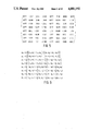
- FIG. 5 shows an 8 ⁇ 8 DCT matrix
- FIG. 6 shows the result of the product of eight input words with the 8 ⁇ 8 DCT matrix shown in FIG. 5,
- FIG. 7 shows a modification of the equations shown in FIG. 6,
- FIG. 8 shows a diagram of the DCT algorithm of FIG. 7,
- FIG. 9 shows a diagram of the inverse DCT algorithm
- FIGS. 10(I) and 10(II) show a possible time diagram to explain the transformer shown in FIG. 4 which is programmed for performing the DCT algorithm shown in the diagram of FIG. 8, and
- FIGS. 11(I) and 11(II) show a time diagram to explain the transformer shown in FIG. 4 which is programmed for performing the inverse DCT algorithm shown in the diagram of FIG. 9.
- FIG. 1 shows a diagrammatically a video recorder. It comprises an encoding station 1 and a decoding station 2.
- the encoding station 1 has an input 10 for the reception of a picture signal s(t) which is supplied by a picture signal source 3; for example a video camera.
- the output 11 of this encoding station is connected to a write head 4 by means of which the processed analog picture signals s(t) can be registered on a magnetic tape 5.
- a read head 6 is connected to the input 20 of the decoding station for converting the information present on the magnetic tape 5 into electrical signals.
- the decoding station 2 supplies an analog picture signal s'(t) from its output 21, which signal can be applied to a monitor 7.
- the analog picture signal s(t) is sampled in a sampling circuit 12 at a suitably chosen sampling frequency of approximately 10 MHz so that a series of picture signal samples, also referred to as pixels, is obtained.
- Each pixel is encoded in an analog-to-digital converter 13 into, for example, an 8-bit PCM word s(n).
- these pixels are applied to a transform device 14(1) for performing a forward two-dimensional linear transform.
- this transform device 14(1) will be further described, it divides each television picture into sub-pictures of N ⁇ N pixels x i ,k each and transforms each sub-picture into an array of N ⁇ N weighting factors or coefficients y i ,k.
- i,k 0, 1, 2, . . . N-1.
- These weighting factors are subsequently applied to an encoding circuit 15, for example a so-called scene adaptive encoder many examples of which have been described in literature.
- each array of N ⁇ N coefficients into an auxiliary array of N ⁇ N quantised coefficients which differs from the original array in that the value of zero is allocated to the least significant coefficients. Subsequently the coefficients different from zero are coded with more or fewer bits in dependence upon their significance.
- a series of transmission words c(j) of variable length occurring serially and associated with a given array is produced at the output of this encoding circuit 15.
- the bits of these transmission words are applied via a digital channel modulator circuit 16 to the write head 4 and are registered on the magnetic tape.
- the signal supplied by the read head 6 is converted in a demodulator circuit 26 into transmission words c'(j) which correspond to the transmission words c(j) received in the encoding station by the modulator circuit 16.
- These transmission words c'(j) are applied to a decoding circuit 25 which converts each series of transmission words by addition of transmission words of the value zero into an array Y' of N ⁇ N coefficients y' i ,k which corresponds to the auxiliary array produced in the encoding circuit.
- This array Y' thus obtained is subsequently applied to a transform device 14(2) which is adapted to perform an inverse linear transform but whose structure is the same as that of the transform device 14(1).
- This transform device 14(2) converts the array Y' into an array X' of N ⁇ N pixels x' i ,k.
- This transform device supplies the series of picture signal samples s'(n) by placing the pixels of different arrays X' one after the other. These picture signal samples s'(n) are subsequently applied to a series arrangement of a digital-to-analog converter 23 and a low-pass filter 27 by which the analog picture signal s'(t) is obtained which can be displayed on the monitor 7 and which corresponds to the picture signal s(t) supplied by the signal source 3.
- the picture signal source 3 supplies a picture reset pulse FRS each time at the end of each full picture, which pulse can be used for different purposes.
- FIG. 2A shows the general structure of the transform device 14 (.). It has a terminal 14.01 at which the pixels s(n) occur and a terminal 14.02 at which the coefficients y i ,k occur. In conformity with the foregoing, it will be assumed that these are the coefficients of the coefficient array Y T . Furthermore two one-dimensional transformers 14.04(1) and 14.04(2) are provided and the transform matrix A is associated with each of them.
- the transoformer 14.04(1) is connected via two parallel-arranged picture memories 14.03(.) and terminal 14.04. Both transformers are mutually coupled by means of two parallel-arranged array memories 14.05(.) and transformer 14.04(2) is connected to terminal 14.02 by means of a coefficient register 14.06.
- the memories 14.03(.) are each provided with addressable memory locations and are controlled by write-read commands WR1 and WR2 in such a manner that information is written in one of them while simultaneously information present in the other memory is read.
- the address AD1, AD2 applied to the relevant memory determines at which memory location information is stored or which information is read.
- the memories 14.05(.) are controlled in a corresponding manner by the read-write commands WR3 and WR4 and the addresses AD3 and AD4.
- the memories 14.03(.) and 14.05(.) are controlled in a corresponding manner, that is to say, information is written in one memory and read in the other, these memories are distinguished by their capacity. More particularly the memory 14.03(.) comprises at least as many rows of memory locations as there are visible lines in a TV picture and each row comprises as many memory locations as there are visible pixels in a TV line. Such a memory is shown diagrammatically in FIG. 3. In this Figure the reference LN denotes the row number of the memory and PN denotes the location number on the line (also referred to as the column number).
- the array memory 14.05(.) has a capacity which is at least equal to the dimensions of the transform matrix A.
- this picture memory comprises the pixels denoted by dots in FIG. 3.
- each picture is split up into a plurality of sub-pictures each of N ⁇ N pixels.
- N 8 in FIG. 3.
- the contents of such a sub-memory are considered to be an array of pixels and will be denoted by X.
- the pixels of such an array are read successively and row by row and are applied to the first one-dimensional transformer 14.04(1).
- This transformer thus receives the transposed version P T of the product array P, multiplies it also by the transform matrix A and thus supplies successively and row by row the product words evaluated as coefficients of the N ⁇ N coefficient matrix Y T . These coefficients are temporarily stored in the coefficient register 14.06.
- the control circuit shown in FIG. 2B receives clock pulses occurring at a rate f s from a clock pulse generator 8. It is to be noted that these clock pulses are also applied as sampling pulses to the sampling circuit 12 (see FIG. 1). In this control circuit they are applied to a pixel counter 14.10 whose counting position ranges from zero to a number which is equal to the number of pixels constituting a full picture. This counter is reset at the commencement of each new picture by picture reset pulses FRS which are supplied by the video signal source 3 (FIG. 1). The counting positions of this pixel counter are applied as addresses to two memories 14.11(1) each in the form of a ROM.
- the ROM 14.11(1) supplies the addresses for the picture memories 14.03(.) in the sequence in which pixels must be read (read addresses), whilst the ROM 14.11(2) supplies the addresses for the picture memories 14.03(.) in the sequence in which pixels must be written into the picture memory (write addresses).
- the addresses supplied by these ROMs 14.11(.) are applied via AND gate circuits 14.12(.) and OR gate circuits 14.13(.) to the picture memories 14.03(.).
- the picture reset pulses FRS are also applied to a T-flip-flop 14.14. Its Q output supplies the write-read command WR1 and its Q output supplies the write-read command WR2. These commands are applied in the manner shown to the AND gate circuits 14.12(.).
- the counting positions of pixel counter 14.10 are also applied to two further memories 14.15(.) which are both in the form of ROMs.
- the ROM 14.15(1) comprises the N ⁇ N read addresses for the array memories and the ROM 14.15(2) comprises the N ⁇ N write addresses. These addresses supplied by the two ROMs 14,15(.) are applied via AND gate circuits 14.16(.) and OR gate circuits 14.17(.) to the array memories.
- the read addresses of ROM 14.15(1) are also applied to a comparison circuit 14.18 which applies a control pulse to the T input of a T-flip-flop 14.19 whenever a predetermined read address occurs.
- the Q output of this T-flip-flop supplies the write-read command WR3 and its Q output supplies the write-read command WR4.
- the coefficients of the N ⁇ N coefficient array Y T presented to terminal 14.02 are applied successively and row by row to the transformer 14.04(2) via the coefficient register 14.06.
- These product words are stored in the array memory 14.05(.). Subsequently the product words are read successively and column by column and are applied to the transformer 14.04(1).
- This transformer thus receives the transposed version P' T of the product array P, multiplies this array also by the transform matrix A and thus supplies successively and row by row the product words evaluated as pixels of a sub-picture of N ⁇ N pixels.
- Such a sub-picture is again stored in a suitable sub-memory of a picture memory 14.03(.). After all sub-memories of the picture memory have been provided with a new sub-picture, the pixels in this picture memory are read successively and row by row so that the series of pixels s(n) is obtained.
- an element applied to the transformer 14.04(.) (such as a pixel, a product word, a coefficient) will hereinafter be referred to as an input word and the element which it supplies (such as a product word, a coefficient, a pixel) will be referred to as a product word.
- the transform matrix A which is associated with this transformer 14.04(.) is an N ⁇ N matrix so that in this transformer each of a series of N input words is converted into a series of N product words.
- the input words of such a series will be denoted by d 0 , d 1 , d 2 , . . . d N-1 and the product words of the series obtained will be denoted by p 0 , p 1 , . . . . p N-1 , respectively.
- each of the one-dimensional transformer 14.04(.) has an input bus connection 14.20 and an output bus connection 14.21.
- a main input connection bus 14.22 across which the input words d k are transported is connected to the input bus connection. It is to be noted that the bits of the different words are assumed to be available in parallel so that a bus has at least as many parallel lines as the word which is transported thereacross has bits.
- the transformer also comprises a first, second and third data connection buses 14.23, 14.24, 14.25, respectively, first, second and third column buses 14.26, 14.27, 14.28 and a main output connection bus 14.29. The latter bus is connected to the output bus connection 14.21.
- the first column bus 14.26 is selectively connectable at any instant to not more than one of a first set of connection buses 14.22, 14.23, 14.24 by means of a first set of switches SW1, SW2, SW3.
- the second column bus 14.27 is selectively connectable at any instant to not more than one bus of a second set of connection buses 14.22, 14.23, 14.25 by means of a second set of switches SW4, SW5, SW6.
- the third column bus 14.28 is selectively connectable at any instant to not more than one bus of a third set of connection buses 14.22, 14.24, 14.25 by means of a third set of switches SW7, SW8, SW9.
- the main output connection bus is selectively connectable at any instant to not more than one of the data connection buses 14.23, 14.24, 14.25 by means of a fourth set of switches SW10, SW11, SW12.
- the three switches SW1, SW2, SW3 of the first set are controlled by the respective first control signals S1, S2, S3.
- the three switches SW4, SW5, SW6 of the second set are controlled by the respective second control signals S4, S5, S6.
- the three switches SW7, SW8, SW9 of the third set are controlled by the respective third control signals S7, S8, S9.
- the three switches SW10, SW11, SW12 of the fourth set are controlled by the respective control signals S10, S11, S12.
- the logic state of the control signal controlling a given switch determines whether this switch has established a connection at a given instant.
- the one-dimensional transformer further comprises a first combination circuit 14.30, a second combination circuit 14.31 and a multiplier circuit 14.32.
- the first combination circuit 14.30 has an input bus connection 14.33 which is connected to the first column bus 14.26 and it has an output bus connection 14.34 which is connected to the third connection bus 14.25.
- the second combination circuit 14.31 has an input bus connection 14.35 which is connected to the third column bus 14.28. Furthermore it has an output bus connection 14.36 which is connected to the first connection bus 14.23.
- the multiplier circuit 14.32 has two input bus connections 14.37(1) and 14.37(2). The first connection is connected to the second column bus 14.27. It is also provided with the output bus connection 14.38 which is connected to the second connection bus 14.24.
- the combination circuits 14.30 and 14.31 each comprise two register banks R1, R2 and R3, R4, respectively of, for example, 12 registers of 12 bits. More particularly they are each formed by a so-called multiport register bank. Embodiments of these register banks are widely known. Some more interesting embodiments have recently been published in References 3 and 4. The characteristic feature of such register banks is that a given register can be written into while simultaneously the contents of another register can be read. An address determines which register is written into or from which register the contents are read. In the Figure the addresses for the registers banks R1, . . . , R4 are denoted by AD5, AD6, AD7, AD8, respectively.
- Each of these register banks has an input which is connected to the input bus connection 14.33 and 14.35, respectively and an output which is connected to the output bus connection 14.34 and 14.36, respectively, of the relevant combination circuit. They may also be provided with further outputs 14.39, 14.40 and 14.41, 14.42 which are connected to inputs of an adding/subtracting unit A/S(.). These units receive via a further input an adding/subtracting command +/-(.) and supply sum or difference words which are optionally stored in a register of register bank R1 or R2 or in a register of register bank R3 or R4, respectively.
- the multiplier circuit 14.32 has in input register bank M1 and an output register bank M2 each with, for example, not more than four 12-bit registers addressable by addresses AD9 and AD10, respectively.
- An input of register bank M1 is connected to the input bus connection 14.37(1) and an output is connected to a first input of a multiplier 14.43.
- This multiplier also receives a cyclic series of multiplication factors which are applied to the input bus connection 14.37(2) and supplies product words at an output. These are stored in a register of the output register bank M2 whose output is connected to the output bus connection 14.38.
- the said multiplication factors receives by the multiplier 14.43 are supplied by a memory unit 14.44 and are applied via a multiplication factor output bus 14.44(1) to the input bus connection 14.37(2) of the multiplier circuit.
- This memory unit 14.44 has memory locations which are addressable by means of an address AD11.
- this one-dimensional transformer is provided with a memory 14.45 with addressable memory locations (for example a ROM).
- Each memory location comprises a plurality of bits which define the state of all transformer circuits to be controlled at any moment, i.e. the state of the switches SW, the different addresses, and so forth. It appears in practice that approximately 70 bits per instant may suffice and that 16 of these 70 bits memory locations are required both for performing a forward Discrete Cosine Transform and, for performing an inverse Discrete Cosine Transform. These bits are applied by means of a bus 14.46 of approximately 70 parallel lines to the different elements of the circuit.
- This memory is in turn addressed by the counting positions of a counter circuit 14.47 (a modulo-16-counter in the case of a DCT) which receives counting pulses from a frequency multiplier 14.48. The latter multiplies the frequency of the clock pulses applied thereto by a factor of 2. The said clock pulses occur at the sampling frequency f s and are supplied, for example by the clock pulse generator 8 shown in FIG. 2B.
- a counter circuit 14.47 a modulo-16-counter in the case of a DCT
- the latter multiplies the frequency of the clock pulses applied thereto by a factor of 2.
- the said clock pulses occur at the sampling frequency f s and are supplied, for example by the clock pulse generator 8 shown in FIG. 2B.
- the transform matrix A is the discrete cosine transform matrix and that the one-dimensional transforms (forward and inverse) are performed in accordance with the algorithms which will be explained in the following section.
- the elements a i ,k of the N ⁇ N discrete cosine transform matrix A are defined as follows: ##EQU1## with D being a scaling constant which is equal to 2/N if the matrix is used for performing a forward transform and which is equal to 1 if it is used for performing an inverse transform.
- the absolute value of each element a i ,k of the discrete cosine transform matrix can be equated to such a transform element if these elements are defined as follows:
- This diagram comprises a number of combination points which are marked by dots and at which the data words applied to such a dot are added together or subtracted from one another. In the latter case the digit -1 is indicated next to a branch terminating at said combination point. Futhermore a plurality of nodes is present from which a given data word is applied via different branches to different combination points.
- the first-order sum words u 1 ,r and the first-order difference words v 1 ,r are obtained by performing adding and subtracting operations.
- the first-order sum words u 1 ,r are converted in a second iteration step into second-order sum words u 2 ,r and second-order difference words v 2 ,r.
- Q represents the largest integer which is smaller than or equal to -1+ 2 log N.
- the difference words obtained in the q-th iteration step are subjected to a plurality of further iteration steps in which a plurality of auxiliary sum words is obtained from the difference words v q ,r.
- the auxiliary sum word obtained in the j-th iteration step starting from the words v q ,r is generally denoted by w q ,j,m in which m is the ordinal number of the auxiliary sum word in the j-th iteration step.
- w q ,j,m In conformity with the foregoing w q ,j,m will be referred to as a j-th order auxiliary sum word.
- n inverse transform is the transform which is described in the diagram of FIG. 9
- Comparison of the diagram of FIG. 8 with that of FIG. 9 shows that the latter follows from the first by transposing the first diagram of FIG. 8 (see Reference 5). This means that the signal direction is inverted therein, the combination points are replaced by nodes and the nodes are replaced by combination points.
- FIG. 10 The operation of the one-dimensional transformer for performing the forward DCT algorithm defined in the previous section is shown diagrammatically in the time diagram of FIG. 10 which is self-evident.
- column T indicates the counting positions of the modulo-16-counter.
- the columns denoted by R1, R2, R3, R4, M1, M2 relate to the contents of the different register banks. More particularly the columns r 0 , r 1 , . . ., and m o , m 1 , . . . , indicate the contents of the relevant registers of these register banks.
- the columns denoted by A/S(1) and A/S(2) indicate which quantities at this counting position T of counter 14.47 are added together or are subtracted from one another in the adding/subtracting units A/S(1) and A/S(2), respectively.
- the column denoted by M2 indicates the sub-product supplied by the multiplier 14.43 and stored in the register m 1 , m 2 , m 3 or m 4 with the same designation as in FIG. 8.
- Finally the column denoted by OUT indicates the product words p k occurring at the output 14.21.
- u 1 ,2 is stored in register r 2 of R2, z 11 is stored in register r 0 of R3, z 12 is stored in register m 0 of M2. Furthermore v 1 ,2 is stored in register m 0 of M1 and multiplied by C 7 16 +C 1 16 resulting in the product z 5 . Furthermore d 6 is stored in register r 0 of R2 and d 6 is subtracted from d 1 so that v 1 ,1 is obtained. Corresponding operations are performed at the further counting positions of counter 14.47.
- FIG. 10 accurately describes the data flow through the transformer, the contents of the memory 14.45 is fully defined thereby.
- FIG. 11 The operation of the one-dimensional transformer for performing the IDCT algorithm shown in FIG. 9 is indicated diagrammatically in the time diagram of FIG. 11.
- the different columns have the same significance as those in FIG. 10.
- the data flow indicated in this FIG. 11 uniformly defines the contents of the memory 14.45.
Landscapes
- Physics & Mathematics (AREA)
- Engineering & Computer Science (AREA)
- General Physics & Mathematics (AREA)
- Mathematical Physics (AREA)
- Pure & Applied Mathematics (AREA)
- Theoretical Computer Science (AREA)
- Mathematical Optimization (AREA)
- Mathematical Analysis (AREA)
- Computational Mathematics (AREA)
- Data Mining & Analysis (AREA)
- Algebra (AREA)
- Databases & Information Systems (AREA)
- Software Systems (AREA)
- General Engineering & Computer Science (AREA)
- Discrete Mathematics (AREA)
- Computing Systems (AREA)
- Compression Or Coding Systems Of Tv Signals (AREA)
- Complex Calculations (AREA)
- Signal Processing For Digital Recording And Reproducing (AREA)
Applications Claiming Priority (2)
| Application Number | Priority Date | Filing Date | Title |
|---|---|---|---|
| NL8700845A NL8700845A (nl) | 1987-04-10 | 1987-04-10 | Een-dimensionale lineaire beeldtransformator. |
| NL8700845 | 1987-04-10 |
Publications (1)
| Publication Number | Publication Date |
|---|---|
| US4881192A true US4881192A (en) | 1989-11-14 |
Family
ID=19849839
Family Applications (1)
| Application Number | Title | Priority Date | Filing Date |
|---|---|---|---|
| US07/178,952 Expired - Lifetime US4881192A (en) | 1987-04-10 | 1988-04-07 | One-dimensional linear picture transformer |
Country Status (6)
| Country | Link |
|---|---|
| US (1) | US4881192A (ja) |
| EP (1) | EP0286184B1 (ja) |
| JP (1) | JP2630801B2 (ja) |
| KR (1) | KR970004534B1 (ja) |
| DE (1) | DE3866149D1 (ja) |
| NL (1) | NL8700845A (ja) |
Cited By (7)
| Publication number | Priority date | Publication date | Assignee | Title |
|---|---|---|---|---|
| US5089982A (en) * | 1990-05-24 | 1992-02-18 | Grumman Aerospace Corporation | Two dimensional fast Fourier transform converter |
| US5339265A (en) * | 1992-08-31 | 1994-08-16 | University Of Maryland At College Park | Optimal unified architectures for the real-time computation of time-recursive discrete sinusoidal transforms |
| US5781239A (en) * | 1996-06-20 | 1998-07-14 | Lsi Logic Corporation | System and method for performing an optimized inverse discrete cosine transform with improved efficiency |
| US5793658A (en) * | 1996-01-17 | 1998-08-11 | Digital Equipment Coporation | Method and apparatus for viedo compression and decompression using high speed discrete cosine transform |
| US6072935A (en) * | 1991-04-18 | 2000-06-06 | U.S. Philips Corporation | System and method for improving video recorder performance in a search mode |
| US6125438A (en) * | 1997-04-21 | 2000-09-26 | Matsushita Electrical Industrial Co., Ltd. | Data processor |
| US7142720B1 (en) * | 1990-07-31 | 2006-11-28 | Fujitsu Limited | Image data processing method and apparatus |
Families Citing this family (9)
| Publication number | Priority date | Publication date | Assignee | Title |
|---|---|---|---|---|
| US5008848A (en) * | 1989-05-30 | 1991-04-16 | North American Philips Corporation | Circuit for performing S-transform |
| US5450557A (en) * | 1989-11-07 | 1995-09-12 | Loral Aerospace Corp. | Single-chip self-configurable parallel processor |
| JPH04102170A (ja) * | 1990-08-21 | 1992-04-03 | Fujitsu Ltd | マトリクス演算装置,マトリクスク演算方法及びその応用装置 |
| US5870497A (en) * | 1991-03-15 | 1999-02-09 | C-Cube Microsystems | Decoder for compressed video signals |
| EP0509594B1 (en) * | 1991-04-18 | 1997-10-22 | Koninklijke Philips Electronics N.V. | System and method for improving video recorder performance in a search mode |
| US5444490A (en) * | 1992-07-07 | 1995-08-22 | U.S. Philips Corporation | Television system for transmitting pictures in a digital form |
| DE69423389T2 (de) * | 1993-06-07 | 2000-09-21 | Koninkl Philips Electronics Nv | Vorrichtung zur Übertragung oder Aufzeichnung von digitalen Fernsehbildern, und Vorrichtung zum Empfang derselben |
| JP2000507006A (ja) * | 1997-01-10 | 2000-06-06 | コーニンクレッカ フィリップス エレクトロニクス エヌ ヴィ | 画像投射装置の照射システム |
| AU752024B2 (en) | 2000-04-14 | 2002-09-05 | Kabushiki Kaisha Toshiba | Method and equipment for assessing the life of members put under high in-service temperature environment for long period |
Citations (5)
| Publication number | Priority date | Publication date | Assignee | Title |
|---|---|---|---|---|
| US4138730A (en) * | 1977-11-07 | 1979-02-06 | Communications Satellite Corporation | High speed FFT processor |
| US4449194A (en) * | 1981-09-25 | 1984-05-15 | Motorola Inc. | Multiple point, discrete cosine processor |
| US4675836A (en) * | 1984-03-09 | 1987-06-23 | Compagnie Industrielle Des Telecommunications Cit-Alcatel | Discrete cosine transform calculation processor |
| US4787055A (en) * | 1984-07-20 | 1988-11-22 | Thomson-Csf | Circuit for calculating the discrete Fourier transform |
| US4791598A (en) * | 1987-03-24 | 1988-12-13 | Bell Communications Research, Inc. | Two-dimensional discrete cosine transform processor |
Family Cites Families (1)
| Publication number | Priority date | Publication date | Assignee | Title |
|---|---|---|---|---|
| NL8004521A (nl) * | 1980-08-08 | 1982-03-01 | Philips Nv | Werkwijze voor het digitaliseren van een kleuren-videosignaal. |
-
1987
- 1987-04-10 NL NL8700845A patent/NL8700845A/nl not_active Application Discontinuation
-
1988
- 1988-04-04 JP JP63082871A patent/JP2630801B2/ja not_active Expired - Lifetime
- 1988-04-06 DE DE8888200640T patent/DE3866149D1/de not_active Expired - Lifetime
- 1988-04-06 EP EP88200640A patent/EP0286184B1/en not_active Expired - Lifetime
- 1988-04-07 US US07/178,952 patent/US4881192A/en not_active Expired - Lifetime
- 1988-04-09 KR KR88004035A patent/KR970004534B1/ko not_active IP Right Cessation
Patent Citations (5)
| Publication number | Priority date | Publication date | Assignee | Title |
|---|---|---|---|---|
| US4138730A (en) * | 1977-11-07 | 1979-02-06 | Communications Satellite Corporation | High speed FFT processor |
| US4449194A (en) * | 1981-09-25 | 1984-05-15 | Motorola Inc. | Multiple point, discrete cosine processor |
| US4675836A (en) * | 1984-03-09 | 1987-06-23 | Compagnie Industrielle Des Telecommunications Cit-Alcatel | Discrete cosine transform calculation processor |
| US4787055A (en) * | 1984-07-20 | 1988-11-22 | Thomson-Csf | Circuit for calculating the discrete Fourier transform |
| US4791598A (en) * | 1987-03-24 | 1988-12-13 | Bell Communications Research, Inc. | Two-dimensional discrete cosine transform processor |
Cited By (8)
| Publication number | Priority date | Publication date | Assignee | Title |
|---|---|---|---|---|
| US5089982A (en) * | 1990-05-24 | 1992-02-18 | Grumman Aerospace Corporation | Two dimensional fast Fourier transform converter |
| US7142720B1 (en) * | 1990-07-31 | 2006-11-28 | Fujitsu Limited | Image data processing method and apparatus |
| US6072935A (en) * | 1991-04-18 | 2000-06-06 | U.S. Philips Corporation | System and method for improving video recorder performance in a search mode |
| US6167191A (en) * | 1991-04-18 | 2000-12-26 | U.S. Philips Corporation | System and method for improving video recorder performance in a search mode |
| US5339265A (en) * | 1992-08-31 | 1994-08-16 | University Of Maryland At College Park | Optimal unified architectures for the real-time computation of time-recursive discrete sinusoidal transforms |
| US5793658A (en) * | 1996-01-17 | 1998-08-11 | Digital Equipment Coporation | Method and apparatus for viedo compression and decompression using high speed discrete cosine transform |
| US5781239A (en) * | 1996-06-20 | 1998-07-14 | Lsi Logic Corporation | System and method for performing an optimized inverse discrete cosine transform with improved efficiency |
| US6125438A (en) * | 1997-04-21 | 2000-09-26 | Matsushita Electrical Industrial Co., Ltd. | Data processor |
Also Published As
| Publication number | Publication date |
|---|---|
| KR970004534B1 (en) | 1997-03-28 |
| NL8700845A (nl) | 1988-11-01 |
| KR880013401A (ko) | 1988-11-30 |
| JPS6427378A (en) | 1989-01-30 |
| JP2630801B2 (ja) | 1997-07-16 |
| DE3866149D1 (de) | 1991-12-19 |
| EP0286184A1 (en) | 1988-10-12 |
| EP0286184B1 (en) | 1991-11-13 |
Similar Documents
| Publication | Publication Date | Title |
|---|---|---|
| US4831440A (en) | Television transmission system using transform coding | |
| US4881192A (en) | One-dimensional linear picture transformer | |
| EP0013069B1 (en) | A data processor and method of processing video information | |
| US5999957A (en) | Lossless transform coding system for digital signals | |
| KR100246878B1 (ko) | 역이산 코사인변환 프로세서, 이산 코사인 변환계수의 매트릭스를 역변환하기 위한 방법 및 그 장치 | |
| US5168375A (en) | Image reconstruction by use of discrete cosine and related transforms | |
| CA1290854C (en) | Two-dimensional discrete cosine transform processor | |
| US4912668A (en) | Mono-dimensional reverse cosine transform computing device | |
| US5638533A (en) | Method and apparatus for providing data to a parallel processing array | |
| US5321797A (en) | Apparatus and method for performing coordinate transformation employing stored values and interpolation | |
| US5331585A (en) | Orthogonal transformation processor for compressing information | |
| US6421695B1 (en) | Apparatus for implementing inverse discrete cosine transform in digital image processing system | |
| US4837724A (en) | Discrete cosine transform arrangement | |
| JPH01226274A (ja) | 画像圧縮処理のための方法及びシステム | |
| JP3278756B2 (ja) | 画像処理方法及び装置 | |
| WO1997022938A1 (en) | Manipulating video and audio signals using a processor which supports simd instructions | |
| US5291429A (en) | Circuit for matrix calculation of discrete cosine transformation | |
| EP0566184A2 (en) | Picture transformer and television system with a transmitter and a receiver comprising a picture transformer | |
| GB2061660A (en) | Modifying the contrast of an image | |
| US4860097A (en) | Transformation circuit | |
| US5359549A (en) | Orthogonal transformation processor for compressing information | |
| US4953020A (en) | Television transmission system with differential encoding of transform coefficients | |
| US4953018A (en) | Television Transmission system using transmission of basic picture weighting factors | |
| EP0511606A2 (en) | Parallel interpolator for high speed digital image enlargement | |
| AU666442B1 (en) | Image processing apparatus and method therefor |
Legal Events
| Date | Code | Title | Description |
|---|---|---|---|
| AS | Assignment |
Owner name: U.S. PHILIPS CORPORATION, 100 EAST 42ND STREET, NE Free format text: ASSIGNMENT OF ASSIGNORS INTEREST.;ASSIGNORS:WOUDSMA, ROBERTO;CHONG, DAVID C. H.;MC SWEENEY, BRIAN T.;REEL/FRAME:004978/0122;SIGNING DATES FROM 19880705 TO 19881104 Owner name: U.S. PHILIPS CORPORATION, A CORP. OF DE, NEW YORK Free format text: ASSIGNMENT OF ASSIGNORS INTEREST;ASSIGNORS:WOUDSMA, ROBERTO;CHONG, DAVID C. H.;MC SWEENEY, BRIAN T.;SIGNING DATES FROM 19880705 TO 19881104;REEL/FRAME:004978/0122 |
|
| AS | Assignment |
Owner name: U.S. PHILIPS CORPORATION, 100 EAST 42ND STREET, NE Free format text: ASSIGNMENT OF ASSIGNORS INTEREST.;ASSIGNORS:BORGERS, STEPHANUS M. C.;HABRAKEN, EGIDIUS A. P.;REEL/FRAME:004983/0512 Effective date: 19880708 Owner name: U.S. PHILIPS CORPORATION, A CORP. OF DE., NEW YO Free format text: ASSIGNMENT OF ASSIGNORS INTEREST;ASSIGNORS:BORGERS, STEPHANUS M. C.;HABRAKEN, EGIDIUS A. P.;REEL/FRAME:004983/0512 Effective date: 19880708 |
|
| STCF | Information on status: patent grant |
Free format text: PATENTED CASE |
|
| FEPP | Fee payment procedure |
Free format text: PAYOR NUMBER ASSIGNED (ORIGINAL EVENT CODE: ASPN); ENTITY STATUS OF PATENT OWNER: LARGE ENTITY |
|
| FPAY | Fee payment |
Year of fee payment: 4 |
|
| FPAY | Fee payment |
Year of fee payment: 8 |
|
| FPAY | Fee payment |
Year of fee payment: 12 |