US4725762A - Circuit supplied with direct voltage for generating voltages and/or currents with different curve form and/or different frequency and/or different polarity with at least one load - Google Patents
Circuit supplied with direct voltage for generating voltages and/or currents with different curve form and/or different frequency and/or different polarity with at least one load Download PDFInfo
- Publication number
- US4725762A US4725762A US06/928,285 US92828586A US4725762A US 4725762 A US4725762 A US 4725762A US 92828586 A US92828586 A US 92828586A US 4725762 A US4725762 A US 4725762A
- Authority
- US
- United States
- Prior art keywords
- gas discharge
- discharge lamp
- semiconductor switches
- switch
- series
- Prior art date
- Legal status (The legal status is an assumption and is not a legal conclusion. Google has not performed a legal analysis and makes no representation as to the accuracy of the status listed.)
- Expired - Fee Related
Links
Images

Classifications
-
- H—ELECTRICITY
- H02—GENERATION; CONVERSION OR DISTRIBUTION OF ELECTRIC POWER
- H02M—APPARATUS FOR CONVERSION BETWEEN AC AND AC, BETWEEN AC AND DC, OR BETWEEN DC AND DC, AND FOR USE WITH MAINS OR SIMILAR POWER SUPPLY SYSTEMS; CONVERSION OF DC OR AC INPUT POWER INTO SURGE OUTPUT POWER; CONTROL OR REGULATION THEREOF
- H02M7/00—Conversion of AC power input into DC power output; Conversion of DC power input into AC power output
- H02M7/42—Conversion of DC power input into AC power output without possibility of reversal
- H02M7/44—Conversion of DC power input into AC power output without possibility of reversal by static converters
- H02M7/48—Conversion of DC power input into AC power output without possibility of reversal by static converters using discharge tubes with control electrode or semiconductor devices with control electrode
- H02M7/53—Conversion of DC power input into AC power output without possibility of reversal by static converters using discharge tubes with control electrode or semiconductor devices with control electrode using devices of a triode or transistor type requiring continuous application of a control signal
- H02M7/537—Conversion of DC power input into AC power output without possibility of reversal by static converters using discharge tubes with control electrode or semiconductor devices with control electrode using devices of a triode or transistor type requiring continuous application of a control signal using semiconductor devices only, e.g. single switched pulse inverters
- H02M7/5387—Conversion of DC power input into AC power output without possibility of reversal by static converters using discharge tubes with control electrode or semiconductor devices with control electrode using devices of a triode or transistor type requiring continuous application of a control signal using semiconductor devices only, e.g. single switched pulse inverters in a bridge configuration
Definitions
- the invention is directed to a circuit supplied with direct voltage for generating voltages and/or currents with different curve forms and/or different frequencies and/or different polarities, with at least one load.
- An object of the invention is to develop a circuit proceeding from a direct voltage supply, with which the solution of the task is possible.
- the invention is characterized by a choke coil arranged in series with this load and at least two controlled semiconductor switches, which each lie in a series circuit as far as the load and the choke coil are concerned.
- these two switches lie in different current paths and these current paths are connected at differing potentials of the supply voltage, wherein, in actual operation, one switch is held open while the other switch is opened and closed in alternating sequence, and, after the termination of an adjustable or selectable time period the switch which has hitherto been actuated in alternating sequence (clock pulse frequency) is kept open, while the hitherto held open switch is, in alternating sequence, opened and closed, this alternating sequence of switch actuation (polarity reversal frequency) being continuously repeated.
- clock pulse frequency the switch which has hitherto been actuated in alternating sequence
- this alternating sequence of switch actuation polarity reversal frequency
- a particularly simple circuit of this type is characterized in accordance with a feature of the invention by the current path containing the load and the choke in series arrangement being connected at an average value of the supply voltage.
- An additional circuit of this type also suitable for low outputs and particularly low frequencies is characterized, in accordance with an additional feature of the invention, by the current path containing the load and the choke in series arrangement being connected at different potentials of the supply voltage through at least two condensers, which each lie in series, as far as the load and the choke coil are concerned, but which, however, lie in different current paths, wherein the condensers are connected at the same potentials of the supply voltage as the controlled semiconductor switches.
- Another circuit which satisfies all requirements as far as the output and variation possibilities are concerned, is characterized, in accordance with an additional feature of the invention, in that the current path containing the load and the choke in series arrangement is connected at differing potentials of the supply voltage through two additional controllable semiconductor switches, which each lie in series arrangement with respect to the load and the choke coil, but which, however, lie in different current paths, wherein these additional semiconductor switches are opened or closed in the period of the polarity reversal frequency of the other semiconductor switches and thus form, respectively, a closed current circuit in connection with the load and the choke coil, in which the direction of the current flow changes in accordance with the polarity reversal frequency.
- a condenser is connected in parallel with a load, then the current and/or the voltage is smoothed out; a similar effect is achieved if a condenser is connected between the choke and the load whose other electrode is connected with the connection point for the supply of voltage which exhibits the lower voltage of the two connection points of this supply voltage.
- the magnitude of the ratio of the polarity reversal frequency to the clock pulse frequency or timing frequency determines the regulation quality of the circuit; the larger this ratio is, the smaller the choke can be made. It is therefore desirable to arrange this ratio at approximately 1:1000, or preferably even higher.
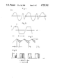
- FIG. 1, FIG. 2 and FIG. 3 show three different embodiments of the invention
- FIG. 4 and FIG. 5 show voltage- or current flow diagrams
- FIG. 6 shows a pulse diagram for the cycle control of the semiconductor switches
- FIG. 7 shows a detail from the current flow diagram according to FIG. 5 at a greatly magnified scale.
- FIG. 1 illustrates a first embodiment example of a circuit according to the invention.
- a battery B with a central tap and with the terminal voltage U serves here as a voltage source.
- the line branch 3, comprising a choke D and a load L in series is, on the one hand, connected to the central tap of the battery B, and, on the other hand, between two control semiconductor switches T 1 and T 2 , of which each is connected with one respective terminal of the battery B so that each semiconductor switch lies in a series circuit with the choke D and the load L.
- the control of the semiconductor switches T 1 and T 2 is additionally explained in detail in the following.
- the semiconductor switch T 1 is cyclically continuously opened and closed (clock pulse frequency) and during this time period, the other semiconductor switch T 2 is kept open.
- This continuous opening and closing of the one switch, while the other switch is open, is here and in what follows designated as clock pulse frequency.
- the switch T 1 is held open, wherein now the other switch T 2 is continuously opened and closed.
- These modes are actuated cyclically.
- This change in the actuation of the switches T 1 and T 2 is here and in the following designated as polarity reversal frequency. This process can now be repeated as often as desired.
- the one semiconductor switch T 1 While the one semiconductor switch T 1 is actuated cyclically, current flows in the one direction (arrow 4) through the load L. While the semiconductor switch T 2 is operated cyclically, the current flows in the opposite direction through the load L.
- the magnitude of the load current depends now, on the one hand, on the inductance of the choke and the clock pulse frequency of the switches T 1 and T 2 ; the time period of current flow in, respectively, one direction depends on the polarity reversal frequency.
- the clock pulse frequency as well as the polarity reversal frequency are controllable by different magnitudes, which will be additionally dealt with in the following.
- FIG. 2 An additional circuit with which, in particular, low frequency voltages or currents starting from a direct voltage can be obtained is shown in FIG. 2.
- the voltage U is applied to the terminals XY of the circuit, recovery diodes D 1 and D 2 are provided in parallel to the semiconductor switches T 1 and T 2 .
- One condenser C each is arranged in series with the load L and the choke D in different current circuits, so that the current path comprising the load and the choke in series is connected at different potentials of the supply voltage through the two condensers, which each are in series as far as the load and the choke are concerned, but, however, which lie in different current paths, wherein the condensers C are connected to the same potentials of the supply voltage U as the controlled semiconductor switches T 1 and T 2 .
- the controlled semiconductor switches T 1 and T 2 are actuated in the sense of the clock pulse frequency and the polarity reversal frequency mentioned above.
- the frequency of the voltage existing at the load L is herein dependent, among other things, on the capacity and the time constant of the condensers.
- FIG. 3 A circuit which can satisfy all the requirements, and which constitute a direct refinement of the previously explained circuits, is now shown in FIG. 3.
- This circuit supplied with constant voltage, is designed as a bridge circuit.
- a transistor T 1 to T 4 is arranged in each outer branch of this bridge voltage.
- Two of these transistors namely the transistors T 1 and T 2 which lie between the connecting points X and Y for the supply voltage U, comprises recovery diodes D 1 and D 2 arranged in parallel to said transistors.
- Diodes D 3 and R 4 are arranged in parallel with the other two transistors T 3 and T 4 , for purposes of protection.
- the bases B 1 to B 4 of the transistors T 1 to T 4 are, for instance, connected with integrated circuits, which, however, are not shown here.
- the load L is connected at the terminals A and E in the diagonal branch of the bridge circuit.
- inductive and capacitive resistances can be used as a load, but also such which exhibit a complex resistance behavior.
- the choke D is connected between the terminal A and the point of connection F between the two transistors T 1 and T 2 serving as semiconductor switches.
- a condenser C provided here in parallel to the load.
- Another condenser C may be provided instead of the condenser parallel with the load L, whose one electrode lies between the load L and the choke D and whose other electrode lies at the point of connection Y for the supply voltage U, which point of connection exhibits the lower potential. This is indicated in FIG. 3 with a broken line.
- the transistors T 1 and T 2 serving as semiconductor switches, are actuated in the sense of the clock pulse frequency and polarity reversal frequency described above. Contrary to that, the transistors T 3 and T 4 , serving as semiconductor switches, are correspondingly switched only in accordance with the polarity reversal frequency.
- FIG. 6 illustrates a pulse sequence with which the bases of the transistors T 1 and T 2 can be controlled.
- PD signifies the duration of the period;
- ED the duration of the duty cycle (pulse length) and
- TL the time interval between pulses.
- the ratio between the duty cycle ED and the periodic cycle PD is designated as the pulse duty factor.
- This pulse duty factor is adjustable and changeable with the integrated circuit not shown here but which has been mentioned by way of an example.
- the direct voltage U being applied to the terminals X, Y can either be drawn from a power supply source, it can however also be made available by a converter (alternating current/direct current converter).
- the transistors T 1 to T 4 serve as electronic switches and their bases are controlled by the magnitude of the operating current through pulse sequences according to FIG. 6. In the first phase of the operation the transistors T 1 and T 4 are closed and the transistors T 2 and T 3 , on the other hand, are held open. In addition to the transistor T 1 or its basis B 1 is herein controlled by the pulse sequence shown in FIG. 6.
- the transistor T 1 is closed and direct current flows from the terminal X through the transistor T 1 , the choke D and the lamp L through the transistor T 4 which is held closed during this operational phase, to the terminal Y.
- the transistor T 1 Prior to reaching the rated magnitude of the lamp operating current, that is--viewed timewise--at the end of the duty cycle ED of the control pulse, the transistor T 1 opens, the current flow from the power supply source is interrupted and the magnetic energy built up in the choke D by the current flow is now converted into electrical energy and supplies an opposing voltage, which maintains the current flow through the lamp L in the same direction up to the start of the duty cycle time of the next control pulse, meaning that during the interval TL between duty cycles, in the course of which, the energy stored in the choke is used up.
- the transistor T 1 is again switched on by the next following control pulse at the base B 1 of the transistor T 1 , the transistor T 1 being again closed and therein new energy and current is supplied from the power source to the circuit in the manner described, up to shortly before reaching the rated magnitude of the lamp operational current, whereupon the mentioned switch-over process is again initiated and performed.
- current always flows in the same direction through the lamp L.
- the control processes described are very short and occur in fractions of seconds.
- the transistor T 4 remains closed. In order to avoid the mentioned damaging deposits because of direct voltage operation of the gas discharge lamp, after a certain time, the polarity of the lamp L is changed.
- the polarity reversal frequency can, for instance, be derived and controlled from the power source frequency, if the direct voltage at the terminals XY of the circuit is obtained by an alternating current--direct current converter (not shown). Also, other control frequencies for the polarity reversal can be utilized with success.
- the duration of the period of the polarity reversal frequency is therein always greater than the duration of the period of the control pulses (clock pulse frequency).
- the diodes D 1 and D 2 connected in parallel with transistors T 1 and T 2 serve as recovery diodes which maintain the current flow when the transistors T 1 and T 2 open and close controlled by the pulses, then the diodes D 3 and D 4 in parallel with the transistor T 3 and T 4 fulfill a protective function.
- FIG. 5 The current flow through the gas discharge lamp L in accordance with the circuit in FIG. 3 and the type of operation described above is depicted schematically in FIG. 5. Viewed overall, we are dealing here with a trapezoid-shaped progression with changing plus or minus signs. The period P of the sequence depends on the polarity change frequency. If the current flow, shown in the illustration with a straight line, is, so to speak, represented in a magnified manner, then there results a line which is shown in FIG. 7 and which represents the segments G encircled in the FIG. 5, so to speak, at a larger scale.
- This line extends in a jagged manner, its rise or fall is determined by the resistance behavior of the choke D and the load L, its reversal points depending on the clock pulse frequency and its smoothness (shaded areas) is determined by the smoothing-out condensers C according to the circuit in FIG. 3.
- a voltage progression can, for instance, also be forced as it is illustrated in FIG. 4.
- the load current was utilized for controlling the clock pulse frequency for the semiconductor switches T 1 and T 4 , meaning the semiconductor switches T 1 and T 4 were cyclically opened, respectively, before the load current, had reached the lamp rated current and they were again switched back into the circuit as soon as the load current had somewhat diminished.
- the current values at which switching on or switching off occurred are designated in the illustration in FIG. 7 with I E or I A .
- the polarity reversal frequency (P--FIG. 5) was derived from the frequency of a conventional alternating current voltage supply network with 50 Hertz. A control by a magnitude not depending upon the circuit in this case the line frequency of an alternating current voltage supply network is designated as external excitation.
- the polarity reversal frequency can be controlled by the voltage rise at the condensers C (natural frequency).
- Other control possibilities for the cycling frequency result from the selection of the ratio of the switch on duration ED to the switch off duration TL or, however, through changing the pulse duration PD (pulse width modulation).
- Programmable processes are appropriately utilized for controlling the clock pulse frequency, with the help of which regulation curves and control curves of any desired shape can be obtained.
- an alternating current, motor which can be supplied with alternating current voltage changing as far as its frequency and magnitude is concerned, can be used in order to regulate rpm and torque of the motor within wide limits.
Landscapes
- Engineering & Computer Science (AREA)
- Power Engineering (AREA)
- Circuit Arrangements For Discharge Lamps (AREA)
- Inverter Devices (AREA)
- Electronic Switches (AREA)
Applications Claiming Priority (2)
| Application Number | Priority Date | Filing Date | Title |
|---|---|---|---|
| AT304/85A AT392384B (de) | 1985-02-04 | 1985-02-04 | Vorschaltgeraet zum betrieb von gasentladungslampen mit gleichstrom |
| AT304/85 | 1985-02-04 |
Publications (1)
| Publication Number | Publication Date |
|---|---|
| US4725762A true US4725762A (en) | 1988-02-16 |
Family
ID=3487005
Family Applications (1)
| Application Number | Title | Priority Date | Filing Date |
|---|---|---|---|
| US06/928,285 Expired - Fee Related US4725762A (en) | 1985-02-04 | 1986-01-30 | Circuit supplied with direct voltage for generating voltages and/or currents with different curve form and/or different frequency and/or different polarity with at least one load |
Country Status (7)
| Country | Link |
|---|---|
| US (1) | US4725762A (de) |
| EP (1) | EP0210242A1 (de) |
| AT (1) | AT392384B (de) |
| AU (1) | AU588282B2 (de) |
| ES (1) | ES8800564A1 (de) |
| WO (1) | WO1986004752A1 (de) |
| ZA (1) | ZA86799B (de) |
Cited By (20)
| Publication number | Priority date | Publication date | Assignee | Title |
|---|---|---|---|---|
| US4887007A (en) * | 1987-02-18 | 1989-12-12 | U.S. Philips Corporation | DC-AC converter for supplying a gas and/or vapour discharge lamp |
| US5479334A (en) * | 1993-01-29 | 1995-12-26 | Magnetek S.P.A. | Inverter for the supply of discharge lamps with heated electrodes, with resonant circuit |
| DE4436825A1 (de) * | 1994-06-28 | 1996-01-04 | Matsushita Electric Works Ltd | Vorrichtung zum Betreiben einer Hochdruck-Gasentladungslampe |
| DE19523750A1 (de) * | 1995-06-29 | 1997-01-02 | Thomson Brandt Gmbh | Wechselstromquelle |
| US6124682A (en) * | 1996-11-19 | 2000-09-26 | Micro Tech Limited | Lamp driver circuit using resonant circuit for starting lamp |
| US6316888B1 (en) * | 1999-05-12 | 2001-11-13 | Patent-Treuhand-Gesellschaft Fuer Elektrische Gluehlampen Mbh | Ballast for at least one gas discharge lamp and method for operating such a ballast |
| US6426597B2 (en) | 1998-09-18 | 2002-07-30 | Knobel Ag Lichttechnische Komponenten | Circuit arrangement for operating gas discharge lamps |
| US6469919B1 (en) | 1999-07-22 | 2002-10-22 | Eni Technology, Inc. | Power supplies having protection circuits |
| US20040052125A1 (en) * | 2002-09-12 | 2004-03-18 | Switched Reluctance Drives Limited | Circuit for use with switched reluctance machines |
| US6876158B2 (en) | 2000-10-16 | 2005-04-05 | Tridonicatco Gmbh & Co. Kg | Electronic ballast with full bridge circuit |
| WO2006064182A1 (en) * | 2004-12-17 | 2006-06-22 | Harvard Engineering Plc | Hid ballast |
| US20060158911A1 (en) * | 1999-07-22 | 2006-07-20 | Lincoln Daniel J | Class E amplifier with inductive clamp |
| US20060254365A1 (en) * | 2005-05-10 | 2006-11-16 | Hamel Michael J | Wireless vibrating strain gauge for smart civil structures |
| DE102005006665B4 (de) * | 2004-03-01 | 2009-05-07 | Harison Toshiba Lighting Corporation, Imabari | Vorschaltgerät für eine Entladungslampe |
| US20100214082A1 (en) * | 2009-02-20 | 2010-08-26 | Redwood Systems, Inc. | Transmission of power and data with frequency modulation |
| US20100213759A1 (en) * | 2009-02-20 | 2010-08-26 | Redwood Systems, Inc. | Digital switch communication |
| US20100237695A1 (en) * | 2009-02-20 | 2010-09-23 | Redwood Systems, Inc. | Smart power device |
| US20100289343A1 (en) * | 2009-05-14 | 2010-11-18 | Redwood Systems, Inc. | Discharge cycle communication |
| US8344801B2 (en) | 2010-04-02 | 2013-01-01 | Mks Instruments, Inc. | Variable class characteristic amplifier |
| US9214901B2 (en) | 2012-07-27 | 2015-12-15 | Mks Instruments, Inc. | Wideband AFT power amplifier systems with frequency-based output transformer impedance balancing |
Families Citing this family (9)
| Publication number | Priority date | Publication date | Assignee | Title |
|---|---|---|---|---|
| DE3925654A1 (de) * | 1989-08-03 | 1991-02-07 | Schmidt Michael | Steuergeraet fuer wenigstens eine entladungslampe |
| JP3163712B2 (ja) * | 1992-01-28 | 2001-05-08 | 松下電工株式会社 | インバータ装置 |
| DE4314584A1 (de) * | 1993-04-29 | 1994-11-03 | Priamos Licht Ind & Dienstleis | Steueranordnung für den Impulsbetrieb von Entladungslampen |
| US6181739B1 (en) * | 1995-11-22 | 2001-01-30 | Telefonaktiebolaget Lm Ericsson (Publ) | Signal-to-noise ratio determination using digital signal processing |
| DE19916878B4 (de) * | 1998-09-18 | 2011-06-22 | Tridonic Ag | Schaltungsanordnung und Verfahren zum Betreiben von Gasentladungslampen |
| DE19963289A1 (de) | 1999-12-27 | 2001-06-28 | Tridonic Bauelemente | Schaltungsanordnung zum Betreiben einer Gasentladungslampe |
| DE102007049397A1 (de) | 2007-10-15 | 2009-04-16 | Tridonicatco Gmbh & Co. Kg | DC-Versorgung, insbesondere für Leuchtdioden, in einem Betriebsgerät mit Wechselrichter |
| DE102008015645A1 (de) | 2008-03-25 | 2009-10-01 | Tridonicatco Schweiz Ag | Schaltungsanordnung zum Zünden von HID-Gasentladungslampen |
| DE102008017545A1 (de) * | 2008-03-25 | 2009-10-01 | Tridonicatco Schweiz Ag | Schaltungsanordnung zum Betreiben von HID-Ladungslampen |
Citations (9)
| Publication number | Priority date | Publication date | Assignee | Title |
|---|---|---|---|---|
| US3969652A (en) * | 1974-01-04 | 1976-07-13 | General Electric Company | Electronic ballast for gaseous discharge lamps |
| US3999100A (en) * | 1975-05-19 | 1976-12-21 | Morton B. Leskin | Lamp power supply using a switching regulator and commutator |
| FR2344171A1 (fr) * | 1976-03-11 | 1977-10-07 | Cit Alcatel | Hacheur comportant des interrupteurs a transistors |
| GB2071949A (en) * | 1980-02-29 | 1981-09-23 | Kumpa Inst Electronic Res | D.C.-A.C. Inverter circuit |
| US4327309A (en) * | 1980-06-23 | 1982-04-27 | General Electric Company | Fluorescent lamp power supply with low voltage lamp polarity reversal |
| US4410926A (en) * | 1980-10-02 | 1983-10-18 | Flowtec Ag | Arrangement for generating DC magnetic fields of alternating polarity for the magnetic-inductive flow measurement |
| US4511823A (en) * | 1982-06-01 | 1985-04-16 | Eaton William L | Reduction of harmonics in gas discharge lamp ballasts |
| US4553070A (en) * | 1981-09-18 | 1985-11-12 | Oy Helvar | Electronic ballast for a discharge lamp |
| US4614898A (en) * | 1985-06-24 | 1986-09-30 | General Electric Company | Electronic ballast with low frequency AC to AC converter |
-
1985
- 1985-02-04 AT AT304/85A patent/AT392384B/de not_active IP Right Cessation
-
1986
- 1986-01-30 EP EP86901064A patent/EP0210242A1/de not_active Ceased
- 1986-01-30 AU AU53957/86A patent/AU588282B2/en not_active Ceased
- 1986-01-30 US US06/928,285 patent/US4725762A/en not_active Expired - Fee Related
- 1986-01-30 WO PCT/EP1986/000042 patent/WO1986004752A1/de not_active Ceased
- 1986-02-04 ZA ZA86799A patent/ZA86799B/xx unknown
- 1986-02-04 ES ES551643A patent/ES8800564A1/es not_active Expired
Patent Citations (9)
| Publication number | Priority date | Publication date | Assignee | Title |
|---|---|---|---|---|
| US3969652A (en) * | 1974-01-04 | 1976-07-13 | General Electric Company | Electronic ballast for gaseous discharge lamps |
| US3999100A (en) * | 1975-05-19 | 1976-12-21 | Morton B. Leskin | Lamp power supply using a switching regulator and commutator |
| FR2344171A1 (fr) * | 1976-03-11 | 1977-10-07 | Cit Alcatel | Hacheur comportant des interrupteurs a transistors |
| GB2071949A (en) * | 1980-02-29 | 1981-09-23 | Kumpa Inst Electronic Res | D.C.-A.C. Inverter circuit |
| US4327309A (en) * | 1980-06-23 | 1982-04-27 | General Electric Company | Fluorescent lamp power supply with low voltage lamp polarity reversal |
| US4410926A (en) * | 1980-10-02 | 1983-10-18 | Flowtec Ag | Arrangement for generating DC magnetic fields of alternating polarity for the magnetic-inductive flow measurement |
| US4553070A (en) * | 1981-09-18 | 1985-11-12 | Oy Helvar | Electronic ballast for a discharge lamp |
| US4511823A (en) * | 1982-06-01 | 1985-04-16 | Eaton William L | Reduction of harmonics in gas discharge lamp ballasts |
| US4614898A (en) * | 1985-06-24 | 1986-09-30 | General Electric Company | Electronic ballast with low frequency AC to AC converter |
Non-Patent Citations (2)
| Title |
|---|
| "IEEE Transactions on Industrial Electronics", vol. IE-30, No. 1, Feb. 1983, New York, N.Y. U.S.A.: article by T. K. M. Babu et al., Evaluation of Single-Phase PWM Inverter Performance, p. 61, right column, paragraphs 1,2,5; FIG. 1. |
| IEEE Transactions on Industrial Electronics , vol. IE 30, No. 1, Feb. 1983, New York, N.Y. U.S.A.: article by T. K. M. Babu et al., Evaluation of Single Phase PWM Inverter Performance, p. 61, right column, paragraphs 1,2,5; FIG. 1. * |
Cited By (38)
| Publication number | Priority date | Publication date | Assignee | Title |
|---|---|---|---|---|
| US4887007A (en) * | 1987-02-18 | 1989-12-12 | U.S. Philips Corporation | DC-AC converter for supplying a gas and/or vapour discharge lamp |
| US5479334A (en) * | 1993-01-29 | 1995-12-26 | Magnetek S.P.A. | Inverter for the supply of discharge lamps with heated electrodes, with resonant circuit |
| DE4436825A1 (de) * | 1994-06-28 | 1996-01-04 | Matsushita Electric Works Ltd | Vorrichtung zum Betreiben einer Hochdruck-Gasentladungslampe |
| DE4436825C2 (de) * | 1994-06-28 | 2001-02-22 | Matsushita Electric Works Ltd | Verfahren und elektronische Vorschalteinrichtung zum Betreiben einer Hochdruck-Gasentladungslampe |
| DE19523750A1 (de) * | 1995-06-29 | 1997-01-02 | Thomson Brandt Gmbh | Wechselstromquelle |
| US6124682A (en) * | 1996-11-19 | 2000-09-26 | Micro Tech Limited | Lamp driver circuit using resonant circuit for starting lamp |
| US6426597B2 (en) | 1998-09-18 | 2002-07-30 | Knobel Ag Lichttechnische Komponenten | Circuit arrangement for operating gas discharge lamps |
| US6316888B1 (en) * | 1999-05-12 | 2001-11-13 | Patent-Treuhand-Gesellschaft Fuer Elektrische Gluehlampen Mbh | Ballast for at least one gas discharge lamp and method for operating such a ballast |
| US6469919B1 (en) | 1999-07-22 | 2002-10-22 | Eni Technology, Inc. | Power supplies having protection circuits |
| US7397676B2 (en) | 1999-07-22 | 2008-07-08 | Mks Instruments, Inc. | Class E amplifier with inductive clamp |
| US20040114399A1 (en) * | 1999-07-22 | 2004-06-17 | Lincoln Daniel J. | Class E amplifier with inductive clamp |
| US6885567B2 (en) | 1999-07-22 | 2005-04-26 | Eni Technology, Inc. | Class E amplifier with inductive clamp |
| US7180758B2 (en) | 1999-07-22 | 2007-02-20 | Mks Instruments, Inc. | Class E amplifier with inductive clamp |
| US20060158911A1 (en) * | 1999-07-22 | 2006-07-20 | Lincoln Daniel J | Class E amplifier with inductive clamp |
| US20070206395A1 (en) * | 1999-07-22 | 2007-09-06 | Mks Instruments, Inc. | Class E Amplifier With Inductive Clamp |
| US6876158B2 (en) | 2000-10-16 | 2005-04-05 | Tridonicatco Gmbh & Co. Kg | Electronic ballast with full bridge circuit |
| US7268516B2 (en) * | 2002-09-12 | 2007-09-11 | Switched Reluctance Drivers Limited | Circuit for use with switched reluctance machines |
| US20040052125A1 (en) * | 2002-09-12 | 2004-03-18 | Switched Reluctance Drives Limited | Circuit for use with switched reluctance machines |
| DE102005006665B4 (de) * | 2004-03-01 | 2009-05-07 | Harison Toshiba Lighting Corporation, Imabari | Vorschaltgerät für eine Entladungslampe |
| US8053999B2 (en) | 2004-12-17 | 2011-11-08 | Harvard Engineering Plc | HID ballast |
| WO2006064182A1 (en) * | 2004-12-17 | 2006-06-22 | Harvard Engineering Plc | Hid ballast |
| US20080252228A1 (en) * | 2004-12-17 | 2008-10-16 | Harvard Engineering Plc | Hid Ballast |
| US7591187B2 (en) * | 2005-05-10 | 2009-09-22 | Microstrain, Inc. | Wireless vibrating strain gauge for smart civil structures |
| US20060254365A1 (en) * | 2005-05-10 | 2006-11-16 | Hamel Michael J | Wireless vibrating strain gauge for smart civil structures |
| US8390441B2 (en) | 2009-02-20 | 2013-03-05 | Redwood Systems, Inc. | Smart power device |
| US8890679B2 (en) | 2009-02-20 | 2014-11-18 | Redwood Systems, Inc. | Smart power device |
| US9583979B2 (en) | 2009-02-20 | 2017-02-28 | Redwood Systems, Inc. | Powering a fixture from AC and DC sources |
| US20100213759A1 (en) * | 2009-02-20 | 2010-08-26 | Redwood Systems, Inc. | Digital switch communication |
| US20100237695A1 (en) * | 2009-02-20 | 2010-09-23 | Redwood Systems, Inc. | Smart power device |
| US8207635B2 (en) * | 2009-02-20 | 2012-06-26 | Redwood Systems, Inc. | Digital switch communication |
| US8248230B2 (en) | 2009-02-20 | 2012-08-21 | Redwood Systems, Inc. | Smart power device |
| US8890663B2 (en) | 2009-02-20 | 2014-11-18 | Redwood Systems, Inc. | Transmission of power and data at multiple power levels |
| US20100214082A1 (en) * | 2009-02-20 | 2010-08-26 | Redwood Systems, Inc. | Transmission of power and data with frequency modulation |
| US8427300B2 (en) | 2009-02-20 | 2013-04-23 | Redwood Systems, Inc. | Transmission of power and data with frequency modulation |
| US8058750B2 (en) | 2009-05-14 | 2011-11-15 | Redwood Systems, Inc. | Discharge cycle communication |
| US20100289343A1 (en) * | 2009-05-14 | 2010-11-18 | Redwood Systems, Inc. | Discharge cycle communication |
| US8344801B2 (en) | 2010-04-02 | 2013-01-01 | Mks Instruments, Inc. | Variable class characteristic amplifier |
| US9214901B2 (en) | 2012-07-27 | 2015-12-15 | Mks Instruments, Inc. | Wideband AFT power amplifier systems with frequency-based output transformer impedance balancing |
Also Published As
| Publication number | Publication date |
|---|---|
| AT392384B (de) | 1991-03-25 |
| WO1986004752A1 (fr) | 1986-08-14 |
| AU5395786A (en) | 1986-08-26 |
| ES551643A0 (es) | 1987-10-16 |
| ATA30485A (de) | 1990-08-15 |
| ES8800564A1 (es) | 1987-10-16 |
| ZA86799B (en) | 1986-09-24 |
| AU588282B2 (en) | 1989-09-14 |
| EP0210242A1 (de) | 1987-02-04 |
Similar Documents
| Publication | Publication Date | Title |
|---|---|---|
| US4725762A (en) | Circuit supplied with direct voltage for generating voltages and/or currents with different curve form and/or different frequency and/or different polarity with at least one load | |
| Wang et al. | Novel cascaded switched-diode multilevel inverter for renewable energy integration | |
| EP0513920B1 (de) | Apparat für den Betrieb von Entladungslampen | |
| US4410926A (en) | Arrangement for generating DC magnetic fields of alternating polarity for the magnetic-inductive flow measurement | |
| US6310787B2 (en) | Multiway power converter | |
| US4742208A (en) | Welding system with electronic control | |
| US6909258B2 (en) | Circuit device for driving an AC electric load | |
| US6633093B1 (en) | High voltage pulse generator using a non-linear capacitor | |
| RU2216094C2 (ru) | Резонансный преобразователь питания для возбуждения катушки | |
| JP3488705B2 (ja) | 交流電圧調整装置 | |
| JPH0823779B2 (ja) | 電力制御装置 | |
| RU2218654C2 (ru) | Способ заряда емкостного накопителя электрической энергии и устройства для его осуществления (варианты) | |
| Mak et al. | Inductorless switched-capacitor inverter with high power density | |
| JP3657014B2 (ja) | 電源装置 | |
| RU2806896C1 (ru) | Повышающий регулятор напряжения для работы с трёхфазной нагрузкой | |
| JP3745268B2 (ja) | コンバータのパルス変調制御方法、パルス変調方式によるコンバータおよび誘導加熱装置 | |
| SU944056A1 (ru) | Устройство дл управлени тиристорным преобразователем переменного напр жени | |
| SU1817214A1 (en) | Static frequency tripler | |
| SU760299A1 (ru) | Устройство для инверсного регулирования напряжения на двух последовательно соединенных нагрузках 1 | |
| SU1753558A1 (ru) | Регулируемый преобразователь переменного напр жени в переменное | |
| RU2192089C1 (ru) | Непосредственный преобразователь частоты тока квазисинусоидальной формы | |
| RU2010411C1 (ru) | Устройство для управления двумя встречно-параллельно соединенными тиристорами | |
| SU908560A1 (ru) | Источник питани дл электрофизических методов обработки | |
| SU1679618A1 (ru) | Переключатель фазы инвертора | |
| SU851703A1 (ru) | Инвертор напр жени |
Legal Events
| Date | Code | Title | Description |
|---|---|---|---|
| AS | Assignment |
Owner name: ZUMTOBEL AKTIENGESELLSCHAFT, HOCHSTER STRASSE 8, A Free format text: ASSIGNMENT OF ASSIGNORS INTEREST.;ASSIGNOR:JAGSCHITZ, OTTO;REEL/FRAME:004744/0602 Effective date: 19861112 Owner name: ZUMTOBEL AKTIENGESELLSCHAFT, AUSTRIA Free format text: ASSIGNMENT OF ASSIGNORS INTEREST;ASSIGNOR:JAGSCHITZ, OTTO;REEL/FRAME:004744/0602 Effective date: 19861112 |
|
| FEPP | Fee payment procedure |
Free format text: PAYOR NUMBER ASSIGNED (ORIGINAL EVENT CODE: ASPN); ENTITY STATUS OF PATENT OWNER: LARGE ENTITY |
|
| FPAY | Fee payment |
Year of fee payment: 4 |
|
| REMI | Maintenance fee reminder mailed | ||
| LAPS | Lapse for failure to pay maintenance fees | ||
| FP | Lapsed due to failure to pay maintenance fee |
Effective date: 19960221 |
|
| STCH | Information on status: patent discontinuation |
Free format text: PATENT EXPIRED DUE TO NONPAYMENT OF MAINTENANCE FEES UNDER 37 CFR 1.362 |