US4587002A - Apparatus for floating transport and processing of substrate or tape - Google Patents
Apparatus for floating transport and processing of substrate or tape Download PDFInfo
- Publication number
- US4587002A US4587002A US06/736,587 US73658785A US4587002A US 4587002 A US4587002 A US 4587002A US 73658785 A US73658785 A US 73658785A US 4587002 A US4587002 A US 4587002A
- Authority
- US
- United States
- Prior art keywords
- processing
- substrates
- transport
- floating
- gaseous
- Prior art date
- Legal status (The legal status is an assumption and is not a legal conclusion. Google has not performed a legal analysis and makes no representation as to the accuracy of the status listed.)
- Expired - Fee Related
Links
Images


Classifications
-
- H—ELECTRICITY
- H10—SEMICONDUCTOR DEVICES; ELECTRIC SOLID-STATE DEVICES NOT OTHERWISE PROVIDED FOR
- H10P—GENERIC PROCESSES OR APPARATUS FOR THE MANUFACTURE OR TREATMENT OF DEVICES COVERED BY CLASS H10
- H10P72/00—Handling or holding of wafers, substrates or devices during manufacture or treatment thereof
- H10P72/30—Handling or holding of wafers, substrates or devices during manufacture or treatment thereof for conveying, e.g. between different workstations
- H10P72/36—Handling or holding of wafers, substrates or devices during manufacture or treatment thereof for conveying, e.g. between different workstations using air tracks
-
- B—PERFORMING OPERATIONS; TRANSPORTING
- B65—CONVEYING; PACKING; STORING; HANDLING THIN OR FILAMENTARY MATERIAL
- B65G—TRANSPORT OR STORAGE DEVICES, e.g. CONVEYORS FOR LOADING OR TIPPING, SHOP CONVEYOR SYSTEMS OR PNEUMATIC TUBE CONVEYORS
- B65G51/00—Conveying articles through pipes or tubes by fluid flow or pressure; Conveying articles over a flat surface, e.g. the base of a trough, by jets located in the surface
- B65G51/02—Directly conveying the articles, e.g. slips, sheets, stockings, containers or workpieces, by flowing gases
- B65G51/03—Directly conveying the articles, e.g. slips, sheets, stockings, containers or workpieces, by flowing gases over a flat surface or in troughs
-
- H—ELECTRICITY
- H10—SEMICONDUCTOR DEVICES; ELECTRIC SOLID-STATE DEVICES NOT OTHERWISE PROVIDED FOR
- H10P—GENERIC PROCESSES OR APPARATUS FOR THE MANUFACTURE OR TREATMENT OF DEVICES COVERED BY CLASS H10
- H10P72/00—Handling or holding of wafers, substrates or devices during manufacture or treatment thereof
- H10P72/30—Handling or holding of wafers, substrates or devices during manufacture or treatment thereof for conveying, e.g. between different workstations
- H10P72/33—Handling or holding of wafers, substrates or devices during manufacture or treatment thereof for conveying, e.g. between different workstations into and out of processing chamber
- H10P72/3306—Horizontal transfer of a single workpiece
-
- Y—GENERAL TAGGING OF NEW TECHNOLOGICAL DEVELOPMENTS; GENERAL TAGGING OF CROSS-SECTIONAL TECHNOLOGIES SPANNING OVER SEVERAL SECTIONS OF THE IPC; TECHNICAL SUBJECTS COVERED BY FORMER USPC CROSS-REFERENCE ART COLLECTIONS [XRACs] AND DIGESTS
- Y10—TECHNICAL SUBJECTS COVERED BY FORMER USPC
- Y10S—TECHNICAL SUBJECTS COVERED BY FORMER USPC CROSS-REFERENCE ART COLLECTIONS [XRACs] AND DIGESTS
- Y10S438/00—Semiconductor device manufacturing: process
- Y10S438/907—Continuous processing
Definitions
- the apparatus according to the invention shows some improvements for the transport system towards and from in particular modules, which complicated processings under high vacuum take place and is mainly characterized by including means to at least locally establish an independent transport of the substrates by means of flowing gaseous medium, moving along these substrates.
- a following positive characteristic is, that the gaseous medium, fed towards such substrates, is splitted up in a main flow in direction of substrate movement towards a discharge and a secondary flow, moving in opposite direction towards another discharge and with a lower speed. Consequently, the resulting thrust of these flows on the substrate is in the direction of substrate movement.
- the difference in speed of the flows is obtained by, as seen in direction of movement of the substrates, different widths of the transporter system segments with the smallest width in the direction of substrate movement.
- the substrate might be a tape, which during the processing is independently fed through the apparatus. Therefor, the test of this application is also applicable to such tapes.
- the substrates have tolerances in thickness, flatness, roughness and bow. Consequently, with a constant width of the passage, both gap widths in between the substrates and the passage-wall sections of the transporter segments vary, resulting in a variable flowing speed of the gaseous medium, a variable thrust of the gaseous medium on the substrates and consequently a variable speed of the substrates.
- the apparatus is now characterized, in that in the direction of substrate movement in between the transporter segment packages free areas are located for the positioning of sensors for regulation of the gaseous medium pressure in the passage depending upon on the quality of these substrates and the type of processing.
- micro-wave oven drying metallization, plasma etching, plasma stripping, plasma developing, ion implantation, oxidation, doping and other complicated processing may take place located chambers in between transporters and often together with a high vacuum. Therein the substrates are transported by a transport system, which is part of such modules.
- a very positive characteristic is, that in direction of substrate movement the length of such processing chambers in between successive transporter segment packages is smaller than the length of the substrates, that the portion of the passage, located behind such chamber, provides a sufficient guidance for the substrates to correctly enter the passage in front of that chamber.
- An additional characteristic is that in the direction of substrate movement a number of successive chambers with the same type of processing are used, with in between transported segment packages and such packages are provided with a central passage for such substrates.
- the pressure in the passages between successive module chambers can be very low and locally even near the high vacuum, which is used for such type of processing. Furthermore, in such a passage the same gaseous medium can be used as is required for the processing. Also, the module processing cabin can be used as a common, wide discharge channel.
- a following very positive characteristic of the present invention that in the gaseous supply section of the transport system towards such a processing module the pressure of successive flows of gaseous medium drops incrementally per group of such flows towards at least close to the high vacuum.
- the pressure increases upwardly from at least close to this high vacuum and incrementally higher per group of successive flows of gaseous medium.
- a following very positive characteristic of the apparatus is that thereby in front of and behind a series of processing modules or chambers the same type of gaseous medium is used in transport as in the processing module.
- FIG. 1 shows in a simplified schematic configuration the apparatus according to the invention, including several processing modules.
- FIG. 2 shows the apparatus according to FIG. 1 in a more detailed form.
- FIG. 3 is an enlarged fragmentary transverse section detail of the transport system in a module of the apparatus according to FIG. 1.
- FIG. 4 is an enlarged longitudinal section of the apparatus according to FIG. 1 with the transporters, positioned therein.
- FIG. 5 is a fragmentary side view of a segment package of the transporters.
- FIG. 6 is a cross-section taken along line 6--6 of the segments according to FIG. 5.
- FIG. 7 is a transverse cross-section of a process chamber of a module.
- FIG. 8 is a top plan, partially in longitudinal section of the apparatus according to FIG. 1 at the location of a series of processing chambers.
- FIG. 9 is a longitudinal section of the apparatus according to FIG. 1 at the location of micro-wave oven modules.
- FIG. 10 shows a processing module for plasma etching.
- FIG. 11 is another module for such a plasma etching.
- FIG. 12 is a longitudinal section of the apparatus at the location of a series of processing chambers of a module for ion implantation.
- FIG. 13 is a fragmentary longitudinal section of such a module.
- FIG. 14 is a fragmentary section, taken along line 14--14 of FIG. 13.
- FIG. 1 apparatus 10 for processing of substrates 12 is shown. These substrates can also be a tape.
- FIG. 3 how also in or near these simple stations a transport of the substrates takes place regardless of processing medium.
- the gaseous medium 38 is urged towards the passage gaps 40 and 42 aside the substrates and whereby a discharge of such medium takes place through discharge channels 44.
- the segment 46 has a larger width than segment 48, with consequently a larger flow restriction in gap 50 as than in gap 52.
- gap 52 the speed of the medium and therewith the force, applied on the substrate, is larger than that in gap 50 with a resulting force on the substrate in the direction of movement thereof. Due to the numerous flows of medium through successive series of channels a longitudinal displacement of the substrates is established.
- the substrates are continuously fed through the module 14 while maintaining almost the same speed.
- This module 14 consists of a great number of module chambers 64 with the transporters 66 positioned in between. Thereby these transporters 66 establish the displacement of the substrates through the module, whereby in the module chambers processing medium is urged towards such a substrate.
- transporters 66 The structure of these transporters 66 is for instance shown in FIGS. 3 and 9. Thereby at least the first segments of the package are inclined to enable a correct entering of the substrates.
- the length of the processing module chambers in between these transport segment packages is kept sufficiently small, that such a package provides sufficient guidance to the substate to pass through the following segment package without mechanical contact.
- one or more simple basic processing steps can take place, after which the substrates by means of the take-over device 82 are transported towards cassette 84.
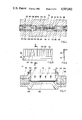
- FIGS. 4 through 9 the structure of apparatus 10 is disclosed. Thereby use is made of two bearers 86 and 88. In between these bearers successive segment packages 66 such as transporters for the substrates are positioned, so as to create passage 22. The notches 90 of segments 92, see also FIG. 6, rest in the corresponding grooves 94, positioned in the bearers 86 and 88, with a resulting precise width of the passage 22 for the substrates.
- the gaseous supply- and discharge channels are approximately the same. Thereby the entrances 104 of the supply channels are connected with the grooves 106 and 108, located in bearer 86, whereas these grooves, through supply channels 110 are connected with a discharge line (not illustrated).
- Covers 120 and 122 interconnect both bearers 86 and 88 while simultaneously enclosing the package. For that purpose bolt connections 124 and 126 are used.
- FIG. 7 the apparatus 10 is shown in a cross-section of the processing module 64. Thereby the distance between the bearers is to a small extent enlarged.
- the upper cover 128 is provided with the wall sections 130 and 132, located at the inside of the bearers, whereas on the upper wall 134 thereof the cabin top 136 is mounted.
- the lower cover 138 can be the same as the upper cover, if on both sides of the substrate the same processing takes place. If however only in the top section processing occurs, then lower cover 138 is provided with the bottom 140.
- Both covers can be made of a material, which is suitable for processing, such as for a micro-wave oven material, which is micro-wave damping and for plasma etching an electrical insulation material. Furthermore, such a cover 128 can contain inner transverse walls 142, through which the process chambers 64 are isolated.
- both covers 120' and 122' of the segment packages 66' also contain the side walls 142' for the module chamber 64'.
- the processing module 14, as is shown in FIGS. 1 and 2, can be an oven, whereby in sections 144 thereof generators of micro-waves are located. These micro-waves may move from two such generators through chamber 64 towards the substrates.
- the number of chambers 64 can vary between a single one for simple processing and ten or more for complicated ovens for de-hydration, with a total processing time of 10-20 seconds.
- any other type of generator of process medium can be positioned.
- a plasma etch module 146 is shown in a simplified form, whereby through passage 148 gas is supplied and in section 150 plasma is generated, which under a high speed by means of electrode arrangements 152 and 154 is directed towards substrate 12. A discharge of gases takes place through passage 156.
- FIG. 11 another plasma etch module 146' is shown, whereby the generation of the plasma takes place outside within chamber 158 and the plasma under high speed is fed to the successive module chambers. Thereby through passage 160 a discharge of gases occurs.
- the modules can contain any type of scanning, such as magnetic, electro-static and even mechanic. Furthermore, during the processing the substrates 12 can make contact with electrode 154 and can, together with these electrodes, be connected with a grounding means of the module.
- the module 162 for ion implantation is shown, whereby from generator 164 an ion beam is fed through divider 166 and a common scanning section 168 whereafter five split beams are fed to the module chambers.
- each type of scanning for divider 166 and section 168 is possible.
- a supplementary scanning is applicable.
- such module can contain any type of electrical insulation, as required.
- this number of generators can vary between a single generator for all module chambers together and one generator per module chamber.
- the module can also function as an etcher with the etching of the substrate surface by means of these ions.
- processing electrodes can be located in the module and the substrates can be electrically charged or grounded.
- metallization of the substrate surface can take place.
- modules for doping modules for doping, oxidation of the substrate surface
- modules to urge developing medium towards the substrates to develop the photo sensitive coating layer, applied thereon modules for stripping of such layer and electron beam processing systems.
- sensors 172 are located as a means for regulation of the transport speed of the substrates and with the use of the free areas in between successive segment packages, see FIGS. 8 and 12.
- instruments for measuring and testing and sensors to control the processing can be located.
- the substrates move through the apparatus separately from each other, with some distance in between. However, it is also possible, that these substrates adjoin each other in the direction of substrate movement.
- a supply station can be part of a processing module, wherein a take-over device transports the supplied substrates towards a position in this module for processing.
- a second take-over device discharges these substrates to a receiving discharge station. Thereby a number of substrates can be brought to this processing position, whereby processing of these substrates takes place simultaneously.
- FIGS. 13 and 14 show in detail a part of the transport system of a module, with an one-sided processing of the substrates, passing through.
- processing under an extremely high vacuum as for instance lower than 1 ⁇ 10 -5 torr, takes place, whereby during certain types of processing, such as ion implantation and ion etching or ion milling to a great extent heat is supplied to the substrates.
- cover 174 the passage 176 is located, through which the processing medium and/or beams are directed towards substrates 12".
- the cover extends towards close to the substrate passage and whereby this passage is smaller than that of chamber 178, such that also with no substrate, being present, still a sufficient screening-off of the segment packages take place.
- electrodes 180 located underneath chamber 178, whereby processing medium, which is passed through this this chamber is attracted thereon.
- cover plates can be positioned.
- the supply of the transport gases takes place through supply channel 36", with a vacuum pressure of for instance 1 torr as supply pressure.
- a vacuum pressure of for instance 1 torr as supply pressure.
- Gaseous transport medium is discharged from the gaps 40" through discharge channels 182 between the cover 174 and the upper segment package 66", cabin passage 184 aside the substrates 12" and lower chamber 178 towards the cabin compartment 186. Thereby a high vacuum pump is connected with this compartment.
- the segment packages and the processing chambers in between might have a length of approximately 3 mm in the direction of substrate movement. Consequently, per module the number of packages can be very large depending on the type of processing. Thereby an ideal in between cooling of the substrates can be maintained.
Landscapes
- Physics & Mathematics (AREA)
- Engineering & Computer Science (AREA)
- Fluid Mechanics (AREA)
- Mechanical Engineering (AREA)
- Container, Conveyance, Adherence, Positioning, Of Wafer (AREA)
- Drying Of Semiconductors (AREA)
- ing And Chemical Polishing (AREA)
Abstract
Improved apparatus (10), including passage (22) for inter-cushion processing and transport of substrates (12) towards and from process modules (14) and (16) for main processing of said substrates (12) at non-atmospheric pressure in a series of successive process chambers (64), located in between successive processors/transporters (66), in which secondary processing and transport of said substrates (12) take place.
Description
This is a division of copending application Ser. NO. 598,549 filed as PCT NL83/00031, on Aug. 23, 1983, published as WO84/01084 on Mar. 15, 1983, §102(e) date on Mar. 19, 1984.
In the Dutch Patent Applications No's 8 103 979 and 8 200 753 of the applicant a transport system for substrates is disclosed, whereby these substrates are fed through a centrally positioned passage of a cabin and in that passage aside the substrate at least locally flowing gaseous medium establishes a floating transport of these substrates with at least almost no mechanical contact thereof with cabin components.
The apparatus according to the invention shows some improvements for the transport system towards and from in particular modules, which complicated processings under high vacuum take place and is mainly characterized by including means to at least locally establish an independent transport of the substrates by means of flowing gaseous medium, moving along these substrates.
A following positive characteristic is, that the gaseous medium, fed towards such substrates, is splitted up in a main flow in direction of substrate movement towards a discharge and a secondary flow, moving in opposite direction towards another discharge and with a lower speed. Consequently, the resulting thrust of these flows on the substrate is in the direction of substrate movement.
Furthermore, the difference in speed of the flows is obtained by, as seen in direction of movement of the substrates, different widths of the transporter system segments with the smallest width in the direction of substrate movement.
The substrate might be a tape, which during the processing is independently fed through the apparatus. Therefor, the test of this application is also applicable to such tapes.
The substrates have tolerances in thickness, flatness, roughness and bow. Consequently, with a constant width of the passage, both gap widths in between the substrates and the passage-wall sections of the transporter segments vary, resulting in a variable flowing speed of the gaseous medium, a variable thrust of the gaseous medium on the substrates and consequently a variable speed of the substrates.
The apparatus is now characterized, in that in the direction of substrate movement in between the transporter segment packages free areas are located for the positioning of sensors for regulation of the gaseous medium pressure in the passage depending upon on the quality of these substrates and the type of processing.
In the apparatus modules micro-wave oven drying, metallization, plasma etching, plasma stripping, plasma developing, ion implantation, oxidation, doping and other complicated processing may take place located chambers in between transporters and often together with a high vacuum. Therein the substrates are transported by a transport system, which is part of such modules.
A very positive characteristic is, that in direction of substrate movement the length of such processing chambers in between successive transporter segment packages is smaller than the length of the substrates, that the portion of the passage, located behind such chamber, provides a sufficient guidance for the substrates to correctly enter the passage in front of that chamber.
In particular "high current" ion implentation and micro-wave oven drying require a relatively long lasting processing.
An additional characteristic is that in the direction of substrate movement a number of successive chambers with the same type of processing are used, with in between transported segment packages and such packages are provided with a central passage for such substrates.
Due to the extremely low weight of the substrates per square inch, the pressure in the passages between successive module chambers can be very low and locally even near the high vacuum, which is used for such type of processing. Furthermore, in such a passage the same gaseous medium can be used as is required for the processing. Also, the module processing cabin can be used as a common, wide discharge channel.
Furthermore, until now with high vacuum modules the supply and discharge of substrates accomplished by means of mechanical transport systems or cassettes of substrates are brought into these processing modules. This results in a loss of time, which is due to the reduction of the atmospheric pressure to high vacuum, whether or not through a load lock.
A following very positive characteristic of the present invention that in the gaseous supply section of the transport system towards such a processing module the pressure of successive flows of gaseous medium drops incrementally per group of such flows towards at least close to the high vacuum.
Furthermore, in the discharge section of such a processing module the pressure increases upwardly from at least close to this high vacuum and incrementally higher per group of successive flows of gaseous medium. Thereby the many successive flows of gaseous medium in the direction of substrate movement establish, by means of numerous micro thrusts on such a substrate, a displacement thereof against the increasing pressure.
Furthermore, it is of importance, that the speed of the processing and consequently the speed of transport of the substrate during such processing remains as uniform as possible.
A following very positive characteristic of the apparatus is that thereby in front of and behind a series of processing modules or chambers the same type of gaseous medium is used in transport as in the processing module.
Furthermore, that thereby the length of such an arrangement of transporters is greater than half the length of the substrates.
As the transporters and processing modules use the same type of gaseous medium such a quantity of cooling medium can be fed into such transporters and discharged therefrom, that during processing the temperature of the substrates remains below an acceptable value.
Further positive characteristics of the apparatus follow from the description of the following Figures:
FIG. 1 shows in a simplified schematic configuration the apparatus according to the invention, including several processing modules.
FIG. 2 shows the apparatus according to FIG. 1 in a more detailed form.
FIG. 3 is an enlarged fragmentary transverse section detail of the transport system in a module of the apparatus according to FIG. 1.
FIG. 4 is an enlarged longitudinal section of the apparatus according to FIG. 1 with the transporters, positioned therein.
FIG. 5 is a fragmentary side view of a segment package of the transporters.
FIG. 6 is a cross-section taken along line 6--6 of the segments according to FIG. 5.
FIG. 7 is a transverse cross-section of a process chamber of a module.
FIG. 8 is a top plan, partially in longitudinal section of the apparatus according to FIG. 1 at the location of a series of processing chambers.
FIG. 9 is a longitudinal section of the apparatus according to FIG. 1 at the location of micro-wave oven modules.
FIG. 10 shows a processing module for plasma etching.
FIG. 11 is another module for such a plasma etching.
FIG. 12 is a longitudinal section of the apparatus at the location of a series of processing chambers of a module for ion implantation.
FIG. 13 is a fragmentary longitudinal section of such a module.
FIG. 14 is a fragmentary section, taken along line 14--14 of FIG. 13.
In FIG. 1 apparatus 10 for processing of substrates 12 is shown. These substrates can also be a tape.
In this apparatus use is made of the process modules 14 and 16, and whereby by means of take-over device 20 the substrates 12 are transported from cassette 18 towards passage 22 of the transport section 24 for these modules.
Thereafter a displacement of the substrates takes place by means of flows of gaseous medium, which is fed from segment packages 26 into the passage 22 and urged along these substrates 12, see also FIG. 3.
In this transport section 24 in the successive stations 28, 30, 32 and 34 also successively cleaning, drying, rinsing and again drying takes place. For this and other simple continuous processing the possible use of the process systems, as is described in the Dutch Patent Applications No's 8 103 979 and 8 200 753 of the Applicant.
In FIG. 3 is shown, how also in or near these simple stations a transport of the substrates takes place regardless of processing medium.
Through supply channels 36 the gaseous medium 38 is urged towards the passage gaps 40 and 42 aside the substrates and whereby a discharge of such medium takes place through discharge channels 44. The segment 46 has a larger width than segment 48, with consequently a larger flow restriction in gap 50 as than in gap 52. As a result, in gap 52 the speed of the medium and therewith the force, applied on the substrate, is larger than that in gap 50 with a resulting force on the substrate in the direction of movement thereof. Due to the numerous flows of medium through successive series of channels a longitudinal displacement of the substrates is established.
In the module 14 processing under high vacuum takes place. For that purpose including transport section 54 in successive segment packages 56, 58, 60 and 62 gradually a drop in pressure of the transport medium occurs from near atmospheric pressure to near this high vacuum. Thereby use is made of supply- and discharge channels per segment package, wherein the pressure reduces per package. By means of a gradual increase of the flow restriction for the gaseous medium in the channels, located in such a package, the pressure in the gaps aside the substrates can also drop gradually.
The substrates are continuously fed through the module 14 while maintaining almost the same speed.
This module 14 consists of a great number of module chambers 64 with the transporters 66 positioned in between. Thereby these transporters 66 establish the displacement of the substrates through the module, whereby in the module chambers processing medium is urged towards such a substrate.
The structure of these transporters 66 is for instance shown in FIGS. 3 and 9. Thereby at least the first segments of the package are inclined to enable a correct entering of the substrates.
The length of the processing module chambers in between these transport segment packages is kept sufficiently small, that such a package provides sufficient guidance to the substate to pass through the following segment package without mechanical contact.
For a proper, even processing in this module 14 it is required, that the speed of the substrates through this module is constant, without being affected by the common, almost circular shape of the substrates. Therefor in the apparatus in front of this processing module 14 and behind it the respective transport stations 70 and 72 are located, in which the conditions of transport of the substrates are at least almost the same as those in the module. Thereby these transport stations can be provided with approximately the same segment packages 66 and the same areas 64 in between.
In cabin section 80, positioned in front of module 80, one or more simple basic processing steps can take place, after which the substrates by means of the take-over device 82 are transported towards cassette 84.
In FIGS. 4 through 9 the structure of apparatus 10 is disclosed. Thereby use is made of two bearers 86 and 88. In between these bearers successive segment packages 66 such as transporters for the substrates are positioned, so as to create passage 22. The notches 90 of segments 92, see also FIG. 6, rest in the corresponding grooves 94, positioned in the bearers 86 and 88, with a resulting precise width of the passage 22 for the substrates.
In segments 92 the main channel 96 is located, whereby a great number of branched channels 98 are connected therewith. The ends 100 of these channels 98 are in open connection with passage 22. In these channels 98 as supply channels the flow restriction for the gaseous medium is considerably larger than the restriction of the gap sections of the longitudinal passage aside the substrate. Consequently, even in the local absence of a substrate the flow of medium in the passage remains very limited.
By means of the mounting holes 102, located in these segments, and through which mounting means can be passed, a stacking of the segments is obtained under the creation of package 66.
The gaseous supply- and discharge channels are approximately the same. Thereby the entrances 104 of the supply channels are connected with the grooves 106 and 108, located in bearer 86, whereas these grooves, through supply channels 110 are connected with a discharge line (not illustrated).
In FIG. 7 the apparatus 10 is shown in a cross-section of the processing module 64. Thereby the distance between the bearers is to a small extent enlarged. The upper cover 128 is provided with the wall sections 130 and 132, located at the inside of the bearers, whereas on the upper wall 134 thereof the cabin top 136 is mounted.
The lower cover 138 can be the same as the upper cover, if on both sides of the substrate the same processing takes place. If however only in the top section processing occurs, then lower cover 138 is provided with the bottom 140.
Both covers can be made of a material, which is suitable for processing, such as for a micro-wave oven material, which is micro-wave damping and for plasma etching an electrical insulation material. Furthermore, such a cover 128 can contain inner transverse walls 142, through which the process chambers 64 are isolated.
In FIG. 9 the processing module 14 is shown in a more detailed configuration. Thereby both covers 120' and 122' of the segment packages 66' also contain the side walls 142' for the module chamber 64'.
The processing module 14, as is shown in FIGS. 1 and 2, can be an oven, whereby in sections 144 thereof generators of micro-waves are located. These micro-waves may move from two such generators through chamber 64 towards the substrates.
For this oven use can be made of micro-wave adsorbent material to prevent as much as possible a heating of module components and in particular the segment packages. Thereby, depending upon the type of oven and the transport speed of the substrates the number of chambers 64 can vary between a single one for simple processing and ten or more for complicated ovens for de-hydration, with a total processing time of 10-20 seconds.
In such generator sections 144 any other type of generator of process medium can be positioned.
In FIG. 10 a plasma etch module 146 is shown in a simplified form, whereby through passage 148 gas is supplied and in section 150 plasma is generated, which under a high speed by means of electrode arrangements 152 and 154 is directed towards substrate 12. A discharge of gases takes place through passage 156.
In FIG. 11 another plasma etch module 146' is shown, whereby the generation of the plasma takes place outside within chamber 158 and the plasma under high speed is fed to the successive module chambers. Thereby through passage 160 a discharge of gases occurs.
In these designs on behalf of processing the modules can contain any type of scanning, such as magnetic, electro-static and even mechanic. Furthermore, during the processing the substrates 12 can make contact with electrode 154 and can, together with these electrodes, be connected with a grounding means of the module.
In FIG. 12 the module 162 for ion implantation is shown, whereby from generator 164 an ion beam is fed through divider 166 and a common scanning section 168 whereafter five split beams are fed to the module chambers. Here also, each type of scanning for divider 166 and section 168 is possible. Furthermore, a supplementary scanning is applicable. Also, such module can contain any type of electrical insulation, as required.
Furthermore, as two generators 164 are shown, within the scope of the invention this number of generators can vary between a single generator for all module chambers together and one generator per module chamber.
The module can also function as an etcher with the etching of the substrate surface by means of these ions.
Furthermore, on behalf of processing electrodes can be located in the module and the substrates can be electrically charged or grounded.
In another configuration of the processing modules metallization of the substrate surface can take place.
Furthermore, within the scope of the invention all other types of processing are applicable, as for instance modules for doping, oxidation of the substrate surface, modules to urge developing medium towards the substrates to develop the photo sensitive coating layer, applied thereon, modules for stripping of such layer and electron beam processing systems.
Also, by means of media, flowing through these segment packages, an in between cooling of the substrates can take place and to such an extent, that during the processing temperature of the substrate cannot rise too high. Thereby an efficient use can be made of the transport medium as a cooling agent, as is shown in FIG. 4.
Furthermore, in the apparatus 10 sensors 172 are located as a means for regulation of the transport speed of the substrates and with the use of the free areas in between successive segment packages, see FIGS. 8 and 12.
Furthermore, in these areas or somewhere else in the apparatus, instruments for measuring and testing and sensors to control the processing can be located.
As is shown, the substrates move through the apparatus separately from each other, with some distance in between. However, it is also possible, that these substrates adjoin each other in the direction of substrate movement.
Furthermore, a supply station can be part of a processing module, wherein a take-over device transports the supplied substrates towards a position in this module for processing. A second take-over device discharges these substrates to a receiving discharge station. Thereby a number of substrates can be brought to this processing position, whereby processing of these substrates takes place simultaneously.
FIGS. 13 and 14 show in detail a part of the transport system of a module, with an one-sided processing of the substrates, passing through. In such a module processing under an extremely high vacuum, as for instance lower than 1×10⁻⁵ torr, takes place, whereby during certain types of processing, such as ion implantation and ion etching or ion milling to a great extent heat is supplied to the substrates.
However, by means of the gaseous medium, flowing through the segments and such eventually supplemented by cooling of these segments by such or another medium, a sufficient in between cooling of these substrates can be maintained.
In cover 174 the passage 176 is located, through which the processing medium and/or beams are directed towards substrates 12". The cover extends towards close to the substrate passage and whereby this passage is smaller than that of chamber 178, such that also with no substrate, being present, still a sufficient screening-off of the segment packages take place. Such also because of the possible use of electrodes 180, located underneath chamber 178, whereby processing medium, which is passed through this this chamber is attracted thereon. Furthermore, also in the chamber 178 aside the segment packages cover plates can be positioned.
The supply of the transport gases takes place through supply channel 36", with a vacuum pressure of for instance 1 torr as supply pressure. Thereby the floating of the substrates in the passage with the establishing of the gaps 40" and 42" is obtained by means of a lower supply pressure for the upper channels 36" or the including of a larger flow restriction in these upper channels.
Gaseous transport medium is discharged from the gaps 40" through discharge channels 182 between the cover 174 and the upper segment package 66", cabin passage 184 aside the substrates 12" and lower chamber 178 towards the cabin compartment 186. Thereby a high vacuum pump is connected with this compartment.
Furthermore, an immediate discharge of the transport gases from gap 42" takes place through the chamber 178. Eventually, here also a cover can be used with discharge channels in between this cover and the lower packages.
The consumption of transport gas, which is also used for the procession, is very restricted. Consequently, with no substrate present in the processing area 188, these gases can still sufficiently be discharged by the vacuum pumps.
The segment packages and the processing chambers in between might have a length of approximately 3 mm in the direction of substrate movement. Consequently, per module the number of packages can be very large depending on the type of processing. Thereby an ideal in between cooling of the substrates can be maintained.
Within the scope of the invention other configurations of the modules are possible.
Claims (46)
1. Apparatus for floating transport and processing of substrates comprising:
(a) an elongated cabin defining a longitudinal passage for moving substrates;
(b) at leat one processing module surrounding and in communication with said longitudinal passage;
(c) a supply of pressurized gaseous transport and processing medium for said substrates communicating with the top and bottom of said longitudinal passage via successive pluralities of transversely arrayed gaseous medium supply ports interconnecting said longitudinal passage; and
(d) a plurality of gaseous medium discharge ports intersecting the top and bottom of said passage in front of and behind each said gaseous medium supply passage, such that primary flow and secondary flow of gaseous medium is achieved in said passage.
2. Apparatus for floating transport and processing of substrates as in claim 1, wherein said gaseous medium discharge ports behind said supply ports are closer to said supply ports than the gaseous medium discharge ports in front of said supply ports.
3. Apparatus for floating transport and processing of substrates as in claim 2, including means for feeding such substrates from a cassette into said passage and means for discharging said substrates from said passage into a receiver.
4. Apparatus for floating transport and processing of substrates as in claim 1, wherein said successive gaseous medium supply ports and said gaseous medium discharge ports are arrayed on both sides of said longitudinal passage in pairs of spaced transport segment packages.
5. Apparatus for floating transport and processing of substrates as in claim 4, wherein said processing module includes a cleaning section and a drying section on both sides of said passage at successive spaces.
6. Apparatus for floating gaseous transport and processing of substrates as in claim 1, wherein said processing module encloses a plurality of longitudinally spaced pairs of transport segment packages such that main processing of said substrates is carried out in increments between said pairs of transport segment packages, wherein gaseous transport medium as a secondary processing medium is introduced and discharged.
7. Apparatus for floating gaseous transport and processing of substrates as in claim 5, wherein the length of said processing chambers is less than the length of said substrates, such that in said transport segment packages continuous floating guidance for substrates is maintained as said substrate proceeds from one processing chamber to another.
8. Apparatus for floating transport and processing of substrates as in claim 7, wherein the number of processing chambers intermediate pairs of transporter packages is such that the allowable temperature for said substrates is not surpassed.
9. Apparatus for floating gaseous transport and processing substrates as in claim 8, wherein the width of said processing chamber is greater than the width of said longitudinal passage in said transporter packages.
10. Apparatus for floating gaseous transport and processing of substrates as in claim 9, wherein said processing module includes transporter packages, partly made of electric insulating material.
11. Apparatus for floating gaseous transport and processing of substrates as in claim 8, wherein the transport medium as processing medium charged into said successive transporter packages, is of a lower temperature than the surface of the substrates leaving the processing chambers.
12. Apparatus for floating gaseous transport and processing of substrates as in claim 11, wherein each of said transporter packages includes at least one supply channel for cooling medium.
13. Apparatus for floating gaseous transport and processing of substrates as in claim 12, wherein said cooling medium is the same as the gaseous transport medium within the transporter packages.
14. Apparatus for floating gaseous transport and processing of substrates as in claim 11, wherein said transport medium is introduced into said transporter packages by means of a main supply channel connected to a plurality of branched channels transversely arrayed across the longitudinal passage.
15. Apparatus for floating gaseous transport and processing of substrates as in claim 14, wherein a main processing supply channel supplies a plurality of processing chambers intermediate said transporter segment packages.
16. Apparatus for floating transport and processing of substrates as in claim 15, wherein a beam divider is located within said processing module such that at least two beams are directed towards said longitudinal passage intermediate transporter segment packages and onto said substrates.
17. Apparatus for floating gaseous transport and processing of substrates as in claim 16, wherein the beams are fed through electrostatic scanning means to obtain flat beams with a width in the direction of movement of said substrates which is smaller than the length of the processing chambers intermediate transporter segment packages.
18. Apparatus for floating transport and processing of substrates as in claim 17, wherein said beams are fed through magnetic scanning means to obtain flat beams with a width in the direction of movement of said substrates which is smaller than the length of the processing chambers intermediate transporter segment packages.
19. Apparatus for floating transport and processing of substrates as in claim 15, wherein a generator of microwaves for heating the substrates is supported.
20. Apparatus for floating transport and processing of substrates as in claim 19, wherein the cover of said processing module is made of microwave absorbent material such that openings are restricted to passing through of microwaves from the generator towards the processing chambers intermediate the transporter segment packages.
21. Apparatus for floating transport and processing of substrates as in claim 15, including an ion generator for ion implantation in said substrates.
22. Apparatus for floating gaseous transport and processing of substrates as in claim 15, including an ion generator for etching of substrates.
23. Apparatus for floating gaseous transport and processing of substrates as in claim 15, including a target for metallization of said substrate surface.
24. Apparatus for floating gaseous transport and processing of substrates as in claim 15, wherein said processing chambers contain means for doping of the substrate surface.
25. Apparatus for floating gaseous transport and processing of substrates as in claim 15, wherein said processing chambers include means for oxidation of the substrate surfaces.
26. Apparatus for floating gaseous transport and processing of substrates as in claim 15, wherein said processing modules include means for electrically charging said substrates.
27. Apparatus for floating gaseous transport and processing of substrates as in claim 15, wherein said processing module is electrically charged and includes oppositely charged shields extending towards the substrate passage.
28. Apparatus for floating gaseous transport and processing of substrates as in claim 27, wherein an electrode is located on the non-processing side of said longitudinal passage adjacent said processing module.
29. Apparatus for floating gaseous transport and processing of substrates in claim 28, wherein said electrode has a length in the direction of substrate movement which corresponds to the length of the transporter segment package with said processing module.
30. Apparatus for floating gaseous transport and processing of substrates as in claim 29, wherein said electrode is electrically grounded.
31. Apparatus for floating gaseous transport and processing of substrates as in claim 15, wherein two bearers extend aside said passage in the direction of substrate movement and in between said bearers processing chambers and transporter segment packages are located together with covers which enclose said transporter packages in transverse direction of said module.
32. Apparatus for floating gaseous transport and processing of substrates as in claim 31, wherein said covers are in the form of walls aside said processing chambers and the ends thereof are part of the longitudinal passage for the substrates.
33. Apparatus for floating gaseous transport and processing of substrates as in claim 32, wherein a main gaseous medium supply channel is located in each of two sections of said transporter packages with a number of branch channels leading into said longitudinal passage, said branch channels including a narrowing as a flow restriction for gaseous transport medium.
34. Apparatus for gaseous transport and processing of substrates as in claim 33, including in between said sections and said covers discharge channels for gaseous medium leading from said two sections.
35. Apparatus for floating gaseous transport and processing of substrates as in claim 34, wherein in at least one of said processing chambers processing takes place on both sides of said substrate.
36. Apparatus for floating gaseous transport and processing of substrates as in claim 34, wherein in said transporter segment packages the pressure of said gaseous transport medium beneath said substrates is greater than the pressure of said gaseous medium above said substrates.
37. Apparatus for floating gaseous transport and processing of substrates as in claim 36, wherein on at least the processing side of said longitudinal passage high vacuum discharge channels are part of said transporter segment packages.
38. Apparatus for floating gaseous transport and processing of substrates as in claim 32, wherein said cover includes sidewall section shielding off the sidewalls of the cabin aside the processing chambers, said sidewall also extending towards the substrate passage.
39. Apparatus for floating gaseous transport and processing of substrates as in claim 38, wherein by means of said covers the processing side of said chamber is in open connection with the non-processing side thereof.
40. Apparatus for floating gaseous transport and processing of substrates as in claim 39, wherein within said processing chamber the distance between the sidewalls of the cabin is greater than the width of the substrates and a communication compartment is located interconnecting the processing side of the module with the non-processing side.
41. Apparatus for floating gaseous transport and processing of substrates as in claim 40, wherein on the processing side of said passage high vacuum discharge channels are located in between said transport medium supply channels and said covers.
42. Apparatus for floating gaseous transport and processing of substrates as in claim 40, wherein said processing module includes a communication department connected to a central discharge high vacuum pump.
43. Apparatus for floating gaseous transport and processing of substrates as in claim 42, wherein a number of cathodes located for metallization of the substrate are located within the processing department, said cathodes having a width which is at least as great as the width of the substrates.
44. Apparatus for floating gaseous transport and processing of substrates as in claim 43, wherein said processing compartment includes at least one target as a supplier of materials for said substrates.
45. Apparatus for floating gaseous transport and processing of substrates as in claim 5 including means for a pressure drop to a vacuum.
46. Apparatus for floating gaseous transport and processing of substrates as in claim 5 including means for a pressure rise from a vacuum.
Applications Claiming Priority (2)
| Application Number | Priority Date | Filing Date | Title |
|---|---|---|---|
| NL8203318 | 1982-08-24 | ||
| NL8203318A NL8203318A (en) | 1982-08-24 | 1982-08-24 | DEVICE FOR PROCESSING SUBSTRATES. |
Related Parent Applications (1)
| Application Number | Title | Priority Date | Filing Date |
|---|---|---|---|
| US06/598,549 Division US4575408A (en) | 1982-08-24 | 1983-08-23 | Method for floating transport of substrates |
Publications (1)
| Publication Number | Publication Date |
|---|---|
| US4587002A true US4587002A (en) | 1986-05-06 |
Family
ID=19840175
Family Applications (2)
| Application Number | Title | Priority Date | Filing Date |
|---|---|---|---|
| US06/598,549 Expired - Fee Related US4575408A (en) | 1982-08-24 | 1983-08-23 | Method for floating transport of substrates |
| US06/736,587 Expired - Fee Related US4587002A (en) | 1982-08-24 | 1985-05-21 | Apparatus for floating transport and processing of substrate or tape |
Family Applications Before (1)
| Application Number | Title | Priority Date | Filing Date |
|---|---|---|---|
| US06/598,549 Expired - Fee Related US4575408A (en) | 1982-08-24 | 1983-08-23 | Method for floating transport of substrates |
Country Status (5)
| Country | Link |
|---|---|
| US (2) | US4575408A (en) |
| EP (1) | EP0116612A1 (en) |
| JP (1) | JPS59501727A (en) |
| NL (1) | NL8203318A (en) |
| WO (1) | WO1984001084A1 (en) |
Cited By (50)
| Publication number | Priority date | Publication date | Assignee | Title |
|---|---|---|---|---|
| US4717461A (en) * | 1986-09-15 | 1988-01-05 | Machine Technology, Inc. | System and method for processing workpieces |
| US4722298A (en) * | 1986-05-19 | 1988-02-02 | Machine Technology, Inc. | Modular processing apparatus for processing semiconductor wafers |
| US4806225A (en) * | 1982-05-28 | 1989-02-21 | Advanced Plasma Systems, Inc. | Desmearing and plated-through-hole apparatus |
| US4839145A (en) * | 1986-08-27 | 1989-06-13 | Massachusetts Institute Of Technology | Chemical vapor deposition reactor |
| US4863577A (en) * | 1982-05-28 | 1989-09-05 | Advanced Plasma Systems, Inc. | Desmearing and plated-through-hole method |
| US4889609A (en) * | 1988-09-06 | 1989-12-26 | Ovonic Imaging Systems, Inc. | Continuous dry etching system |
| US4911810A (en) * | 1988-06-21 | 1990-03-27 | Brown University | Modular sputtering apparatus |
| US5013385A (en) * | 1986-04-18 | 1991-05-07 | General Signal Corporation | Quad processor |
| US5076204A (en) * | 1988-09-29 | 1991-12-31 | Nec Corporation | Apparatus for producing semiconductor device |
| US5076205A (en) * | 1989-01-06 | 1991-12-31 | General Signal Corporation | Modular vapor processor system |
| US5102495A (en) * | 1986-04-18 | 1992-04-07 | General Signal Corporation | Method providing multiple-processing of substrates |
| US5248371A (en) * | 1992-08-13 | 1993-09-28 | General Signal Corporation | Hollow-anode glow discharge apparatus |
| US5308431A (en) * | 1986-04-18 | 1994-05-03 | General Signal Corporation | System providing multiple processing of substrates |
| US5340454A (en) * | 1991-04-09 | 1994-08-23 | Leybold Aktiengesellschaft | Method and apparatus for the coating of substrates |
| US5344542A (en) * | 1986-04-18 | 1994-09-06 | General Signal Corporation | Multiple-processing and contamination-free plasma etching system |
| US5409387A (en) * | 1993-08-17 | 1995-04-25 | Berg Technology, Inc. | Connector with passive switch for electrostatic discharge |
| US5562800A (en) * | 1993-09-20 | 1996-10-08 | Hitachi, Ltd. | Wafer transport method |
| US6103055A (en) * | 1986-04-18 | 2000-08-15 | Applied Materials, Inc. | System for processing substrates |
| US6239038B1 (en) | 1995-10-13 | 2001-05-29 | Ziying Wen | Method for chemical processing semiconductor wafers |
| US6241427B1 (en) * | 1998-11-20 | 2001-06-05 | Seagate Technology, Inc. | System and method for substantially touchless hydrodynamic transport of objects |
| US20080317956A1 (en) * | 2005-09-23 | 2008-12-25 | Fraunhofer-Gesellschaft Zur Forderung Der Angewandten Forschung E.V. | Device and Method for Continuous Chemical Vapour Deposition Under Atmospheric Pressure and Use Thereof |
| US20090324379A1 (en) * | 2008-05-30 | 2009-12-31 | Alta Devices, Inc. | Methods and apparatus for a chemical vapor deposition reactor |
| NL1037060C2 (en) * | 2009-06-23 | 2010-12-27 | Edward Bok | SEMICONDUCTOR INSTALLATION, INCLUDING AT LEAST A LONG NARROW SEMICONDUCTOR SUBSTRATE TRANSFER / TUNNING TUNNEL SETUP FOR THE FUNCTIONING OF THE UNINTERRUPTED PLACE OF A TOTAL SEMICONDUCTOR DISCONTINUATION OF DISCONTINUATION OF DISCONTINUATION OF DISCLAIMER. |
| NL1037068C2 (en) * | 2009-06-23 | 2010-12-27 | Edward Bok | SEMICONDUCTOR SUBSTRATE TRANSFER / treatment-TUNNEL ESTABLISHMENT WHICH IN ITS OPERATION IN MULTIPLE STRIP SHAPE UP SPLIT-SECTIONS IT ABOVE THE SUCCESSIVE, UNINTERRUPTED BENEATH ALONG moving SEMICONDUCTOR SUBSTRATE-SECTIONS UNINTERRUPTED PLACE OF HEAT TREATMENT UNDER VIBRATION CONDITION OF IT IN THE PRECEDING PORTION THEREOF applied LAYER OF THE COMBINATION OF LIQUID CARRYING MEDIUM AND PARTICLES OF A SEMICONDUCTOR SUBSTANCE. |
| NL1037061C2 (en) * | 2009-06-23 | 2010-12-27 | Edward Bok | SEMICONDUCTOR FACILITY, CONTAINING AT LEAST ONE VERY LONG NARROW SEMICONDUCTOR SUBSTRATE TRANSFER / TREATMENT INSTALLATION. |
| US20110124199A1 (en) * | 2008-05-20 | 2011-05-26 | Granneman Ernst H A | Apparatus and method for high-throughput atomic layer deposition |
| US20110268879A1 (en) * | 2008-05-20 | 2011-11-03 | Granneman Ernst H A | Apparatus and method for high-throughput atomic layer deposition |
| WO2011145918A1 (en) * | 2010-05-18 | 2011-11-24 | Edward Bok | Semiconductor installation, containing at-least also a long narrow semiconductor substrate transfer / processing tunnel-arrangement to during its operation the uninterruptedly taking place of a total semiconductor processing / treatment- process of the therein displacing semiconductor substrates |
| EP2481830A1 (en) * | 2011-01-31 | 2012-08-01 | Nederlandse Organisatie voor toegepast -natuurwetenschappelijk onderzoek TNO | Apparatus for atomic layer deposition. |
| US20120196050A1 (en) * | 2009-07-30 | 2012-08-02 | Adrianus Johannes Petrus Maria Vermeer | Apparatus and method for atomic layer deposition |
| US20120291707A1 (en) * | 2009-11-19 | 2012-11-22 | Levitech B.V. | Floating wafer track with lateral stabilization mechanism |
| US20140037847A1 (en) * | 2011-01-31 | 2014-02-06 | Adrianus Johannes Petrus Maria Vermeer | Apparatus and method for atomic layer deposition |
| US20150086729A1 (en) * | 2012-04-03 | 2015-03-26 | Solaytec B.V. | Method for producing a substrate with stacked deposition layers |
| US9297077B2 (en) | 2010-02-11 | 2016-03-29 | Nederlandse Organisatie Voor Toegepast-Natuurwetenschappelijk Onderzoek Tno | Method and apparatus for depositing atomic layers on a substrate |
| EP2102383B1 (en) | 2007-01-08 | 2017-01-25 | Eastman Kodak Company | Process FOR THIN FILM DEPOSITION |
| TWI571919B (en) * | 2011-01-31 | 2017-02-21 | 荷蘭Tno自然科學組織公司 | Apparatus for atomic layer deposition |
| US9761458B2 (en) | 2010-02-26 | 2017-09-12 | Nederlandse Organisatie Voor Toegepast-Natuurwetenschappelijk Onderzoek Tno | Apparatus and method for reactive ion etching |
| WO2017153356A1 (en) | 2016-03-07 | 2017-09-14 | Fofitec Ag | Device for depositing thin layers |
| EP3138123A4 (en) * | 2014-04-30 | 2018-01-17 | Kateeva, Inc. | Gas cushion apparatus and techniques for substrate coating |
| US20180231952A1 (en) * | 2017-02-14 | 2018-08-16 | SCREEN Holdings Co., Ltd. | Substrate transport device, substrate processing apparatus including the substrate transport device, and substrate transport method |
| US10351954B2 (en) | 2007-01-08 | 2019-07-16 | Eastman Kodak Company | Deposition system and method using a delivery head separated from a substrate by gas pressure |
| US10512931B2 (en) | 2014-01-21 | 2019-12-24 | Kateeva, Inc. | Apparatus and techniques for electronic device encapsulation |
| US11107712B2 (en) | 2013-12-26 | 2021-08-31 | Kateeva, Inc. | Techniques for thermal treatment of electronic devices |
| US11230757B2 (en) | 2008-06-13 | 2022-01-25 | Kateeva, Inc. | Method and apparatus for load-locked printing |
| US11489119B2 (en) | 2014-01-21 | 2022-11-01 | Kateeva, Inc. | Apparatus and techniques for electronic device encapsulation |
| US11549180B2 (en) * | 2008-08-27 | 2023-01-10 | Nederlandse Organisatie Voor Toegepast-Natuurwetenschappelijk Onderzoek Tno | Apparatus and method for atomic layer deposition |
| US11633968B2 (en) | 2008-06-13 | 2023-04-25 | Kateeva, Inc. | Low-particle gas enclosure systems and methods |
| US11975546B2 (en) | 2008-06-13 | 2024-05-07 | Kateeva, Inc. | Gas enclosure assembly and system |
| US12018857B2 (en) | 2008-06-13 | 2024-06-25 | Kateeva, Inc. | Gas enclosure assembly and system |
| US12064979B2 (en) | 2008-06-13 | 2024-08-20 | Kateeva, Inc. | Low-particle gas enclosure systems and methods |
Families Citing this family (322)
| Publication number | Priority date | Publication date | Assignee | Title |
|---|---|---|---|---|
| NL8300649A (en) * | 1983-02-21 | 1984-09-17 | Integrated Automation | METHOD AND APPARATUS FOR APPLYING A COATING TO A SUBSTRATE OR TAPE. |
| NL8302163A (en) * | 1983-06-16 | 1985-01-16 | Bok Edward | IMPROVED PROCESS INSTALLATION WITH FLOATING TRANSPORT OF SUBSTRATES. |
| JPS6074626A (en) * | 1983-09-30 | 1985-04-26 | Fujitsu Ltd | Device for plasma treatment |
| NL8400658A (en) * | 1984-03-01 | 1985-10-01 | Bok Edward | IMPROVED INSTALLATION FOR VACUUM PROCESSING OF SUBSTRATES. |
| NL8401776A (en) * | 1984-06-04 | 1986-01-02 | Bok Edward | IMPROVED DOUBLE-FLOATING WAFER TRANSPORT / PROCESSING INSTALLATION. |
| FR2574221B1 (en) * | 1984-12-05 | 1988-06-24 | Montaudon Patrick | METHOD AND DEVICE FOR THE CHEMICAL ATTACK ON A SINGLE SIDE OF A SUBSTRATE |
| JPS61174639A (en) * | 1985-01-28 | 1986-08-06 | Semiconductor Energy Lab Co Ltd | Method of photo etching |
| US5082747A (en) * | 1985-11-12 | 1992-01-21 | Hedgcoth Virgle L | Magnetic recording disk and sputtering process and apparatus for producing same |
| FR2590554B1 (en) * | 1985-11-27 | 1989-08-11 | Kishimoto Sangyo Co | PACKAGING-CONTAINER |
| EP0261145A1 (en) * | 1986-02-03 | 1988-03-30 | BOK, Edward | Installation for floating transport and processing of wafers |
| JPS63128710A (en) * | 1986-11-19 | 1988-06-01 | Mitsubishi Electric Corp | Reaction furnace |
| US5871811A (en) * | 1986-12-19 | 1999-02-16 | Applied Materials, Inc. | Method for protecting against deposition on a selected region of a substrate |
| US5868854A (en) * | 1989-02-27 | 1999-02-09 | Hitachi, Ltd. | Method and apparatus for processing samples |
| US6989228B2 (en) * | 1989-02-27 | 2006-01-24 | Hitachi, Ltd | Method and apparatus for processing samples |
| US6077788A (en) * | 1989-02-27 | 2000-06-20 | Hitachi, Ltd. | Method and apparatus for processing samples |
| JP2528962B2 (en) * | 1989-02-27 | 1996-08-28 | 株式会社日立製作所 | Sample processing method and device |
| JP2683940B2 (en) * | 1989-08-09 | 1997-12-03 | 信越半導体 株式会社 | Automatic work cleaning device |
| US5230741A (en) * | 1990-07-16 | 1993-07-27 | Novellus Systems, Inc. | Gas-based backside protection during substrate processing |
| US5578532A (en) * | 1990-07-16 | 1996-11-26 | Novellus Systems, Inc. | Wafer surface protection in a gas deposition process |
| US5133284A (en) * | 1990-07-16 | 1992-07-28 | National Semiconductor Corp. | Gas-based backside protection during substrate processing |
| US5238499A (en) * | 1990-07-16 | 1993-08-24 | Novellus Systems, Inc. | Gas-based substrate protection during processing |
| US5843233A (en) * | 1990-07-16 | 1998-12-01 | Novellus Systems, Inc. | Exclusion guard and gas-based substrate protection for chemical vapor deposition apparatus |
| US5620525A (en) * | 1990-07-16 | 1997-04-15 | Novellus Systems, Inc. | Apparatus for supporting a substrate and introducing gas flow doximate to an edge of the substrate |
| JP3351802B2 (en) * | 1991-01-01 | 2002-12-03 | 忠弘 大見 | Thin film forming equipment |
| US5651868A (en) * | 1994-10-26 | 1997-07-29 | International Business Machines Corporation | Method and apparatus for coating thin film data storage disks |
| NL1003538C2 (en) * | 1996-07-08 | 1998-01-12 | Advanced Semiconductor Mat | Method and device for contactless treatment of a disc-shaped semiconductor substrate. |
| US6183565B1 (en) | 1997-07-08 | 2001-02-06 | Asm International N.V | Method and apparatus for supporting a semiconductor wafer during processing |
| NL1011856C2 (en) * | 1999-04-21 | 2000-10-24 | Asm Internat B V | Floating wafer reactor as well as method for controlling its temperature. |
| NL1012004C2 (en) | 1999-05-07 | 2000-11-13 | Asm Int | Method for moving wafers as well as ring. |
| NL1018086C2 (en) * | 2001-05-16 | 2002-11-26 | Asm Int | Method and device for the thermal treatment of substrates. |
| US20030168174A1 (en) | 2002-03-08 | 2003-09-11 | Foree Michael Todd | Gas cushion susceptor system |
| US7104578B2 (en) * | 2002-03-15 | 2006-09-12 | Asm International N.V. | Two level end effector |
| US7181132B2 (en) | 2003-08-20 | 2007-02-20 | Asm International N.V. | Method and system for loading substrate supports into a substrate holder |
| US7022627B2 (en) | 2003-10-31 | 2006-04-04 | Asm International N.V. | Method for the heat treatment of substrates |
| US7410355B2 (en) * | 2003-10-31 | 2008-08-12 | Asm International N.V. | Method for the heat treatment of substrates |
| US6940047B2 (en) * | 2003-11-14 | 2005-09-06 | Asm International N.V. | Heat treatment apparatus with temperature control system |
| US7217670B2 (en) * | 2004-11-22 | 2007-05-15 | Asm International N.V. | Dummy substrate for thermal reactor |
| US8349196B2 (en) * | 2007-12-06 | 2013-01-08 | Intevac, Inc. | System and method for commercial fabrication of patterned media |
| KR101296659B1 (en) * | 2008-11-14 | 2013-08-14 | 엘지디스플레이 주식회사 | Washing device |
| US20130023129A1 (en) | 2011-07-20 | 2013-01-24 | Asm America, Inc. | Pressure transmitter for a semiconductor processing environment |
| US10714315B2 (en) | 2012-10-12 | 2020-07-14 | Asm Ip Holdings B.V. | Semiconductor reaction chamber showerhead |
| US20160376700A1 (en) | 2013-02-01 | 2016-12-29 | Asm Ip Holding B.V. | System for treatment of deposition reactor |
| US11015245B2 (en) | 2014-03-19 | 2021-05-25 | Asm Ip Holding B.V. | Gas-phase reactor and system having exhaust plenum and components thereof |
| US10858737B2 (en) | 2014-07-28 | 2020-12-08 | Asm Ip Holding B.V. | Showerhead assembly and components thereof |
| US10332770B2 (en) * | 2014-09-24 | 2019-06-25 | Sandisk Technologies Llc | Wafer transfer system |
| US10941490B2 (en) | 2014-10-07 | 2021-03-09 | Asm Ip Holding B.V. | Multiple temperature range susceptor, assembly, reactor and system including the susceptor, and methods of using the same |
| US10276355B2 (en) | 2015-03-12 | 2019-04-30 | Asm Ip Holding B.V. | Multi-zone reactor, system including the reactor, and method of using the same |
| US10458018B2 (en) | 2015-06-26 | 2019-10-29 | Asm Ip Holding B.V. | Structures including metal carbide material, devices including the structures, and methods of forming same |
| US10211308B2 (en) | 2015-10-21 | 2019-02-19 | Asm Ip Holding B.V. | NbMC layers |
| US11139308B2 (en) | 2015-12-29 | 2021-10-05 | Asm Ip Holding B.V. | Atomic layer deposition of III-V compounds to form V-NAND devices |
| US10529554B2 (en) | 2016-02-19 | 2020-01-07 | Asm Ip Holding B.V. | Method for forming silicon nitride film selectively on sidewalls or flat surfaces of trenches |
| US10343920B2 (en) | 2016-03-18 | 2019-07-09 | Asm Ip Holding B.V. | Aligned carbon nanotubes |
| US10367080B2 (en) | 2016-05-02 | 2019-07-30 | Asm Ip Holding B.V. | Method of forming a germanium oxynitride film |
| US11453943B2 (en) | 2016-05-25 | 2022-09-27 | Asm Ip Holding B.V. | Method for forming carbon-containing silicon/metal oxide or nitride film by ALD using silicon precursor and hydrocarbon precursor |
| US10074554B2 (en) | 2016-06-27 | 2018-09-11 | Tel Nexx, Inc. | Workpiece loader for a wet processing system |
| US10612137B2 (en) | 2016-07-08 | 2020-04-07 | Asm Ip Holdings B.V. | Organic reactants for atomic layer deposition |
| US9859151B1 (en) | 2016-07-08 | 2018-01-02 | Asm Ip Holding B.V. | Selective film deposition method to form air gaps |
| US9887082B1 (en) | 2016-07-28 | 2018-02-06 | Asm Ip Holding B.V. | Method and apparatus for filling a gap |
| US9812320B1 (en) | 2016-07-28 | 2017-11-07 | Asm Ip Holding B.V. | Method and apparatus for filling a gap |
| KR102532607B1 (en) | 2016-07-28 | 2023-05-15 | 에이에스엠 아이피 홀딩 비.브이. | Substrate processing apparatus and method of operating the same |
| US11532757B2 (en) | 2016-10-27 | 2022-12-20 | Asm Ip Holding B.V. | Deposition of charge trapping layers |
| US10714350B2 (en) | 2016-11-01 | 2020-07-14 | ASM IP Holdings, B.V. | Methods for forming a transition metal niobium nitride film on a substrate by atomic layer deposition and related semiconductor device structures |
| KR102546317B1 (en) | 2016-11-15 | 2023-06-21 | 에이에스엠 아이피 홀딩 비.브이. | Gas supply unit and substrate processing apparatus including the same |
| KR102762543B1 (en) | 2016-12-14 | 2025-02-05 | 에이에스엠 아이피 홀딩 비.브이. | Substrate processing apparatus |
| US11581186B2 (en) | 2016-12-15 | 2023-02-14 | Asm Ip Holding B.V. | Sequential infiltration synthesis apparatus |
| US11447861B2 (en) | 2016-12-15 | 2022-09-20 | Asm Ip Holding B.V. | Sequential infiltration synthesis apparatus and a method of forming a patterned structure |
| KR102700194B1 (en) | 2016-12-19 | 2024-08-28 | 에이에스엠 아이피 홀딩 비.브이. | Substrate processing apparatus |
| US10269558B2 (en) | 2016-12-22 | 2019-04-23 | Asm Ip Holding B.V. | Method of forming a structure on a substrate |
| US11390950B2 (en) | 2017-01-10 | 2022-07-19 | Asm Ip Holding B.V. | Reactor system and method to reduce residue buildup during a film deposition process |
| US10468261B2 (en) | 2017-02-15 | 2019-11-05 | Asm Ip Holding B.V. | Methods for forming a metallic film on a substrate by cyclical deposition and related semiconductor device structures |
| US10529563B2 (en) | 2017-03-29 | 2020-01-07 | Asm Ip Holdings B.V. | Method for forming doped metal oxide films on a substrate by cyclical deposition and related semiconductor device structures |
| US10770286B2 (en) | 2017-05-08 | 2020-09-08 | Asm Ip Holdings B.V. | Methods for selectively forming a silicon nitride film on a substrate and related semiconductor device structures |
| US12040200B2 (en) | 2017-06-20 | 2024-07-16 | Asm Ip Holding B.V. | Semiconductor processing apparatus and methods for calibrating a semiconductor processing apparatus |
| US11306395B2 (en) | 2017-06-28 | 2022-04-19 | Asm Ip Holding B.V. | Methods for depositing a transition metal nitride film on a substrate by atomic layer deposition and related deposition apparatus |
| KR20190009245A (en) | 2017-07-18 | 2019-01-28 | 에이에스엠 아이피 홀딩 비.브이. | Methods for forming a semiconductor device structure and related semiconductor device structures |
| US10541333B2 (en) | 2017-07-19 | 2020-01-21 | Asm Ip Holding B.V. | Method for depositing a group IV semiconductor and related semiconductor device structures |
| US11374112B2 (en) | 2017-07-19 | 2022-06-28 | Asm Ip Holding B.V. | Method for depositing a group IV semiconductor and related semiconductor device structures |
| US11018002B2 (en) | 2017-07-19 | 2021-05-25 | Asm Ip Holding B.V. | Method for selectively depositing a Group IV semiconductor and related semiconductor device structures |
| US10590535B2 (en) | 2017-07-26 | 2020-03-17 | Asm Ip Holdings B.V. | Chemical treatment, deposition and/or infiltration apparatus and method for using the same |
| TWI815813B (en) | 2017-08-04 | 2023-09-21 | 荷蘭商Asm智慧財產控股公司 | Showerhead assembly for distributing a gas within a reaction chamber |
| US10692741B2 (en) | 2017-08-08 | 2020-06-23 | Asm Ip Holdings B.V. | Radiation shield |
| US10770336B2 (en) | 2017-08-08 | 2020-09-08 | Asm Ip Holding B.V. | Substrate lift mechanism and reactor including same |
| US11139191B2 (en) | 2017-08-09 | 2021-10-05 | Asm Ip Holding B.V. | Storage apparatus for storing cassettes for substrates and processing apparatus equipped therewith |
| US11769682B2 (en) | 2017-08-09 | 2023-09-26 | Asm Ip Holding B.V. | Storage apparatus for storing cassettes for substrates and processing apparatus equipped therewith |
| US11830730B2 (en) | 2017-08-29 | 2023-11-28 | Asm Ip Holding B.V. | Layer forming method and apparatus |
| US11056344B2 (en) | 2017-08-30 | 2021-07-06 | Asm Ip Holding B.V. | Layer forming method |
| US11295980B2 (en) | 2017-08-30 | 2022-04-05 | Asm Ip Holding B.V. | Methods for depositing a molybdenum metal film over a dielectric surface of a substrate by a cyclical deposition process and related semiconductor device structures |
| KR102491945B1 (en) | 2017-08-30 | 2023-01-26 | 에이에스엠 아이피 홀딩 비.브이. | Substrate processing apparatus |
| US10658205B2 (en) | 2017-09-28 | 2020-05-19 | Asm Ip Holdings B.V. | Chemical dispensing apparatus and methods for dispensing a chemical to a reaction chamber |
| US10403504B2 (en) | 2017-10-05 | 2019-09-03 | Asm Ip Holding B.V. | Method for selectively depositing a metallic film on a substrate |
| US10923344B2 (en) | 2017-10-30 | 2021-02-16 | Asm Ip Holding B.V. | Methods for forming a semiconductor structure and related semiconductor structures |
| US11022879B2 (en) | 2017-11-24 | 2021-06-01 | Asm Ip Holding B.V. | Method of forming an enhanced unexposed photoresist layer |
| JP7214724B2 (en) | 2017-11-27 | 2023-01-30 | エーエスエム アイピー ホールディング ビー.ブイ. | Storage device for storing wafer cassettes used in batch furnaces |
| TWI791689B (en) | 2017-11-27 | 2023-02-11 | 荷蘭商Asm智慧財產控股私人有限公司 | Apparatus including a clean mini environment |
| US10872771B2 (en) | 2018-01-16 | 2020-12-22 | Asm Ip Holding B. V. | Method for depositing a material film on a substrate within a reaction chamber by a cyclical deposition process and related device structures |
| KR102695659B1 (en) | 2018-01-19 | 2024-08-14 | 에이에스엠 아이피 홀딩 비.브이. | Method for depositing a gap filling layer by plasma assisted deposition |
| TWI799494B (en) | 2018-01-19 | 2023-04-21 | 荷蘭商Asm 智慧財產控股公司 | Deposition method |
| US11081345B2 (en) | 2018-02-06 | 2021-08-03 | Asm Ip Holding B.V. | Method of post-deposition treatment for silicon oxide film |
| US11685991B2 (en) | 2018-02-14 | 2023-06-27 | Asm Ip Holding B.V. | Method for depositing a ruthenium-containing film on a substrate by a cyclical deposition process |
| US10896820B2 (en) | 2018-02-14 | 2021-01-19 | Asm Ip Holding B.V. | Method for depositing a ruthenium-containing film on a substrate by a cyclical deposition process |
| US10731249B2 (en) | 2018-02-15 | 2020-08-04 | Asm Ip Holding B.V. | Method of forming a transition metal containing film on a substrate by a cyclical deposition process, a method for supplying a transition metal halide compound to a reaction chamber, and related vapor deposition apparatus |
| KR102636427B1 (en) | 2018-02-20 | 2024-02-13 | 에이에스엠 아이피 홀딩 비.브이. | Substrate processing method and apparatus |
| US10975470B2 (en) | 2018-02-23 | 2021-04-13 | Asm Ip Holding B.V. | Apparatus for detecting or monitoring for a chemical precursor in a high temperature environment |
| US11473195B2 (en) | 2018-03-01 | 2022-10-18 | Asm Ip Holding B.V. | Semiconductor processing apparatus and a method for processing a substrate |
| US11629406B2 (en) | 2018-03-09 | 2023-04-18 | Asm Ip Holding B.V. | Semiconductor processing apparatus comprising one or more pyrometers for measuring a temperature of a substrate during transfer of the substrate |
| US11114283B2 (en) | 2018-03-16 | 2021-09-07 | Asm Ip Holding B.V. | Reactor, system including the reactor, and methods of manufacturing and using same |
| KR102646467B1 (en) | 2018-03-27 | 2024-03-11 | 에이에스엠 아이피 홀딩 비.브이. | Method of forming an electrode on a substrate and a semiconductor device structure including an electrode |
| US11230766B2 (en) | 2018-03-29 | 2022-01-25 | Asm Ip Holding B.V. | Substrate processing apparatus and method |
| US11088002B2 (en) | 2018-03-29 | 2021-08-10 | Asm Ip Holding B.V. | Substrate rack and a substrate processing system and method |
| KR102600229B1 (en) | 2018-04-09 | 2023-11-10 | 에이에스엠 아이피 홀딩 비.브이. | Substrate supporting device, substrate processing apparatus including the same and substrate processing method |
| TWI843623B (en) | 2018-05-08 | 2024-05-21 | 荷蘭商Asm Ip私人控股有限公司 | Methods for depositing an oxide film on a substrate by a cyclical deposition process and related device structures |
| US12025484B2 (en) | 2018-05-08 | 2024-07-02 | Asm Ip Holding B.V. | Thin film forming method |
| US12272527B2 (en) | 2018-05-09 | 2025-04-08 | Asm Ip Holding B.V. | Apparatus for use with hydrogen radicals and method of using same |
| KR102596988B1 (en) | 2018-05-28 | 2023-10-31 | 에이에스엠 아이피 홀딩 비.브이. | Method of processing a substrate and a device manufactured by the same |
| US11718913B2 (en) | 2018-06-04 | 2023-08-08 | Asm Ip Holding B.V. | Gas distribution system and reactor system including same |
| TWI840362B (en) | 2018-06-04 | 2024-05-01 | 荷蘭商Asm Ip私人控股有限公司 | Wafer handling chamber with moisture reduction |
| US11286562B2 (en) | 2018-06-08 | 2022-03-29 | Asm Ip Holding B.V. | Gas-phase chemical reactor and method of using same |
| US10797133B2 (en) | 2018-06-21 | 2020-10-06 | Asm Ip Holding B.V. | Method for depositing a phosphorus doped silicon arsenide film and related semiconductor device structures |
| KR102568797B1 (en) | 2018-06-21 | 2023-08-21 | 에이에스엠 아이피 홀딩 비.브이. | Substrate processing system |
| TWI871083B (en) | 2018-06-27 | 2025-01-21 | 荷蘭商Asm Ip私人控股有限公司 | Cyclic deposition processes for forming metal-containing material |
| US11499222B2 (en) | 2018-06-27 | 2022-11-15 | Asm Ip Holding B.V. | Cyclic deposition methods for forming metal-containing material and films and structures including the metal-containing material |
| US10612136B2 (en) | 2018-06-29 | 2020-04-07 | ASM IP Holding, B.V. | Temperature-controlled flange and reactor system including same |
| US10755922B2 (en) | 2018-07-03 | 2020-08-25 | Asm Ip Holding B.V. | Method for depositing silicon-free carbon-containing film as gap-fill layer by pulse plasma-assisted deposition |
| US10388513B1 (en) | 2018-07-03 | 2019-08-20 | Asm Ip Holding B.V. | Method for depositing silicon-free carbon-containing film as gap-fill layer by pulse plasma-assisted deposition |
| US11053591B2 (en) | 2018-08-06 | 2021-07-06 | Asm Ip Holding B.V. | Multi-port gas injection system and reactor system including same |
| US11430674B2 (en) | 2018-08-22 | 2022-08-30 | Asm Ip Holding B.V. | Sensor array, apparatus for dispensing a vapor phase reactant to a reaction chamber and related methods |
| US11024523B2 (en) | 2018-09-11 | 2021-06-01 | Asm Ip Holding B.V. | Substrate processing apparatus and method |
| KR102707956B1 (en) | 2018-09-11 | 2024-09-19 | 에이에스엠 아이피 홀딩 비.브이. | Method for deposition of a thin film |
| US11049751B2 (en) | 2018-09-14 | 2021-06-29 | Asm Ip Holding B.V. | Cassette supply system to store and handle cassettes and processing apparatus equipped therewith |
| CN110970344B (en) | 2018-10-01 | 2024-10-25 | Asmip控股有限公司 | Substrate holding device, system including the same and method of using the same |
| US11232963B2 (en) | 2018-10-03 | 2022-01-25 | Asm Ip Holding B.V. | Substrate processing apparatus and method |
| KR102592699B1 (en) | 2018-10-08 | 2023-10-23 | 에이에스엠 아이피 홀딩 비.브이. | Substrate support unit and apparatuses for depositing thin film and processing the substrate including the same |
| KR102605121B1 (en) | 2018-10-19 | 2023-11-23 | 에이에스엠 아이피 홀딩 비.브이. | Substrate processing apparatus and substrate processing method |
| KR102546322B1 (en) | 2018-10-19 | 2023-06-21 | 에이에스엠 아이피 홀딩 비.브이. | Substrate processing apparatus and substrate processing method |
| USD948463S1 (en) | 2018-10-24 | 2022-04-12 | Asm Ip Holding B.V. | Susceptor for semiconductor substrate supporting apparatus |
| US12378665B2 (en) | 2018-10-26 | 2025-08-05 | Asm Ip Holding B.V. | High temperature coatings for a preclean and etch apparatus and related methods |
| US11087997B2 (en) | 2018-10-31 | 2021-08-10 | Asm Ip Holding B.V. | Substrate processing apparatus for processing substrates |
| KR102748291B1 (en) | 2018-11-02 | 2024-12-31 | 에이에스엠 아이피 홀딩 비.브이. | Substrate support unit and substrate processing apparatus including the same |
| US11572620B2 (en) | 2018-11-06 | 2023-02-07 | Asm Ip Holding B.V. | Methods for selectively depositing an amorphous silicon film on a substrate |
| US11031242B2 (en) | 2018-11-07 | 2021-06-08 | Asm Ip Holding B.V. | Methods for depositing a boron doped silicon germanium film |
| US10818758B2 (en) | 2018-11-16 | 2020-10-27 | Asm Ip Holding B.V. | Methods for forming a metal silicate film on a substrate in a reaction chamber and related semiconductor device structures |
| US10847366B2 (en) | 2018-11-16 | 2020-11-24 | Asm Ip Holding B.V. | Methods for depositing a transition metal chalcogenide film on a substrate by a cyclical deposition process |
| US12040199B2 (en) | 2018-11-28 | 2024-07-16 | Asm Ip Holding B.V. | Substrate processing apparatus for processing substrates |
| US11217444B2 (en) | 2018-11-30 | 2022-01-04 | Asm Ip Holding B.V. | Method for forming an ultraviolet radiation responsive metal oxide-containing film |
| KR102636428B1 (en) | 2018-12-04 | 2024-02-13 | 에이에스엠 아이피 홀딩 비.브이. | A method for cleaning a substrate processing apparatus |
| US11158513B2 (en) | 2018-12-13 | 2021-10-26 | Asm Ip Holding B.V. | Methods for forming a rhenium-containing film on a substrate by a cyclical deposition process and related semiconductor device structures |
| JP7504584B2 (en) | 2018-12-14 | 2024-06-24 | エーエスエム・アイピー・ホールディング・ベー・フェー | Method and system for forming device structures using selective deposition of gallium nitride - Patents.com |
| TWI866480B (en) | 2019-01-17 | 2024-12-11 | 荷蘭商Asm Ip 私人控股有限公司 | Methods of forming a transition metal containing film on a substrate by a cyclical deposition process |
| KR102727227B1 (en) | 2019-01-22 | 2024-11-07 | 에이에스엠 아이피 홀딩 비.브이. | Semiconductor processing device |
| CN111524788B (en) | 2019-02-01 | 2023-11-24 | Asm Ip私人控股有限公司 | Method for forming topologically selective films of silicon oxide |
| KR20200102357A (en) | 2019-02-20 | 2020-08-31 | 에이에스엠 아이피 홀딩 비.브이. | Apparatus and methods for plug fill deposition in 3-d nand applications |
| TWI845607B (en) | 2019-02-20 | 2024-06-21 | 荷蘭商Asm Ip私人控股有限公司 | Cyclical deposition method and apparatus for filling a recess formed within a substrate surface |
| KR102626263B1 (en) | 2019-02-20 | 2024-01-16 | 에이에스엠 아이피 홀딩 비.브이. | Cyclical deposition method including treatment step and apparatus for same |
| TWI873122B (en) | 2019-02-20 | 2025-02-21 | 荷蘭商Asm Ip私人控股有限公司 | Method of filling a recess formed within a surface of a substrate, semiconductor structure formed according to the method, and semiconductor processing apparatus |
| TWI842826B (en) | 2019-02-22 | 2024-05-21 | 荷蘭商Asm Ip私人控股有限公司 | Substrate processing apparatus and method for processing substrate |
| KR102782593B1 (en) | 2019-03-08 | 2025-03-14 | 에이에스엠 아이피 홀딩 비.브이. | Structure Including SiOC Layer and Method of Forming Same |
| KR102762833B1 (en) | 2019-03-08 | 2025-02-04 | 에이에스엠 아이피 홀딩 비.브이. | STRUCTURE INCLUDING SiOCN LAYER AND METHOD OF FORMING SAME |
| KR102858005B1 (en) | 2019-03-08 | 2025-09-09 | 에이에스엠 아이피 홀딩 비.브이. | Method for Selective Deposition of Silicon Nitride Layer and Structure Including Selectively-Deposited Silicon Nitride Layer |
| JP2020167398A (en) | 2019-03-28 | 2020-10-08 | エーエスエム・アイピー・ホールディング・ベー・フェー | Door openers and substrate processing equipment provided with door openers |
| KR102809999B1 (en) | 2019-04-01 | 2025-05-19 | 에이에스엠 아이피 홀딩 비.브이. | Method of manufacturing semiconductor device |
| KR102897355B1 (en) | 2019-04-19 | 2025-12-08 | 에이에스엠 아이피 홀딩 비.브이. | Layer forming method and apparatus |
| KR20200125453A (en) | 2019-04-24 | 2020-11-04 | 에이에스엠 아이피 홀딩 비.브이. | Gas-phase reactor system and method of using same |
| KR102869364B1 (en) | 2019-05-07 | 2025-10-10 | 에이에스엠 아이피 홀딩 비.브이. | Method for Reforming Amorphous Carbon Polymer Film |
| KR102929471B1 (en) | 2019-05-07 | 2026-02-20 | 에이에스엠 아이피 홀딩 비.브이. | Chemical source vessel with dip tube |
| KR102929472B1 (en) | 2019-05-10 | 2026-02-20 | 에이에스엠 아이피 홀딩 비.브이. | Method of depositing material onto a surface and structure formed according to the method |
| JP7598201B2 (en) | 2019-05-16 | 2024-12-11 | エーエスエム・アイピー・ホールディング・ベー・フェー | Wafer boat handling apparatus, vertical batch furnace and method |
| JP7612342B2 (en) | 2019-05-16 | 2025-01-14 | エーエスエム・アイピー・ホールディング・ベー・フェー | Wafer boat handling apparatus, vertical batch furnace and method |
| USD947913S1 (en) | 2019-05-17 | 2022-04-05 | Asm Ip Holding B.V. | Susceptor shaft |
| USD975665S1 (en) | 2019-05-17 | 2023-01-17 | Asm Ip Holding B.V. | Susceptor shaft |
| USD935572S1 (en) | 2019-05-24 | 2021-11-09 | Asm Ip Holding B.V. | Gas channel plate |
| USD922229S1 (en) | 2019-06-05 | 2021-06-15 | Asm Ip Holding B.V. | Device for controlling a temperature of a gas supply unit |
| KR20200141002A (en) | 2019-06-06 | 2020-12-17 | 에이에스엠 아이피 홀딩 비.브이. | Method of using a gas-phase reactor system including analyzing exhausted gas |
| KR102918757B1 (en) | 2019-06-10 | 2026-01-28 | 에이에스엠 아이피 홀딩 비.브이. | Method for cleaning quartz epitaxial chambers |
| KR20200143254A (en) | 2019-06-11 | 2020-12-23 | 에이에스엠 아이피 홀딩 비.브이. | Method of forming an electronic structure using an reforming gas, system for performing the method, and structure formed using the method |
| USD944946S1 (en) | 2019-06-14 | 2022-03-01 | Asm Ip Holding B.V. | Shower plate |
| USD931978S1 (en) | 2019-06-27 | 2021-09-28 | Asm Ip Holding B.V. | Showerhead vacuum transport |
| KR102911421B1 (en) | 2019-07-03 | 2026-01-12 | 에이에스엠 아이피 홀딩 비.브이. | Temperature control assembly for substrate processing apparatus and method of using same |
| JP7499079B2 (en) | 2019-07-09 | 2024-06-13 | エーエスエム・アイピー・ホールディング・ベー・フェー | Plasma device using coaxial waveguide and substrate processing method |
| CN112216646B (en) | 2019-07-10 | 2026-02-10 | Asmip私人控股有限公司 | Substrate support assembly and substrate processing apparatus including the thereof |
| KR102895115B1 (en) | 2019-07-16 | 2025-12-03 | 에이에스엠 아이피 홀딩 비.브이. | Substrate processing apparatus |
| KR102860110B1 (en) | 2019-07-17 | 2025-09-16 | 에이에스엠 아이피 홀딩 비.브이. | Methods of forming silicon germanium structures |
| TWI826704B (en) | 2019-07-17 | 2023-12-21 | 荷蘭商Asm Ip私人控股有限公司 | Radical assist ignition plasma system and method |
| US11643724B2 (en) | 2019-07-18 | 2023-05-09 | Asm Ip Holding B.V. | Method of forming structures using a neutral beam |
| KR102903090B1 (en) | 2019-07-19 | 2025-12-19 | 에이에스엠 아이피 홀딩 비.브이. | Method of Forming Topology-Controlled Amorphous Carbon Polymer Film |
| TWI839544B (en) | 2019-07-19 | 2024-04-21 | 荷蘭商Asm Ip私人控股有限公司 | Method of forming topology-controlled amorphous carbon polymer film |
| CN112309843B (en) | 2019-07-29 | 2026-01-23 | Asmip私人控股有限公司 | Selective deposition method for achieving high dopant incorporation |
| KR20210015655A (en) | 2019-07-30 | 2021-02-10 | 에이에스엠 아이피 홀딩 비.브이. | Substrate processing apparatus and method |
| CN112309899B (en) | 2019-07-30 | 2025-11-14 | Asmip私人控股有限公司 | Substrate processing equipment |
| CN112309900B (en) | 2019-07-30 | 2025-11-04 | Asmip私人控股有限公司 | Substrate processing equipment |
| US11587814B2 (en) | 2019-07-31 | 2023-02-21 | Asm Ip Holding B.V. | Vertical batch furnace assembly |
| US11587815B2 (en) | 2019-07-31 | 2023-02-21 | Asm Ip Holding B.V. | Vertical batch furnace assembly |
| US11227782B2 (en) | 2019-07-31 | 2022-01-18 | Asm Ip Holding B.V. | Vertical batch furnace assembly |
| KR20210018759A (en) | 2019-08-05 | 2021-02-18 | 에이에스엠 아이피 홀딩 비.브이. | Liquid level sensor for a chemical source vessel |
| KR20210018761A (en) | 2019-08-09 | 2021-02-18 | 에이에스엠 아이피 홀딩 비.브이. | heater assembly including cooling apparatus and method of using same |
| USD965524S1 (en) | 2019-08-19 | 2022-10-04 | Asm Ip Holding B.V. | Susceptor support |
| USD965044S1 (en) | 2019-08-19 | 2022-09-27 | Asm Ip Holding B.V. | Susceptor shaft |
| JP7810514B2 (en) | 2019-08-21 | 2026-02-03 | エーエスエム・アイピー・ホールディング・ベー・フェー | Film-forming raw material mixed gas generating device and film-forming device |
| USD930782S1 (en) | 2019-08-22 | 2021-09-14 | Asm Ip Holding B.V. | Gas distributor |
| USD979506S1 (en) | 2019-08-22 | 2023-02-28 | Asm Ip Holding B.V. | Insulator |
| USD949319S1 (en) | 2019-08-22 | 2022-04-19 | Asm Ip Holding B.V. | Exhaust duct |
| KR20210024423A (en) | 2019-08-22 | 2021-03-05 | 에이에스엠 아이피 홀딩 비.브이. | Method for forming a structure with a hole |
| USD940837S1 (en) | 2019-08-22 | 2022-01-11 | Asm Ip Holding B.V. | Electrode |
| US11286558B2 (en) | 2019-08-23 | 2022-03-29 | Asm Ip Holding B.V. | Methods for depositing a molybdenum nitride film on a surface of a substrate by a cyclical deposition process and related semiconductor device structures including a molybdenum nitride film |
| KR102928101B1 (en) | 2019-08-23 | 2026-02-13 | 에이에스엠 아이피 홀딩 비.브이. | Method for depositing silicon oxide film having improved quality by peald using bis(diethylamino)silane |
| KR102868968B1 (en) | 2019-09-03 | 2025-10-10 | 에이에스엠 아이피 홀딩 비.브이. | Methods and apparatus for depositing a chalcogenide film and structures including the film |
| KR102806450B1 (en) | 2019-09-04 | 2025-05-12 | 에이에스엠 아이피 홀딩 비.브이. | Methods for selective deposition using a sacrificial capping layer |
| KR102733104B1 (en) | 2019-09-05 | 2024-11-22 | 에이에스엠 아이피 홀딩 비.브이. | Substrate processing apparatus |
| US12469693B2 (en) | 2019-09-17 | 2025-11-11 | Asm Ip Holding B.V. | Method of forming a carbon-containing layer and structure including the layer |
| US11562901B2 (en) | 2019-09-25 | 2023-01-24 | Asm Ip Holding B.V. | Substrate processing method |
| CN112593212B (en) | 2019-10-02 | 2023-12-22 | Asm Ip私人控股有限公司 | Method for forming topologically selective silicon oxide film through cyclic plasma enhanced deposition process |
| TW202128273A (en) | 2019-10-08 | 2021-08-01 | 荷蘭商Asm Ip私人控股有限公司 | Gas injection system, reactor system, and method of depositing material on surface of substratewithin reaction chamber |
| TWI846953B (en) | 2019-10-08 | 2024-07-01 | 荷蘭商Asm Ip私人控股有限公司 | Substrate processing device |
| KR102948143B1 (en) | 2019-10-08 | 2026-04-07 | 에이에스엠 아이피 홀딩 비.브이. | Reactor system including a gas distribution assembly for use with activated species and method of using same |
| TWI846966B (en) | 2019-10-10 | 2024-07-01 | 荷蘭商Asm Ip私人控股有限公司 | Method of forming a photoresist underlayer and structure including same |
| US12009241B2 (en) | 2019-10-14 | 2024-06-11 | Asm Ip Holding B.V. | Vertical batch furnace assembly with detector to detect cassette |
| TWI834919B (en) | 2019-10-16 | 2024-03-11 | 荷蘭商Asm Ip私人控股有限公司 | Method of topology-selective film formation of silicon oxide |
| US11637014B2 (en) | 2019-10-17 | 2023-04-25 | Asm Ip Holding B.V. | Methods for selective deposition of doped semiconductor material |
| KR102845724B1 (en) | 2019-10-21 | 2025-08-13 | 에이에스엠 아이피 홀딩 비.브이. | Apparatus and methods for selectively etching films |
| US11996292B2 (en) | 2019-10-25 | 2024-05-28 | Asm Ip Holding B.V. | Methods for filling a gap feature on a substrate surface and related semiconductor structures |
| US11646205B2 (en) | 2019-10-29 | 2023-05-09 | Asm Ip Holding B.V. | Methods of selectively forming n-type doped material on a surface, systems for selectively forming n-type doped material, and structures formed using same |
| KR102890638B1 (en) | 2019-11-05 | 2025-11-25 | 에이에스엠 아이피 홀딩 비.브이. | Structures with doped semiconductor layers and methods and systems for forming same |
| US11501968B2 (en) | 2019-11-15 | 2022-11-15 | Asm Ip Holding B.V. | Method for providing a semiconductor device with silicon filled gaps |
| KR102861314B1 (en) | 2019-11-20 | 2025-09-17 | 에이에스엠 아이피 홀딩 비.브이. | Method of depositing carbon-containing material on a surface of a substrate, structure formed using the method, and system for forming the structure |
| CN112951697B (en) | 2019-11-26 | 2025-07-29 | Asmip私人控股有限公司 | Substrate processing apparatus |
| KR20210065848A (en) | 2019-11-26 | 2021-06-04 | 에이에스엠 아이피 홀딩 비.브이. | Methods for selectivley forming a target film on a substrate comprising a first dielectric surface and a second metallic surface |
| CN112885692B (en) | 2019-11-29 | 2025-08-15 | Asmip私人控股有限公司 | Substrate processing apparatus |
| CN120432376A (en) | 2019-11-29 | 2025-08-05 | Asm Ip私人控股有限公司 | Substrate processing equipment |
| JP7527928B2 (en) | 2019-12-02 | 2024-08-05 | エーエスエム・アイピー・ホールディング・ベー・フェー | Substrate processing apparatus and substrate processing method |
| KR20210070898A (en) | 2019-12-04 | 2021-06-15 | 에이에스엠 아이피 홀딩 비.브이. | Substrate processing apparatus |
| US11885013B2 (en) | 2019-12-17 | 2024-01-30 | Asm Ip Holding B.V. | Method of forming vanadium nitride layer and structure including the vanadium nitride layer |
| KR102943768B1 (en) | 2019-12-19 | 2026-03-26 | 에이에스엠 아이피 홀딩 비.브이. | Methods for filling a gap feature on a substrate and related semiconductor structures |
| JP7730637B2 (en) | 2020-01-06 | 2025-08-28 | エーエスエム・アイピー・ホールディング・ベー・フェー | Gas delivery assembly, components thereof, and reactor system including same |
| TWI887322B (en) | 2020-01-06 | 2025-06-21 | 荷蘭商Asm Ip私人控股有限公司 | Reactor system, lift pin, and processing method |
| US11993847B2 (en) | 2020-01-08 | 2024-05-28 | Asm Ip Holding B.V. | Injector |
| KR102882467B1 (en) | 2020-01-16 | 2025-11-05 | 에이에스엠 아이피 홀딩 비.브이. | Method of forming high aspect ratio features |
| KR102675856B1 (en) | 2020-01-20 | 2024-06-17 | 에이에스엠 아이피 홀딩 비.브이. | Method of forming thin film and method of modifying surface of thin film |
| TWI889744B (en) | 2020-01-29 | 2025-07-11 | 荷蘭商Asm Ip私人控股有限公司 | Contaminant trap system, and baffle plate stack |
| TW202513845A (en) | 2020-02-03 | 2025-04-01 | 荷蘭商Asm Ip私人控股有限公司 | Semiconductor structures and methods for forming the same |
| KR20210100010A (en) | 2020-02-04 | 2021-08-13 | 에이에스엠 아이피 홀딩 비.브이. | Method and apparatus for transmittance measurements of large articles |
| US11776846B2 (en) | 2020-02-07 | 2023-10-03 | Asm Ip Holding B.V. | Methods for depositing gap filling fluids and related systems and devices |
| KR20210103953A (en) | 2020-02-13 | 2021-08-24 | 에이에스엠 아이피 홀딩 비.브이. | Gas distribution assembly and method of using same |
| KR102916725B1 (en) | 2020-02-13 | 2026-01-23 | 에이에스엠 아이피 홀딩 비.브이. | Substrate processing apparatus including light receiving device and calibration method of light receiving device |
| US11781243B2 (en) | 2020-02-17 | 2023-10-10 | Asm Ip Holding B.V. | Method for depositing low temperature phosphorous-doped silicon |
| TWI895326B (en) | 2020-02-28 | 2025-09-01 | 荷蘭商Asm Ip私人控股有限公司 | System dedicated for parts cleaning |
| KR102943116B1 (en) | 2020-03-04 | 2026-03-23 | 에이에스엠 아이피 홀딩 비.브이. | Alignment fixture for a reactor system |
| KR20210116240A (en) | 2020-03-11 | 2021-09-27 | 에이에스엠 아이피 홀딩 비.브이. | Substrate handling device with adjustable joints |
| US11876356B2 (en) | 2020-03-11 | 2024-01-16 | Asm Ip Holding B.V. | Lockout tagout assembly and system and method of using same |
| KR102775390B1 (en) | 2020-03-12 | 2025-02-28 | 에이에스엠 아이피 홀딩 비.브이. | Method for Fabricating Layer Structure Having Target Topological Profile |
| US12173404B2 (en) | 2020-03-17 | 2024-12-24 | Asm Ip Holding B.V. | Method of depositing epitaxial material, structure formed using the method, and system for performing the method |
| KR102755229B1 (en) | 2020-04-02 | 2025-01-14 | 에이에스엠 아이피 홀딩 비.브이. | Thin film forming method |
| TWI887376B (en) | 2020-04-03 | 2025-06-21 | 荷蘭商Asm Ip私人控股有限公司 | Method for manufacturing semiconductor device |
| TWI888525B (en) | 2020-04-08 | 2025-07-01 | 荷蘭商Asm Ip私人控股有限公司 | Apparatus and methods for selectively etching silcon oxide films |
| KR20210128343A (en) | 2020-04-15 | 2021-10-26 | 에이에스엠 아이피 홀딩 비.브이. | Method of forming chromium nitride layer and structure including the chromium nitride layer |
| US11821078B2 (en) | 2020-04-15 | 2023-11-21 | Asm Ip Holding B.V. | Method for forming precoat film and method for forming silicon-containing film |
| US11996289B2 (en) | 2020-04-16 | 2024-05-28 | Asm Ip Holding B.V. | Methods of forming structures including silicon germanium and silicon layers, devices formed using the methods, and systems for performing the methods |
| KR102901748B1 (en) | 2020-04-21 | 2025-12-17 | 에이에스엠 아이피 홀딩 비.브이. | Method for processing a substrate |
| CN113555279A (en) | 2020-04-24 | 2021-10-26 | Asm Ip私人控股有限公司 | Methods of forming vanadium nitride-containing layers and structures comprising the same |
| KR102934380B1 (en) | 2020-04-24 | 2026-03-05 | 에이에스엠 아이피 홀딩 비.브이. | Methods of forming structures including vanadium boride and vanadium phosphide layers |
| KR20210132600A (en) | 2020-04-24 | 2021-11-04 | 에이에스엠 아이피 홀딩 비.브이. | Methods and systems for depositing a layer comprising vanadium, nitrogen, and a further element |
| KR102866804B1 (en) | 2020-04-24 | 2025-09-30 | 에이에스엠 아이피 홀딩 비.브이. | Vertical batch furnace assembly comprising a cooling gas supply |
| TW202539998A (en) | 2020-04-24 | 2025-10-16 | 荷蘭商Asm Ip私人控股有限公司 | Compositions and vessels including vanadium compounds, and methods and systems for stabilizing vanadium compounds |
| KR102783898B1 (en) | 2020-04-29 | 2025-03-18 | 에이에스엠 아이피 홀딩 비.브이. | Solid source precursor vessel |
| KR20210134869A (en) | 2020-05-01 | 2021-11-11 | 에이에스엠 아이피 홀딩 비.브이. | Fast FOUP swapping with a FOUP handler |
| JP7726664B2 (en) | 2020-05-04 | 2025-08-20 | エーエスエム・アイピー・ホールディング・ベー・フェー | Substrate processing system for processing a substrate |
| KR20210137395A (en) | 2020-05-07 | 2021-11-17 | 에이에스엠 아이피 홀딩 비.브이. | Apparatus and methods for performing an in-situ etch of reaction chambers with fluorine-based radicals |
| JP7736446B2 (en) | 2020-05-07 | 2025-09-09 | エーエスエム・アイピー・ホールディング・ベー・フェー | Reactor system with tuned circuit |
| KR102788543B1 (en) | 2020-05-13 | 2025-03-27 | 에이에스엠 아이피 홀딩 비.브이. | Laser alignment fixture for a reactor system |
| KR102936676B1 (en) | 2020-05-15 | 2026-03-10 | 에이에스엠 아이피 홀딩 비.브이. | Methods for silicon germanium uniformity control using multiple precursors |
| KR102905441B1 (en) | 2020-05-19 | 2025-12-30 | 에이에스엠 아이피 홀딩 비.브이. | Substrate processing apparatus |
| KR102795476B1 (en) | 2020-05-21 | 2025-04-11 | 에이에스엠 아이피 홀딩 비.브이. | Structures including multiple carbon layers and methods of forming and using same |
| KR20210145079A (en) | 2020-05-21 | 2021-12-01 | 에이에스엠 아이피 홀딩 비.브이. | Flange and apparatus for processing substrates |
| TWI873343B (en) | 2020-05-22 | 2025-02-21 | 荷蘭商Asm Ip私人控股有限公司 | Reaction system for forming thin film on substrate |
| KR20210146802A (en) | 2020-05-26 | 2021-12-06 | 에이에스엠 아이피 홀딩 비.브이. | Method for depositing boron and gallium containing silicon germanium layers |
| TWI876048B (en) | 2020-05-29 | 2025-03-11 | 荷蘭商Asm Ip私人控股有限公司 | Substrate processing device |
| TW202212620A (en) | 2020-06-02 | 2022-04-01 | 荷蘭商Asm Ip私人控股有限公司 | Apparatus for processing substrate, method of forming film, and method of controlling apparatus for processing substrate |
| KR20210156219A (en) | 2020-06-16 | 2021-12-24 | 에이에스엠 아이피 홀딩 비.브이. | Method for depositing boron containing silicon germanium layers |
| TWI908816B (en) | 2020-06-24 | 2025-12-21 | 荷蘭商Asm Ip私人控股有限公司 | Method for forming a layer provided with silicon |
| TWI873359B (en) | 2020-06-30 | 2025-02-21 | 荷蘭商Asm Ip私人控股有限公司 | Substrate processing method |
| US12431354B2 (en) | 2020-07-01 | 2025-09-30 | Asm Ip Holding B.V. | Silicon nitride and silicon oxide deposition methods using fluorine inhibitor |
| KR102707957B1 (en) | 2020-07-08 | 2024-09-19 | 에이에스엠 아이피 홀딩 비.브이. | Method for processing a substrate |
| KR20220010438A (en) | 2020-07-17 | 2022-01-25 | 에이에스엠 아이피 홀딩 비.브이. | Structures and methods for use in photolithography |
| KR20220011092A (en) | 2020-07-20 | 2022-01-27 | 에이에스엠 아이피 홀딩 비.브이. | Method and system for forming structures including transition metal layers |
| TWI878570B (en) | 2020-07-20 | 2025-04-01 | 荷蘭商Asm Ip私人控股有限公司 | Method and system for depositing molybdenum layers |
| TW202219303A (en) | 2020-07-27 | 2022-05-16 | 荷蘭商Asm Ip私人控股有限公司 | Thin film deposition process |
| KR20220020210A (en) | 2020-08-11 | 2022-02-18 | 에이에스엠 아이피 홀딩 비.브이. | Methods for Depositing a Titinum Aluminun Carbide Film Structuru on a Substrate and Releated Semiconductor Structures |
| KR102915124B1 (en) | 2020-08-14 | 2026-01-19 | 에이에스엠 아이피 홀딩 비.브이. | Method for processing a substrate |
| US12040177B2 (en) | 2020-08-18 | 2024-07-16 | Asm Ip Holding B.V. | Methods for forming a laminate film by cyclical plasma-enhanced deposition processes |
| TWI911263B (en) | 2020-08-25 | 2026-01-11 | 荷蘭商Asm Ip私人控股有限公司 | Method for cleaning a substrate, method for selectively depositing, and reaction system |
| TW202534193A (en) | 2020-08-26 | 2025-09-01 | 荷蘭商Asm Ip私人控股有限公司 | Method of forming metal silicon oxide layer and metal silicon oxynitride layer |
| TWI911265B (en) | 2020-08-27 | 2026-01-11 | 荷蘭商Asm Ip私人控股有限公司 | Method of forming patterned structures, method of manipulating mechanical property, and device structure |
| TWI904232B (en) | 2020-09-10 | 2025-11-11 | 荷蘭商Asm Ip私人控股有限公司 | Methods for depositing gap filing fluids and related systems and devices |
| USD990534S1 (en) | 2020-09-11 | 2023-06-27 | Asm Ip Holding B.V. | Weighted lift pin |
| KR20220036866A (en) | 2020-09-16 | 2022-03-23 | 에이에스엠 아이피 홀딩 비.브이. | Silicon oxide deposition method |
| USD1012873S1 (en) | 2020-09-24 | 2024-01-30 | Asm Ip Holding B.V. | Electrode for semiconductor processing apparatus |
| TWI889903B (en) | 2020-09-25 | 2025-07-11 | 荷蘭商Asm Ip私人控股有限公司 | Semiconductor processing method |
| US12009224B2 (en) | 2020-09-29 | 2024-06-11 | Asm Ip Holding B.V. | Apparatus and method for etching metal nitrides |
| KR20220045900A (en) | 2020-10-06 | 2022-04-13 | 에이에스엠 아이피 홀딩 비.브이. | Deposition method and an apparatus for depositing a silicon-containing material |
| TW202229612A (en) | 2020-10-06 | 2022-08-01 | 荷蘭商Asm Ip私人控股有限公司 | Method and system for forming silicon nitride on a sidewall of a feature |
| CN114293174A (en) | 2020-10-07 | 2022-04-08 | Asm Ip私人控股有限公司 | Gas supply unit and substrate processing apparatus including the same |
| KR102855834B1 (en) | 2020-10-14 | 2025-09-04 | 에이에스엠 아이피 홀딩 비.브이. | Method of Depositing Material on Stepped Structure |
| KR102873665B1 (en) | 2020-10-15 | 2025-10-17 | 에이에스엠 아이피 홀딩 비.브이. | Method of manufacturing semiconductor device, and substrate treatment apparatus using ether-cat |
| TW202217037A (en) | 2020-10-22 | 2022-05-01 | 荷蘭商Asm Ip私人控股有限公司 | Method of depositing vanadium metal, structure, device and a deposition assembly |
| TW202223136A (en) | 2020-10-28 | 2022-06-16 | 荷蘭商Asm Ip私人控股有限公司 | Method for forming layer on substrate, and semiconductor processing system |
| TW202229620A (en) | 2020-11-12 | 2022-08-01 | 特文特大學 | Deposition system, method for controlling reaction condition, method for depositing |
| TW202229795A (en) | 2020-11-23 | 2022-08-01 | 荷蘭商Asm Ip私人控股有限公司 | A substrate processing apparatus with an injector |
| TW202235649A (en) | 2020-11-24 | 2022-09-16 | 荷蘭商Asm Ip私人控股有限公司 | Methods for filling a gap and related systems and devices |
| TW202235675A (en) | 2020-11-30 | 2022-09-16 | 荷蘭商Asm Ip私人控股有限公司 | Injector, and substrate processing apparatus |
| KR20220077875A (en) | 2020-12-02 | 2022-06-09 | 에이에스엠 아이피 홀딩 비.브이. | Cleaning fixture for showerhead assemblies |
| US12255053B2 (en) | 2020-12-10 | 2025-03-18 | Asm Ip Holding B.V. | Methods and systems for depositing a layer |
| US12159788B2 (en) | 2020-12-14 | 2024-12-03 | Asm Ip Holding B.V. | Method of forming structures for threshold voltage control |
| CN114639631A (en) | 2020-12-16 | 2022-06-17 | Asm Ip私人控股有限公司 | Fixing device for measuring jumping and swinging |
| TW202232639A (en) | 2020-12-18 | 2022-08-16 | 荷蘭商Asm Ip私人控股有限公司 | Wafer processing apparatus with a rotatable table |
| KR20220090438A (en) | 2020-12-22 | 2022-06-29 | 에이에스엠 아이피 홀딩 비.브이. | Transition metal deposition method |
| KR20220090435A (en) | 2020-12-22 | 2022-06-29 | 에이에스엠 아이피 홀딩 비.브이. | Precursor capsule, vessel and method |
| TW202226899A (en) | 2020-12-22 | 2022-07-01 | 荷蘭商Asm Ip私人控股有限公司 | Plasma treatment device having matching box |
| USD1023959S1 (en) | 2021-05-11 | 2024-04-23 | Asm Ip Holding B.V. | Electrode for substrate processing apparatus |
| USD981973S1 (en) | 2021-05-11 | 2023-03-28 | Asm Ip Holding B.V. | Reactor wall for substrate processing apparatus |
| USD980814S1 (en) | 2021-05-11 | 2023-03-14 | Asm Ip Holding B.V. | Gas distributor for substrate processing apparatus |
| USD980813S1 (en) | 2021-05-11 | 2023-03-14 | Asm Ip Holding B.V. | Gas flow control plate for substrate processing apparatus |
| USD990441S1 (en) | 2021-09-07 | 2023-06-27 | Asm Ip Holding B.V. | Gas flow control plate |
| USD1099184S1 (en) | 2021-11-29 | 2025-10-21 | Asm Ip Holding B.V. | Weighted lift pin |
| USD1060598S1 (en) | 2021-12-03 | 2025-02-04 | Asm Ip Holding B.V. | Split showerhead cover |
Citations (14)
| Publication number | Priority date | Publication date | Assignee | Title |
|---|---|---|---|---|
| US2848820A (en) * | 1952-10-08 | 1958-08-26 | Svenska Flaektfabriken Ab | Method and apparatus for supporting and conveying web-like material |
| DE1956273A1 (en) * | 1968-11-13 | 1970-05-21 | Ibm | Pneumatic conveyor device for small workpieces |
| GB1301286A (en) * | 1968-11-26 | 1972-12-29 | ||
| US3731823A (en) * | 1971-06-01 | 1973-05-08 | Ibm | Wafer transport system |
| US3888674A (en) * | 1972-08-14 | 1975-06-10 | Texas Instruments Inc | Automatic slice processing |
| US3904506A (en) * | 1972-11-13 | 1975-09-09 | Shatterproof Glass Corp | Apparatus for continuous production of sputter-coated glass products |
| US4081201A (en) * | 1976-12-27 | 1978-03-28 | International Business Machines Corporation | Wafer air film transportation system |
| US4109157A (en) * | 1975-12-18 | 1978-08-22 | Kawasaki Jukogyo Kabushiki Kaisha | Apparatus for ion-nitriding |
| US4226526A (en) * | 1976-10-04 | 1980-10-07 | Harry Arthur Hele Spence-Bate | Transport and positioning mechanism |
| US4278366A (en) * | 1977-03-18 | 1981-07-14 | Gca Corporation | Automatic wafer processing system and method |
| US4299518A (en) * | 1980-03-03 | 1981-11-10 | Texas Instruments Incorporated | Manufacturing work station |
| US4331526A (en) * | 1979-09-24 | 1982-05-25 | Coulter Systems Corporation | Continuous sputtering apparatus and method |
| US4392915A (en) * | 1982-02-16 | 1983-07-12 | Eaton Corporation | Wafer support system |
| US4495024A (en) * | 1981-08-26 | 1985-01-22 | Edward Bok | Method for deposition of fluid and gaseous media on substrates for their transport |
Family Cites Families (1)
| Publication number | Priority date | Publication date | Assignee | Title |
|---|---|---|---|---|
| US4166563A (en) * | 1977-09-27 | 1979-09-04 | Societe Suisse Pour L'industrie Horlogere Management Services, S.A. | Transfer machine for sealing electronic or like components under vacuum |
-
1982
- 1982-08-24 NL NL8203318A patent/NL8203318A/en not_active Application Discontinuation
-
1983
- 1983-08-23 JP JP58502841A patent/JPS59501727A/en active Pending
- 1983-08-23 US US06/598,549 patent/US4575408A/en not_active Expired - Fee Related
- 1983-08-23 WO PCT/NL1983/000031 patent/WO1984001084A1/en not_active Ceased
- 1983-08-23 EP EP83902762A patent/EP0116612A1/en not_active Withdrawn
-
1985
- 1985-05-21 US US06/736,587 patent/US4587002A/en not_active Expired - Fee Related
Patent Citations (14)
| Publication number | Priority date | Publication date | Assignee | Title |
|---|---|---|---|---|
| US2848820A (en) * | 1952-10-08 | 1958-08-26 | Svenska Flaektfabriken Ab | Method and apparatus for supporting and conveying web-like material |
| DE1956273A1 (en) * | 1968-11-13 | 1970-05-21 | Ibm | Pneumatic conveyor device for small workpieces |
| GB1301286A (en) * | 1968-11-26 | 1972-12-29 | ||
| US3731823A (en) * | 1971-06-01 | 1973-05-08 | Ibm | Wafer transport system |
| US3888674A (en) * | 1972-08-14 | 1975-06-10 | Texas Instruments Inc | Automatic slice processing |
| US3904506A (en) * | 1972-11-13 | 1975-09-09 | Shatterproof Glass Corp | Apparatus for continuous production of sputter-coated glass products |
| US4109157A (en) * | 1975-12-18 | 1978-08-22 | Kawasaki Jukogyo Kabushiki Kaisha | Apparatus for ion-nitriding |
| US4226526A (en) * | 1976-10-04 | 1980-10-07 | Harry Arthur Hele Spence-Bate | Transport and positioning mechanism |
| US4081201A (en) * | 1976-12-27 | 1978-03-28 | International Business Machines Corporation | Wafer air film transportation system |
| US4278366A (en) * | 1977-03-18 | 1981-07-14 | Gca Corporation | Automatic wafer processing system and method |
| US4331526A (en) * | 1979-09-24 | 1982-05-25 | Coulter Systems Corporation | Continuous sputtering apparatus and method |
| US4299518A (en) * | 1980-03-03 | 1981-11-10 | Texas Instruments Incorporated | Manufacturing work station |
| US4495024A (en) * | 1981-08-26 | 1985-01-22 | Edward Bok | Method for deposition of fluid and gaseous media on substrates for their transport |
| US4392915A (en) * | 1982-02-16 | 1983-07-12 | Eaton Corporation | Wafer support system |
Non-Patent Citations (3)
| Title |
|---|
| Forslund, IBM Tech. Disc. Bull., 13 (1970) pp. 39 40. * |
| Forslund, IBM Tech. Disc. Bull., 13 (1970) pp. 39-40. |
| Musits et al, IBM Tech. Disc. Bull., 17(10) 1975, p. 2904. * |
Cited By (76)
| Publication number | Priority date | Publication date | Assignee | Title |
|---|---|---|---|---|
| US4806225A (en) * | 1982-05-28 | 1989-02-21 | Advanced Plasma Systems, Inc. | Desmearing and plated-through-hole apparatus |
| US4863577A (en) * | 1982-05-28 | 1989-09-05 | Advanced Plasma Systems, Inc. | Desmearing and plated-through-hole method |
| US5344542A (en) * | 1986-04-18 | 1994-09-06 | General Signal Corporation | Multiple-processing and contamination-free plasma etching system |
| US5013385A (en) * | 1986-04-18 | 1991-05-07 | General Signal Corporation | Quad processor |
| US5102495A (en) * | 1986-04-18 | 1992-04-07 | General Signal Corporation | Method providing multiple-processing of substrates |
| US6103055A (en) * | 1986-04-18 | 2000-08-15 | Applied Materials, Inc. | System for processing substrates |
| US5308431A (en) * | 1986-04-18 | 1994-05-03 | General Signal Corporation | System providing multiple processing of substrates |
| US4722298A (en) * | 1986-05-19 | 1988-02-02 | Machine Technology, Inc. | Modular processing apparatus for processing semiconductor wafers |
| US4839145A (en) * | 1986-08-27 | 1989-06-13 | Massachusetts Institute Of Technology | Chemical vapor deposition reactor |
| US4717461A (en) * | 1986-09-15 | 1988-01-05 | Machine Technology, Inc. | System and method for processing workpieces |
| US4911810A (en) * | 1988-06-21 | 1990-03-27 | Brown University | Modular sputtering apparatus |
| US4889609A (en) * | 1988-09-06 | 1989-12-26 | Ovonic Imaging Systems, Inc. | Continuous dry etching system |
| US5076204A (en) * | 1988-09-29 | 1991-12-31 | Nec Corporation | Apparatus for producing semiconductor device |
| US5076205A (en) * | 1989-01-06 | 1991-12-31 | General Signal Corporation | Modular vapor processor system |
| US5340454A (en) * | 1991-04-09 | 1994-08-23 | Leybold Aktiengesellschaft | Method and apparatus for the coating of substrates |
| US5248371A (en) * | 1992-08-13 | 1993-09-28 | General Signal Corporation | Hollow-anode glow discharge apparatus |
| US5409387A (en) * | 1993-08-17 | 1995-04-25 | Berg Technology, Inc. | Connector with passive switch for electrostatic discharge |
| US5601686A (en) * | 1993-09-20 | 1997-02-11 | Hitachi, Ltd. | Wafer transport method |
| US5562800A (en) * | 1993-09-20 | 1996-10-08 | Hitachi, Ltd. | Wafer transport method |
| US6239038B1 (en) | 1995-10-13 | 2001-05-29 | Ziying Wen | Method for chemical processing semiconductor wafers |
| US6241427B1 (en) * | 1998-11-20 | 2001-06-05 | Seagate Technology, Inc. | System and method for substantially touchless hydrodynamic transport of objects |
| US20080317956A1 (en) * | 2005-09-23 | 2008-12-25 | Fraunhofer-Gesellschaft Zur Forderung Der Angewandten Forschung E.V. | Device and Method for Continuous Chemical Vapour Deposition Under Atmospheric Pressure and Use Thereof |
| US9683289B2 (en) | 2005-09-23 | 2017-06-20 | Fraunhofer-Gesellschaft zur Förderung der angewandten Forschung e.V. | Device and method for continuous chemical vapour deposition under atmospheric pressure and use thereof |
| US8900368B2 (en) * | 2005-09-23 | 2014-12-02 | Fraunhofer-Gesellschaft zur Förderung der angewandten Forschung e.V. | Device and method for continuous chemical vapour deposition under atmospheric pressure and use thereof |
| EP2102383B1 (en) | 2007-01-08 | 2017-01-25 | Eastman Kodak Company | Process FOR THIN FILM DEPOSITION |
| US10351954B2 (en) | 2007-01-08 | 2019-07-16 | Eastman Kodak Company | Deposition system and method using a delivery head separated from a substrate by gas pressure |
| US11136667B2 (en) | 2007-01-08 | 2021-10-05 | Eastman Kodak Company | Deposition system and method using a delivery head separated from a substrate by gas pressure |
| US20110124199A1 (en) * | 2008-05-20 | 2011-05-26 | Granneman Ernst H A | Apparatus and method for high-throughput atomic layer deposition |
| US20110268879A1 (en) * | 2008-05-20 | 2011-11-03 | Granneman Ernst H A | Apparatus and method for high-throughput atomic layer deposition |
| US9243330B2 (en) * | 2008-05-20 | 2016-01-26 | Asm International N.V. | Apparatus and method for high-throughput atomic layer deposition |
| US9238867B2 (en) * | 2008-05-20 | 2016-01-19 | Asm International N.V. | Apparatus and method for high-throughput atomic layer deposition |
| US20090324379A1 (en) * | 2008-05-30 | 2009-12-31 | Alta Devices, Inc. | Methods and apparatus for a chemical vapor deposition reactor |
| US8602707B2 (en) * | 2008-05-30 | 2013-12-10 | Alta Devices, Inc. | Methods and apparatus for a chemical vapor deposition reactor |
| US12285945B2 (en) | 2008-06-13 | 2025-04-29 | Kateeva, Inc. | Method and apparatus for load-locked printing |
| US11926902B2 (en) | 2008-06-13 | 2024-03-12 | Kateeva, Inc. | Method and apparatus for load-locked printing |
| US11802331B2 (en) | 2008-06-13 | 2023-10-31 | Kateeva, Inc. | Method and apparatus for load-locked printing |
| US12018857B2 (en) | 2008-06-13 | 2024-06-25 | Kateeva, Inc. | Gas enclosure assembly and system |
| US11633968B2 (en) | 2008-06-13 | 2023-04-25 | Kateeva, Inc. | Low-particle gas enclosure systems and methods |
| US12064979B2 (en) | 2008-06-13 | 2024-08-20 | Kateeva, Inc. | Low-particle gas enclosure systems and methods |
| US11230757B2 (en) | 2008-06-13 | 2022-01-25 | Kateeva, Inc. | Method and apparatus for load-locked printing |
| US11975546B2 (en) | 2008-06-13 | 2024-05-07 | Kateeva, Inc. | Gas enclosure assembly and system |
| US12344014B2 (en) | 2008-06-13 | 2025-07-01 | Kateeva, Inc. | Gas enclosure assembly and system |
| US11549180B2 (en) * | 2008-08-27 | 2023-01-10 | Nederlandse Organisatie Voor Toegepast-Natuurwetenschappelijk Onderzoek Tno | Apparatus and method for atomic layer deposition |
| NL1037061C2 (en) * | 2009-06-23 | 2010-12-27 | Edward Bok | SEMICONDUCTOR FACILITY, CONTAINING AT LEAST ONE VERY LONG NARROW SEMICONDUCTOR SUBSTRATE TRANSFER / TREATMENT INSTALLATION. |
| NL1037068C2 (en) * | 2009-06-23 | 2010-12-27 | Edward Bok | SEMICONDUCTOR SUBSTRATE TRANSFER / treatment-TUNNEL ESTABLISHMENT WHICH IN ITS OPERATION IN MULTIPLE STRIP SHAPE UP SPLIT-SECTIONS IT ABOVE THE SUCCESSIVE, UNINTERRUPTED BENEATH ALONG moving SEMICONDUCTOR SUBSTRATE-SECTIONS UNINTERRUPTED PLACE OF HEAT TREATMENT UNDER VIBRATION CONDITION OF IT IN THE PRECEDING PORTION THEREOF applied LAYER OF THE COMBINATION OF LIQUID CARRYING MEDIUM AND PARTICLES OF A SEMICONDUCTOR SUBSTANCE. |
| NL1037060C2 (en) * | 2009-06-23 | 2010-12-27 | Edward Bok | SEMICONDUCTOR INSTALLATION, INCLUDING AT LEAST A LONG NARROW SEMICONDUCTOR SUBSTRATE TRANSFER / TUNNING TUNNEL SETUP FOR THE FUNCTIONING OF THE UNINTERRUPTED PLACE OF A TOTAL SEMICONDUCTOR DISCONTINUATION OF DISCONTINUATION OF DISCONTINUATION OF DISCLAIMER. |
| US20150167167A1 (en) * | 2009-07-30 | 2015-06-18 | Nederlandse Organisatie Voor Toegepast-Natuurwetenschappelijk Onderzoek Tno | Apparatus and method for atomic layer deposition |
| TWI506160B (en) * | 2009-07-30 | 2015-11-01 | Tno | Apparatus and method for atomic layer deposition |
| US20120196050A1 (en) * | 2009-07-30 | 2012-08-02 | Adrianus Johannes Petrus Maria Vermeer | Apparatus and method for atomic layer deposition |
| US8956456B2 (en) * | 2009-07-30 | 2015-02-17 | Nederlandse Organisatie Voor Toegepast-Natuurwetenschappelijk Onderzoek Tno | Apparatus and method for atomic layer deposition |
| US20120291707A1 (en) * | 2009-11-19 | 2012-11-22 | Levitech B.V. | Floating wafer track with lateral stabilization mechanism |
| US10676822B2 (en) | 2010-02-11 | 2020-06-09 | Nederlandse Organisatie Voor Toegepast-Natuurwetenschappelijk Onderzoek Tno | Method and apparatus for depositing atomic layers on a substrate |
| US9297077B2 (en) | 2010-02-11 | 2016-03-29 | Nederlandse Organisatie Voor Toegepast-Natuurwetenschappelijk Onderzoek Tno | Method and apparatus for depositing atomic layers on a substrate |
| US9803280B2 (en) | 2010-02-11 | 2017-10-31 | Nederlandse Organisatie Voor Toegepast-Natuurwetenschappelijk Onderzoek Tno | Method and apparatus for depositing atomic layers on a substrate |
| US9761458B2 (en) | 2010-02-26 | 2017-09-12 | Nederlandse Organisatie Voor Toegepast-Natuurwetenschappelijk Onderzoek Tno | Apparatus and method for reactive ion etching |
| WO2011145918A1 (en) * | 2010-05-18 | 2011-11-24 | Edward Bok | Semiconductor installation, containing at-least also a long narrow semiconductor substrate transfer / processing tunnel-arrangement to during its operation the uninterruptedly taking place of a total semiconductor processing / treatment- process of the therein displacing semiconductor substrates |
| WO2012105832A1 (en) * | 2011-01-31 | 2012-08-09 | Nederlandse Organisatie Voor Toegepast- Natuurwetenschappelijk Onderzoek Tno | Apparatus for atomic layer deposition |
| CN103415648B (en) * | 2011-01-31 | 2016-01-27 | 荷兰应用自然科学研究组织Tno | For the device and method of ald |
| EP2481830A1 (en) * | 2011-01-31 | 2012-08-01 | Nederlandse Organisatie voor toegepast -natuurwetenschappelijk onderzoek TNO | Apparatus for atomic layer deposition. |
| US20140037847A1 (en) * | 2011-01-31 | 2014-02-06 | Adrianus Johannes Petrus Maria Vermeer | Apparatus and method for atomic layer deposition |
| CN103415648A (en) * | 2011-01-31 | 2013-11-27 | 荷兰应用自然科学研究组织Tno | Apparatus for atomic layer deposition |
| TWI571919B (en) * | 2011-01-31 | 2017-02-21 | 荷蘭Tno自然科學組織公司 | Apparatus for atomic layer deposition |
| US20150086729A1 (en) * | 2012-04-03 | 2015-03-26 | Solaytec B.V. | Method for producing a substrate with stacked deposition layers |
| US12040203B2 (en) | 2013-12-26 | 2024-07-16 | Kateeva, Inc. | Techniques for thermal treatment of electronic devices |
| US11107712B2 (en) | 2013-12-26 | 2021-08-31 | Kateeva, Inc. | Techniques for thermal treatment of electronic devices |
| US12575362B2 (en) | 2013-12-26 | 2026-03-10 | Kateeva, Inc. | Techniques for thermal treatment of electronic devices |
| US12525467B2 (en) | 2014-01-21 | 2026-01-13 | Kateeva, Inc. | Apparatus and techniques for electronic device encapsulation |
| US11489119B2 (en) | 2014-01-21 | 2022-11-01 | Kateeva, Inc. | Apparatus and techniques for electronic device encapsulation |
| US10512931B2 (en) | 2014-01-21 | 2019-12-24 | Kateeva, Inc. | Apparatus and techniques for electronic device encapsulation |
| EP3138123A4 (en) * | 2014-04-30 | 2018-01-17 | Kateeva, Inc. | Gas cushion apparatus and techniques for substrate coating |
| US11338319B2 (en) | 2014-04-30 | 2022-05-24 | Kateeva, Inc. | Gas cushion apparatus and techniques for substrate coating |
| US10537911B2 (en) | 2014-04-30 | 2020-01-21 | Kateeva, Inc. | Gas cushion apparatus and techniques for substrate coating |
| EP3882961A1 (en) * | 2014-04-30 | 2021-09-22 | Kateeva, Inc. | Gas cushion apparatus and techniques for substrate coating |
| WO2017153356A1 (en) | 2016-03-07 | 2017-09-14 | Fofitec Ag | Device for depositing thin layers |
| US10627800B2 (en) * | 2017-02-14 | 2020-04-21 | SCREEN Holdings, Co., Ltd. | Substrate transport device, substrate processing apparatus including the substrate transport device, and substrate transport method |
| US20180231952A1 (en) * | 2017-02-14 | 2018-08-16 | SCREEN Holdings Co., Ltd. | Substrate transport device, substrate processing apparatus including the substrate transport device, and substrate transport method |
Also Published As
| Publication number | Publication date |
|---|---|
| NL8203318A (en) | 1984-03-16 |
| EP0116612A1 (en) | 1984-08-29 |
| JPS59501727A (en) | 1984-10-11 |
| US4575408A (en) | 1986-03-11 |
| WO1984001084A1 (en) | 1984-03-15 |
Similar Documents
| Publication | Publication Date | Title |
|---|---|---|
| US4587002A (en) | Apparatus for floating transport and processing of substrate or tape | |
| US4381965A (en) | Multi-planar electrode plasma etching | |
| US4590042A (en) | Plasma reactor having slotted manifold | |
| US6336991B1 (en) | Method of holding substrate and substrate holding system | |
| US4812217A (en) | Method and apparatus for feeding and coating articles in a controlled atmosphere | |
| US6899789B2 (en) | Method of holding substrate and substrate holding system | |
| JPH0429559Y2 (en) | ||
| US4832981A (en) | Method and apparatus for forming non-single crystal layer | |
| US20070054064A1 (en) | Microwave plasma processing method, microwave plasma processing apparatus, and its plasma head | |
| EP0788137A2 (en) | Plasma processing equipment | |
| EP0107510A2 (en) | Process gas introduction, confinement and evacuation system for glow discharge deposition apparatus | |
| US20050022736A1 (en) | Method for balancing return currents in plasma processing apparatus | |
| US20090255630A1 (en) | Substrate processing apparatus and electrode member | |
| CN110387539B (en) | Wafer Holder | |
| EP0109148A2 (en) | Substrate shield for preventing the deposition of nonhomogeneous films | |
| CA1282840C (en) | Shared current loop, multiple field apparatus and process for plasma processing | |
| KR20230032621A (en) | Substrate processing apparatus and substrate processing method | |
| KR20230074275A (en) | Low Current High Ion Energy Plasma Control System | |
| KR100849763B1 (en) | Plasma generating device and method | |
| JP4491363B2 (en) | Deposition equipment | |
| EP0106521B1 (en) | Baffle system for glow discharge deposition apparatus | |
| JPH02216819A (en) | Separation valve | |
| WO1984003195A1 (en) | Module for high vacuum processing | |
| EP0145766A1 (en) | Improved installation for floating transport and processing of substrates | |
| JP4158729B2 (en) | Plasma CVD equipment |
Legal Events
| Date | Code | Title | Description |
|---|---|---|---|
| AS | Assignment |
Owner name: INTEGRATED AUTOMATION LIMITED, OLD SCOTIA BUILDING Free format text: ASSIGNMENT OF ASSIGNORS INTEREST.;ASSIGNOR:BOK, EDWARD;REEL/FRAME:004494/0693 Effective date: 19851220 |
|
| CC | Certificate of correction | ||
| REMI | Maintenance fee reminder mailed | ||
| LAPS | Lapse for failure to pay maintenance fees | ||
| STCH | Information on status: patent discontinuation |
Free format text: PATENT EXPIRED DUE TO NONPAYMENT OF MAINTENANCE FEES UNDER 37 CFR 1.362 |
|
| FP | Lapsed due to failure to pay maintenance fee |
Effective date: 19900506 |