EP0109148A2 - Substrate shield for preventing the deposition of nonhomogeneous films - Google Patents
Substrate shield for preventing the deposition of nonhomogeneous films Download PDFInfo
- Publication number
- EP0109148A2 EP0109148A2 EP83305309A EP83305309A EP0109148A2 EP 0109148 A2 EP0109148 A2 EP 0109148A2 EP 83305309 A EP83305309 A EP 83305309A EP 83305309 A EP83305309 A EP 83305309A EP 0109148 A2 EP0109148 A2 EP 0109148A2
- Authority
- EP
- European Patent Office
- Prior art keywords
- substrate
- cathode
- deposition
- shielding plates
- electrodynamic
- Prior art date
- Legal status (The legal status is an assumption and is not a legal conclusion. Google has not performed a legal analysis and makes no representation as to the accuracy of the status listed.)
- Granted
Links
Images


Classifications
-
- H—ELECTRICITY
- H01—ELECTRIC ELEMENTS
- H01J—ELECTRIC DISCHARGE TUBES OR DISCHARGE LAMPS
- H01J37/00—Discharge tubes with provision for introducing objects or material to be exposed to the discharge, e.g. for the purpose of examination or processing thereof
- H01J37/32—Gas-filled discharge tubes
- H01J37/32431—Constructional details of the reactor
- H01J37/32623—Mechanical discharge control means
-
- C—CHEMISTRY; METALLURGY
- C23—COATING METALLIC MATERIAL; COATING MATERIAL WITH METALLIC MATERIAL; CHEMICAL SURFACE TREATMENT; DIFFUSION TREATMENT OF METALLIC MATERIAL; COATING BY VACUUM EVAPORATION, BY SPUTTERING, BY ION IMPLANTATION OR BY CHEMICAL VAPOUR DEPOSITION, IN GENERAL; INHIBITING CORROSION OF METALLIC MATERIAL OR INCRUSTATION IN GENERAL
- C23C—COATING METALLIC MATERIAL; COATING MATERIAL WITH METALLIC MATERIAL; SURFACE TREATMENT OF METALLIC MATERIAL BY DIFFUSION INTO THE SURFACE, BY CHEMICAL CONVERSION OR SUBSTITUTION; COATING BY VACUUM EVAPORATION, BY SPUTTERING, BY ION IMPLANTATION OR BY CHEMICAL VAPOUR DEPOSITION, IN GENERAL
- C23C16/00—Chemical coating by decomposition of gaseous compounds, without leaving reaction products of surface material in the coating, i.e. chemical vapour deposition [CVD] processes
- C23C16/44—Chemical coating by decomposition of gaseous compounds, without leaving reaction products of surface material in the coating, i.e. chemical vapour deposition [CVD] processes characterised by the method of coating
- C23C16/50—Chemical coating by decomposition of gaseous compounds, without leaving reaction products of surface material in the coating, i.e. chemical vapour deposition [CVD] processes characterised by the method of coating using electric discharges
- C23C16/505—Chemical coating by decomposition of gaseous compounds, without leaving reaction products of surface material in the coating, i.e. chemical vapour deposition [CVD] processes characterised by the method of coating using electric discharges using radio frequency discharges
- C23C16/509—Chemical coating by decomposition of gaseous compounds, without leaving reaction products of surface material in the coating, i.e. chemical vapour deposition [CVD] processes characterised by the method of coating using electric discharges using radio frequency discharges using internal electrodes
-
- H—ELECTRICITY
- H01—ELECTRIC ELEMENTS
- H01J—ELECTRIC DISCHARGE TUBES OR DISCHARGE LAMPS
- H01J37/00—Discharge tubes with provision for introducing objects or material to be exposed to the discharge, e.g. for the purpose of examination or processing thereof
- H01J37/32—Gas-filled discharge tubes
- H01J37/32431—Constructional details of the reactor
- H01J37/32733—Means for moving the material to be treated
- H01J37/32752—Means for moving the material to be treated for moving the material across the discharge
- H01J37/32761—Continuous moving
- H01J37/3277—Continuous moving of continuous material
Definitions
- This invention relates generally to apparatus for producing improved photovoltaic devices and more particularly to substrate shields for substantially reducing the glow discharge deposition of nonhomogeneous semiconductor films onto a substrate, the nonhomogeneous nature of the films caused by nonuniform electrodynamic fields developed at the ends of the cathodes.
- This invention relates to apparatus for continuously producing photovoltaic devices on a substrate by depositing successive semiconductor layers in each of at least two adjacent glow discharge deposition chambers.
- the composition of each semiconductor layer is dependent upon, among other things, the particular process gases introduced into each of the deposition chambers and the method of forming the semiconductor layer from those process gases. More particularly, the process gases introduced into the first deposition chamber are carefully controlled and isolated from the gases introduced into the adjacent deposition chamber to provide semiconductor layers of very high quality. If all semiconductor layers are not of high quality, the overall efficiency of the semiconductor device produced from those layers suffers. It is therefore necessary to carefully monitor all steps and materials which directly affect the quality of the semiconductor layers produced.
- process gases introduced into the dedicated deposition chambers are directed to flow between a cathode and the substrate.
- the power that is supplied to the cathode causes the formation of an electrodynamic field in the plasma region which operates to disassociate the process gases into species which are then deposited onto the substrate.
- the electrodynamic field is not uniform over the entire length of the cathode, the properties of the semiconductor films deposited onto the substrate will be affected accordingly. More particularly, nonuniform areas in the electrodynamic field created between the cathode and substrate result in the deposition of nonhomogeneous semiconductor layers. It is therefore a principle purpose of the present invention to substantially prevent nonhomogeneous semiconductor layers formed by nonuniform electrodynamic fields from being deposited onto the substrate.
- the multiple cell structures therein discussed utilized p-n junction crystalline semiconductor devices. Essentially the concept is directed to utilizing different band gap devices to more efficiently collect various portions of the solar spectrum and to increase open circuit voltage (Voc.).
- the tandem cell device has two or more cells with the light being directed serially through each cell, with a large band gap material followed by smaller band gap materials to absorb the light passed through the first cell. By substantially matching the generated currents from each cell, the overall open circuit voltages from each cell may be added, thereby making the greatest use of the light energy passing through the semiconductor device.
- amorphous silicon alloys can be deposited in multiple layers over large area substrates to form solar cells in a high volume, continuous processing system.
- a substrate may be continuously advanced through a succession of deposition chambers, wherein each chamber is dedicated to the deposition of a specific material.
- the first chamber is dedicated for depositing a p-type amorphous silicon alloy
- the second chamber is dedicated for depositing an intrinsic amorphous silicon alloy
- the third chamber is dedicated for depositing an n-type amorphous silicon alloy.
- each deposited alloy, and especially the intrinsic alloy must be of high purity, the deposition environment in the intrinsic deposition chamber is isolated from the doping constituents within the other chambers to prevent the back diffusion of doping constituents into the intrinsic chamber.
- isolation between the chambers is accomplished by gas gates through which unidirectional gas flow is established and through which an inert gas may be "swept" about the web of substrate material.
- Recent improvements in continuous glow discharge deposition apparatus such as: (1) establishing a substantially unidirectional flow of gases from the intrinsic deposition chamber to adjacent dopant chambers through a small gas gate passageway; (2) reducing the size of those passageways by employing magnetic assemblies which urge the unlayered substrate surface toward one of the passageway walls; and (3) using a flow of inert sweep gases across the gas gate passageway, have substantially improved the quality of semiconductor layers produced from the deposition apparatus.
- any aspect of manufacturing which adversely affects the quality of films produced cannot be tolerated.
- the homogeneity of a semiconductor layer deposited onto the substrate at the portions of the plasma region proximate the ends of the cathodes varies from the homogeneity of the semiconductor layer deposited onto the substrate at the portions of the plasma region medial to those end portions of the cathodes.
- arrow 9 indicates the direction of movement of grounded substrate 11 which is spaced above cathode 34 to define a plasma region 80 therebetween wherein process gases are disassociated into elemental forms.
- the plasma region 80 two different electrodynamic fields are present.
- the reaction kinetics for the plasma discharge will vary.
- the properties of the semiconductor layer deposited in the electrodynamic field labelled "A” are different from the properties of the semiconductor layer deposited in the electrodynamic fields labelled "B". It should therefore be readily apparent that such nonuniform electrodynamic fields in the plasma region 80 cause serious problems to deposition apparatus which utilizes a continuously moving substrate.
- the electrodynamic field A is substantially uniform in the direction of substrate movement 9, whereas the electrodynamic fields B are substantially nonuniform.
- This difference in uniformity of fields is due to the fact that field A is developed in a portion of the plasma region in which the distance between the substrate and the cathode is constant, thereby promoting field lines substantially perpendicular to the plane of the substrate, while fields B are developed in portions of the plasma region 80 adjacent the ends of the cathode 34 in which the substrate-cathode distance varies, thereby promoting angled or bent field lines relative to the plane of the substrate.
- the result of a substrate traveling through a plasma region characterized by nonuniform electrodynamic fields is the deposition on the substrate of a nonhomogeneous semiconductor layer.
- the deposition apparatus is preferably the type which includes at least two isolated glow discharge deposition chambers operatively connected by a gas gate passageway which is adapted to channel a unidirectional flow of inert sweep gases from one to the adjacent chamber of each pair of deposition chambers, and through which a web of substrate material continuously travels.
- Each deposition chamber includes at least one elongated cathode connected to, preferably, an R.F.
- the electrodynamic fields created adjacent the ends of the elongated, substantially planar cathode produce a semiconductor film different than the semiconductor film produced by the relatively large electrodynamic field created at the central portion of the cathode.
- the substrate shields of the present invention are elongated, substantially planar plates which extend across the transverse width of the deposition chamber so as to collect the plasma produced in the presence of those end-effected electrodynamic fields. In this manner, only the plasma produced in the uniform, central electrodynamic field may be deposited onto the substrate. The result is the deposition of a substantially homogeneous semiconductor layer.
- the shields are preferably coated with a polymer, such as a polyimide, film to prevent discharges in the newly defined region between the shield and the substrate.
- a first object of the invention is to provide a glow discharge deposition apparatus wherein semiconductor layers are deposited w onto a substrate, the deposition apparatus having at least one dedicated deposition chamber which includes a substrate, at least one cathode spaced from the substrate, means for introducing process gases between the substrate and the cathode and means for energizing the at least one cathode to develop an electrodynamic field in which the process gases are disassociated into plasma, the field having a central substantially uniform region separating a pair of nonuniform regions.
- the improvement is characterized by means adapted to substantially prevent nonhomogeneous semiconductor films formed by the nonuniform electrodynamic fields from being deposited onto the substrate, such that only the substantially homogeneous semiconductor film formed by the central uniform electrodynamic field is deposited onto the substrate.
- a photovoltaic cell formed of a plurality of successive p-i-n layers, each of which includes, in the preferred embodiment, an amorphous semiconductor alloy, is shown generally by the numeral 10. It is for the production of this type of photovoltaic device, wherein homogeneous amorphous alloy layers are continuously deposited onto a substrate in successive isolated deposition chambers, that the substrate shields of the present invention were developed.
- Figure 1 shows a p-i-n type photovoltaic device 10 such as a solar cell made up of individual p-i-n type cells 12a, 12b and 12c.
- a substrate 11 which may be transparent or formed from a metallic material such as stainless steel, aluminum, tantalum, molybdenum or chrome.
- a substrate shall include not only a flexible film, but also any elements added thereto by preliminary processing.
- Each of the cells 12a, 12b and 12c are fabricated with an amorphous alloy body containing at least a silicon alloy.
- Each of the alloy bodies includes a p-type conductivity region or layer 16a, 16b and 16c, an intrinsic region or layer 18a, 18b and 18c and an n-type conductivity region or layer 20a, 20b and 20c.
- cell 12b is an intermediate cell and, as indicated in Figure 1, additional intermediate cells may be stacked atop the illustrated cells without departing from the spirit or scope of the present invention.
- the substrate shields of this invention may also be used with apparatus adapted to produce single or multiple n-i-p cells.
- a further deposition process may be either performed in a separate environment or as a part of a continuous process.
- a TCO (transparent conductive oxide) layer 22 is added.
- An electrode grid 24 may be added to the device where the cell is of a sufficiently large area, or if the conductivity of the TCO layer 22 is insufficient. The grid 24 shortens the carrier path and increases the conduction efficiency.
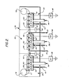
- FIG. 26 a diagrammatic representation of a multiple chamber glow discharge chamber deposition apparatus for the continuous production of photovoltaic cells is generally illustrated by the reference numeral 26.
- the apparatus 26 includes a plurality of isolated, dedicated deposition chambers, each chamber of which is interconnected by a gas gate 42 through which sweep gases and a web of substrate material 11 are adapted to unidirectionally pass.
- the apparatus 26 is adapted to mass produce, in the preferred embodiment, large area, amorphous photovoltaic cells having a p-i-n type configuration on the deposition surface of the substrate material 11 which is continually fed therethrough.
- the apparatus 26 includes at least one triad of deposition chambers 28, 30 and 32.
- Each triad of deposition chamber comprises: a first deposition chamber 28 in which a p-type conductivity amorphous alloy layer is deposited onto the deposition surface of the substrate 11 as the substrate 11 passes therethrough; a second deposition chamber 30 in which an intrinsic amorphous alloy layer is deposited atop the p-type alloy layer on the deposition surface of the substrate 11 as the substrate 11 passes therethrough; and a third deposition chamber 32 in which an n-type conductivity alloy layer is deposited atop the intrinsic layer on the deposition surface of the substrate 11 as the substrate 11 passes therethrough.
- the cathode shields of the present invention are applicable to any type of glow discharge deposition apparatus, whether continuous process or batch-process prepared; (3) a substrate supply core lla and a substrate take-up core llb are shown in the deposition chambers 28 and 32, respectively, for illustrative purposes only, while in reality the cores lla and lIb would be housed in separate chambers operatively connected to the deposition chambers; and (4) although the glow discharge illustrated herein employs cathodes with r.f. power, other glow discharge techniques, such as cathodes with microwave frequencies, may be employed without departing from the spirit of the present invention.
- each deposition chamber 28, 30 and 32 of the triad is adapted to deposit a single semiconductor alloy layer by glow discharge deposition onto the substrate 11.
- each of the deposition chambers 28, 30 and 32 includes: a cathode 34; a shield 35 disposed about each of the cathodes 34; a process gas supply conduit 36 for introducing process gas mixtures into the area adjacent the cathodes; an inert sweep gas conduit 37 disposed on opposite sides of the intrinsic deposition chamber; a radio frequency generator 38; an evacuation conduit 41 for removing unused process gases and nondeposited plasma; a plurality of transversely extending magnetic elements 50; a plurality of radiant heating elements shown schematically as 40; and a gas gate 42 operatively connecting the intrinsic deposition chamber 30 to each of the dopant chambers 28 and 32.
- the supply conduits 36 are operatively associated with the respective cathodes 34 to deliver process gas mixtures to the plasma regions created in each deposition chamber between said cathodes 34 and the substrate 11.
- the cathode shields 35 are adapted to operate in conjunction with the web of substrate material 11 and the evacuation conduit 41 to substantially confine the plasma within the cathode region of the deposition chambers.
- the radio frequency generators 38 operate in conjunction with the cathodes 34, the radiant heaters 40 and the grounded substrate 11 to form the plasma by disassociating the elemental process gases entering the deposition chambers into deposition species.
- the deposition species are then deposited onto the bottom surface of the substrate 11 as amorphous semiconductor layers.
- the substrate 11 is maintained substantially flat by the plurality of rows of magnetic elements 50 which provide an attractive force urging the substrate upwardly, out of its normal sagging path of travel.
- a p-type amorphous silicon semiconductor layer 16a is deposited onto the substrate 11 in the deposition chamber 28, an intrinsic amorphous silicon alloy semiconductor layer 18a is deposited atop the p-type layer 16a in the deposition chamber 30 and an n-type amorphous silicon semiconductor alloy layer 20a is deposited atop the intrinsic layer 18a in the deposition chamber 32.
- each of the semiconductor alloy layers 16a, 18a, 20a, and particularly the intrinsic layer 18a, deposited onto a surface of the magnetic substrate 11 be of high purity in order to produce high efficiency photovoltaic devices 10. It is therefore necessary to substantially prevent nonhomogeneous deposition species produced by nonuniform electrodynamic fields adjacent the ends of the cathode 34 from being deposited onto the substrate 11 and forming a semiconductor film differing in homogeneity from the film produced and deposited onto the substrate 11 adjacent the central portion of the cathode 34.
- Figures 4 and 5 illustrate the apparatus of the present invention, which apparatus is adapted to prevent nonhomogeneous semiconductor films produced by nonuniform electrodynamic fields B from being deposited onto the surface of the substrate 11.
- the apparatus includes a pair of substantially identical shielding plates 60, each of which is positioned adjacent one of the opposed ends of each of the at least one cathode 34 in each deposition chamber. It should be apparent that, although only a single cathode is shown in the schematic drawing of the deposition chambers of Figure 2, a plurality of cathodes may actually be used in a single deposition chamber. In such instances, a shielding plate 60 is to be positioned adjacent each end of each cathode.
- the shielding plates 60 are thin, elongated metallic, nonmagnetic members, preferably of 304 stainless steel. In the preferred embodiment, each plate 60 is approximately 5 cm wide and approximately 35 cm long. The length of the shielding plate 60 is selected so as to substantially cover the transverse width of the substrate 11 being employed. The width of the shielding plate 60 is selected so that the plate will both overlap the edge of the cathode 34 and blanket the portion of the substrate 11 extending immediately adjacent and longitudinally removed from the edge of the cathode (preferably referred to as the region of nonuniform electrodynamic fields B illustrated in Fig. 4). The length of the shielding plates 60 is readily modifiable to accommodate substrates of various widths.
- the width of the shielding plates 60 is readily modifiable if it were determined that the nonuniform electrodynamic fields B extended beyond and were causing nonhomogeneous films to be deposited outside of the region blanketed by the current approximate 5 cm width of the plates.
- Figure 4 illustrates the manner in which the shielding plates 60 blanket the substrate 11 in the areas of nonuniform electrodynamic fields B so that plasma developed by fields B is deposited onto the shielding plates 60 rather than onto the substrate 11 which travels past shielding plates 60 in the direction of arrow 9.
- the shielding plates 60 are positioned in a plane generally parallel to the plane of travel of the substrate 11 but removed downwardly therefrom by a distance of approximately 6 to 7 mm.
- a polymer such as a polyimide, film 61, as illustrated in Fig. 5, is placed onto at least the surface of the shielding plates 60 facing the substrate.
- the polyimide film 61 both prevents discharge in the area between the substrate 11 and the plates 60 and prevents deposition onto the upper surface of the shielding plates 60.
- the polyimide film may be KAPTON (registered trademark of Dupont Corporation), type 4. Polyimide films were selected because of their inherent properties of high temperature stability, good wear resistance at high temperature and low out- gassing in high vacuum. While other films may be used, they should exhibit similar properties.
- Figure 5 depicts the operative deployment of the shielding plates 60 in a deposition chamber such as a dopant chamber 28.
- the deposition chamber 28 includes a left hand plasma confining shield 35 which includes a top flange 35a, side wall 35b, and a front wall 35c.
- the bottom surface of the substrate 11 contacts the upper surface of flange 35a to substantially prevent process gases and plasma from leaking out of the plasma region.
- a similar plasma confining shield (although not shown) is positioned on the right hand side of the deposition chamber 28 so that the right and left hand shields in combination with the lower wall of the chamber and the bottom surface of the substrate substantially confine the plasma to the cathode region of the deposition chamber 28.
- the substrate shielding plates 60 are formed with angled spacing flanges 60b and mounting flanges 60a.
- the mounting flanges 60a are employed to connect the shielding plates 60 to the top flanges 35a of the plasma confinement shields 35.
- the spacing flanges 60b serve to space the shielding plates 60 from the layered surface of the substrate 11 the preferred approximately 6.5 mm distance.
- the substrate shielding plates 60 substantially prevent diassociated species formed by nonuniform electrodynamic fields B from reaching and being deposited onto the substrate 11.
- the result is the deposition onto the web of substrate material 11 of homogeneous semiconductor layers produced by uniform electrodynamic fields A formed in the central cathode region. This, of course, assumes the absence of material nonuniformities in the direction of substrate movement 9.
Abstract
Description
- This invention relates generally to apparatus for producing improved photovoltaic devices and more particularly to substrate shields for substantially reducing the glow discharge deposition of nonhomogeneous semiconductor films onto a substrate, the nonhomogeneous nature of the films caused by nonuniform electrodynamic fields developed at the ends of the cathodes.
- This invention relates to apparatus for continuously producing photovoltaic devices on a substrate by depositing successive semiconductor layers in each of at least two adjacent glow discharge deposition chambers. The composition of each semiconductor layer is dependent upon, among other things, the particular process gases introduced into each of the deposition chambers and the method of forming the semiconductor layer from those process gases. More particularly, the process gases introduced into the first deposition chamber are carefully controlled and isolated from the gases introduced into the adjacent deposition chamber to provide semiconductor layers of very high quality. If all semiconductor layers are not of high quality, the overall efficiency of the semiconductor device produced from those layers suffers. It is therefore necessary to carefully monitor all steps and materials which directly affect the quality of the semiconductor layers produced.
- In the glow discharge deposition of semiconductor films onto a substrate, process gases introduced into the dedicated deposition chambers are directed to flow between a cathode and the substrate. Within the plasma region, the area bounded by the cathode and substrate, the power that is supplied to the cathode causes the formation of an electrodynamic field in the plasma region which operates to disassociate the process gases into species which are then deposited onto the substrate. If the electrodynamic field is not uniform over the entire length of the cathode, the properties of the semiconductor films deposited onto the substrate will be affected accordingly. More particularly, nonuniform areas in the electrodynamic field created between the cathode and substrate result in the deposition of nonhomogeneous semiconductor layers. It is therefore a principle purpose of the present invention to substantially prevent nonhomogeneous semiconductor layers formed by nonuniform electrodynamic fields from being deposited onto the substrate.
- Recently, considerable efforts have been made to develop systems for depositing amorphous semiconductor alloys which can encompass relatively large areas, and which can be doped to form p-type and n-type materials for the production of p-i-n type devices which are, in operation, substantially equivalent to their crystalline counterparts.
- It is now possible to prepare amorphous silicon alloys by glow discharge techniques which possess: (1) acceptable concentrations of localized states in the energy gaps thereof; and (2) high quality electronic properties. Such a technique is fully described in U.S. Patent No. 4,226,898, entitled Amorphous Semiconductors Equivalent to Crystalline Semiconductors, issued October 7, 1980 to Stanford R. Ovshinsky and Arun Madan; and by vapor deposition as fully described in U.S. Patent No. 4,217,374, which issued on August 12, 1980 to Stanford R. Ovshinsky and Masatsugu Izu under the same title. As disclosed in these patents, fluorine introduced into the amorphous silicon semiconductor layers operates to substantially reduce the density of the localized states therein and facilitates the addition of other alloying materials, such as germanium.
- The concept of utilizing multiple cells, to enhance photovoltaic device efficiency, was discussed at least as early as 1955 by E.D. Jackson in U.S. Patent No. 2,949,498 issued August 16, 1960. The multiple cell structures therein discussed utilized p-n junction crystalline semiconductor devices. Essentially the concept is directed to utilizing different band gap devices to more efficiently collect various portions of the solar spectrum and to increase open circuit voltage (Voc.). The tandem cell device has two or more cells with the light being directed serially through each cell, with a large band gap material followed by smaller band gap materials to absorb the light passed through the first cell. By substantially matching the generated currents from each cell, the overall open circuit voltages from each cell may be added, thereby making the greatest use of the light energy passing through the semiconductor device.
- It is of obvious commercial importance to be able to mass produce amorphous photovoltaic devices. Unlike crystalline silicon, which is limited to batch processing for the manufacture of solar cells, amorphous silicon alloys can be deposited in multiple layers over large area substrates to form solar cells in a high volume, continuous processing system. In continuous processing systems of this kind, a substrate may be continuously advanced through a succession of deposition chambers, wherein each chamber is dedicated to the deposition of a specific material. In making a solar cell of'p-i-n type configuration, the first chamber is dedicated for depositing a p-type amorphous silicon alloy, the second chamber is dedicated for depositing an intrinsic amorphous silicon alloy, and the third chamber is dedicated for depositing an n-type amorphous silicon alloy. Since each deposited alloy, and especially the intrinsic alloy, must be of high purity, the deposition environment in the intrinsic deposition chamber is isolated from the doping constituents within the other chambers to prevent the back diffusion of doping constituents into the intrinsic chamber. In the previously mentioned systems which are primarily concerned with the production of photovoltaic cells, isolation between the chambers is accomplished by gas gates through which unidirectional gas flow is established and through which an inert gas may be "swept" about the web of substrate material.
- Recent improvements in continuous glow discharge deposition apparatus such as: (1) establishing a substantially unidirectional flow of gases from the intrinsic deposition chamber to adjacent dopant chambers through a small gas gate passageway; (2) reducing the size of those passageways by employing magnetic assemblies which urge the unlayered substrate surface toward one of the passageway walls; and (3) using a flow of inert sweep gases across the gas gate passageway, have substantially improved the quality of semiconductor layers produced from the deposition apparatus. However, any aspect of manufacturing which adversely affects the quality of films produced cannot be tolerated. Accordingly, it has been discovered that the homogeneity of a semiconductor layer deposited onto the substrate at the portions of the plasma region proximate the ends of the cathodes varies from the homogeneity of the semiconductor layer deposited onto the substrate at the portions of the plasma region medial to those end portions of the cathodes.
- By way of illustration, and referring to the drawing of Figure 3,
arrow 9 indicates the direction of movement ofgrounded substrate 11 which is spaced abovecathode 34 to define aplasma region 80 therebetween wherein process gases are disassociated into elemental forms. In theplasma region 80, two different electrodynamic fields are present. Depending upon the nature of the electrodynamic field, the reaction kinetics for the plasma discharge will vary. Accordingly, the properties of the semiconductor layer deposited in the electrodynamic field labelled "A" are different from the properties of the semiconductor layer deposited in the electrodynamic fields labelled "B". It should therefore be readily apparent that such nonuniform electrodynamic fields in theplasma region 80 cause serious problems to deposition apparatus which utilizes a continuously moving substrate. - Still referring to Figure 3, the electrodynamic field A is substantially uniform in the direction of
substrate movement 9, whereas the electrodynamic fields B are substantially nonuniform. This difference in uniformity of fields is due to the fact that field A is developed in a portion of the plasma region in which the distance between the substrate and the cathode is constant, thereby promoting field lines substantially perpendicular to the plane of the substrate, while fields B are developed in portions of theplasma region 80 adjacent the ends of thecathode 34 in which the substrate-cathode distance varies, thereby promoting angled or bent field lines relative to the plane of the substrate. The result of a substrate traveling through a plasma region characterized by nonuniform electrodynamic fields is the deposition on the substrate of a nonhomogeneous semiconductor layer. - It is therefore the principle object of the present invention to substantially prevent the plasma formed in the presence of nonuniform fields formed adjacent the edges of the cathodes from being deposited onto the surface of the substrate as the substrate continuously moves past the cathodes.
- Disclosed herein are a pair of substrate shields adapted to cooperate with a cathode to substantially prevent nonhomogeneous semiconductor films formed in the portion of the plasma region wherein the electrodynamic lines of force are not substantially perpendicular to the substrate from being deposited onto the substrate, so that the semiconductor layer deposited onto the substrate is homogeneous. The deposition apparatus is preferably the type which includes at least two isolated glow discharge deposition chambers operatively connected by a gas gate passageway which is adapted to channel a unidirectional flow of inert sweep gases from one to the adjacent chamber of each pair of deposition chambers, and through which a web of substrate material continuously travels. Each deposition chamber includes at least one elongated cathode connected to, preferably, an R.F. power source for energization of the cathode and disassociation of process gases introduced in the region between the cathode and the substrate into elemental forms for deposition onto the substrate. The electrodynamic fields created adjacent the ends of the elongated, substantially planar cathode produce a semiconductor film different than the semiconductor film produced by the relatively large electrodynamic field created at the central portion of the cathode. The substrate shields of the present invention are elongated, substantially planar plates which extend across the transverse width of the deposition chamber so as to collect the plasma produced in the presence of those end-effected electrodynamic fields. In this manner, only the plasma produced in the uniform, central electrodynamic field may be deposited onto the substrate. The result is the deposition of a substantially homogeneous semiconductor layer. The shields are preferably coated with a polymer, such as a polyimide, film to prevent discharges in the newly defined region between the shield and the substrate.
- These and other objects and advantages of the present invention will become clear from the drawings, the claims and the detailed description of the invention which follow.
- Accordingly, a first object of the invention is to provide a glow discharge deposition apparatus wherein semiconductor layers are deposited w onto a substrate, the deposition apparatus having at least one dedicated deposition chamber which includes a substrate, at least one cathode spaced from the substrate, means for introducing process gases between the substrate and the cathode and means for energizing the at least one cathode to develop an electrodynamic field in which the process gases are disassociated into plasma, the field having a central substantially uniform region separating a pair of nonuniform regions. The improvement is characterized by means adapted to substantially prevent nonhomogeneous semiconductor films formed by the nonuniform electrodynamic fields from being deposited onto the substrate, such that only the substantially homogeneous semiconductor film formed by the central uniform electrodynamic field is deposited onto the substrate.
-
- Figure 1 is a fragmentary, cross-sectional view of a tandem photovoltaic device comprising a plurality of p-i-n type cells, each layer of the cells formed from a semiconductor alloy;
- Figure 2 is a diagrammatic representation of a multiple glow discharge chamber deposition system adapted for use in the continuous production of photovoltaic devices such as the cells shown in Figure 1;
- Figure 3 is an enlarged, schematic representation of the nonuniform electrodynamic fields developed in the plasma region of a glow discharge deposition chamber not equipped with the shields of the present invention;
- Figure 4 is an enlarged, schematic representation illustrating the manner in which the shields of the present invention are positioned to substantially prevent nonhomogeneous plasma produced in regions of nonuniform electrodynamic fields from being deposited onto the substrate; and
- Figure 5 is an enlarged, fragmentary perspective view illustrating the substrate shields of the present invention operatively disposed within a glow discharge deposition chamber.
- Referring now to the drawings and particularly to Figure 1, a photovoltaic cell formed of a plurality of successive p-i-n layers, each of which includes, in the preferred embodiment, an amorphous semiconductor alloy, is shown generally by the
numeral 10. It is for the production of this type of photovoltaic device, wherein homogeneous amorphous alloy layers are continuously deposited onto a substrate in successive isolated deposition chambers, that the substrate shields of the present invention were developed. - More,particularly, Figure 1 shows a p-i-n type
photovoltaic device 10 such as a solar cell made up of individualp-i-n type cells 12a, 12b and 12c. Below the lowermost cell 12a is asubstrate 11 which may be transparent or formed from a metallic material such as stainless steel, aluminum, tantalum, molybdenum or chrome. Although certain applications may require a thin oxide layer and/or a series of base contacts prior to application of the amorphous material, for purposes of this application the term "substrate" shall include not only a flexible film, but also any elements added thereto by preliminary processing. - Each of the
cells 12a, 12b and 12c are fabricated with an amorphous alloy body containing at least a silicon alloy. Each of the alloy bodies includes a p-type conductivity region orlayer layer layer cell 12b is an intermediate cell and, as indicated in Figure 1, additional intermediate cells may be stacked atop the illustrated cells without departing from the spirit or scope of the present invention. Also, although p-i-n cells are illustrated, the substrate shields of this invention may also be used with apparatus adapted to produce single or multiple n-i-p cells. - It is to be understood that following the deposition of the semiconductor alloy layers, a further deposition process may be either performed in a separate environment or as a part of a continuous process. In this step, a TCO (transparent conductive oxide)
layer 22 is added. Anelectrode grid 24 may be added to the device where the cell is of a sufficiently large area, or if the conductivity of theTCO layer 22 is insufficient. Thegrid 24 shortens the carrier path and increases the conduction efficiency. - Turning now to Figure 2, a diagrammatic representation of a multiple chamber glow discharge chamber deposition apparatus for the continuous production of photovoltaic cells is generally illustrated by the
reference numeral 26. Theapparatus 26 includes a plurality of isolated, dedicated deposition chambers, each chamber of which is interconnected by agas gate 42 through which sweep gases and a web ofsubstrate material 11 are adapted to unidirectionally pass. - The
apparatus 26 is adapted to mass produce, in the preferred embodiment, large area, amorphous photovoltaic cells having a p-i-n type configuration on the deposition surface of thesubstrate material 11 which is continually fed therethrough. To deposit the amorphous alloy layers required for producing multiple p-i-n type layer cells, theapparatus 26 includes at least one triad ofdeposition chambers first deposition chamber 28 in which a p-type conductivity amorphous alloy layer is deposited onto the deposition surface of thesubstrate 11 as thesubstrate 11 passes therethrough; asecond deposition chamber 30 in which an intrinsic amorphous alloy layer is deposited atop the p-type alloy layer on the deposition surface of thesubstrate 11 as thesubstrate 11 passes therethrough; and athird deposition chamber 32 in which an n-type conductivity alloy layer is deposited atop the intrinsic layer on the deposition surface of thesubstrate 11 as thesubstrate 11 passes therethrough. It should be apparent that: (1) although only one triad of deposition chambers has been illustrated, additional triads or additional individual chambers may be added to the apparatus to provide the machine with the capability of producing photovoltaic cells having any number of amorphous p-i-n type layers; (2) the cathode shields of the present invention are applicable to any type of glow discharge deposition apparatus, whether continuous process or batch-process prepared; (3) a substrate supply core lla and a substrate take-up core llb are shown in thedeposition chambers - Each
deposition chamber substrate 11. To that end, each of thedeposition chambers cathode 34; ashield 35 disposed about each of thecathodes 34; a processgas supply conduit 36 for introducing process gas mixtures into the area adjacent the cathodes; an inertsweep gas conduit 37 disposed on opposite sides of the intrinsic deposition chamber; aradio frequency generator 38; anevacuation conduit 41 for removing unused process gases and nondeposited plasma; a plurality of transversely extendingmagnetic elements 50; a plurality of radiant heating elements shown schematically as 40; and agas gate 42 operatively connecting theintrinsic deposition chamber 30 to each of thedopant chambers - The
supply conduits 36 are operatively associated with therespective cathodes 34 to deliver process gas mixtures to the plasma regions created in each deposition chamber between saidcathodes 34 and thesubstrate 11. The cathode shields 35 are adapted to operate in conjunction with the web ofsubstrate material 11 and theevacuation conduit 41 to substantially confine the plasma within the cathode region of the deposition chambers. - The
radio frequency generators 38 operate in conjunction with thecathodes 34, theradiant heaters 40 and the groundedsubstrate 11 to form the plasma by disassociating the elemental process gases entering the deposition chambers into deposition species. The deposition species are then deposited onto the bottom surface of thesubstrate 11 as amorphous semiconductor layers. Thesubstrate 11 is maintained substantially flat by the plurality of rows ofmagnetic elements 50 which provide an attractive force urging the substrate upwardly, out of its normal sagging path of travel. - To form the
photovoltaic cell 10 representing the preferred embodiment illustrated in Figure 1, a p-type amorphous silicon semiconductor layer 16a is deposited onto thesubstrate 11 in thedeposition chamber 28, an intrinsic amorphous siliconalloy semiconductor layer 18a is deposited atop the p-type layer 16a in thedeposition chamber 30 and an n-type amorphous silicon semiconductor alloy layer 20a is deposited atop theintrinsic layer 18a in thedeposition chamber 32. - It is important that each of the
semiconductor alloy layers 16a, 18a, 20a, and particularly theintrinsic layer 18a, deposited onto a surface of themagnetic substrate 11 be of high purity in order to produce high efficiencyphotovoltaic devices 10. It is therefore necessary to substantially prevent nonhomogeneous deposition species produced by nonuniform electrodynamic fields adjacent the ends of thecathode 34 from being deposited onto thesubstrate 11 and forming a semiconductor film differing in homogeneity from the film produced and deposited onto thesubstrate 11 adjacent the central portion of thecathode 34. III. The Shielding Plates Of The Present Invention - Figures 4 and 5 illustrate the apparatus of the present invention, which apparatus is adapted to prevent nonhomogeneous semiconductor films produced by nonuniform electrodynamic fields B from being deposited onto the surface of the
substrate 11. - The apparatus includes a pair of substantially
identical shielding plates 60, each of which is positioned adjacent one of the opposed ends of each of the at least onecathode 34 in each deposition chamber. It should be apparent that, although only a single cathode is shown in the schematic drawing of the deposition chambers of Figure 2, a plurality of cathodes may actually be used in a single deposition chamber. In such instances, a shieldingplate 60 is to be positioned adjacent each end of each cathode. - The shielding
plates 60 are thin, elongated metallic, nonmagnetic members, preferably of 304 stainless steel. In the preferred embodiment, eachplate 60 is approximately 5 cm wide and approximately 35 cm long. The length of the shieldingplate 60 is selected so as to substantially cover the transverse width of thesubstrate 11 being employed. The width of the shieldingplate 60 is selected so that the plate will both overlap the edge of thecathode 34 and blanket the portion of thesubstrate 11 extending immediately adjacent and longitudinally removed from the edge of the cathode (preferably referred to as the region of nonuniform electrodynamic fields B illustrated in Fig. 4). The length of the shieldingplates 60 is readily modifiable to accommodate substrates of various widths. Likewise, the width of the shieldingplates 60 is readily modifiable if it were determined that the nonuniform electrodynamic fields B extended beyond and were causing nonhomogeneous films to be deposited outside of the region blanketed by the current approximate 5 cm width of the plates. - Figure 4 illustrates the manner in which the
shielding plates 60 blanket thesubstrate 11 in the areas of nonuniform electrodynamic fields B so that plasma developed by fields B is deposited onto the shieldingplates 60 rather than onto thesubstrate 11 which travels past shieldingplates 60 in the direction ofarrow 9. In order to best accomplish that function, the shieldingplates 60 are positioned in a plane generally parallel to the plane of travel of thesubstrate 11 but removed downwardly therefrom by a distance of approximately 6 to 7 mm. - Finally, a polymer, such as a polyimide,
film 61, as illustrated in Fig. 5, is placed onto at least the surface of the shieldingplates 60 facing the substrate. Thepolyimide film 61 both prevents discharge in the area between thesubstrate 11 and theplates 60 and prevents deposition onto the upper surface of the shieldingplates 60. The polyimide film may be KAPTON (registered trademark of Dupont Corporation), type 4. Polyimide films were selected because of their inherent properties of high temperature stability, good wear resistance at high temperature and low out- gassing in high vacuum. While other films may be used, they should exhibit similar properties. - Figure 5 depicts the operative deployment of the shielding
plates 60 in a deposition chamber such as adopant chamber 28. As depicted therein, thedeposition chamber 28 includes a left handplasma confining shield 35 which includes atop flange 35a,side wall 35b, and afront wall 35c. The bottom surface of thesubstrate 11 contacts the upper surface offlange 35a to substantially prevent process gases and plasma from leaking out of the plasma region. A similar plasma confining shield (although not shown) is positioned on the right hand side of thedeposition chamber 28 so that the right and left hand shields in combination with the lower wall of the chamber and the bottom surface of the substrate substantially confine the plasma to the cathode region of thedeposition chamber 28. Thesubstrate shielding plates 60 are formed withangled spacing flanges 60b and mountingflanges 60a. The mountingflanges 60a are employed to connect theshielding plates 60 to thetop flanges 35a of the plasma confinement shields 35. Thespacing flanges 60b serve to space the shieldingplates 60 from the layered surface of thesubstrate 11 the preferred approximately 6.5 mm distance. - In this manner, the
substrate shielding plates 60 substantially prevent diassociated species formed by nonuniform electrodynamic fields B from reaching and being deposited onto thesubstrate 11. The result is the deposition onto the web ofsubstrate material 11 of homogeneous semiconductor layers produced by uniform electrodynamic fields A formed in the central cathode region. This, of course, assumes the absence of material nonuniformities in the direction ofsubstrate movement 9. - It should be understood that the present invention is not limited to the precise structure of the illustrated embodiments. It is intended that the foregoing description of the presently preferred embodiments be regarded as an illustration rather than as a limitation of the present invention.
Claims (7)
Priority Applications (1)
| Application Number | Priority Date | Filing Date | Title |
|---|---|---|---|
| AT83305309T ATE21126T1 (en) | 1982-09-16 | 1983-09-12 | SUBSTRATE SHIELDING TO PREVENT IRREGULAR DEPOSITION OF A FILM. |
Applications Claiming Priority (2)
| Application Number | Priority Date | Filing Date | Title |
|---|---|---|---|
| US06/418,859 US4574733A (en) | 1982-09-16 | 1982-09-16 | Substrate shield for preventing the deposition of nonhomogeneous films |
| US418859 | 1982-09-16 |
Publications (3)
| Publication Number | Publication Date |
|---|---|
| EP0109148A2 true EP0109148A2 (en) | 1984-05-23 |
| EP0109148A3 EP0109148A3 (en) | 1984-07-18 |
| EP0109148B1 EP0109148B1 (en) | 1986-07-30 |
Family
ID=23659837
Family Applications (1)
| Application Number | Title | Priority Date | Filing Date |
|---|---|---|---|
| EP83305309A Expired EP0109148B1 (en) | 1982-09-16 | 1983-09-12 | Substrate shield for preventing the deposition of nonhomogeneous films |
Country Status (10)
| Country | Link |
|---|---|
| US (1) | US4574733A (en) |
| EP (1) | EP0109148B1 (en) |
| JP (1) | JPS5972722A (en) |
| AT (1) | ATE21126T1 (en) |
| AU (1) | AU558048B2 (en) |
| CA (1) | CA1196604A (en) |
| DE (1) | DE3364966D1 (en) |
| IL (1) | IL69712A (en) |
| IN (1) | IN159575B (en) |
| PH (1) | PH20460A (en) |
Cited By (2)
| Publication number | Priority date | Publication date | Assignee | Title |
|---|---|---|---|---|
| EP0198604A1 (en) * | 1985-03-18 | 1986-10-22 | Energy Conversion Devices, Inc. | Glow discharge deposition apparatus having confined plasma region |
| WO2009059640A1 (en) * | 2007-11-08 | 2009-05-14 | Applied Materials Inc., A Corporation Of The State Of Delaware | Electrode arrangement with movable shield |
Families Citing this family (9)
| Publication number | Priority date | Publication date | Assignee | Title |
|---|---|---|---|---|
| US5122394A (en) * | 1985-12-23 | 1992-06-16 | Atochem North America, Inc. | Apparatus for coating a substrate |
| US4928627A (en) * | 1985-12-23 | 1990-05-29 | Atochem North America, Inc. | Apparatus for coating a substrate |
| FR2606038B1 (en) * | 1986-10-30 | 1988-12-16 | Ibm France | IMPROVEMENT IN SPEAKERS FOR THE TREATMENT OF SEMICONDUCTOR SUBSTRATES |
| JPH0630850Y2 (en) * | 1989-04-25 | 1994-08-17 | 日本真空技術株式会社 | Plasma CVD equipment |
| DE4324320B4 (en) * | 1992-07-24 | 2006-08-31 | Fuji Electric Co., Ltd., Kawasaki | Method and device for producing a thin-film photovoltaic conversion device |
| US5433812A (en) * | 1993-01-19 | 1995-07-18 | International Business Machines Corporation | Apparatus for enhanced inductive coupling to plasmas with reduced sputter contamination |
| US5363802A (en) * | 1994-04-11 | 1994-11-15 | Novalek, Inc. | Gnaw resistant animal watering bottle |
| DE102004029466A1 (en) * | 2004-06-18 | 2006-01-05 | Leybold Optics Gmbh | Medieninjektor |
| CN112536008A (en) * | 2019-09-20 | 2021-03-23 | 中国石油化工股份有限公司 | Plasma reactor and online decoking method thereof |
Citations (6)
| Publication number | Priority date | Publication date | Assignee | Title |
|---|---|---|---|---|
| US3485666A (en) * | 1964-05-08 | 1969-12-23 | Int Standard Electric Corp | Method of forming a silicon nitride coating |
| FR2208005A1 (en) * | 1972-11-29 | 1974-06-21 | Triplex Safety Glass Co | |
| FR2208185A1 (en) * | 1972-11-23 | 1974-06-21 | Balzers Patent Beteilig Ag | |
| FR2280972A1 (en) * | 1974-08-02 | 1976-02-27 | Lfe Corp | APPARATUS FOR REACTING A GAS WITH A MATERIAL |
| FR2339001A1 (en) * | 1976-01-22 | 1977-08-19 | Western Electric Co | RADIAL FLOW REACTOR FOR COATING FORMATION |
| EP0041773A1 (en) * | 1980-05-19 | 1981-12-16 | Energy Conversion Devices, Inc. | Solar cell production |
Family Cites Families (4)
| Publication number | Priority date | Publication date | Assignee | Title |
|---|---|---|---|---|
| FR2265872B1 (en) * | 1974-03-27 | 1977-10-14 | Anvar | |
| US4317844A (en) * | 1975-07-28 | 1982-03-02 | Rca Corporation | Semiconductor device having a body of amorphous silicon and method of making the same |
| JPS5681922A (en) * | 1979-12-06 | 1981-07-04 | Sumitomo Electric Ind Ltd | Manufacture of thin film |
| US4369730A (en) * | 1981-03-16 | 1983-01-25 | Energy Conversion Devices, Inc. | Cathode for generating a plasma |
-
1982
- 1982-09-16 US US06/418,859 patent/US4574733A/en not_active Expired - Lifetime
-
1983
- 1983-09-06 IN IN1085/CAL/83A patent/IN159575B/en unknown
- 1983-09-09 AU AU18978/83A patent/AU558048B2/en not_active Ceased
- 1983-09-12 DE DE8383305309T patent/DE3364966D1/en not_active Expired
- 1983-09-12 AT AT83305309T patent/ATE21126T1/en not_active IP Right Cessation
- 1983-09-12 JP JP58168083A patent/JPS5972722A/en active Granted
- 1983-09-12 EP EP83305309A patent/EP0109148B1/en not_active Expired
- 1983-09-13 IL IL69712A patent/IL69712A/en unknown
- 1983-09-13 PH PH29531A patent/PH20460A/en unknown
- 1983-09-16 CA CA000436881A patent/CA1196604A/en not_active Expired
Patent Citations (6)
| Publication number | Priority date | Publication date | Assignee | Title |
|---|---|---|---|---|
| US3485666A (en) * | 1964-05-08 | 1969-12-23 | Int Standard Electric Corp | Method of forming a silicon nitride coating |
| FR2208185A1 (en) * | 1972-11-23 | 1974-06-21 | Balzers Patent Beteilig Ag | |
| FR2208005A1 (en) * | 1972-11-29 | 1974-06-21 | Triplex Safety Glass Co | |
| FR2280972A1 (en) * | 1974-08-02 | 1976-02-27 | Lfe Corp | APPARATUS FOR REACTING A GAS WITH A MATERIAL |
| FR2339001A1 (en) * | 1976-01-22 | 1977-08-19 | Western Electric Co | RADIAL FLOW REACTOR FOR COATING FORMATION |
| EP0041773A1 (en) * | 1980-05-19 | 1981-12-16 | Energy Conversion Devices, Inc. | Solar cell production |
Non-Patent Citations (1)
| Title |
|---|
| APPLIED PHYSICS LETTERS, vol. 32, no. 4, February 1978, pages 245,246 * |
Cited By (4)
| Publication number | Priority date | Publication date | Assignee | Title |
|---|---|---|---|---|
| EP0198604A1 (en) * | 1985-03-18 | 1986-10-22 | Energy Conversion Devices, Inc. | Glow discharge deposition apparatus having confined plasma region |
| JPS61264179A (en) * | 1985-03-18 | 1986-11-22 | エナージー・コンバーション・デバイセス・インコーポレーテッド | Glow discharge deposition apparatus having plasma confining region |
| WO2009059640A1 (en) * | 2007-11-08 | 2009-05-14 | Applied Materials Inc., A Corporation Of The State Of Delaware | Electrode arrangement with movable shield |
| US8398775B2 (en) | 2007-11-08 | 2013-03-19 | Applied Materials, Inc. | Electrode and arrangement with movable shield |
Also Published As
| Publication number | Publication date |
|---|---|
| CA1196604A (en) | 1985-11-12 |
| US4574733A (en) | 1986-03-11 |
| DE3364966D1 (en) | 1986-09-04 |
| JPS5972722A (en) | 1984-04-24 |
| AU558048B2 (en) | 1987-01-15 |
| ATE21126T1 (en) | 1986-08-15 |
| JPH0576171B2 (en) | 1993-10-22 |
| AU1897883A (en) | 1984-03-22 |
| IL69712A0 (en) | 1983-12-30 |
| EP0109148B1 (en) | 1986-07-30 |
| IL69712A (en) | 1986-12-31 |
| EP0109148A3 (en) | 1984-07-18 |
| PH20460A (en) | 1987-01-14 |
| IN159575B (en) | 1987-05-30 |
Similar Documents
| Publication | Publication Date | Title |
|---|---|---|
| EP0109808B1 (en) | An improved apparatus for the manufacture of photovoltaic devices | |
| US4678679A (en) | Continuous deposition of activated process gases | |
| US4537795A (en) | Method for introducing sweep gases into a glow discharge deposition apparatus | |
| US4462333A (en) | Process gas introduction, confinement and evacuation system for glow discharge deposition apparatus | |
| US4480585A (en) | External isolation module | |
| EP0099708B1 (en) | Magnetic apparatus for reducing substrate warpage | |
| EP0109148B1 (en) | Substrate shield for preventing the deposition of nonhomogeneous films | |
| CA1206244A (en) | Process gas introduction and channeling system | |
| US4520757A (en) | Process gas introduction, confinement and evacuation system for glow discharge deposition apparatus | |
| US4513684A (en) | Upstream cathode assembly | |
| US4608943A (en) | Cathode assembly with localized profiling capabilities | |
| CA1248210A (en) | Upstream cathode assembly | |
| EP0591398B1 (en) | Chemically active isolation passageway for deposition chambers | |
| US4626447A (en) | Plasma confining apparatus | |
| EP0100611B1 (en) | Reduced capacitance electrode assembly | |
| EP0106521B1 (en) | Baffle system for glow discharge deposition apparatus | |
| US20040250763A1 (en) | Fountain cathode for large area plasma deposition |
Legal Events
| Date | Code | Title | Description |
|---|---|---|---|
| PUAI | Public reference made under article 153(3) epc to a published international application that has entered the european phase |
Free format text: ORIGINAL CODE: 0009012 |
|
| PUAL | Search report despatched |
Free format text: ORIGINAL CODE: 0009013 |
|
| AK | Designated contracting states |
Designated state(s): AT BE CH DE FR GB IT LI LU NL SE |
|
| AK | Designated contracting states |
Designated state(s): AT BE CH DE FR GB IT LI LU NL SE |
|
| 17P | Request for examination filed |
Effective date: 19841108 |
|
| GRAA | (expected) grant |
Free format text: ORIGINAL CODE: 0009210 |
|
| AK | Designated contracting states |
Kind code of ref document: B1 Designated state(s): AT BE CH DE FR GB IT LI LU NL SE |
|
| PG25 | Lapsed in a contracting state [announced via postgrant information from national office to epo] |
Ref country code: BE Effective date: 19860730 Ref country code: AT Effective date: 19860730 |
|
| REF | Corresponds to: |
Ref document number: 21126 Country of ref document: AT Date of ref document: 19860815 Kind code of ref document: T |
|
| PG25 | Lapsed in a contracting state [announced via postgrant information from national office to epo] |
Ref country code: SE Effective date: 19860731 |
|
| ITF | It: translation for a ep patent filed |
Owner name: ING. C. GREGORJ S.P.A. |
|
| REF | Corresponds to: |
Ref document number: 3364966 Country of ref document: DE Date of ref document: 19860904 |
|
| ET | Fr: translation filed | ||
| PG25 | Lapsed in a contracting state [announced via postgrant information from national office to epo] |
Ref country code: LU Free format text: LAPSE BECAUSE OF NON-PAYMENT OF DUE FEES Effective date: 19860930 |
|
| PGFP | Annual fee paid to national office [announced via postgrant information from national office to epo] |
Ref country code: NL Payment date: 19860930 Year of fee payment: 4 |
|
| PLBE | No opposition filed within time limit |
Free format text: ORIGINAL CODE: 0009261 |
|
| STAA | Information on the status of an ep patent application or granted ep patent |
Free format text: STATUS: NO OPPOSITION FILED WITHIN TIME LIMIT |
|
| 26N | No opposition filed | ||
| PG25 | Lapsed in a contracting state [announced via postgrant information from national office to epo] |
Ref country code: LI Effective date: 19870930 Ref country code: CH Effective date: 19870930 |
|
| PG25 | Lapsed in a contracting state [announced via postgrant information from national office to epo] |
Ref country code: NL Effective date: 19880401 |
|
| NLV4 | Nl: lapsed or anulled due to non-payment of the annual fee | ||
| REG | Reference to a national code |
Ref country code: CH Ref legal event code: PL |
|
| PG25 | Lapsed in a contracting state [announced via postgrant information from national office to epo] |
Ref country code: GB Effective date: 19880912 |
|
| REG | Reference to a national code |
Ref country code: GB Ref legal event code: PCNP |
|
| PG25 | Lapsed in a contracting state [announced via postgrant information from national office to epo] |
Ref country code: FR Free format text: LAPSE BECAUSE OF NON-PAYMENT OF DUE FEES Effective date: 19890531 |
|
| GBPC | Gb: european patent ceased through non-payment of renewal fee | ||
| REG | Reference to a national code |
Ref country code: FR Ref legal event code: ST |
|
| PG25 | Lapsed in a contracting state [announced via postgrant information from national office to epo] |
Ref country code: DE Effective date: 19900601 |