US4364074A - V-MOS Device with self-aligned multiple electrodes - Google Patents
V-MOS Device with self-aligned multiple electrodes Download PDFInfo
- Publication number
- US4364074A US4364074A US06/158,668 US15866880A US4364074A US 4364074 A US4364074 A US 4364074A US 15866880 A US15866880 A US 15866880A US 4364074 A US4364074 A US 4364074A
- Authority
- US
- United States
- Prior art keywords
- recess
- substrate
- self
- conductive layer
- layer
- Prior art date
- Legal status (The legal status is an assumption and is not a legal conclusion. Google has not performed a legal analysis and makes no representation as to the accuracy of the status listed.)
- Expired - Lifetime
Links
Images
Classifications
-
- H—ELECTRICITY
- H10—SEMICONDUCTOR DEVICES; ELECTRIC SOLID-STATE DEVICES NOT OTHERWISE PROVIDED FOR
- H10D—INORGANIC ELECTRIC SEMICONDUCTOR DEVICES
- H10D30/00—Field-effect transistors [FET]
- H10D30/60—Insulated-gate field-effect transistors [IGFET]
- H10D30/63—Vertical IGFETs
-
- H—ELECTRICITY
- H10—SEMICONDUCTOR DEVICES; ELECTRIC SOLID-STATE DEVICES NOT OTHERWISE PROVIDED FOR
- H10B—ELECTRONIC MEMORY DEVICES
- H10B12/00—Dynamic random access memory [DRAM] devices
- H10B12/30—DRAM devices comprising one-transistor - one-capacitor [1T-1C] memory cells
- H10B12/39—DRAM devices comprising one-transistor - one-capacitor [1T-1C] memory cells the capacitor and the transistor being in a same trench
- H10B12/395—DRAM devices comprising one-transistor - one-capacitor [1T-1C] memory cells the capacitor and the transistor being in a same trench the transistor being vertical
-
- H—ELECTRICITY
- H10—SEMICONDUCTOR DEVICES; ELECTRIC SOLID-STATE DEVICES NOT OTHERWISE PROVIDED FOR
- H10W—GENERIC PACKAGES, INTERCONNECTIONS, CONNECTORS OR OTHER CONSTRUCTIONAL DETAILS OF DEVICES COVERED BY CLASS H10
- H10W20/00—Interconnections in chips, wafers or substrates
- H10W20/01—Manufacture or treatment
- H10W20/031—Manufacture or treatment of conductive parts of the interconnections
- H10W20/056—Manufacture or treatment of conductive parts of the interconnections by filling conductive material into holes, grooves or trenches
Definitions
- This invention relates to semiconductor devices, and more particularly to device structures and methods for providing self-aligned contacts for semiconductor devices having vertical structural features such as V-groove metal oxide semiconductor (V-MOS) devices.
- V-MOS V-groove metal oxide semiconductor
- Semiconductor processing techniques which reduce the number of processing steps and/or their complexity are also useful to lower the cost of semiconductor devices by increasing product yield or by increasing density, when the number of critical mask alignment steps can be reduced.
- manufacturing processes which provide a high degree of self-aligning elements, i.e., process steps which do not require the alignment and associated alignment tolerances of photolithographic masks, can indirectly aid in the reduction of the cost of semiconductor devices.
- VMOS ROM by T. J. Rodgers et al, IEEE J. Solid-State Circuits, vol. SC-11, No. 5, October 1976, pp. 614-622, teaches a self-aligning diffusion technique at page 619 for ensuring diffused bit line conductivity around a V-grooved etched MOSFET. A single masking oxide layer is used for the diffusion and V-etch mask.
- U.S. Pat. No. 4,116,720 to Vinson uses a similar technique to define both a V-groove and a buried ion-implanted storage node for a dynamic memory cell.
- U.S. Pat. No. 4,003,036 to Jenne describes a VMOS single FET/capacitor memory cell of the type to which the preferred embodiment of the invention described here has been applied.
- a more specific object is to provide improvements in self-aligned electrodes for use in V-MOS devices, particularly dynamic memory cells.
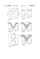
- FIGS. 1-12 are plan and sectional views of a semiconductor substrate at various stages of processing in accordance with the invention to form a single FET-capacitor memory cell in which the gate, source/drain regions and contact metallurgy are formed by self-aligning processing techniques.
- FIGS. 1 and 2 there is shown a partially processed VMOS memory device, generally as taught in U.S. Pat. No. 4,003,036 to Jenne, in which there is provided a P+ semiconductor substrate 10, for example, silicon, including a buried N+ region 12 and an P-type epitaxial semiconductor layer 14. Buried region 12 will subsequently act as a charge storage node for the single FET-capacitor memory cell to be formed in the semiconductor substrate.
- epitaxial layer 14 may include gradations of p-type impurity concentration in order to control the capacitive characteristics of region 12 and/or to control the conduction characteristics of the MOSFET to be subsequently formed.
- a masking layer 16 is provided.
- Masking layer 16 is about 5000-6000 angstroms in thickness so that it can act as a field oxide for devices to be formed.
- photolithographic masking and etching techniques a number of square holes are formed in layer 16. Although only a single hole is shown, it will be understood that an array or matrix of holes are required to form a plurality of memory cells. The exact spacing between holes in layer 16 depends on a number of factors including minimum permissible line widths allowable in the particular process technology in which the semiconductor devices are being implemented.
- an anisotropic etchant such as a hydrazine-water solution is used to etch self-terminating V-shaped pits 18.
- anisotropic etchant such as a hydrazine-water solution is used to etch self-terminating V-shaped pits 18.
- anisotropic etching will provide pyramidal-shaped etch pits limited at the side-walls by 111 surfaces.
- Reference to the article "Optimization of the Hydrazine-Water Solution for Anisotropic Etching of Silicon in Integrated Circuit Technology," M. J. Declercq et al J. Electro-Chem. Soc., April 1975, pages 545-552, will provide more detailed information on anisotropic etching of silicon.
- etch pit 18 Since it is desirable for etch pit 18 to intersect buried region 12, the thickness of layer 14 and the size of the holes in layer 16 require a predetermined relationship. Following the etching of pits 18 a dip etch may be used to remove portions of layer 16 which may extend beyond the top edges of etch pit 18.
- a dielectric layer 20 suitable for a gate oxide for example silicon dioxide of about 500 angstroms may be grown or deposited on the exposed silicon surfaces of etch pit 18.
- a layer of conductive material 22 suitable for a gate electrode is blanket deposited over the dielectric layers 16 and 20.
- the thickness of layer 22 will depend upon the particular material used which may be a silicide, such as tungsten silicide, polysilicon or a refractory metal, such as molybdenum.
- a passivating layer 24 is provided, which is preferred to be a phosphorous doped oxide because of its ability to flow under heat treatment. See U.S. Pat. No. 3,825,442 to Moore for examples of suitable materials.
- a self-leveling photoresist layer is provided over layer 24 and a self-aligned photoresist mask is formed as taught in U.S. patent application Ser. No. 103,981 to R. R. Garnache et al filed Dec. 17, 1979. Briefly, this process includes the steps of depositing a layer of masking material over the substrate which completely fills etch pit 18 and provides a planar upper surface. A controllable directional etching technique is then used to uniformly remove the top portion of the photoresist layer until a self-aligned plug 26 remains in etch pit 18. The amount of photoresist retained in pit 18 should have its upper surface sufficiently below the original top surface of layer 14 to enable the formation of a source or drain region and its associated contact to be formed, as described below, on the side walls of etch pit 18.
- photoresist plug 26 After formation of photoresist plug 26 a second photoresist masking layer is deposited, exposed and developed to protect those portions of layers 22 and 24 which will be used to form the gate electrodes subsequently to become the word access lines in the memory array to be provided.
- second photoresist layer 28 overlying a portion of layer 24 and plug 26.
- the positioning of the mask for defining photoresist layer 28 is not critical as long as a portion overlaps both sides of photoresist plug 26, as shown in FIGS. 5 and 6.
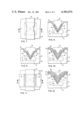
- conductive layer 22 is formed from a molybdenum, silicide or other conductive material not readily oxidizable or self-passivating.
- the substrate is subjected to a heating step, as taught in the above identified patent of Moore, to cause phosphorous doped oxide layer 24 to flow over the exposed edges of conductive layer 22.
- polysilicon may be used as layer 22 and the above steps of providing an overhang and heating can be substituted by an oxidation step provided that a process is used which will enable the growth of a significant thickness of passivating oxide on layer 22 while not significantly increasing the thickness of exposed gate oxide 20. See, for example, the process described in the article, "Low Temperature Oxidation Method for Self-Passivating of Polysilicon Conductors During Gate Oxide Growth," R. Silverman et al, IBM Technical Disclosure Bulletin, August 1979, page 935.
- regions 30 and 32 are formed using both the passivated gate electrode 22 and thick oxide 16 as a mask.
- a preferred technique is to strip exposed portions of gate oxide layer 20 from the top edges of etch pit 18 either prior to or after ion implanting n-type impurities into layer 14 to form regions 30 and 32, as shown in FIG. 9, which act as bit line contacts to the memory cell. It should be noted that the surface area of regions 30 and 32 are all substantially formed within the initially formed etch pit 18 and do not consume any lateral surface area of the substrate, thus allowing maximum density of memory cells to be formed.
- a second layer of conductive material is deposited and defined to form interconnecting metallurgy for the bit lines of the memory array.
- a layer 34 of conductive aluminum, polysilicon or silicide may be deposited as shown in FIG. 10.
- Layer 34 makes self-aligned ohmic contact with the semiconductor substrate only at regions 30 and 32, which in turn were also formed in a self-aligned manner.
- photolithographic alignment tolerances are not critical as can be seen in FIG. 11 which illustrates vertical misalignment between bit line conductor 34 and etch pit 18. Contacts between bit line 34 and doped regions 30 and 32 are illustrated as shading lines 36.
- bit line 34 is chosen to be polysilicon or other self-passivating material a dielectric layer such as oxidized polysilicon may be used as a passivation layer. If bit line 34 is not self-passivating, the phosphorous doped oxide-reflow technique described above in connection with the formation of word line 22 may also be used.
- FIG. 12 is a sectional view of a completed memory cell after the formation of a dielectric passivation layer 38 over bit line 34.
- Additional processing steps relating to the formation of support circuitry in non-array areas of the semiconductor substrate may be included either simultaneously with the steps of the above process or may be included subsequently to these steps.
- the conductive layer used to form gate or word line 22 may be used appropriately in support areas which may or may not utilize VMOS processing.
- a process for providing very compact FET devices particularly a memory cell including a VMOS FET and a capacitor, in which a self-aligned etching technique is used to define at least some of the dimensions of a first conductive layer within a surface recess which in turn acts as a self-aligned mask for the formation of self-aligned substrate contact regions also formed substantially within the same surface recess.
- CMOS FET complementary metal-oxide-semiconductor
- a vertical VMOSFET can be made by providing a contact between buried region 12 and either the top or bottom surface of the semiconductor substrate.
- Buried region 12 and P-type layer 14 may also be formed entirely by ion implantation techniques, thus eliminating the requirement for the use of epitaxial deposition process. See, for example, U.S. Pat. Nos. 4,116,720 to Vinson and 4,194,283 to Hoffmann.
- anisotropic etched V-groove etch pit provided by a square-shaped mask
- other rectangular or more complex shapes may be used for the anisotropic etch mask.
- Semiconductor surface recess shapes other than anisotropic etched V-grooves may also be used.
- a U-shaped or square recess such as described in the above identified patent application Ser. No. 103,981 may also be used.
- Such vertical sidewall recesses may be formed by wet etching including anisotropic etching, or by other directionally dependent etching such as sputtering or reaction ion etching.
Landscapes
- Semiconductor Memories (AREA)
- Insulated Gate Type Field-Effect Transistor (AREA)
- Electrodes Of Semiconductors (AREA)
Priority Applications (5)
| Application Number | Priority Date | Filing Date | Title |
|---|---|---|---|
| US06/158,668 US4364074A (en) | 1980-06-12 | 1980-06-12 | V-MOS Device with self-aligned multiple electrodes |
| JP5306281A JPS5713770A (en) | 1980-06-12 | 1981-04-10 | V-mos device with self centering multiple electrodes |
| CA000377171A CA1159953A (en) | 1980-06-12 | 1981-05-08 | V-mos device with self-aligned multiple electrodes |
| EP81104003A EP0042084B1 (en) | 1980-06-12 | 1981-05-25 | Semiconductor device especially a memory cell in v-mos technology |
| DE8181104003T DE3165658D1 (en) | 1980-06-12 | 1981-05-25 | Semiconductor device especially a memory cell in v-mos technology |
Applications Claiming Priority (1)
| Application Number | Priority Date | Filing Date | Title |
|---|---|---|---|
| US06/158,668 US4364074A (en) | 1980-06-12 | 1980-06-12 | V-MOS Device with self-aligned multiple electrodes |
Publications (1)
| Publication Number | Publication Date |
|---|---|
| US4364074A true US4364074A (en) | 1982-12-14 |
Family
ID=22569161
Family Applications (1)
| Application Number | Title | Priority Date | Filing Date |
|---|---|---|---|
| US06/158,668 Expired - Lifetime US4364074A (en) | 1980-06-12 | 1980-06-12 | V-MOS Device with self-aligned multiple electrodes |
Country Status (5)
| Country | Link |
|---|---|
| US (1) | US4364074A (https=) |
| EP (1) | EP0042084B1 (https=) |
| JP (1) | JPS5713770A (https=) |
| CA (1) | CA1159953A (https=) |
| DE (1) | DE3165658D1 (https=) |
Cited By (46)
| Publication number | Priority date | Publication date | Assignee | Title |
|---|---|---|---|---|
| US4541001A (en) * | 1982-09-23 | 1985-09-10 | Eaton Corporation | Bidirectional power FET with substrate-referenced shield |
| US4542396A (en) * | 1982-09-23 | 1985-09-17 | Eaton Corporation | Trapped charge bidirectional power FET |
| US4553151A (en) * | 1982-09-23 | 1985-11-12 | Eaton Corporation | Bidirectional power FET with field shaping |
| US4567641A (en) * | 1982-04-12 | 1986-02-04 | General Electric Company | Method of fabricating semiconductor devices having a diffused region of reduced length |
| US4571512A (en) * | 1982-06-21 | 1986-02-18 | Eaton Corporation | Lateral bidirectional shielded notch FET |
| US4763180A (en) * | 1986-12-22 | 1988-08-09 | International Business Machines Corporation | Method and structure for a high density VMOS dynamic ram array |
| US4763177A (en) * | 1985-02-19 | 1988-08-09 | Texas Instruments Incorporated | Read only memory with improved channel length isolation and method of forming |
| US4767722A (en) * | 1986-03-24 | 1988-08-30 | Siliconix Incorporated | Method for making planar vertical channel DMOS structures |
| US4792834A (en) * | 1984-01-20 | 1988-12-20 | Kabushiki Kaisha Toshiba | Semiconductor memory device with buried layer under groove capacitor |
| US4797373A (en) * | 1984-10-31 | 1989-01-10 | Texas Instruments Incorporated | Method of making dRAM cell with trench capacitor |
| US4811067A (en) * | 1986-05-02 | 1989-03-07 | International Business Machines Corporation | High density vertically structured memory |
| US4824793A (en) * | 1984-09-27 | 1989-04-25 | Texas Instruments Incorporated | Method of making DRAM cell with trench capacitor |
| US4829017A (en) * | 1986-09-25 | 1989-05-09 | Texas Instruments Incorporated | Method for lubricating a high capacity dram cell |
| US4874715A (en) * | 1987-05-20 | 1989-10-17 | Texas Instruments Incorporated | Read only memory with improved channel length control and method of forming |
| USRE33261E (en) * | 1984-07-03 | 1990-07-10 | Texas Instruments, Incorporated | Trench capacitor for high density dynamic RAM |
| US4964080A (en) * | 1990-03-09 | 1990-10-16 | Intel Corporation | Three-dimensional memory cell with integral select transistor |
| US4975384A (en) * | 1986-06-02 | 1990-12-04 | Texas Instruments Incorporated | Erasable electrically programmable read only memory cell using trench edge tunnelling |
| US4979004A (en) * | 1988-01-29 | 1990-12-18 | Texas Instruments Incorporated | Floating gate memory cell and device |
| US4994409A (en) * | 1988-07-22 | 1991-02-19 | Hyundai Electronics Industries Co. Ltd. | Method for manufacturing a trench capacitor using a photoresist etch back process |
| US5017977A (en) * | 1985-03-26 | 1991-05-21 | Texas Instruments Incorporated | Dual EPROM cells on trench walls with virtual ground buried bit lines |
| US5017506A (en) * | 1989-07-25 | 1991-05-21 | Texas Instruments Incorporated | Method for fabricating a trench DRAM |
| US5045490A (en) * | 1990-01-23 | 1991-09-03 | Texas Instruments Incorporated | Method of making a pleated floating gate trench EPROM |
| US5053839A (en) * | 1990-01-23 | 1991-10-01 | Texas Instruments Incorporated | Floating gate memory cell and device |
| US5102817A (en) * | 1985-03-21 | 1992-04-07 | Texas Instruments Incorporated | Vertical DRAM cell and method |
| US5105245A (en) * | 1988-06-28 | 1992-04-14 | Texas Instruments Incorporated | Trench capacitor DRAM cell with diffused bit lines adjacent to a trench |
| US5109259A (en) * | 1987-09-22 | 1992-04-28 | Texas Instruments Incorporated | Multiple DRAM cells in a trench |
| US5122848A (en) * | 1991-04-08 | 1992-06-16 | Micron Technology, Inc. | Insulated-gate vertical field-effect transistor with high current drive and minimum overlap capacitance |
| US5135879A (en) * | 1985-03-26 | 1992-08-04 | Texas Instruments Incorporated | Method of fabricating a high density EPROM cell on a trench wall |
| US5164917A (en) * | 1985-06-26 | 1992-11-17 | Texas Instruments Incorporated | Vertical one-transistor DRAM with enhanced capacitance and process for fabricating |
| US5208657A (en) * | 1984-08-31 | 1993-05-04 | Texas Instruments Incorporated | DRAM Cell with trench capacitor and vertical channel in substrate |
| US5225363A (en) * | 1988-06-28 | 1993-07-06 | Texas Instruments Incorporated | Trench capacitor DRAM cell and method of manufacture |
| US5225697A (en) * | 1984-09-27 | 1993-07-06 | Texas Instruments, Incorporated | dRAM cell and method |
| US5229310A (en) * | 1991-05-03 | 1993-07-20 | Motorola, Inc. | Method for making a self-aligned vertical thin-film transistor in a semiconductor device |
| US5250450A (en) * | 1991-04-08 | 1993-10-05 | Micron Technology, Inc. | Insulated-gate vertical field-effect transistor with high current drive and minimum overlap capacitance |
| US5364812A (en) * | 1989-05-14 | 1994-11-15 | Texas Instruments Inc. | High density dynamic RAM cell |
| US5670803A (en) * | 1995-02-08 | 1997-09-23 | International Business Machines Corporation | Three-dimensional SRAM trench structure and fabrication method therefor |
| US6015737A (en) * | 1991-07-26 | 2000-01-18 | Denso Corporation | Production method of a vertical type MOSFET |
| GB2347014A (en) * | 1999-02-18 | 2000-08-23 | Zetex Plc | Vertical power MOS / IGBT devices |
| US6355517B1 (en) * | 1982-02-10 | 2002-03-12 | Hitachi, Ltd. | Method for fabricating semiconductor memory with a groove |
| US6586291B1 (en) * | 2002-08-08 | 2003-07-01 | Lsi Logic Corporation | High density memory with storage capacitor |
| US6627950B1 (en) | 1988-12-27 | 2003-09-30 | Siliconix, Incorporated | Trench DMOS power transistor with field-shaping body profile and three-dimensional geometry |
| US20030210306A1 (en) * | 2002-05-09 | 2003-11-13 | Yoshikazu Takahashi | Droplet-jetting device with pressure chamber expandable by elongation of pressure-generating section |
| US20090256213A1 (en) * | 2008-03-25 | 2009-10-15 | International Business Machines Corporation | Structure and method for manufacturing device with a v-shape channel nmosfet |
| US9911641B2 (en) * | 2012-01-20 | 2018-03-06 | Soitec | Process for manufacturing a semiconductor substrate, and semiconductor substrate obtained |
| US20240178290A1 (en) * | 2022-11-28 | 2024-05-30 | Globalfoundries U.S. Inc. | Ic structure with gate electrode fully within v-shaped cavity |
| US12172313B2 (en) | 2022-02-24 | 2024-12-24 | Samsung Electronics Co., Ltd. | Substrate processing apparatus and substrate alignment method using the same |
Families Citing this family (4)
| Publication number | Priority date | Publication date | Assignee | Title |
|---|---|---|---|---|
| US4751558A (en) * | 1985-10-31 | 1988-06-14 | International Business Machines Corporation | High density memory with field shield |
| JPS63135737A (ja) * | 1986-11-28 | 1988-06-08 | Shimizu Constr Co Ltd | クリ−ンル−ム |
| US5276343A (en) * | 1990-04-21 | 1994-01-04 | Kabushiki Kaisha Toshiba | Semiconductor memory device having a bit line constituted by a semiconductor layer |
| JPH0834302B2 (ja) * | 1990-04-21 | 1996-03-29 | 株式会社東芝 | 半導体記憶装置 |
Citations (5)
| Publication number | Priority date | Publication date | Assignee | Title |
|---|---|---|---|---|
| US3975221A (en) * | 1973-08-29 | 1976-08-17 | American Micro-Systems, Inc. | Low capacitance V groove MOS NOR gate and method of manufacture |
| US4105475A (en) * | 1975-10-23 | 1978-08-08 | American Microsystems, Inc. | Epitaxial method of fabricating single igfet memory cell with buried storage element |
| US4225879A (en) * | 1979-01-26 | 1980-09-30 | Burroughs Corporation | V-MOS Field effect transistor for a dynamic memory cell having improved capacitance |
| US4250519A (en) * | 1978-08-31 | 1981-02-10 | Fujitsu Limited | Semiconductor devices having VMOS transistors and VMOS dynamic memory cells |
| US4316203A (en) * | 1978-05-29 | 1982-02-16 | Fujitsu Limited | Insulated gate field effect transistor |
Family Cites Families (4)
| Publication number | Priority date | Publication date | Assignee | Title |
|---|---|---|---|---|
| JPS538076A (en) * | 1976-07-12 | 1978-01-25 | Hitachi Ltd | Production of mis semiconductor device |
| DE2642615C2 (de) * | 1976-09-22 | 1986-04-24 | Siemens AG, 1000 Berlin und 8000 München | Halbleiterspeicher |
| US4065783A (en) * | 1976-10-18 | 1977-12-27 | Paul Hsiung Ouyang | Self-aligned double implanted short channel V-groove MOS device |
| US4116720A (en) * | 1977-12-27 | 1978-09-26 | Burroughs Corporation | Method of making a V-MOS field effect transistor for a dynamic memory cell having improved capacitance |
-
1980
- 1980-06-12 US US06/158,668 patent/US4364074A/en not_active Expired - Lifetime
-
1981
- 1981-04-10 JP JP5306281A patent/JPS5713770A/ja active Granted
- 1981-05-08 CA CA000377171A patent/CA1159953A/en not_active Expired
- 1981-05-25 DE DE8181104003T patent/DE3165658D1/de not_active Expired
- 1981-05-25 EP EP81104003A patent/EP0042084B1/en not_active Expired
Patent Citations (5)
| Publication number | Priority date | Publication date | Assignee | Title |
|---|---|---|---|---|
| US3975221A (en) * | 1973-08-29 | 1976-08-17 | American Micro-Systems, Inc. | Low capacitance V groove MOS NOR gate and method of manufacture |
| US4105475A (en) * | 1975-10-23 | 1978-08-08 | American Microsystems, Inc. | Epitaxial method of fabricating single igfet memory cell with buried storage element |
| US4316203A (en) * | 1978-05-29 | 1982-02-16 | Fujitsu Limited | Insulated gate field effect transistor |
| US4250519A (en) * | 1978-08-31 | 1981-02-10 | Fujitsu Limited | Semiconductor devices having VMOS transistors and VMOS dynamic memory cells |
| US4225879A (en) * | 1979-01-26 | 1980-09-30 | Burroughs Corporation | V-MOS Field effect transistor for a dynamic memory cell having improved capacitance |
Cited By (53)
| Publication number | Priority date | Publication date | Assignee | Title |
|---|---|---|---|---|
| US6355517B1 (en) * | 1982-02-10 | 2002-03-12 | Hitachi, Ltd. | Method for fabricating semiconductor memory with a groove |
| US4567641A (en) * | 1982-04-12 | 1986-02-04 | General Electric Company | Method of fabricating semiconductor devices having a diffused region of reduced length |
| US4571512A (en) * | 1982-06-21 | 1986-02-18 | Eaton Corporation | Lateral bidirectional shielded notch FET |
| US4542396A (en) * | 1982-09-23 | 1985-09-17 | Eaton Corporation | Trapped charge bidirectional power FET |
| US4553151A (en) * | 1982-09-23 | 1985-11-12 | Eaton Corporation | Bidirectional power FET with field shaping |
| US4541001A (en) * | 1982-09-23 | 1985-09-10 | Eaton Corporation | Bidirectional power FET with substrate-referenced shield |
| US4792834A (en) * | 1984-01-20 | 1988-12-20 | Kabushiki Kaisha Toshiba | Semiconductor memory device with buried layer under groove capacitor |
| USRE33261E (en) * | 1984-07-03 | 1990-07-10 | Texas Instruments, Incorporated | Trench capacitor for high density dynamic RAM |
| US5208657A (en) * | 1984-08-31 | 1993-05-04 | Texas Instruments Incorporated | DRAM Cell with trench capacitor and vertical channel in substrate |
| US4824793A (en) * | 1984-09-27 | 1989-04-25 | Texas Instruments Incorporated | Method of making DRAM cell with trench capacitor |
| US5225697A (en) * | 1984-09-27 | 1993-07-06 | Texas Instruments, Incorporated | dRAM cell and method |
| US4797373A (en) * | 1984-10-31 | 1989-01-10 | Texas Instruments Incorporated | Method of making dRAM cell with trench capacitor |
| US4763177A (en) * | 1985-02-19 | 1988-08-09 | Texas Instruments Incorporated | Read only memory with improved channel length isolation and method of forming |
| US5102817A (en) * | 1985-03-21 | 1992-04-07 | Texas Instruments Incorporated | Vertical DRAM cell and method |
| US5135879A (en) * | 1985-03-26 | 1992-08-04 | Texas Instruments Incorporated | Method of fabricating a high density EPROM cell on a trench wall |
| US5017977A (en) * | 1985-03-26 | 1991-05-21 | Texas Instruments Incorporated | Dual EPROM cells on trench walls with virtual ground buried bit lines |
| US5164917A (en) * | 1985-06-26 | 1992-11-17 | Texas Instruments Incorporated | Vertical one-transistor DRAM with enhanced capacitance and process for fabricating |
| US4767722A (en) * | 1986-03-24 | 1988-08-30 | Siliconix Incorporated | Method for making planar vertical channel DMOS structures |
| US4811067A (en) * | 1986-05-02 | 1989-03-07 | International Business Machines Corporation | High density vertically structured memory |
| US4975384A (en) * | 1986-06-02 | 1990-12-04 | Texas Instruments Incorporated | Erasable electrically programmable read only memory cell using trench edge tunnelling |
| US4829017A (en) * | 1986-09-25 | 1989-05-09 | Texas Instruments Incorporated | Method for lubricating a high capacity dram cell |
| US4763180A (en) * | 1986-12-22 | 1988-08-09 | International Business Machines Corporation | Method and structure for a high density VMOS dynamic ram array |
| US4874715A (en) * | 1987-05-20 | 1989-10-17 | Texas Instruments Incorporated | Read only memory with improved channel length control and method of forming |
| US5109259A (en) * | 1987-09-22 | 1992-04-28 | Texas Instruments Incorporated | Multiple DRAM cells in a trench |
| US4979004A (en) * | 1988-01-29 | 1990-12-18 | Texas Instruments Incorporated | Floating gate memory cell and device |
| US5105245A (en) * | 1988-06-28 | 1992-04-14 | Texas Instruments Incorporated | Trench capacitor DRAM cell with diffused bit lines adjacent to a trench |
| US5225363A (en) * | 1988-06-28 | 1993-07-06 | Texas Instruments Incorporated | Trench capacitor DRAM cell and method of manufacture |
| US4994409A (en) * | 1988-07-22 | 1991-02-19 | Hyundai Electronics Industries Co. Ltd. | Method for manufacturing a trench capacitor using a photoresist etch back process |
| US6627950B1 (en) | 1988-12-27 | 2003-09-30 | Siliconix, Incorporated | Trench DMOS power transistor with field-shaping body profile and three-dimensional geometry |
| US5364812A (en) * | 1989-05-14 | 1994-11-15 | Texas Instruments Inc. | High density dynamic RAM cell |
| US5017506A (en) * | 1989-07-25 | 1991-05-21 | Texas Instruments Incorporated | Method for fabricating a trench DRAM |
| US5045490A (en) * | 1990-01-23 | 1991-09-03 | Texas Instruments Incorporated | Method of making a pleated floating gate trench EPROM |
| US5053839A (en) * | 1990-01-23 | 1991-10-01 | Texas Instruments Incorporated | Floating gate memory cell and device |
| US4964080A (en) * | 1990-03-09 | 1990-10-16 | Intel Corporation | Three-dimensional memory cell with integral select transistor |
| US5250450A (en) * | 1991-04-08 | 1993-10-05 | Micron Technology, Inc. | Insulated-gate vertical field-effect transistor with high current drive and minimum overlap capacitance |
| US5122848A (en) * | 1991-04-08 | 1992-06-16 | Micron Technology, Inc. | Insulated-gate vertical field-effect transistor with high current drive and minimum overlap capacitance |
| US5229310A (en) * | 1991-05-03 | 1993-07-20 | Motorola, Inc. | Method for making a self-aligned vertical thin-film transistor in a semiconductor device |
| US6015737A (en) * | 1991-07-26 | 2000-01-18 | Denso Corporation | Production method of a vertical type MOSFET |
| US6174763B1 (en) | 1995-02-08 | 2001-01-16 | International Business Machines Corporation | Three-dimensional SRAM trench structure and fabrication method therefor |
| US5670803A (en) * | 1995-02-08 | 1997-09-23 | International Business Machines Corporation | Three-dimensional SRAM trench structure and fabrication method therefor |
| US6509607B1 (en) | 1999-02-18 | 2003-01-21 | Zetex Plc | Semiconductor device with reduced source diffusion distance and method of making same |
| GB2347014B (en) * | 1999-02-18 | 2003-04-16 | Zetex Plc | Semiconductor device |
| GB2347014A (en) * | 1999-02-18 | 2000-08-23 | Zetex Plc | Vertical power MOS / IGBT devices |
| US20030210306A1 (en) * | 2002-05-09 | 2003-11-13 | Yoshikazu Takahashi | Droplet-jetting device with pressure chamber expandable by elongation of pressure-generating section |
| US6687114B1 (en) * | 2002-08-08 | 2004-02-03 | Lsi Logic Corporation | High density memory with storage capacitor |
| US6586291B1 (en) * | 2002-08-08 | 2003-07-01 | Lsi Logic Corporation | High density memory with storage capacitor |
| US20040027784A1 (en) * | 2002-08-08 | 2004-02-12 | Arvind Kamath | High density memory with storage capacitor |
| US20090256213A1 (en) * | 2008-03-25 | 2009-10-15 | International Business Machines Corporation | Structure and method for manufacturing device with a v-shape channel nmosfet |
| US8232155B2 (en) | 2008-03-25 | 2012-07-31 | International Business Machines Corporation | Structure and method for manufacturing device with a V-shape channel nMOSFET |
| US9911641B2 (en) * | 2012-01-20 | 2018-03-06 | Soitec | Process for manufacturing a semiconductor substrate, and semiconductor substrate obtained |
| US12172313B2 (en) | 2022-02-24 | 2024-12-24 | Samsung Electronics Co., Ltd. | Substrate processing apparatus and substrate alignment method using the same |
| US20240178290A1 (en) * | 2022-11-28 | 2024-05-30 | Globalfoundries U.S. Inc. | Ic structure with gate electrode fully within v-shaped cavity |
| US12610605B2 (en) * | 2022-11-28 | 2026-04-21 | Globalfoundries U.S. Inc. | IC structure with gate electrode fully within V-shaped cavity |
Also Published As
| Publication number | Publication date |
|---|---|
| CA1159953A (en) | 1984-01-03 |
| EP0042084A1 (en) | 1981-12-23 |
| DE3165658D1 (en) | 1984-09-27 |
| JPS5713770A (en) | 1982-01-23 |
| EP0042084B1 (en) | 1984-08-22 |
| JPH0230585B2 (https=) | 1990-07-06 |
Similar Documents
| Publication | Publication Date | Title |
|---|---|---|
| US4364074A (en) | V-MOS Device with self-aligned multiple electrodes | |
| US4326332A (en) | Method of making a high density V-MOS memory array | |
| US4252579A (en) | Method for making single electrode U-MOSFET random access memory utilizing reactive ion etching and polycrystalline deposition | |
| US4462040A (en) | Single electrode U-MOSFET random access memory | |
| EP0051632B1 (en) | Semiconductor integrated circuits | |
| US4742018A (en) | Process for producing memory cell having stacked capacitor | |
| US4021789A (en) | Self-aligned integrated circuits | |
| US4225945A (en) | Random access MOS memory cell using double level polysilicon | |
| US4536944A (en) | Method of making ROM/PLA semiconductor device by late stage personalization | |
| US5330924A (en) | Method of making 0.6 micrometer word line pitch ROM cell by 0.6 micrometer technology | |
| US4763180A (en) | Method and structure for a high density VMOS dynamic ram array | |
| US3961355A (en) | Semiconductor device having electrically insulating barriers for surface leakage sensitive devices and method of forming | |
| KR900008649B1 (ko) | 반도체 메모리장치 및 그의 제조방법 | |
| JPH034560A (ja) | 電界効果トレンチ・トランジスタ・アレイの製造方法 | |
| US4369564A (en) | VMOS Memory cell and method for making same | |
| US4574465A (en) | Differing field oxide thicknesses in dynamic memory device | |
| US4467450A (en) | Random access MOS memory cell using double level polysilicon | |
| US4878100A (en) | Triple-implanted drain in transistor made by oxide sidewall-spacer method | |
| EP0009910A1 (en) | Semiconductor memory device and process for fabricating the device | |
| US5149664A (en) | Self-aligning ion-implantation method for semiconductor device having multi-gate type MOS transistor structure | |
| US5372965A (en) | Method for fabricating capacitor of semiconductor memory device | |
| US4388121A (en) | Reduced field implant for dynamic memory cell array | |
| US5340768A (en) | Method of fabricating self-aligned field-plate isolation between control electrodes | |
| US5390144A (en) | Semiconductor memory | |
| US5204281A (en) | Method of making dynamic random access memory cell having a trench capacitor |
Legal Events
| Date | Code | Title | Description |
|---|---|---|---|
| STCF | Information on status: patent grant |
Free format text: PATENTED CASE |