US4258377A - Lateral field controlled thyristor - Google Patents
Lateral field controlled thyristor Download PDFInfo
- Publication number
- US4258377A US4258377A US06/019,567 US1956779A US4258377A US 4258377 A US4258377 A US 4258377A US 1956779 A US1956779 A US 1956779A US 4258377 A US4258377 A US 4258377A
- Authority
- US
- United States
- Prior art keywords
- region
- semiconductor
- conductivity type
- major surface
- cathode
- Prior art date
- Legal status (The legal status is an assumption and is not a legal conclusion. Google has not performed a legal analysis and makes no representation as to the accuracy of the status listed.)
- Expired - Lifetime
Links
- 239000004065 semiconductor Substances 0.000 claims abstract description 115
- 239000000758 substrate Substances 0.000 claims abstract description 47
- 239000012535 impurity Substances 0.000 claims abstract description 28
- 230000001965 increasing effect Effects 0.000 description 10
- 238000009792 diffusion process Methods 0.000 description 8
- 238000004519 manufacturing process Methods 0.000 description 8
- 238000000034 method Methods 0.000 description 8
- 238000006073 displacement reaction Methods 0.000 description 7
- 230000008569 process Effects 0.000 description 7
- 230000015556 catabolic process Effects 0.000 description 6
- 230000010354 integration Effects 0.000 description 5
- 230000008901 benefit Effects 0.000 description 4
- 230000000903 blocking effect Effects 0.000 description 4
- OAICVXFJPJFONN-UHFFFAOYSA-N Phosphorus Chemical compound [P] OAICVXFJPJFONN-UHFFFAOYSA-N 0.000 description 3
- VYPSYNLAJGMNEJ-UHFFFAOYSA-N Silicium dioxide Chemical compound O=[Si]=O VYPSYNLAJGMNEJ-UHFFFAOYSA-N 0.000 description 3
- XUIMIQQOPSSXEZ-UHFFFAOYSA-N Silicon Chemical compound [Si] XUIMIQQOPSSXEZ-UHFFFAOYSA-N 0.000 description 3
- 229910052698 phosphorus Inorganic materials 0.000 description 3
- 239000011574 phosphorus Substances 0.000 description 3
- 229910052710 silicon Inorganic materials 0.000 description 3
- 239000010703 silicon Substances 0.000 description 3
- 230000009471 action Effects 0.000 description 2
- XAGFODPZIPBFFR-UHFFFAOYSA-N aluminium Chemical compound [Al] XAGFODPZIPBFFR-UHFFFAOYSA-N 0.000 description 2
- 229910052782 aluminium Inorganic materials 0.000 description 2
- 239000004411 aluminium Substances 0.000 description 2
- 230000015572 biosynthetic process Effects 0.000 description 2
- 238000006731 degradation reaction Methods 0.000 description 2
- 230000000694 effects Effects 0.000 description 2
- 230000005684 electric field Effects 0.000 description 2
- 238000001704 evaporation Methods 0.000 description 2
- 238000002955 isolation Methods 0.000 description 2
- XHXFXVLFKHQFAL-UHFFFAOYSA-N phosphoryl trichloride Chemical compound ClP(Cl)(Cl)=O XHXFXVLFKHQFAL-UHFFFAOYSA-N 0.000 description 2
- 238000007669 thermal treatment Methods 0.000 description 2
- 238000011282 treatment Methods 0.000 description 2
- 229910052582 BN Inorganic materials 0.000 description 1
- ZOXJGFHDIHLPTG-UHFFFAOYSA-N Boron Chemical compound [B] ZOXJGFHDIHLPTG-UHFFFAOYSA-N 0.000 description 1
- PZNSFCLAULLKQX-UHFFFAOYSA-N Boron nitride Chemical compound N#B PZNSFCLAULLKQX-UHFFFAOYSA-N 0.000 description 1
- 229910019213 POCl3 Inorganic materials 0.000 description 1
- 230000002159 abnormal effect Effects 0.000 description 1
- 230000005856 abnormality Effects 0.000 description 1
- 230000003321 amplification Effects 0.000 description 1
- 238000003491 array Methods 0.000 description 1
- 229910052796 boron Inorganic materials 0.000 description 1
- 229910052681 coesite Inorganic materials 0.000 description 1
- 239000002131 composite material Substances 0.000 description 1
- 238000007796 conventional method Methods 0.000 description 1
- 229910052906 cristobalite Inorganic materials 0.000 description 1
- 230000007423 decrease Effects 0.000 description 1
- 230000003247 decreasing effect Effects 0.000 description 1
- 230000008021 deposition Effects 0.000 description 1
- 230000002708 enhancing effect Effects 0.000 description 1
- 230000008020 evaporation Effects 0.000 description 1
- 238000000605 extraction Methods 0.000 description 1
- 238000010438 heat treatment Methods 0.000 description 1
- 239000011261 inert gas Substances 0.000 description 1
- 230000004048 modification Effects 0.000 description 1
- 238000012986 modification Methods 0.000 description 1
- 238000003199 nucleic acid amplification method Methods 0.000 description 1
- 230000001590 oxidative effect Effects 0.000 description 1
- 238000005036 potential barrier Methods 0.000 description 1
- 239000010453 quartz Substances 0.000 description 1
- 239000000377 silicon dioxide Substances 0.000 description 1
- 229910052682 stishovite Inorganic materials 0.000 description 1
- 230000007704 transition Effects 0.000 description 1
- 229910052905 tridymite Inorganic materials 0.000 description 1
Images


Classifications
-
- H—ELECTRICITY
- H01—ELECTRIC ELEMENTS
- H01L—SEMICONDUCTOR DEVICES NOT COVERED BY CLASS H10
- H01L29/00—Semiconductor devices specially adapted for rectifying, amplifying, oscillating or switching and having potential barriers; Capacitors or resistors having potential barriers, e.g. a PN-junction depletion layer or carrier concentration layer; Details of semiconductor bodies or of electrodes thereof ; Multistep manufacturing processes therefor
- H01L29/02—Semiconductor bodies ; Multistep manufacturing processes therefor
- H01L29/06—Semiconductor bodies ; Multistep manufacturing processes therefor characterised by their shape; characterised by the shapes, relative sizes, or dispositions of the semiconductor regions ; characterised by the concentration or distribution of impurities within semiconductor regions
- H01L29/10—Semiconductor bodies ; Multistep manufacturing processes therefor characterised by their shape; characterised by the shapes, relative sizes, or dispositions of the semiconductor regions ; characterised by the concentration or distribution of impurities within semiconductor regions with semiconductor regions connected to an electrode not carrying current to be rectified, amplified or switched and such electrode being part of a semiconductor device which comprises three or more electrodes
- H01L29/1012—Base regions of thyristors
- H01L29/102—Cathode base regions of thyristors
-
- H—ELECTRICITY
- H01—ELECTRIC ELEMENTS
- H01L—SEMICONDUCTOR DEVICES NOT COVERED BY CLASS H10
- H01L29/00—Semiconductor devices specially adapted for rectifying, amplifying, oscillating or switching and having potential barriers; Capacitors or resistors having potential barriers, e.g. a PN-junction depletion layer or carrier concentration layer; Details of semiconductor bodies or of electrodes thereof ; Multistep manufacturing processes therefor
- H01L29/66—Types of semiconductor device ; Multistep manufacturing processes therefor
- H01L29/68—Types of semiconductor device ; Multistep manufacturing processes therefor controllable by only the electric current supplied, or only the electric potential applied, to an electrode which does not carry the current to be rectified, amplified or switched
- H01L29/70—Bipolar devices
- H01L29/74—Thyristor-type devices, e.g. having four-zone regenerative action
- H01L29/7436—Lateral thyristors
-
- H—ELECTRICITY
- H01—ELECTRIC ELEMENTS
- H01L—SEMICONDUCTOR DEVICES NOT COVERED BY CLASS H10
- H01L29/00—Semiconductor devices specially adapted for rectifying, amplifying, oscillating or switching and having potential barriers; Capacitors or resistors having potential barriers, e.g. a PN-junction depletion layer or carrier concentration layer; Details of semiconductor bodies or of electrodes thereof ; Multistep manufacturing processes therefor
- H01L29/66—Types of semiconductor device ; Multistep manufacturing processes therefor
- H01L29/68—Types of semiconductor device ; Multistep manufacturing processes therefor controllable by only the electric current supplied, or only the electric potential applied, to an electrode which does not carry the current to be rectified, amplified or switched
- H01L29/70—Bipolar devices
- H01L29/74—Thyristor-type devices, e.g. having four-zone regenerative action
- H01L29/744—Gate-turn-off devices
Definitions
- the present invention relates to a semiconductor switching device.
- the invention relates to a semiconductor switching device having a high dv/dt capability.
- a plurality of lateral thyristors such as shown in FIG. 1, for example, are formed in respective islands isolated from one another by a pn-junction or a dielectric isolation layer with wirings to the electrodes of the lateral thyristors being made so that desired characteristics are obtained.
- Associated circuits are formed in the same semiconductor substrate.
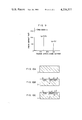
- numerals 1, 2 and 3 denote an anode electrode, a cathode electrode and a gate electrode, respectively, while numeral 4 denotes a cathode region, 5 denotes a gate region, 6 denotes an anode region, and 7 denotes a semiconductor substrate.
- a positive voltage is applied to the anode with a negative voltage applied to the cathode electrode
- the thyristor takes a blocking or non-conducting state so far as the gate electrode is closed.
- a voltage v a which increases as a function of time (i.e. a voltage having a positive value of dv a /dt) is applied to the anode electrode 1
- a displacement current is produced and flows from the anode electrode 1 to the cathode electrode 2.
- This displacement current will then act as a gate trigger current to drive undesirably the thyristor into the conducting state.
- Such phenomenon provides a serious problem particularly in applications in which the thyristor is employed in a circuit subjected to various noises and/or operated at a high switching frequency, involving a degraded reliability of the thyristor and imposing restriction to a desired high speed operation.
- An object of the invention is therefore to provide a semiconductor switching device of a novel structure which evades the drawbacks of the hitherto known switching elements and is highly capable of withstanding dv/dt-effect and can be inplemented with a high integration density.
- a semiconductor switching device which includes a semiconductor substrate of a first conductivity type having an anode region of a second conductivity type opposite to the first conductivity type formed in the semiconductor substrate adjacent to a major surface, a gate region formed adjacent to the major surface with a distance from the anode region and having a channel region of a predetermined width and depth and a cathode region formed in the gate region adjacent to the major surface so as to be directly contacted to the semiconductor substrate through the channel region, wherein a current path leading from the anode region to the cathode region through the substrate is interrupted by a depletion layer produced within the substrate in the vicinity of the channel region upon application of a reverse bias voltage between the gate and the cathode electrode. In the absence of the reverse bias voltage, the anode region, the semiconductor substrate, the gate and the cathode region cooperate to function as a thyristor.
- FIG. 1 is a schematic sectional view showing a structure of a conventional semiconductor switching device.
- FIG. 2 is a schematic sectional view of a semiconductor switching device according to an embodiment of the invention.
- FIGS. 3A and 4A are top plan views showing electrode array patterns for the semiconductor switching device shown in FIG. 2.
- FIG. 3B is a sectional view taken along the line IIIB-IIIB' in FIG. 3A.
- FIG. 4B is a sectional view taken along the line IVB-IVB' in FIG. 4A.
- FIG. 3C is a sectional view taken along the line IIIC-IIIC' in FIG. 3A.
- FIG. 4C is a sectional view taken along the line IVC-IVC' in FIG. 4A.
- FIG. 5A is a top plan view of a semiconductor switching device according to another embodiment to the present invention.
- FIGS. 5B and 5C are sectional views taken along lines VB-VB' and VC-V' in FIG. 5A, respectively.
- FIG. 6A in a top plan view of a semiconductor switching device according to further embodiment according to the present invention.
- FIGS. 6B and 6C are sectional views taken along lines VIB-VIB' and VIC-VIC' in FIG. 6A, respectively.
- FIGS. 7 to 8 show yet further embodiments of the present invention.
- FIG. 9 graphically illustrates operation characteristics of the semiconductor switching device according to the present invention.
- FIGS. 10A to 10C illustrate manufacturing steps for fabricating the semiconductor switching device shown in FIG. 2.
- FIG. 2 shows schematically a sectional structure of a semiconductor switching device according to an embodiment of the invention.
- the same reference numerals are applied to like parts as in FIG. 1.
- an anode region 6 of p + -conductivity type and a cathode region 4 of n + -type conductivity are provided at a same major surface of a semiconductor substrate of n-conductivity type.
- a gate region 5 of p + -conductivity type is so provided as to be partially exposed around the cathode region 4 at the major surface and forms a groove or channel region 9 of n-conductivity type immediately below the n + -cathode region 4.
- the n + -cathode region 4 is directly connected to the n-substrate 7 through the n-channel region 9.
- the anode region, the cathode region, the gate region and the channel region are each formed in a strip-like configuration.
- a plurality of the switching devices of this structure may be provided in a single semiconductor wafer, each being formed in an island or well isolated from the others by a pn-junction layer or alternatively by an insulating or dielectric layer and interconnected in desired manner.
- Arrays of electrodes for the anode region, the cathode region and the gate region may practically be implemented in simplified patterns shown in FIGS.
- FIGS. 3A, 3B and 3C and FIGS. 4A, 4B and 4C the same reference numerals are applied to the like parts as in FIG. 2.
- reference numeral 10 denotes a film of SiO 2 which does not appear in FIGS. 3A and 4A.
- the n-channel region 9 is shown as lying within the boundary of the cathode region 4 in FIGS. 3A and 3C, it should be understood that the n-channel region may extend longitudinally beyond the cathode region 9 into the substrate region as shown in FIGS. 4A and 4C.
- the channel region 9 should preferably be positioned in a longitudinal alignment with and immediately below a middle portion of the cathode region 4 as seen from FIGS. 3A, 3C and 4A, 4C in order to assure a symmetrical current extraction and prevent non-uniformity in a current density when the switching device is turned off.
- the width d 1 of the channel 9 is so selected as to be narrower than the widths d 2 , d 3 of the lower surface of the cathode region 4 opposed to the major surface at both longitudinal sides of the channel region 9 as measured from the respective longitudinal edges of the channel region 9 in the width direction thereof. This arrangement is particularly important for enhancing the action and effect envisaged by the invention, as will be made more apparent as description proceeds.
- FIGS. 5A, 5B, 5C shows another embodiment of a semiconductor switching device of this invention in which a plurality of channels (for example, 4 channels as seen from the figure) are provided.
- a gate region 5 is integrally formed to surround a plurality of strip-like cathode regions 4 spaced apart from each other and arranged in parallel.
- the plurality of channel regions 9 are provided beneath the respective cathode regions.
- An anode electrode 1, a comb-like cathode electrode 2, and a comb-like gate electrode 3 are kept in ohmic contact with the anode region 6, the cathode regions 4 and the gate region 5.
- the comb-like cathode electrode 2 and the comb-like gate electrode 3 are arranged in interdigitated form.
- the divergent arrangement of the gate electrode in such interdigitated form provides a small voltage drop in the gate region 5, which makes easy a gate turn-off action.
- a plurality of anode regions may be arranged. Namely, as shown in a phantom line in FIG. 5A another anode region 6' may be added, which advantageously expands a current path and decreases a forward voltage drop.
- FIGS. 6A, 6B, 6C show further embodiment of a semiconductor switching device of this invention which is a modification of FIGS. 5A, 5B, 5C and in which a high impurity region 12 of n + conductivity type is provided to be adjacent to the anode region 6 at at least one portion thereof in an area in the main surface opposite to the gate region 5, and the anode electrode 1 is kept in ohmic contact to both the anode region 6 and the high impurity region 12.
- FIGS. 6A, 6B, 6C the same reference numerals are applied to like parts as in FIGS. 5A, 5B, 5C. This structure provides the following effects.
- the high impurity region 12 stops a depletion layer which may extend from the gate region 5, which enhances the breakdown voltage of the device.
- the charges stored in the base region (the substrate 7) at the time of turn-off of the device are derived through the high impurity region 12 to the anode electrode 1 and annihilated there, which provides a short turn off time. It is of course that the above arrangement of the high impurity region 12 and the anode electrode 6 are also applied to the embodiments of FIGS. 3A, 3B, 3C and 4A, 4B, 4C.
- the gate electrode 3 is connected to a negative pole of a power supply source of voltage V g with the cathode electrode 2 connected to a positive pole of the power supply source so that a junction J3 is biased reversely or backwardly when a switch S is closed. Under this condition, there will be produced a depletion layer 11 as indicated by a dashed line.
- the spatial extension of the depletion layer 11 is in general restricted in the regions other than the n-channel region 9, which can be explained by the fact that the impurity concentrations of the p + -gate region 5 and the n + -cathode region 4 are selected relatively higher than that of the n-channel region 9 which is equal to the impurity concentration of the n-semiconductor substrate 7.
- the width d 1 and depth l of the n-channel region 9 as well as the voltage V g of the power supply source are selected at appropriate values, the n-channel region 9 can be perfectly pinched off by the depletion layer 11.
- the depletion layer 11 extending into the n-channel region 9 will then disappear, resulting in the current being allowed to flow from the anode electrode 1 to the cathode electrode 2 through the n-channel region 9 upon application of a positive voltage onto the anode electrode 1 relative to the cathode electrode 2.
- the n-channel region 9 will then function as a diode, while the other portions cooperates with one another to function as a thyristor, whereby current flows into all the region of the n + -cathode region 4.
- Such thyristor operation will result in an increased conducting area of the device and significantly reduce the turn-on voltage to a great advantage.
- FIG. 9 graphically illustrates characteristics of the switching device according to an embodiment of the invention in which the dimensions d 1 and l described hereinbefore have been selected equal to 3 ⁇ m and 5 ⁇ m, respectively.
- the potential barrier produced in the n-channel region 9 is cleared by the electric field of the depletion layer 11 extending from the junction J2 around the p + -gate region 5 toward the p + -anode region 6, thereby to eventually allow the current to start flowing.
- the anode voltage which can be blocked by increasing the gate voltage will increase in a manner illustrated in FIG. 9.
- there is an upper limit imposed on the forward blocking voltage since the voltage applied across the gate-cathode path is subjected to a limit.
- the pintch-off voltage can be correspondingly decreased, which means that a high anode voltage can be blocked with the aid of a relatively low gate voltage.
- the gate voltage can be made lower, as the depth l of the n-channel region 9 is selected greater.
- optimum values for the width and the depth of the n-channel 9 are selected in consideration of the reproducibility of the fabricating process as well as the thickness of the p + -gate region 5 of the thyristor switch.
- a characteristic feature of the switching device according to the invention can be seen in a composite structure including a lateral thyristor and a field controlled switching device, which is very advantageous in that a high dv/dt-capability can be attained and that integrated structure can be easily realized.
- the invention teaches the structure which can eliminate the need for provision of such n-type layer to assure more effective thyristor operation and allow a larger current to be processed. Further, according to the teaching of the invention, the n-channel width can be made narrower, while the area of the cathode region can be made larger than the exposed area of the gate region. Consequently, a large current can be turned on and off with a relatively low gate voltage and a relatively small area of the gate region at a relatively high integration density of the integrated structure.
- difficulty may be encountered in attaining an impurity concentration of an epitaxially grown layer equal to or lower than that of the substrate.
- an epitaxially grown layer having an impurity concentration of 1 ⁇ 10 13 cm -3 is to be formed in a semiconductor substrate having an impurity concentration of 1 ⁇ 10 15 cm -3
- Such high resistivity layer allows therein an abnormal instrusion of the depletion layer extending between the anode region and the gate region, involving the problem of punch-through and reducing a breakdown voltage.
- the inversion layer provides an obstacle in forming the channel in a satisfactory or normal manner and at the same time gives rise to a short-circuited state between the anode electrode and the gate electrode. Even if the fatal characteristic abnormalities due to the auto-doping could be prevented from ocurring. Stacking faults and misfit dislocations will often take place at the interface between the substrate and the epitaxially grown layer, involving possibly degradation in the breakdown voltage and increase in the leak current.
- the lateral type semiconductor switching device can be fabricated simply by a selective diffusion technique through treatments such as diffusion, evaporating electrode deposition and so forth advantageously for easy integration. Additionally, no dv/dt compensating circuit is required, a correspondingly increased integration density can be attained.
- an n-semiconductor substrate 7 (FIG. 10A) is prepared which has preferably impurity concentration of 5 ⁇ 10 14 atoms/cm 3 and thickness not smaller than 50 ⁇ m. Then the p + -anode region 6 and the p + -gate region 5 are formed through selective diffusion of p + -type impurity such as boron, for example, from one major surface simultaneously with the formation of the n-channel region 9 (FIG. 10B).
- the anode region 6 may be of a p + -type diffused layer of 150 ⁇ m in width, 300 ⁇ m in length and 15 ⁇ m in depth or thickness.
- the p + -gate region 5 may be of a p + -diffused layer of 150 ⁇ m wide, 300 ⁇ m thick.
- the impurity concentration in the regions adjacent to the major surface is selected on the order of 5 ⁇ 10 13 atoms/cm 3 so that switching operation can be effected at the pnpn-junctions obtained when the n + -cathode region 4 has been formed through diffusion.
- the processes described so far may be accomplished by placing a boronnitride wafer and a silicon wafer in a quartz tube and holding at a temperature of about 950° C. for about 30 minutes in the atmosphere of an inert gas and subsequently heating the silicon wafer at about 1200° C. for about four hours in an oxidiging atmosphere.
- the p + -anode region 6 and the p + -gate region 5 are formed in the major surface in opposition to each other with a distance of about 100 ⁇ m therebetween.
- the n-channel region 9 formed in the p + -gate region 5 should preferably have a width of 3 ⁇ m and length of 260 ⁇ m.
- the n + -cathode region 4 is formed through selective diffusion of an n + -impurity such as phosphorus, for example.
- an n + -impurity such as phosphorus
- the surface dimension is selected to be of 80 ⁇ m ⁇ 280 ⁇ m with a thickness of 10 ⁇ m
- the n + -cathode region 4 is implemented in a structure surrounded by the p + -gate region 5 except for the portion corresponding to the n-channel region 9 (FIG. 10C).
- vapor of POCl 3 may be introduced onto the silicon substrated in a heated state. For example, by such thermal treatment at 950° C.
- the phosphorus diffused layer can be formed which has a high impurity concentration in the cathode region adajent to the major surface.
- the semiconductor substrate thus obtained is subjected to a thermal treatment at 1200° C. for 60 minutes in an oxidizing atmosphere thereby to form ultimately the n + -cathode region 4 of 10 ⁇ m in depth having the surface impurity concentration of 2 ⁇ 10 20 atoms/cm 3 .
- the electrodes 1, 2 and 3 are contacted to the p + -anode region 6, the n + -cathode region 4 and the p + -gate region 5, respectively, to accomplish the switching device of the structure according to the invention as shown in FIG. 2.
- the metallic electrodes may be formed of aluminium films of 2 ⁇ m thick through evaporation, for example.
- the width of the anode electrode 1 and the cathode electrode 2 should preferably on the order of 60 ⁇ m, while the gate electrode 3 should preferably be formed of an aluminium film having width of + ⁇ m in the case of the illustrated embodiment.
- a thyristor unit of p + np + n + -structure and a diode unit of p + nn + -structure have been implemented in parallel to each other in the current path extending from the anode region 6 to the cathode region 4.
- FIG. 9 graphically shows the typical characteristics of a switching device actually fabricated according to the manufacturing process described above.
- the invention has now proposed a novel semiconductor switching device in which the thyristor and the diode are caused to operate in parallel to each other in the conducting state, while non-conducting or blocking state is brought about by pinch off of the channel region under the electric field control to interrupt the current flow.
- description will be made on advantageous feature of the switching device according to the invention by comparing with conventional switching devices in order to have a better understanding of the invention.
- comparison will be made with a conventional semiconductor switch which incorporates a transistor as a switching device. The switching transistor is turned on upon application of a base current and turned off when the base current becomes zero. Accordingly, a current supply circuit is inevitably required in order to maintain the transistor switch in the conducting state.
- the transition from the non-conducting state to the conducting state or vice versa can be effected merely by applying or removing the gate voltage without requiring any appreciable driving power.
- a current will flow in the gate circuit even in the switching device according to the invention when the switching operation is made to go from the conducting to the non-conducting state.
- the duration of such current flow is extremely short and involves no appreciable power consumption.
- the switching device according to the invention exhibits a very high ratio of the power required for the control to the power to be controlled, which is a very advantageous and desirable characteristic for a switching device.
- the switching device according to the invention exhibits a high withstanding capability against a surge current and an excellent reliability as the switching device without sufferring from the secondary break-down phenomenon.
- the advantages of the switching device according to the invention over the conventional thyristor structure such as shown in FIG. 1 will be obvious from the description made hereinbefore.
- the main current path is constituted only by the channel as a result of which a narrow width of the channel region will often give rise to an increaed turn-on voltage.
- the channel region has been realized in a plurality of separate sub-channels, which however means that precise and elaborate treatments are required for the fabrication of the field controlled thyristor in a much complicated process.
- the main current flows through the thyristor structure with the p + nn + -type diode structure being subjected to only a small fraction of the main current for turning on the thyristor.
- the cathode region can be implemented in a relatively large dimension by virtue of such structure in which the cathode region is commonly shared by the thyristor and the diode, as shown in FIG. 8.
- the manufacturing process can be much simplified. In reality, a locally fine diffusion mask pattern is required only when the channel region is formed. The other fabricating steps can be carried out in the substantially same way as the conventional thyristors.
- the thyristor portion should preferably have a larger area than that of the diode portion formed by the channel region at least below the lower surface of the cathode region opposite to the major surface to flow the main current through the thyristor portion in order to make the various advantages described above to be available at maximum.
- n-channel regions 9 may be provided in order to evade current concentration upon turn-on operation of the switching device.
Landscapes
- Engineering & Computer Science (AREA)
- Microelectronics & Electronic Packaging (AREA)
- Power Engineering (AREA)
- Physics & Mathematics (AREA)
- Ceramic Engineering (AREA)
- Condensed Matter Physics & Semiconductors (AREA)
- General Physics & Mathematics (AREA)
- Computer Hardware Design (AREA)
- Thyristors (AREA)
Applications Claiming Priority (2)
| Application Number | Priority Date | Filing Date | Title |
|---|---|---|---|
| JP53028252A JPS5936832B2 (ja) | 1978-03-14 | 1978-03-14 | 半導体スイッチング素子 |
| JP53/28252 | 1978-03-14 |
Publications (1)
| Publication Number | Publication Date |
|---|---|
| US4258377A true US4258377A (en) | 1981-03-24 |
Family
ID=12243373
Family Applications (1)
| Application Number | Title | Priority Date | Filing Date |
|---|---|---|---|
| US06/019,567 Expired - Lifetime US4258377A (en) | 1978-03-14 | 1979-03-12 | Lateral field controlled thyristor |
Country Status (3)
| Country | Link |
|---|---|
| US (1) | US4258377A (de) |
| JP (1) | JPS5936832B2 (de) |
| DE (1) | DE2909795C2 (de) |
Cited By (4)
| Publication number | Priority date | Publication date | Assignee | Title |
|---|---|---|---|---|
| US4567500A (en) * | 1981-12-01 | 1986-01-28 | Rca Corporation | Semiconductor structure for protecting integrated circuit devices |
| US4831423A (en) * | 1985-03-29 | 1989-05-16 | U.S. Philips Corporation | Semiconductor devices employing conductivity modulation |
| US5581096A (en) * | 1993-12-10 | 1996-12-03 | Robert Bosch Gmbh | Integrated semiconductor device having a thyristor |
| US5793066A (en) * | 1995-09-26 | 1998-08-11 | International Rectifier Corporation | Base resistance controlled thyristor structure with high-density layout for increased current capacity |
Families Citing this family (1)
| Publication number | Priority date | Publication date | Assignee | Title |
|---|---|---|---|---|
| US4779126A (en) * | 1983-11-25 | 1988-10-18 | International Rectifier Corporation | Optically triggered lateral thyristor with auxiliary region |
Citations (9)
| Publication number | Priority date | Publication date | Assignee | Title |
|---|---|---|---|---|
| US3475666A (en) * | 1966-08-15 | 1969-10-28 | Jearld L Hutson | Integrated semiconductor switch system |
| US3617828A (en) * | 1969-09-24 | 1971-11-02 | Gen Electric | Semiconductor unijunction transistor device having a controlled cross-sectional area base contact region |
| US3911463A (en) * | 1974-01-07 | 1975-10-07 | Gen Electric | Planar unijunction transistor |
| US3958268A (en) * | 1973-05-08 | 1976-05-18 | Hitachi, Ltd. | Thyristor highly proof against time rate of change of voltage |
| US3972061A (en) * | 1974-10-02 | 1976-07-27 | National Semiconductor Corporation | Monolithic lateral S.C.R. having reduced "on" resistance |
| US3986904A (en) * | 1972-07-21 | 1976-10-19 | Harris Corporation | Process for fabricating planar scr structure |
| US4060821A (en) * | 1976-06-21 | 1977-11-29 | General Electric Co. | Field controlled thyristor with buried grid |
| DE2734997A1 (de) * | 1976-08-03 | 1978-02-16 | Zaidan Hojin Handotai Kenkyu | Integrierte halbleiterschaltung |
| US4150391A (en) * | 1976-09-03 | 1979-04-17 | Bbc Brown, Boveri & Company, Limited | Gate-controlled reverse conducting thyristor |
Family Cites Families (1)
| Publication number | Priority date | Publication date | Assignee | Title |
|---|---|---|---|---|
| US3742318A (en) * | 1970-11-26 | 1973-06-26 | Matsushita Electric Ind Co Ltd | Field effect semiconductor device |
-
1978
- 1978-03-14 JP JP53028252A patent/JPS5936832B2/ja not_active Expired
-
1979
- 1979-03-12 US US06/019,567 patent/US4258377A/en not_active Expired - Lifetime
- 1979-03-13 DE DE2909795A patent/DE2909795C2/de not_active Expired
Patent Citations (9)
| Publication number | Priority date | Publication date | Assignee | Title |
|---|---|---|---|---|
| US3475666A (en) * | 1966-08-15 | 1969-10-28 | Jearld L Hutson | Integrated semiconductor switch system |
| US3617828A (en) * | 1969-09-24 | 1971-11-02 | Gen Electric | Semiconductor unijunction transistor device having a controlled cross-sectional area base contact region |
| US3986904A (en) * | 1972-07-21 | 1976-10-19 | Harris Corporation | Process for fabricating planar scr structure |
| US3958268A (en) * | 1973-05-08 | 1976-05-18 | Hitachi, Ltd. | Thyristor highly proof against time rate of change of voltage |
| US3911463A (en) * | 1974-01-07 | 1975-10-07 | Gen Electric | Planar unijunction transistor |
| US3972061A (en) * | 1974-10-02 | 1976-07-27 | National Semiconductor Corporation | Monolithic lateral S.C.R. having reduced "on" resistance |
| US4060821A (en) * | 1976-06-21 | 1977-11-29 | General Electric Co. | Field controlled thyristor with buried grid |
| DE2734997A1 (de) * | 1976-08-03 | 1978-02-16 | Zaidan Hojin Handotai Kenkyu | Integrierte halbleiterschaltung |
| US4150391A (en) * | 1976-09-03 | 1979-04-17 | Bbc Brown, Boveri & Company, Limited | Gate-controlled reverse conducting thyristor |
Non-Patent Citations (2)
| Title |
|---|
| H. Berger et al., "Base Ring Transistor and Method of Production" IBM Tech. Discl. Bull., vol. 14, #1, Jun. 1971, p. 302. * |
| J. Nishizawa et al., "Static Induction . . . Density," Jap. J. of Appl. Phys., vol. 16 (1977) Supplement 16-1, pp. 151-154. * |
Cited By (4)
| Publication number | Priority date | Publication date | Assignee | Title |
|---|---|---|---|---|
| US4567500A (en) * | 1981-12-01 | 1986-01-28 | Rca Corporation | Semiconductor structure for protecting integrated circuit devices |
| US4831423A (en) * | 1985-03-29 | 1989-05-16 | U.S. Philips Corporation | Semiconductor devices employing conductivity modulation |
| US5581096A (en) * | 1993-12-10 | 1996-12-03 | Robert Bosch Gmbh | Integrated semiconductor device having a thyristor |
| US5793066A (en) * | 1995-09-26 | 1998-08-11 | International Rectifier Corporation | Base resistance controlled thyristor structure with high-density layout for increased current capacity |
Also Published As
| Publication number | Publication date |
|---|---|
| JPS5936832B2 (ja) | 1984-09-06 |
| JPS54121074A (en) | 1979-09-19 |
| DE2909795C2 (de) | 1986-07-31 |
| DE2909795A1 (de) | 1979-09-20 |
Similar Documents
| Publication | Publication Date | Title |
|---|---|---|
| US4145703A (en) | High power MOS device and fabrication method therefor | |
| US4450467A (en) | Gate turn-off thyristor with selective anode penetrating shorts | |
| US4223328A (en) | Field controlled thyristor with dual resistivity field layer | |
| US4060821A (en) | Field controlled thyristor with buried grid | |
| JPH037149B2 (de) | ||
| KR100661691B1 (ko) | 접합형 전계 효과 트랜지스터 및 그 제조 방법 | |
| JPH0690009A (ja) | 半導体装置 | |
| US4398339A (en) | Fabrication method for high power MOS device | |
| US4086611A (en) | Static induction type thyristor | |
| US5291040A (en) | Deactivatable thyristor with turn-off current path | |
| US4171995A (en) | Epitaxial deposition process for producing an electrostatic induction type thyristor | |
| EP0014080B1 (de) | Halbleiterschaltungs-Vorrichtung mit drei Klemmen | |
| US4258377A (en) | Lateral field controlled thyristor | |
| US3312880A (en) | Four-layer semiconductor switching device having turn-on and turn-off gain | |
| EP0872894A2 (de) | Statischer Induktionstransistor und Ansteuerungsverfahren und Ansteuerungsschaltung davon | |
| EP0064614A2 (de) | Emitterstruktur für Halbleiteranordnungen | |
| JPS6124832B2 (de) | ||
| US4651188A (en) | Semiconductor device with specifically oriented control layer | |
| JPS6153877B2 (de) | ||
| US3697830A (en) | Semiconductor switching device | |
| US20070114565A1 (en) | Integrated field-effect transistor-thyristor device | |
| US5420046A (en) | Method for manufacturing optically triggered lateral thyristor | |
| JPS639386B2 (de) | ||
| US4667215A (en) | Semiconductor device | |
| JP2630088B2 (ja) | ゲートターンオフサイリスタ |