US4166258A - Thin-film integrated circuit with tank circuit characteristics and applications to thin-film filters and oscillators - Google Patents
Thin-film integrated circuit with tank circuit characteristics and applications to thin-film filters and oscillators Download PDFInfo
- Publication number
- US4166258A US4166258A US05/501,552 US50155274A US4166258A US 4166258 A US4166258 A US 4166258A US 50155274 A US50155274 A US 50155274A US 4166258 A US4166258 A US 4166258A
- Authority
- US
- United States
- Prior art keywords
- surface acoustic
- conductors
- acoustic wave
- pair
- substrate
- Prior art date
- Legal status (The legal status is an assumption and is not a legal conclusion. Google has not performed a legal analysis and makes no representation as to the accuracy of the status listed.)
- Expired - Lifetime
Links
- 239000010409 thin film Substances 0.000 title claims abstract description 21
- 238000010897 surface acoustic wave method Methods 0.000 claims abstract description 49
- 239000004020 conductor Substances 0.000 claims description 110
- 239000000758 substrate Substances 0.000 claims description 35
- 230000002463 transducing effect Effects 0.000 claims description 11
- 230000001747 exhibiting effect Effects 0.000 claims description 8
- 239000003989 dielectric material Substances 0.000 claims 1
- 239000003990 capacitor Substances 0.000 description 13
- 230000001965 increasing effect Effects 0.000 description 12
- 239000000463 material Substances 0.000 description 12
- 230000001939 inductive effect Effects 0.000 description 11
- 230000003068 static effect Effects 0.000 description 11
- 229920002120 photoresistant polymer Polymers 0.000 description 7
- 230000004044 response Effects 0.000 description 7
- 238000000034 method Methods 0.000 description 6
- 230000005684 electric field Effects 0.000 description 4
- 238000010894 electron beam technology Methods 0.000 description 4
- 238000004519 manufacturing process Methods 0.000 description 4
- 230000010355 oscillation Effects 0.000 description 4
- 238000010586 diagram Methods 0.000 description 3
- 239000010408 film Substances 0.000 description 3
- XAGFODPZIPBFFR-UHFFFAOYSA-N aluminium Chemical compound [Al] XAGFODPZIPBFFR-UHFFFAOYSA-N 0.000 description 2
- 229910052782 aluminium Inorganic materials 0.000 description 2
- 230000008901 benefit Effects 0.000 description 2
- 230000003247 decreasing effect Effects 0.000 description 2
- 230000001419 dependent effect Effects 0.000 description 2
- PCHJSUWPFVWCPO-UHFFFAOYSA-N gold Chemical compound [Au] PCHJSUWPFVWCPO-UHFFFAOYSA-N 0.000 description 2
- 229910052737 gold Inorganic materials 0.000 description 2
- 239000010931 gold Substances 0.000 description 2
- 230000007246 mechanism Effects 0.000 description 2
- 230000001902 propagating effect Effects 0.000 description 2
- WHXSMMKQMYFTQS-UHFFFAOYSA-N Lithium Chemical compound [Li] WHXSMMKQMYFTQS-UHFFFAOYSA-N 0.000 description 1
- 230000009471 action Effects 0.000 description 1
- 238000013459 approach Methods 0.000 description 1
- 230000008859 change Effects 0.000 description 1
- 230000001427 coherent effect Effects 0.000 description 1
- 238000007796 conventional method Methods 0.000 description 1
- 238000005516 engineering process Methods 0.000 description 1
- 238000001704 evaporation Methods 0.000 description 1
- 238000002474 experimental method Methods 0.000 description 1
- 238000001914 filtration Methods 0.000 description 1
- 230000006872 improvement Effects 0.000 description 1
- 229910052744 lithium Inorganic materials 0.000 description 1
- 230000004048 modification Effects 0.000 description 1
- 238000012986 modification Methods 0.000 description 1
- 230000009467 reduction Effects 0.000 description 1
Images


Classifications
-
- H—ELECTRICITY
- H03—ELECTRONIC CIRCUITRY
- H03H—IMPEDANCE NETWORKS, e.g. RESONANT CIRCUITS; RESONATORS
- H03H9/00—Networks comprising electromechanical or electro-acoustic elements; Electromechanical resonators
- H03H9/02—Details
- H03H9/02535—Details of surface acoustic wave devices
- H03H9/02637—Details concerning reflective or coupling arrays
- H03H9/02685—Grating lines having particular arrangements
- H03H9/02692—Arched grating lines
- H03H9/027—U-shaped grating lines
-
- H—ELECTRICITY
- H03—ELECTRONIC CIRCUITRY
- H03H—IMPEDANCE NETWORKS, e.g. RESONANT CIRCUITS; RESONATORS
- H03H9/00—Networks comprising electromechanical or electro-acoustic elements; Electromechanical resonators
- H03H9/46—Filters
- H03H9/64—Filters using surface acoustic waves
- H03H9/6423—Means for obtaining a particular transfer characteristic
- H03H9/6433—Coupled resonator filters
- H03H9/6483—Ladder SAW filters
-
- H—ELECTRICITY
- H03—ELECTRONIC CIRCUITRY
- H03H—IMPEDANCE NETWORKS, e.g. RESONANT CIRCUITS; RESONATORS
- H03H9/00—Networks comprising electromechanical or electro-acoustic elements; Electromechanical resonators
- H03H9/02—Details
- H03H9/125—Driving means, e.g. electrodes, coils
- H03H9/145—Driving means, e.g. electrodes, coils for networks using surface acoustic waves
- H03H9/14517—Means for weighting
- H03H9/1452—Means for weighting by finger overlap length, apodisation
Definitions
- These devices comprise a pattern of conductors on a piezoelectric substrate.
- the pattern of conductors comprises a pair of parallel opposed, spaced conductors each of which has a number of so-called interdigital electrodes orthogonal to and connected to the conductor.
- the interdigital electrodes have a length which is less than the spacing between the conductors and are all parallel to one another. Adjacent ones of the interdigital electrodes are connected to alternate ones of the conductors.
- each requires a pair of surface acoustic wave transducing means to be deposited on the substrate. Furthermore, they require a certain amount of piezoelectric material to couple the surface acoustic waves generated by one transducer to the other transducer. Furthermore, there is a desire to sharpen the impedance characteristics of the device so that it could be used, for instance, as a tank circuit to form a basic building block for filter and oscillator applications.
- Another frequency selective device which employs acoustic waves is the bulk-wave transducer.
- an electric field generated between two spaced electrodes is coupled through a piezoelectric material.
- the frequency response of the device is very sharp.
- the electric field is applied across the piezoelectric material the frequency response is directly dependent upon the thickness of the material between the electrodes.
- accurate dimensions for the piezoelectric material are essential.
- the thickness of the device must decrease. With present day technology the frequency range for bulk-wave piezoelectric devices is about 20 megahertz with an upper limit of 100 megahertz.
- the present invention provides a two terminal thin-film integrated circuit exhibiting tank circuit characteristics. It includes a single surface acoustic wave transducing means which may have characteristics similar to those exhibited by the prior art.
- the transducer will have a pair of parallel conductors deposited on a piezoelectric substrate. Each of the conductors has connected thereto a plurality of orthogonal interdigital electrodes also deposited on the substrate. Adjacent ones of the interdigital electrodes are connected to different ones of the conductors. By increasing the number of interdigital electrodes the device will exhibit inductive reactance in a frequency range between a resonant and anti-resonant frequency.
- surface acoustic wave reflecting means are also provided on the substrate adjacent the surface acoustic wave (hereinafter SAW) transducer.
- the reflecting means enhance the inductive reactance of the device.
- the SAW reflecting means preferably includes a pair of SAW reflectors, each of which is located on opposite sides of the transducer.
- the reflectors may comprise a series of conductors, parallel to the interdigital electrodes.
- the reflectors may comprise a series of grooves, parallel to the interdigital electrodes.
- the reflectors may be provided by a series of parallel weighty dielectric bars placed atop the substrate. Regardless of the particular configuration of the reflectors the spacing between each of the different reflector elements would be equal.
- spacing of the reflector elements is made a quarter wavelength of the resonant frequency.
- frequency response becomes wide band and the entire device exhibits the characteristics of a multiple tank circuit, i.e., one with multiple resonant-anti-resonant frequency pairs.
- reflectors are preferable for they increase the inductive reactance of the device without increasing the capacitive reactance.
- Another novel SAW transducer which exhibits a lower equivalent capacitance is also useful in devices exhibiting tank circuit characteristics.
- the novel SAW transducer may be used with or without the reflecting means referred to above, although preferably the reflecting means are used.
- the novel SAW transducer has at least three parallel conductors, two of which are co-linear. Each of these conductors has connected thereto a number of interdigital electrodes orthogonal to the conductors.
- the co-linear conductors are spaced so as not to be electrically conductive. Adjacent ones of the interdigital electrodes are connected alternately to spaced conductors except in the region where a gap exists between two co-linear conductors. In this region, two adjacent interdigital electrodes are connected to the same conductor opposite the gap between the two co-linear conductors.
- a plurality of SAW devices each of which exhibits tank circuit characteristics can be deposited on a single piezoelectric substrate and electrically interconnected by deposited conductors to exhibit filter characteristics. Also, the device can be connected as a feedback element between input and output terminals of an amplifier to thereby comprise an oscillator. The frequency or frequencies of oscillation of the oscillator are then determined by the frequency response characteristics of the device.
- FIG. 1 is a plan view of a prior art surface acoustic wave device
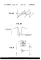
- FIG. 2A is a plan view of a surface acoustic wave device in accordance with the principles of this invention which exhibits tank circuit characteristics;
- FIG. 2B is an equivalent circuit diagram of the electrical characteristics of the device shown in FIG. 2A;
- FIG. 2C is a graphical illustration of the impedance versus frequency characteristics of the device illustrated in FIG. 2A;
- FIG. 3A is a plan view of a preferred embodiment of the present invention.
- FIGS. 3B and 3C are cross sections of two respective embodiments for the plan view illustrated in FIG. 3A;
- FIG. 3D is a plan view of still another preferred embodiment of our invention.
- FIG. 4A is a plan view of a novel SAW transducer of my invention.
- FIGS. 4B and 4C are equivalent circuit diagrams useful in explaining the advantage of the novel SAW transducer
- FIG. 5A is a plan view of a surface acoustic wave filter which has the characteristics of a T circuit
- FIG. 5B is an equivalent electrical circuit diagram of the device shown in FIG. 5A;
- FIG. 5C is a plot of impedance versus frequency for the components of the equivalent circuit shown in FIG. 5B;
- FIG. 5D is a plot of attenuation versus frequency for the device illustrated in FIG. 5A.
- FIG. 6 is a schematic representation of an oscillator using the surface acoustic wave device of my invention.
- FIG. 1 illustrates a prior art two port, four terminal SAW device.
- This device 10 has input terminals 1-1' and output terminals 2-2'.
- a pair of parallel conductors 5 and 6 comprising a first SAW transducer are connected, respectively, to input terminals 1 and 1'.
- a plurality of interdigital electrodes 3 Connected to each of the conductors 5 and 6 are a plurality of interdigital electrodes 3 which may have been deposited on the substrate. As is illustrated in FIG. 1, adjacent ones of the interdigital electrodes 3 are connected to different conductors.
- an electrical voltage is applied between terminals 1 and 1' an electric field is generated by the voltage and generates a surface acoustic wave by reason of the piezoelectric quality of the material 4. This surface acoustic wave is diagrammatically shown by the arrows 9.
- a second SAW transducer is included in the device 10.
- This second transducer includes a second pair of parallel conductors 7 and 8 which are respectively connected to the output terminals 2 and 2'.
- a plurality of interdigital electrodes 11 are connected to the parallel conductors 7 and 8 with the interdigital electrodes 11 perpendicular to the conductors 7 and 8.
- Adjacent interdigital electrodes 11 are connected to different ones of the conductors 7 and 8.
- the surface acoustic wave generated by the first transducer is converted into an electrical potential by the piezoelectric material 4 which is coupled to interdigital electrodes 11. This potential is available at terminals 2 and 2'.
- FIG. 2A is a schematic illustration of a surface acoustic wave device in accordance with the principles of my invention.
- a substrate 4 of piezoelectric material such as lithium niobrate
- interdigital electrodes 18 are also connected to conductors 16 and 17. As is illustrated in FIG. 2A adjacent interdigital electrodes 18 are connected to different ones of the conductors 16 and 17.
- the SAW device of my invention In order for the SAW device of my invention to exhibit the electrical characteristics of a tank circuit its electrical impedance must change from a capacitive reactance to an inductive reactance at certain frequencies.
- My experiments have shown that the number of interdigital electrodes, and therefore the length of the conductors that they are connected to, must be increased over the number employed in the prior art SAW transducer for the device to exhibit sufficient inductive reactance.
- the device When constructed in accordance with the principles of my invention the device will have electrical characteristics which can be described by using the equivalent circuit of FIG. 2B. In particular, the device will act as the parallel combination of a capacitance C O connected across a serial combination of an inductance L and capacitance C r .
- the impedance variation, with frequency, of this equivalent circuit is illustrated in FIG. 2C.
- the impedance of the equivalent circuit of FIG. 2B is capacitive in a range of frequencies from O to F r .
- F r is known as the resonant frequency of the equivalent circuit for it is at this frequency that the circuit exhibits minimal impedance.
- the equivalent impedance of the device of FIG. 2A is inductive in a range of frequencies from F r to F a .
- F a is known as the anti-resonant frequency of the circuit, i.e., the frequency at which the circuit exhibits infinite, i.e., large, impedance. Above the anti-resonant frequency the device again exhibits capacitive reactance.
- the resonant frequency F r is determined by the periodicity of the interdigital electrodes, the interdigital electrode width and the spacing between the interdigital electrodes.
- the anti-resonant frequency is determined by the foregoing parameters and the electromechanical properties of the material used for the substrate.
- the wavelength for any particular frequency depends upon the piezoelectric material.
- the conductors 16 and 17 and the interdigital electrodes 18 can comprise a metallic film such as gold or aluminum.
- the device of FIG. 2A has an increased number of interdigital electrodes in order to enhance the inductive reactance so that the device exhibits the frequency characteristics shown in FIG. 2C.
- the number of interdigital electrodes increases the length of the conductors 17 and 16 must also be increased. This results in an increased capacitance. As a result, the net increase in inductance is partially cancelled by the increase in capacitance.
- the interdigital electrodes When a voltage is applied to the parallel conductors, such as conductors 16 and 17, the interdigital electrodes will generate a surface elastic or acoustic wave if the voltage is in a proper frequency range. Outside this frequency range the electrodes behave merely as a capacitor. This surface wave will, in turn, induce an "e.m.f.” back into the electrodes via piezoelectricity. At a specific frequency, the back emf and the applied voltage add constructively and cause a maximum amount of current to flow through the electrodes. This particular frequency is defined as the resonant frequency.
- the emf will oppose the applied voltage and only a minimum amount of current can flow through the device.
- This frequency is referred to as the anti-resonant frequency.
- the device In between these two frequencies the device exhibits an inductive reactance and outside these two frequencies the device exhibits capacitive reactance. Those skilled in the art will recognize that this is a frequency response characteristic which is equivalent to that of a tank circuit.
- the increased number of interdigital electrodes for the device illustrated in FIG. 2A increases the inductance of the device, but it also increases the static capacitance of the device. As a result, the net increase in inductance is somewhat offset by this increase in capacitance.
- a preferred embodiment of my invention, illustrated in FIG. 3A, increases the inductance without increasing the capacitance.
- FIG. 3A is an improvement of the surface acoustic wave device shown in FIG. 2A.
- the number of interdigital electrodes 18 is kept relatively small, as in the prior art SAW devices. As a result, the inductive reactance of the conductors 16 and 17 and interdigital electrodes 18 will be inadequate to simulate a tank circuit.
- FIG. 3A 4 is a piezoelectric substrate upon which is deposited a SAW transducer comprising parallel conductors 16 and 17 and a plurality of interdigital electrodes 18 each orthogonal to the conductors 16 and 17 with adjacent ones of the interdigital electrodes 18 connected to opposite ones of the conductors 16 and 17.
- the width of each of the interdigital electrodes and the spacing therebetween is chosen in accordance with the desired resonant frequency for the device.
- reflecting means are provided on the piezoelectric substrate.
- FIG. 3A illustrates that the reflecting means comprises a pair of SAW reflectors R.
- each of the reflectors R comprise a series of parallel reflecting elements 19.
- Each of the parallel reflecting elements 19 introduces discontinuities into the SAW and therefore reflect the wave back towards the transducer.
- Each of the reflecting elements 19 is parallel to the interdigital electrodes 18 with an equal spacing between adjacent ones of the reflecting elements 19 associated with each of the reflectors.
- the spacing between the reflecting elements 19 is chosen as a quarter wavelength of the resonant frequency.
- the width of the reflector elements 19 is also preferably a quarter wavelength.
- the center-center spacing between reflecting elements is preferably one-half wavelength.
- each of the reflecting elements 19 may take various forms.
- the reflecting elements 19 comprise a thin-metallic conductor which, as is illustrated in FIGS. 3A and 3B, are not electrically connected to either the transducer or any other reflecting element 19.
- the thin metallic film can either be gold or aluminum, or other suitable material.
- each of the reflecting elements 19 may comprise a thick dielectric bar, as is illustrated in the cross section of FIG. 3B. Each of these bars has a length and width which is commensurate with the metallic thin films.
- the thickness of the bars is determined in accordance with their function which is to introduce a discontinuity in the surface acoustic wave propagating mechanism. The weight of the bar is a significant factor in providing this discontinuity.
- each of the reflecting elements 19 comprises a groove in the surface of the piezoelectric substrate 4.
- Each of the grooves 19 has a length and width which is commensurate with the length and the width of a metallic film conductor which comprises the first mentioned embodiment.
- the depth of the groove 19 is chosen so that the groove provides a sufficient discontinuity to the surface acoustic wave propagating mechanism to satisfy the desired function.
- a method of manufacturing the thin-film device of FIG. 2A or FIG. 3A may begin with a suitable piezoelectric substrate 4. Using conventional photoresist techniques the thin-film conductors 16 and 17 as well as the interdigital electrodes 18 may be deposited on the substrate. Conventional techniques are employed for attaching conductors such as that illustrated in FIGS. 2A and 3A for making the electrical connection to the conductors 16 and 17.
- the resonant frequency of the thin-film device is determined by the geometrical parameters of the interdigital electrodes.
- conventional photoresist techniques provide sufficient precision for the manufacture of properly dimensioned interdigital electrodes.
- resort may be had to electron-beam exposure of the photoresist in order to increase the precision and decrease the periodicity of the interdigital electrodes.
- the increased precision of electron-beam exposure allows higher and higher resonant frequencies.
- the reflecting elements 19 comprise thin-film conductors they can be deposited using the same photoresist techniques as were employed for the conductors 16 and 17 and the interdigital electrodes 18, exposing the photoresist with either light or electron beams.
- the reflecting elements 19 comprise dielectric bars they may be deposited using similar photoresist techniques.
- the reflecting means 19 comprise grooves such grooves may be etched in the substrate again using the conventional photoresist techniques, exposed by light or electron-beam action depending upon the desired precision and size of the grooves.
- the surface acoustic waves launched by the transducer comprising elements 16, 17 and 18, are reflected back to the transducer by the reflecting elements 19 on both sides thereof. Because of the spacing between the reflecting elements coherent multiple reflections occur and a standing wave is set up between the reflectors R.
- FIG. 3D illustrates a modification of the device of FIG. 3A in order to provide a frequency response characteristic which exhibits a number of resonant-anti-resonant frequency pairs.
- FIG. 3D illustrates that a surface acoustic wave transducer comprising conductors 16 and 17 and interdigital electrodes 18 has been deposited on a piezoelectric substrate 4.
- the reflecting means of FIG. 3D is, however, different than the reflecting means of FIG. 3A.
- a number of the reflecting elements 19 are interconnected at different ends to form a wide band reflecting means.
- the frequency characteristics of the multi-strip reflector when used as a reflecting means along with a surface acoustic wave transducer, provide a plurality of resonant-anti-resonant frequency pairs.
- the spacing between reflecting elements is reduced from that previously specified. Preferably the spacing is 60-80% of the previously specified distance.
- the particular reflecting means shown in FIG. 3D may comprise thin-film conductors, weighty dielectric bars or grooves.
- the reflecting means provides additional equivalent inductance for the device such that it exhibits good tank circuit characteristics.
- the necessity for the reflecting means is occasioned by the unwanted increase in static capacitance when the number of interdigital electrodes is increased in an attempt to increase the equivalent inductance.
- the SAW transducer illustrated in FIG. 4A illustrates a novel surface acoustic wave transducer which exhibits a lower static capacitance than do prior art SAW transducers. Of course, this decrease in the static capacitance value of the SAW transducer, while maintaining the equivalent inductance, enhances the tank circuit qualities.
- the SAW transducer illustrated in FIG. 4A may be used to provide tank circuit characteristics with or without the reflecting means illustrated in FIG. 3A. Preferably, however, the reflecting means is also provided.
- FIG. 4A illustrates the SAW transducer comprises at least three conductors 16, 16' and 17. Two of these conductors, 16 and 16' are co-linear although a gap 45 exists therebetween.
- a plurality of interdigital electrodes 18 are provided, orthogonal to the conductors 16, 17 and 16'. Outside the region adjacent the gap 45 adjacent ones of the interdigital electrodes 18 are connected to opposite ones of the conductors. However, in the region of the gap 45 a pair of interdigital electrodes 18 are connected to a common conductor. More particularly, the pair of interdigital electrodes 18, such as 18' and 18", are connected to conductor 17 which is opposite the gap 45 between the co-linear conductor 16 and 16'.
- Interconnecting leads 41 and 42 illustrate that the thin-film device is connected to an external circuit by the conductors 16 and 16'. Thus, the conductor 17 is not connected in an external circuit.
- the width of the interdigital electrodes 18 and the spacing therebetween is determined from the same parameters which are useful in determining the parameters for the other SAW transducers disclosed above.
- the transducer In operation the transducer generates a surface acoustic wave much in the manner that the previously described transducers do.
- the static capacitance of the device is decreased below the equivalent static capacitance had there been no gap 45.
- the static capacitance of these devices is related to the length of the parallel spaced conductors and more particularly the number of interdigital electrodes. Since the gap 45 may be small in comparison with the length of the conductors 16 and 16' the reduction in static capacitance occurs by reason of the electrical interconnection and not by the length of the gap 45.
- FIG. 4B illustrates the effective equivalent capacitance for the device of FIG. 4A in which the conductors 16 and 16' have no gap 45 and are, in reality, a single conductor.
- the conductors 16 and 16' have no gap 45 and are, in reality, a single conductor.
- C 1 equals C 2 assuming that each portion included an equal length.
- the static capacitance is a function of the number and extent of interdigital electrodes.
- the equivalent capacitance C e C 1 +C 2 .
- the equivalent static capacitance can be computed using the equivalent circuit of FIG. 4C.
- terminal 41 is connected to conductor 16 and terminal 42 is connected to conductor 16'.
- the common terminal of capacitors C 1 and C 2 represents conductor 17.
- a SAW transducer may comprise four conductors, with two pairs of co-linear conductors. There would then be two gaps 45, each between a different pair of co-linear conductors.
- the latter arrangement will be effectively equivalent to three equal capacitances in series, and thus the total will be 1/3 of each capacitance, yet the SAW generated by the three units is enhanced.
- FIG. 5A illustrates the manner in which a T network can be constructed in accordance with the principles of this invention.
- FIG. 5A illustrates a piezoelectric substrate 4 on which has been deposited a pattern of conductors 16, 17, 25, 26 and 27 which form components of three SAW transducers and interconnecting conductors 30, 31, 32 and 33.
- An input terminal 35 is connected over conductor 31 to conductor 26.
- Conductor 27 is connected via conductor 30 to conductor 16.
- Conductor 25 is connected to terminal 36 by conductor 32 and conductor 17 is connected to ground by conductor 33 through terminal 37. Terminals 35, 36, and 37 form the three external terminals of a T-filter.
- a first SAW transducer simulating a single tank circuit comprises conductors 26 and 27 and the interdigital electrodes 28 therebetween.
- a second SAW transducer simulating a second tank circuit comprises conductors 27 and 25 and interdigital electrodes 28 therebetween.
- a third SAW transducer simulating a third tank circuit includes conductors 16, 17 and the interdigital electrodes 18.
- FIG. 5A illustrates that reflecting means are associated with each of these devices in accordance with a preferred embodiment of my invention. Although FIG. 5A illustrates a particular orientation for each of these tank circuit simulating elements, it should be apparent to those skilled in the art that the orientation of any of the SAW transducers can be varied at will as well as the relative orientation of these devices.
- the conductor 27 is common to two SAW transducers, it should be understood that that is not essential to practicing my invention. Two conductors, electrically interconnected, will serve as well, although the pattern illustrated in FIG. 5A offers the advantage of simplicity.
- FIG. 5B An equivalent circuit for the device illustrated in FIG. 5A is shown in FIG. 5B.
- FIG. 5B illustrates the equivalent circuit for each of the SAW transducers as comprising an inductor serially connected to a capacitor with a second capacitor connected in parallel with the foregoing pair.
- the first SAW transducer is represented, in the equivalent circuit of FIG. 5B, by L A , C A and C oA ;
- the second SAW transducer is represented in the equivalent circuit of FIG. 5B by L A , C A and C oA ;
- the third SAW transducer is represented in the equivalent circuit of FIG. 5B, as comprising L B , C B and C oB .
- FIG. 5C illustrates that the resonant frequency for the third SAW transducer is F rB which is less than the anti-resonant frequency for that element F aB ; however, F aB is equal to the resonant frequency of the first SAW transducer, F rA which is also equal to the resonant frequency of the second SAW transducer. And, of course, the anti-resonant frequency F oA for the latter two SAW transducers is greater than the resonant frequency F rA . This is graphically illustrated in FIG. 5C which shows the impedance versus frequency characteristic for each of the devices separately.
- FIG. 5D illustrates the attenuation characteristics for the network of FIG. 5A, as a function of frequency.
- the input frequency varies from low frequencies to F rB all three devices are capacitive.
- the third SAW transducer is at resonance and thus the impedance of the device is practically zero.
- the network of FIG. 5A therefore exhibits a high attenuation.
- the frequency increases to the resonant frequency of the first and second SAW transducers each will exhibit a small impedance.
- the third SAW transducer exhibits a high impedance and thus the network of 5A has a very low attenuation at and above this frequency.
- This pass band extends up until the frequency reaches the anti-resonant frequency F aA at which the first and second SAW transducers approach an open circuit.
- the overall network is a narrow band pass filter. It will be appreciated that this narrow pass band filter characteristic is derived from a device which is entirely thin-film, which is constructed by evaporating conductive patterns, or their equivalents, on a piezoelectric substrate.
- this narrow pass band filter characteristic is derived from a device which is entirely thin-film, which is constructed by evaporating conductive patterns, or their equivalents, on a piezoelectric substrate.
- FIG. 6 is another typical example of the use of the SAW transducer of my invention for simulating a tank circuit of an oscillator application.
- a device 60 constructed in accordance with the teachings of my invention may be connected between an amplifier input terminal and a variable capacitor 50. By connecting the other terminal of the variable capacitor to the amplifier output terminal the resulting circuit may be made to oscillate at a frequency or frequencies dependent upon the properties of the SAW transducer 60 and the variable capacitor 50.
- the capacitor 50 may be omitted, and the frequency of oscillation will be determined by the parameters of the SAW transducer 60.
- the circuit is capable of oscillating at a number of different frequencies in a band or range.
- the particular frequency of oscillation may be determined by selecting the value of the capacitor 50.
- the variable capacitor 50 may actually comprise a PIN diode whose capacitance can be varied by changing the bias current.
- Such an oscillator which is capable of oscillating at a number of different frequencies, may be useful in tuner applications in which a receiver or transmitter must be capable of tuning to a number of different frequencies.
- the bias on the PIN diode the frequency of oscillation can be accurately and precisely controlled.
Landscapes
- Physics & Mathematics (AREA)
- Acoustics & Sound (AREA)
- Surface Acoustic Wave Elements And Circuit Networks Thereof (AREA)
Priority Applications (4)
| Application Number | Priority Date | Filing Date | Title |
|---|---|---|---|
| US05/501,552 US4166258A (en) | 1974-08-29 | 1974-08-29 | Thin-film integrated circuit with tank circuit characteristics and applications to thin-film filters and oscillators |
| FR7518988A FR2283587A1 (fr) | 1974-08-29 | 1975-06-09 | Circuit integre a couches minces presentant des caracteristiques de circuit-bouchon et applications aux filtres et oscillateurs en couches minces |
| JP50086756A JPS581850B2 (ja) | 1974-08-29 | 1975-07-17 | 表面音響波変換器 |
| DE19752532646 DE2532646A1 (de) | 1974-08-29 | 1975-07-22 | Integrierte duennfilmschaltung mit den eigenschaften eines tankkreises |
Applications Claiming Priority (1)
| Application Number | Priority Date | Filing Date | Title |
|---|---|---|---|
| US05/501,552 US4166258A (en) | 1974-08-29 | 1974-08-29 | Thin-film integrated circuit with tank circuit characteristics and applications to thin-film filters and oscillators |
Publications (1)
| Publication Number | Publication Date |
|---|---|
| US4166258A true US4166258A (en) | 1979-08-28 |
Family
ID=23994026
Family Applications (1)
| Application Number | Title | Priority Date | Filing Date |
|---|---|---|---|
| US05/501,552 Expired - Lifetime US4166258A (en) | 1974-08-29 | 1974-08-29 | Thin-film integrated circuit with tank circuit characteristics and applications to thin-film filters and oscillators |
Country Status (4)
| Country | Link |
|---|---|
| US (1) | US4166258A (online.php) |
| JP (1) | JPS581850B2 (online.php) |
| DE (1) | DE2532646A1 (online.php) |
| FR (1) | FR2283587A1 (online.php) |
Cited By (44)
| Publication number | Priority date | Publication date | Assignee | Title |
|---|---|---|---|---|
| US4340834A (en) * | 1979-08-31 | 1982-07-20 | Tokyo Shibaura Denki Kabushiki Kaisha | Surface acoustic wave resonator device |
| US4354166A (en) * | 1980-10-23 | 1982-10-12 | United Technologies Corporation | Carrier concentration controlled surface acoustic wave resonator and oscillator |
| US4577168A (en) * | 1984-12-03 | 1986-03-18 | R. F. Monolithics, Inc. | Notch filter |
| US4599587A (en) * | 1984-12-03 | 1986-07-08 | R. F. Monolithics, Inc. | Impedance element |
| US4625208A (en) * | 1983-06-30 | 1986-11-25 | X-Cyte Inc. | Surface acoustic wave passive transponder having acoustic wave reflectors |
| US4694266A (en) * | 1986-07-29 | 1987-09-15 | R. F. Monolithic, Inc. | Notch filter |
| US4704556A (en) * | 1983-12-05 | 1987-11-03 | Leslie Kay | Transducers |
| US4734664A (en) * | 1985-03-27 | 1988-03-29 | Hitachi, Ltd. | Surface acoustic wave resonator |
| US4803449A (en) * | 1986-11-25 | 1989-02-07 | Hitachi Video Engineering, Inc. | Filter combining surface acoustic wave resonators |
| US5115216A (en) * | 1988-04-11 | 1992-05-19 | Hitachi, Ltd. | Surface acoustic wave filter including saw resonators with transmission spaces therein |
| USRE33957E (en) * | 1982-07-26 | 1992-06-09 | Toyo Communication Equipment Co., Ltd. | High frequency narrow-band multi-mode filter |
| US5287036A (en) * | 1992-03-02 | 1994-02-15 | Motorola, Inc. | Method and apparatus for acoustic wave inductance |
| US5471178A (en) * | 1994-02-03 | 1995-11-28 | Motorola, Inc. | Ladder filter and method for producing conjugately matched impedance |
| US5486800A (en) * | 1994-09-29 | 1996-01-23 | Motorola, Inc. | Surface acoustic wave device |
| US5499003A (en) * | 1994-10-03 | 1996-03-12 | Motorola, Inc. | Differential saw filter including series coupled resonant/antiresonant tracks |
| US5506552A (en) * | 1993-11-05 | 1996-04-09 | Matsushita Electric Industrial Co., Ltd. | Surface acoustic wave filter with multiple ground terminals |
| US5543757A (en) * | 1993-09-06 | 1996-08-06 | Sanyo Electric Co., Ltd. | Surface acoustic wave filter including alternate open and shorted reflector grating |
| US5559481A (en) * | 1991-10-28 | 1996-09-24 | Fujitsu Limited | Surface acoustic wave filter |
| US5589806A (en) * | 1994-01-12 | 1996-12-31 | Matsushita Electric Industrial Co., Ltd. | Surface acoustic wave filter having parallel/serial resonator connection based on transmitting and receiving frequencies |
| US5592135A (en) * | 1994-01-20 | 1997-01-07 | Matsushita Electric Industrial Co., Ltd. | Surface acoustic wave filter with different filter portions satisfying complex conjugate relationship of impedances |
| US5600287A (en) * | 1994-02-03 | 1997-02-04 | Motorola, Inc. | Acoustic wave filter with reduced bulk-wave scattering loss, ladder filter incorporating same and method |
| US5610566A (en) * | 1993-08-04 | 1997-03-11 | Advanced Saw Products Sa | Saw filter with a coupled saw impedance element |
| US5635883A (en) * | 1995-08-28 | 1997-06-03 | Motorola, Inc. | Acoustic wave filter with filter-shaping element and method |
| US5682126A (en) * | 1994-12-23 | 1997-10-28 | Advanced Saw Products | Ladder saw filter contained in a single acoustic track |
| US5694096A (en) * | 1993-07-08 | 1997-12-02 | Murata Manufacturing Co., Ltd. | Surface acoustic wave filter |
| US5694095A (en) * | 1994-04-26 | 1997-12-02 | Fujitsu Limited | Surface acoustic wave resonance device adapted to simple and precise adjustment of resonant frequency |
| US5717367A (en) * | 1995-03-22 | 1998-02-10 | Mitsubishi Denki Kabushiki Kaisha | Surface acoustic wave (SAW) filter with improved spacing between input and output interdigital transducers |
| US5770985A (en) * | 1993-07-08 | 1998-06-23 | Murata Manufacturing Co., Ltd. | Surface acoustic wave filter |
| US5955933A (en) * | 1994-11-10 | 1999-09-21 | Fujitsu Limited | Saw resonator with improved connections |
| US5986382A (en) * | 1997-08-18 | 1999-11-16 | X-Cyte, Inc. | Surface acoustic wave transponder configuration |
| US6018281A (en) * | 1995-03-15 | 2000-01-25 | Matsushita Electric Industrial Co., Ltd. | Resonator type surface acoustic wave ladder filter with voltage variable capacitance element |
| US6060815A (en) * | 1997-08-18 | 2000-05-09 | X-Cyte, Inc. | Frequency mixing passive transponder |
| US6107910A (en) * | 1996-11-29 | 2000-08-22 | X-Cyte, Inc. | Dual mode transmitter/receiver and decoder for RF transponder tags |
| US6114971A (en) * | 1997-08-18 | 2000-09-05 | X-Cyte, Inc. | Frequency hopping spread spectrum passive acoustic wave identification device |
| US6208062B1 (en) | 1997-08-18 | 2001-03-27 | X-Cyte, Inc. | Surface acoustic wave transponder configuration |
| US6255916B1 (en) | 1993-05-27 | 2001-07-03 | Fujitsu Limited | Resonator-type surface-acoustic-wave filter for reducing the signal strength of a spurious peak |
| US20040077773A1 (en) * | 2002-07-12 | 2004-04-22 | Tavares Manuel J | Low viscosity, flexible, hydrolytically stable potting compounds |
| USRE40036E1 (en) | 1991-10-28 | 2008-01-29 | Fujitsu Limited | Surface acoustic wave filter |
| US20100117804A1 (en) * | 2005-08-25 | 2010-05-13 | University Of Central Florida Research Foundation, Inc. | Surface Acoustic Wave Coding for Orthogonal Frequency Coded Devices |
| US20100127800A1 (en) * | 2007-09-28 | 2010-05-27 | Yoichi Sakuraba | Elastic wave filter |
| US7777625B1 (en) * | 2005-08-25 | 2010-08-17 | University Of Central Florida Research Foundation, Inc. | Weighted saw reflector gratings for orthogonal frequency coded SAW ID tags and sensors |
| US20130106243A1 (en) * | 2011-04-28 | 2013-05-02 | Commissariat A L'energie Atomique Et Aux Energies Alternatives | Acoustic Wave Electromechanical Device Comprising a Transduction Region and an Extended Cavity |
| US20160112030A1 (en) * | 2014-10-16 | 2016-04-21 | Taiyo Yuden Co., Ltd. | Acoustic wave device, filter, and duplexer |
| US9391351B2 (en) | 2010-05-17 | 2016-07-12 | Resonant Inc. | Narrow band-pass filter with primary and secondary sets of resonators having out-of-band resonant frequencies that are different from each other |
Families Citing this family (4)
| Publication number | Priority date | Publication date | Assignee | Title |
|---|---|---|---|---|
| JPS52105752A (en) * | 1976-03-01 | 1977-09-05 | Nec Corp | Surface elastic wave vibrator |
| JPS5637721A (en) * | 1979-09-03 | 1981-04-11 | Murata Mfg Co Ltd | Surface wave resonator |
| GB2127249A (en) * | 1982-09-20 | 1984-04-04 | Philips Electronic Associated | Acoustic surface wave device |
| JPS59200519A (ja) * | 1983-04-28 | 1984-11-13 | Toshiba Corp | 弾性表面波共振器 |
Citations (9)
| Publication number | Priority date | Publication date | Assignee | Title |
|---|---|---|---|---|
| US3510674A (en) * | 1967-08-09 | 1970-05-05 | Texas Instruments Inc | Low noise reactance amplifier |
| US3550045A (en) * | 1969-06-25 | 1970-12-22 | Zenith Radio Corp | Acoustic surface wave filter devices |
| US3568102A (en) * | 1967-07-06 | 1971-03-02 | Litton Precision Prod Inc | Split surface wave acoustic delay line |
| US3675054A (en) * | 1970-12-02 | 1972-07-04 | Texas Instruments Inc | Series connection of interdigitated surface wave transducers |
| US3716809A (en) * | 1971-08-11 | 1973-02-13 | Us Air Force | Acoustic surface wave resonator |
| US3760204A (en) * | 1972-03-01 | 1973-09-18 | Motorola Inc | Acoustic surface wave resonator |
| US3781717A (en) * | 1971-07-06 | 1973-12-25 | Siemens Ag | Piezoelectric filter having resonators formed between adjacent interference locations |
| US3801935A (en) * | 1971-07-21 | 1974-04-02 | Philips Corp | Acoustic surface wave devices |
| US3855548A (en) * | 1973-10-18 | 1974-12-17 | Rockwell International Corp | Ultra high frequency single mode oscillation controlled by a surface acoustic wave crystal |
Family Cites Families (1)
| Publication number | Priority date | Publication date | Assignee | Title |
|---|---|---|---|---|
| JPS5824971B2 (ja) * | 1974-07-31 | 1983-05-24 | ハギワラデンキ カブシキガイシヤ | オンキヨウデンキキヨウシンシ |
-
1974
- 1974-08-29 US US05/501,552 patent/US4166258A/en not_active Expired - Lifetime
-
1975
- 1975-06-09 FR FR7518988A patent/FR2283587A1/fr active Granted
- 1975-07-17 JP JP50086756A patent/JPS581850B2/ja not_active Expired
- 1975-07-22 DE DE19752532646 patent/DE2532646A1/de active Pending
Patent Citations (9)
| Publication number | Priority date | Publication date | Assignee | Title |
|---|---|---|---|---|
| US3568102A (en) * | 1967-07-06 | 1971-03-02 | Litton Precision Prod Inc | Split surface wave acoustic delay line |
| US3510674A (en) * | 1967-08-09 | 1970-05-05 | Texas Instruments Inc | Low noise reactance amplifier |
| US3550045A (en) * | 1969-06-25 | 1970-12-22 | Zenith Radio Corp | Acoustic surface wave filter devices |
| US3675054A (en) * | 1970-12-02 | 1972-07-04 | Texas Instruments Inc | Series connection of interdigitated surface wave transducers |
| US3781717A (en) * | 1971-07-06 | 1973-12-25 | Siemens Ag | Piezoelectric filter having resonators formed between adjacent interference locations |
| US3801935A (en) * | 1971-07-21 | 1974-04-02 | Philips Corp | Acoustic surface wave devices |
| US3716809A (en) * | 1971-08-11 | 1973-02-13 | Us Air Force | Acoustic surface wave resonator |
| US3760204A (en) * | 1972-03-01 | 1973-09-18 | Motorola Inc | Acoustic surface wave resonator |
| US3855548A (en) * | 1973-10-18 | 1974-12-17 | Rockwell International Corp | Ultra high frequency single mode oscillation controlled by a surface acoustic wave crystal |
Non-Patent Citations (2)
| Title |
|---|
| "Ultrasonics", Jan. 1971; pp. 43-45. * |
| Bristol-"Analysis and Design of Surface Acoustic Wave Transducers"-Conference International Specialist Seminar on Component Performance and Systems Applications of Surface Acoustic Wave Devices; Avlemore, Scotland, (Sep. 25-28 1973); pp. 115-129. * |
Cited By (65)
| Publication number | Priority date | Publication date | Assignee | Title |
|---|---|---|---|---|
| US4340834A (en) * | 1979-08-31 | 1982-07-20 | Tokyo Shibaura Denki Kabushiki Kaisha | Surface acoustic wave resonator device |
| US4354166A (en) * | 1980-10-23 | 1982-10-12 | United Technologies Corporation | Carrier concentration controlled surface acoustic wave resonator and oscillator |
| USRE33957E (en) * | 1982-07-26 | 1992-06-09 | Toyo Communication Equipment Co., Ltd. | High frequency narrow-band multi-mode filter |
| US4625208A (en) * | 1983-06-30 | 1986-11-25 | X-Cyte Inc. | Surface acoustic wave passive transponder having acoustic wave reflectors |
| US4704556A (en) * | 1983-12-05 | 1987-11-03 | Leslie Kay | Transducers |
| US4577168A (en) * | 1984-12-03 | 1986-03-18 | R. F. Monolithics, Inc. | Notch filter |
| US4599587A (en) * | 1984-12-03 | 1986-07-08 | R. F. Monolithics, Inc. | Impedance element |
| US4734664A (en) * | 1985-03-27 | 1988-03-29 | Hitachi, Ltd. | Surface acoustic wave resonator |
| US4694266A (en) * | 1986-07-29 | 1987-09-15 | R. F. Monolithic, Inc. | Notch filter |
| US4803449A (en) * | 1986-11-25 | 1989-02-07 | Hitachi Video Engineering, Inc. | Filter combining surface acoustic wave resonators |
| US5115216A (en) * | 1988-04-11 | 1992-05-19 | Hitachi, Ltd. | Surface acoustic wave filter including saw resonators with transmission spaces therein |
| US5559481A (en) * | 1991-10-28 | 1996-09-24 | Fujitsu Limited | Surface acoustic wave filter |
| USRE37375E1 (en) * | 1991-10-28 | 2001-09-18 | Fujitsu Limited | Surface acoustic wave filter |
| USRE37790E1 (en) | 1991-10-28 | 2002-07-16 | Fujitsu Limited | Surface acoustic wave filter |
| USRE40036E1 (en) | 1991-10-28 | 2008-01-29 | Fujitsu Limited | Surface acoustic wave filter |
| US5287036A (en) * | 1992-03-02 | 1994-02-15 | Motorola, Inc. | Method and apparatus for acoustic wave inductance |
| US6255916B1 (en) | 1993-05-27 | 2001-07-03 | Fujitsu Limited | Resonator-type surface-acoustic-wave filter for reducing the signal strength of a spurious peak |
| US5770985A (en) * | 1993-07-08 | 1998-06-23 | Murata Manufacturing Co., Ltd. | Surface acoustic wave filter |
| US5694096A (en) * | 1993-07-08 | 1997-12-02 | Murata Manufacturing Co., Ltd. | Surface acoustic wave filter |
| US5610566A (en) * | 1993-08-04 | 1997-03-11 | Advanced Saw Products Sa | Saw filter with a coupled saw impedance element |
| US5877662A (en) * | 1993-09-06 | 1999-03-02 | Sanyo Electric Co., Ltd. | Surface acoustic wave filter including series and parallel interdigital transducers |
| US5543757A (en) * | 1993-09-06 | 1996-08-06 | Sanyo Electric Co., Ltd. | Surface acoustic wave filter including alternate open and shorted reflector grating |
| US5663697A (en) * | 1993-09-06 | 1997-09-02 | Sanyo Electric Co., Ltd. | Surface accoustic wave filter |
| US5506552A (en) * | 1993-11-05 | 1996-04-09 | Matsushita Electric Industrial Co., Ltd. | Surface acoustic wave filter with multiple ground terminals |
| US5589806A (en) * | 1994-01-12 | 1996-12-31 | Matsushita Electric Industrial Co., Ltd. | Surface acoustic wave filter having parallel/serial resonator connection based on transmitting and receiving frequencies |
| US5592135A (en) * | 1994-01-20 | 1997-01-07 | Matsushita Electric Industrial Co., Ltd. | Surface acoustic wave filter with different filter portions satisfying complex conjugate relationship of impedances |
| US5471178A (en) * | 1994-02-03 | 1995-11-28 | Motorola, Inc. | Ladder filter and method for producing conjugately matched impedance |
| US5600287A (en) * | 1994-02-03 | 1997-02-04 | Motorola, Inc. | Acoustic wave filter with reduced bulk-wave scattering loss, ladder filter incorporating same and method |
| US5694095A (en) * | 1994-04-26 | 1997-12-02 | Fujitsu Limited | Surface acoustic wave resonance device adapted to simple and precise adjustment of resonant frequency |
| CN1073306C (zh) * | 1994-09-29 | 2001-10-17 | 摩托罗拉公司 | 声表面波滤波器 |
| WO1996010294A1 (en) * | 1994-09-29 | 1996-04-04 | Motorola Inc. | Surface acoustic wave device with complementary acoustic and electrical coupling |
| US5486800A (en) * | 1994-09-29 | 1996-01-23 | Motorola, Inc. | Surface acoustic wave device |
| US5499003A (en) * | 1994-10-03 | 1996-03-12 | Motorola, Inc. | Differential saw filter including series coupled resonant/antiresonant tracks |
| US6242991B1 (en) | 1994-11-10 | 2001-06-05 | Fujitsu Limited | Surface acoustic wave filter having a continuous electrode for connection of multiple bond wires |
| US5955933A (en) * | 1994-11-10 | 1999-09-21 | Fujitsu Limited | Saw resonator with improved connections |
| US5682126A (en) * | 1994-12-23 | 1997-10-28 | Advanced Saw Products | Ladder saw filter contained in a single acoustic track |
| US6018281A (en) * | 1995-03-15 | 2000-01-25 | Matsushita Electric Industrial Co., Ltd. | Resonator type surface acoustic wave ladder filter with voltage variable capacitance element |
| US5717367A (en) * | 1995-03-22 | 1998-02-10 | Mitsubishi Denki Kabushiki Kaisha | Surface acoustic wave (SAW) filter with improved spacing between input and output interdigital transducers |
| US5635883A (en) * | 1995-08-28 | 1997-06-03 | Motorola, Inc. | Acoustic wave filter with filter-shaping element and method |
| US6531957B1 (en) | 1996-11-29 | 2003-03-11 | X-Cyte, Inc. | Dual mode transmitter-receiver and decoder for RF transponder tags |
| US7741956B1 (en) | 1996-11-29 | 2010-06-22 | X-Cyte, Inc. | Dual mode transmitter-receiver and decoder for RF transponder tags |
| US6107910A (en) * | 1996-11-29 | 2000-08-22 | X-Cyte, Inc. | Dual mode transmitter/receiver and decoder for RF transponder tags |
| US6950009B1 (en) | 1996-11-29 | 2005-09-27 | X-Cyte, Inc. | Dual mode transmitter/receiver and decoder for RF transponder units |
| US6611224B1 (en) | 1997-08-18 | 2003-08-26 | X-Cyte, Inc. | Backscatter transponder interrogation device |
| US6114971A (en) * | 1997-08-18 | 2000-09-05 | X-Cyte, Inc. | Frequency hopping spread spectrum passive acoustic wave identification device |
| US5986382A (en) * | 1997-08-18 | 1999-11-16 | X-Cyte, Inc. | Surface acoustic wave transponder configuration |
| US7132778B1 (en) | 1997-08-18 | 2006-11-07 | X-Cyte, Inc. | Surface acoustic wave modulator |
| US6060815A (en) * | 1997-08-18 | 2000-05-09 | X-Cyte, Inc. | Frequency mixing passive transponder |
| US6208062B1 (en) | 1997-08-18 | 2001-03-27 | X-Cyte, Inc. | Surface acoustic wave transponder configuration |
| US20040077773A1 (en) * | 2002-07-12 | 2004-04-22 | Tavares Manuel J | Low viscosity, flexible, hydrolytically stable potting compounds |
| US7952482B2 (en) | 2005-08-25 | 2011-05-31 | University Of Central Florida Research Foundation, Inc. | Surface acoustic wave coding for orthogonal frequency coded devices |
| US8169320B2 (en) | 2005-08-25 | 2012-05-01 | University Of Central Florida Research Foundation, Inc. | Orthogonal frequency coding for surface acoustic wave devices |
| US7777625B1 (en) * | 2005-08-25 | 2010-08-17 | University Of Central Florida Research Foundation, Inc. | Weighted saw reflector gratings for orthogonal frequency coded SAW ID tags and sensors |
| US20100271209A1 (en) * | 2005-08-25 | 2010-10-28 | Derek Puccio | Weighted Saw Reflector Gratings for Orthogonal Frequency Coded Saw IdTags and Sensors |
| US20100117804A1 (en) * | 2005-08-25 | 2010-05-13 | University Of Central Florida Research Foundation, Inc. | Surface Acoustic Wave Coding for Orthogonal Frequency Coded Devices |
| US20110135026A1 (en) * | 2005-08-25 | 2011-06-09 | University Of Central Florida Research Foundation, Inc. | Orthogonal frequency coding for surface acoustic wave devices |
| US7961105B2 (en) | 2005-08-25 | 2011-06-14 | University Of Central Florida Research Foundation, Inc. | Weighted SAW reflector gratings for orthogonal frequency coded SAW tags and sensors |
| US7990234B2 (en) * | 2007-09-28 | 2011-08-02 | Nihon Dempa Kogyo Co., Ltd. | Elastic wave filter |
| US20100127800A1 (en) * | 2007-09-28 | 2010-05-27 | Yoichi Sakuraba | Elastic wave filter |
| US9391351B2 (en) | 2010-05-17 | 2016-07-12 | Resonant Inc. | Narrow band-pass filter with primary and secondary sets of resonators having out-of-band resonant frequencies that are different from each other |
| US9985329B2 (en) | 2010-05-17 | 2018-05-29 | Resonant Inc. | Narrow-band filter having first and second resonators of different orders with resonant frequencies equal to a center frequency |
| US20130106243A1 (en) * | 2011-04-28 | 2013-05-02 | Commissariat A L'energie Atomique Et Aux Energies Alternatives | Acoustic Wave Electromechanical Device Comprising a Transduction Region and an Extended Cavity |
| US9059677B2 (en) * | 2011-04-28 | 2015-06-16 | Commissariat A L'energie Atomique Et Aux Energies Alternatives | Acoustic wave electromechanical device comprising a transduction region and an extended cavity |
| US20160112030A1 (en) * | 2014-10-16 | 2016-04-21 | Taiyo Yuden Co., Ltd. | Acoustic wave device, filter, and duplexer |
| US10097158B2 (en) * | 2014-10-16 | 2018-10-09 | Taiyo Yuden Co., Ltd. | Acoustic wave device, filter, and duplexer |
Also Published As
| Publication number | Publication date |
|---|---|
| DE2532646A1 (de) | 1976-03-11 |
| FR2283587B1 (online.php) | 1978-02-24 |
| FR2283587A1 (fr) | 1976-03-26 |
| JPS581850B2 (ja) | 1983-01-13 |
| JPS5136091A (online.php) | 1976-03-26 |
Similar Documents
| Publication | Publication Date | Title |
|---|---|---|
| JPS581850B2 (ja) | 表面音響波変換器 | |
| US4387355A (en) | Surface acoustic wave resonator | |
| US5831493A (en) | Surface acoustic wave ladder filter utilizing a generated spurious component of the parallel arm | |
| US5631515A (en) | Surface acoustic wave device | |
| US4910839A (en) | Method of making a single phase unidirectional surface acoustic wave transducer | |
| US4425554A (en) | Surface acoustic wave resonator device | |
| US3961293A (en) | Multi-resonant surface wave resonator | |
| AU779050B2 (en) | Programmable surface acoustic wave (SAW) filter | |
| US5010269A (en) | SAW resonator having a broad bandwidth | |
| US4249146A (en) | Surface acoustic wave resonators utilizing harmonic frequencies | |
| US4126837A (en) | Impedance element and band-rejection filter using the same | |
| KR20010023310A (ko) | 저역 통과 구성을 이용하는 saw 필터 및 그 제조 방법 | |
| JPS60126907A (ja) | 単一応答複合圧電振動素子 | |
| US4599587A (en) | Impedance element | |
| US4075582A (en) | Surface acoustic wave device | |
| US6259336B1 (en) | Surface acoustic wave filter device | |
| JP3193403B2 (ja) | 梯子型圧電フィルタ | |
| JPH1084245A (ja) | 弾性表面波素子 | |
| EP0530547B1 (en) | Acoustic wave device | |
| US4054851A (en) | Acoustic surface-wave filter | |
| US5327626A (en) | Method for processing robust acoustic reflectors | |
| JP3068140B2 (ja) | 圧電薄膜共振子 | |
| US4902925A (en) | Reflectionless transducer | |
| US3596212A (en) | Electrical band-pass filter employing monolithic crystals | |
| EP0255263A2 (en) | Transducer |
Legal Events
| Date | Code | Title | Description |
|---|---|---|---|
| AS | Assignment |
Owner name: RUTHERFORD CHEMICALS LLC, NEW JERSEY Free format text: RELEASE BY SECURED PARTY;ASSIGNOR:THE CIT GROUP/BUSINESS CREDIT, INC.;REEL/FRAME:017240/0432 Effective date: 20060206 |