US4103345A - Semiconductor memory with data detection circuit - Google Patents
Semiconductor memory with data detection circuit Download PDFInfo
- Publication number
- US4103345A US4103345A US05/680,236 US68023676A US4103345A US 4103345 A US4103345 A US 4103345A US 68023676 A US68023676 A US 68023676A US 4103345 A US4103345 A US 4103345A
- Authority
- US
- United States
- Prior art keywords
- data
- column
- switching element
- pair
- semiconductor memory
- Prior art date
- Legal status (The legal status is an assumption and is not a legal conclusion. Google has not performed a legal analysis and makes no representation as to the accuracy of the status listed.)
- Expired - Lifetime
Links
- 238000001514 detection method Methods 0.000 title claims abstract description 37
- 239000004065 semiconductor Substances 0.000 title claims abstract description 33
- 239000011159 matrix material Substances 0.000 claims abstract description 8
- 230000005669 field effect Effects 0.000 claims description 9
- 230000004044 response Effects 0.000 claims 2
- 238000009877 rendering Methods 0.000 description 4
- XUIMIQQOPSSXEZ-UHFFFAOYSA-N Silicon Chemical compound [Si] XUIMIQQOPSSXEZ-UHFFFAOYSA-N 0.000 description 3
- XAGFODPZIPBFFR-UHFFFAOYSA-N aluminium Chemical compound [Al] XAGFODPZIPBFFR-UHFFFAOYSA-N 0.000 description 3
- 229910052782 aluminium Inorganic materials 0.000 description 3
- 230000000694 effects Effects 0.000 description 3
- 230000006870 function Effects 0.000 description 3
- 229910052710 silicon Inorganic materials 0.000 description 3
- 239000010703 silicon Substances 0.000 description 3
- 230000000295 complement effect Effects 0.000 description 2
- 229910021420 polycrystalline silicon Inorganic materials 0.000 description 2
- 239000004411 aluminium Substances 0.000 description 1
- 230000007423 decrease Effects 0.000 description 1
- 230000003247 decreasing effect Effects 0.000 description 1
- 238000010586 diagram Methods 0.000 description 1
- 238000009792 diffusion process Methods 0.000 description 1
- 239000012535 impurity Substances 0.000 description 1
- 238000004904 shortening Methods 0.000 description 1
- 230000003068 static effect Effects 0.000 description 1
- 239000000758 substrate Substances 0.000 description 1
Images
Classifications
-
- G—PHYSICS
- G11—INFORMATION STORAGE
- G11C—STATIC STORES
- G11C11/00—Digital stores characterised by the use of particular electric or magnetic storage elements; Storage elements therefor
- G11C11/21—Digital stores characterised by the use of particular electric or magnetic storage elements; Storage elements therefor using electric elements
- G11C11/34—Digital stores characterised by the use of particular electric or magnetic storage elements; Storage elements therefor using electric elements using semiconductor devices
- G11C11/40—Digital stores characterised by the use of particular electric or magnetic storage elements; Storage elements therefor using electric elements using semiconductor devices using transistors
- G11C11/41—Digital stores characterised by the use of particular electric or magnetic storage elements; Storage elements therefor using electric elements using semiconductor devices using transistors forming static cells with positive feedback, i.e. cells not needing refreshing or charge regeneration, e.g. bistable multivibrator or Schmitt trigger
- G11C11/412—Digital stores characterised by the use of particular electric or magnetic storage elements; Storage elements therefor using electric elements using semiconductor devices using transistors forming static cells with positive feedback, i.e. cells not needing refreshing or charge regeneration, e.g. bistable multivibrator or Schmitt trigger using field-effect transistors only
-
- G—PHYSICS
- G11—INFORMATION STORAGE
- G11C—STATIC STORES
- G11C11/00—Digital stores characterised by the use of particular electric or magnetic storage elements; Storage elements therefor
- G11C11/21—Digital stores characterised by the use of particular electric or magnetic storage elements; Storage elements therefor using electric elements
- G11C11/34—Digital stores characterised by the use of particular electric or magnetic storage elements; Storage elements therefor using electric elements using semiconductor devices
- G11C11/40—Digital stores characterised by the use of particular electric or magnetic storage elements; Storage elements therefor using electric elements using semiconductor devices using transistors
- G11C11/41—Digital stores characterised by the use of particular electric or magnetic storage elements; Storage elements therefor using electric elements using semiconductor devices using transistors forming static cells with positive feedback, i.e. cells not needing refreshing or charge regeneration, e.g. bistable multivibrator or Schmitt trigger
- G11C11/413—Auxiliary circuits, e.g. for addressing, decoding, driving, writing, sensing, timing or power reduction
- G11C11/417—Auxiliary circuits, e.g. for addressing, decoding, driving, writing, sensing, timing or power reduction for memory cells of the field-effect type
- G11C11/419—Read-write [R-W] circuits
Definitions
- This invention relates to a semiconductor memory device, and more particularly to a semiconductor memory device constituted by insulated gate field effect transistors.
- silicon gate field effect transistors are favorably employed. This is because, in a semiconductor device using that silicon gate field effect transistor, a silicon polycrystalline layer subject to impurities diffusion can be advantageously used for wiring.
- the conventional semiconductor memory device since the conventional semiconductor memory device is so constructed that the data reading is effected serially through a switching element composed of IG FET whose source electrode is not connected to the substrate and whose source potential is varied, a back gate bias effect is produced, when the data reading is carried out, in those IG FETs to delay the switching operation of the IG FET, thereby to greatly affect the access time.
- the object of the invention is to provide a semiconductor memory device whose access time is shortened.
- a semiconductor memory device comprising a pair of data input lines, pair of data lines, memory cells disposed in the form of a matrix, the memory cells of each column being connected between the corresponding pair of data lines, a switching circuit provided for each column and having a first drive terminal for receiving a column selection signal and switching elements each connected between each of said pair of data lines in the corresponding column and the corresponding data input line, and turned on upon receipt of said column selection signal to connect each said pair of data lines to said pair of data input lines, respectively, and a data detection circuit provided for each column, having a second drive terminal for receiving said column selection signal, connected to at least one of said pair of data lines and adapted, upon receipt of said column selection signal, to provide a signal corresponding to a signal on said at least one data line.
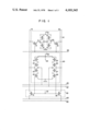
- FIG. 1 is a circuit diagram showing part of a semiconductor memory device according to an embodiment of the invention.
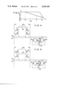
- FIGS. 2 and 3 show graphs illustrating the access time for each memory cell of the device shown in FIG. 1 together with that for an equivalent conventional device in the cases where aluminum gate type IG FETs and polycrystalline silicon gate type IG FETs are used, respectively;
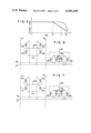
- FIGS. 4 to 7 each show a modified one of the data detection circuit used in the device shown in FIG. 1.
- FIG. 1 shows part of a semiconductor memory device having memory cells arranged in the form of a matrix and a data detection circuit disposed for each column. Though in FIG. 1, for a better understanding of the device, only one memory cell 10 is shown, memory cells similar to the memory cell 10 are actually disposed in a matrix form and a data detection circuit similar to the data detection circuit 20 is arranged for each column.
- the memory cell 10 has a p channel type IG FET 11 and n channel type IG FET 12 connected in series between a power source terminal V D1 and ground, and a p channel type IG FET 13 and n channel type IG FET 14 similarly connected in series therebetween.
- the connection point p1 between the IG FETs 11 and 12 is connected to respective gate electrodes of the IG FETs 13 and 14, and the connection point p2 between the IG FETs 13 and 14 is connected to respective gate electrodes of the IG FETs 11 and 12, thereby to constitute a flip-flop.
- the memory cell 10 further has an n channel type IG FET 15 connected between a data line 41 and the connection point p1 and an n channel type IG FET 16 connected between a data line 42 and the connection point p2. Respective gate electrodes of the IG FETs 15 and 16 are connected to a row selection line 43.
- a switching circuit 30 has n channel type IG FETs 31 and 32 for connecting the data lines 41 and 42 to data input lines 44 and 45, respectively, and a drive terminal 33 for receiving a column selection signal S from a column selection circuit (not shown). Respective gate electrodes of the IG FETs 31 and 32 are connected to the drive terminal 33.
- the data input lines 44 and 45 are adapted to transmit a data signal and an inverted signal of this data signal from data source (not shown), respectively.
- the data detection circuit 20 has p channel type IG FETs 21 and 22 and n channel type IG FETs 23 and 24, connected in series between a power source terminal V D2 and ground, and p channel type IG FETs 25 and 26 and n channel type IG FETs 27 and 28 connected in series between the power source terminal V D2 and ground, and a drive terminal 29 for receiving an inverted signal S of a column selection signal from the column selection circuit.
- the drive terminal 29 is connected to respective gate electrodes of the IG FETs 21 and 25, and the gate electrodes of the IG FETs 24 and 28 are connected to the drive terminal 33.
- a row selection line 43 is excited by a row selection circuit (not shown) and simultaneously the column selection signal S is applied from the column selection circuit (not shown) to the drive terminal 33.
- the IG FETs 31 and 32 are rendered conducting, so that data signals on the data input lines 44 and 45 are transmitted onto the data lines 41 and 42, respectively.
- the IG FETs 15 and 16 of the memory cell 10 are rendered conducting by the above excited row selection line 43. Assume now that a data signal on the data line 41 has a "1" level and a data signal on the data line 42 has a "0" level.
- the "1" level signal on the data line 41 is applied to the respective gate electrodes of the IG FETs 13 and 14 through the conducting IG FET 15, thereby rendering the IG FET 14 conducting and the IG FET 13 nonconducting
- the "0" level signal on the data line 42 is applied to the respective gate electrodes of the IG FETs 11 and 12 through the conducting IG FET 16, thereby rendering the IG FET 11 conducting and the IG FET 12 nonconducting.
- the point p1 is kept at a "1" level
- the point p2 is kept at a "0" level.
- a column selection signal is applied to the respective gate electrodes of the IG FETs 24 and 28 of the data detection circuit 20 through the drive terminal 33 of the switching circuit 30, thereby rendering the IG FETs 24 and 28 conducting, while an inverted signal of the column selection signal is applied to the respective gate electrodes of the IG FETs 21 and 25 through the drive terminal 29 of the detection circuit 20, thereby rendering the IG FETs 21 and 25 conducting.
- the signal on the data line 41 has a "1" level
- the IG FET 22 is kept nonconducting and the IG FET 23 is rendered conducting.
- the IG FET 26 is rendered conducting and the IG FET 27 is kept nonconducting.
- the inverted signals of the data signals on the data input lines 44 and 45 are transmitted onto the data output lines 46 and 47, respectively.
- the row selection line 43 is excited, and simultaneously a column selection signal and an inverted signal of the column selection signal are applied to the drive terminals 33 and 29, respectively.
- the data signal from the point p1 of the memory cell 10 which has a logical level of, for example, "1" is applied to the gate electrode of the IG FET 23 through the IG FET 15 and data line 41 to render the IG FET 23 conducting
- the data signal from the point p2 which has a logical level of "0” is applied to the gate electrode of the IG FET 26 through the IG FET 16 and data line 42 to render the IG FET 26 conducting.
- a "0" level signal and a "1" level signal are transmitted onto the data output lines 46 and 47, respectively.
- the data signal read from the memory cell is transmitted without being passed serially through an IG FET, it is free from a back gate bias effect unlike the conventional case, so that access time is decreased largely.
- FIGS. 2 and 3 show by solid lines, the variations in voltages on the data lines in reading a "0" level signal from the memory cell 10 in the case of constructing the semiconductor memory device shown in FIG. 1 by using IG FETs each having an aluminium gate and those each having a monocrystalline gate respectively.
- the broken lines indicate the variations in voltages on the data lines of a conventional equivalent semiconductor memory device.
- the data lines 41 and 42 are compulsively so excited as to have a "1" level signal.
- the "0" level data signal from the memory cell 10 is connected to the data line, and the signal level on this data line gradually decreases and at a point of time t1 the detection circuit 20 reads the signal on that data line as a data signal having a logical level of "0".
- the access time of the latter device was shortened by about 300 nanoseconds.
- the access time t1 of the present device is made largely shorter than the access time t2 of the conventional one.
- FIGS. 4 to 7 show respectively modified ones of the data detection circuit of the semiconductor memory device shown in FIG. 1.
- the data detection circuit shown in FIG. 4 includes p channel type IG FETs 121 and 122 connected in series between a power source terminal V D3 and a data output line 46, and p channel type IG FETs 123 and 124 connected in series between the power source terminal V D3 and a data output line 47. Respective gate electrodes of the IG FETs 121 and 123 are connected to a drive terminal 129 for receiving a column selection signal S, while respective gate electrodes of the IG FETs 122 and 124 are connected to the data lines 41 and 42, respectively.
- the data detection circuit further includes n channel type IG FETs 125 and 126 respectively provided between the data output lines 46, 47 and ground so as to maintain the data output lines 46 and 47 usually at a logical level of "0".
- Respective gate electrodes of the IG FETs 125 and 126 are applied with an inverted signal C of a chip selection signal C through a drive terminal 130 and, during a period in which the chip selecting operation is not performed, the IG FETs 125 and 126 are rendered conducting thereby to set the potential of the data output lines 46, 47 at a logical level of "0".
- Connected in parallel to the IG FETs 125 and 126 are n channel type IG FETs 127 and 128 having a small mutual conductance, respectively.
- the IG FETs 127 and 128 are applied with a voltage through a terminal V D4 at their respective gate electrodes and rendered always conducting to compensate that portion of the charge in the data output lines 46 and 47 which has leaked during the column selecting operation.
- the IG FETs 121 and 123 are rendered conducting.
- the IG FET 122 is not rendered conducting and accordingly the signal on the data output line 46 remains at a "0" level.
- the IG FET 124 is rendered conducting upon receipt of the "0" level signal on the data line 42, so that the signal level on the data output line 47 is altered to a "1" level by the power source terminal V D3 .
- the "1" and "0" level data signals on the data lines 41 and 42 are read on the data output lines 46 and 47 as "0" and "1" level data signals, respectively.
- the data detection circuit shown in FIG. 4 is constituted by the elements fewer in number than those constituting the data detection circuit of FIG. 1. Namely, in the data detection circuit of FIG. 1, an n ⁇ 8 number of elements are required for the memory cells arranged in the form of a matrix having n columns, whereas in the data detection circuit of FIG. 4 only an (n ⁇ 4 + 4) number of elements are required for the memory cells arranged in the n-column matrix.
- the circuit shown in FIG. 5 which is constructed by making the interchanges between the IG FETs 121 and 123 and between the IG FETs 121 and 123 and between the IG FETs 122 and 124, of the data detection circuit shown in FIG. 4 performs the same function as in the case of the data detection circuit of FIG. 4.
- n channel type IG FETs 221 and 222 and n channel type IG FETs 223 and 224 are connected in series between the data output lines 46, 47 and ground, respectively.
- Respective gate electrodes of IG FETs 221 and 223 are connected to the data lines 41 and 42, respectively, and respective gate electrodes of IG FETs 222 and 224 are connected to a drive terminal 229 for receiving a column selection signal.
- IG FETs 225 and 226 respectively connected between a power source terminal V D5 and the data output lines 46, 47. Respective gate electrodes of the IG FETs 225 and 226 are applied with a chip selection signal C through a drive terminal 230, and during a period in which the chip selecting operation is not carried out the IG FETs 225 and 226 are rendered conducting, so that the data output lines 46 and 47 are so excited through the power source terminal V D5 as to have a potential of "1" level.
- Connected in parallel to the IG FETs 225 and 226 are p channel type IG FETs 227 and 228 having a small mutual conductance, respectively.
- the IG FETs 227 and 228 have their respective gate electrodes kept at a ground potential and are rendered always conducting to compensate that portion of the charge in the data output lines 46 and 47 which has leaked during the chip selecting operation.
- the data detection circuit shown in FIG. 6 operates in accordance with the same principle, and has the same function and effect, as in the case of the circuit shown in FIG. 4. Further, the data detection circuit shown in FIG. 7 which is constructed by making the interchanges between the IG FETs 221 and 223 and between the IG FETs 222 and 224, of the data detection circuit of FIG. 6 functions in the same manner as in the case of the circuit of FIG. 6.
- This invention has above been explained by describing one embodiment, but is not limited thereto.
- the data detection circuits shown in FIGS. 1 and 4 to 7 it is possible to omit the IG FETs connected to one of the data lines 41 and 42, for example, the IG FETs 25, 26, 27 and 28, and omit the corresponding output line, for example, the data output line 47.
- the IG FETs 127, 128, 227 and 228 having a small mutual conductance may be omitted.
- the drive terminal 229 shown in FIGS. 6 and 7 may be connected to the drive terminal 33 of the switching circuit 30 shown in FIG. 1.
- FIG. 1 it is possible to perform the respective interchanges between the IG FETs 21, 24, 25 and 28 and the IG FETs 22, 23, 26 and 27.
Landscapes
- Engineering & Computer Science (AREA)
- Microelectronics & Electronic Packaging (AREA)
- Computer Hardware Design (AREA)
- Dram (AREA)
- Static Random-Access Memory (AREA)
Applications Claiming Priority (4)
| Application Number | Priority Date | Filing Date | Title |
|---|---|---|---|
| JP50050792A JPS51127628A (en) | 1975-04-28 | 1975-04-28 | Semiconductor memory |
| JP50/50792 | 1975-04-28 | ||
| JP50/144522 | 1975-12-03 | ||
| JP50144522A JPS5818711B2 (ja) | 1975-12-03 | 1975-12-03 | ハンドウタイキオクソウチノ デンアツセンスカイロ |
Publications (1)
| Publication Number | Publication Date |
|---|---|
| US4103345A true US4103345A (en) | 1978-07-25 |
Family
ID=26391263
Family Applications (1)
| Application Number | Title | Priority Date | Filing Date |
|---|---|---|---|
| US05/680,236 Expired - Lifetime US4103345A (en) | 1975-04-28 | 1976-04-26 | Semiconductor memory with data detection circuit |
Country Status (5)
| Country | Link |
|---|---|
| US (1) | US4103345A (show.php) |
| DE (1) | DE2618760C3 (show.php) |
| FR (1) | FR2309953A1 (show.php) |
| GB (1) | GB1522753A (show.php) |
| MY (1) | MY8100312A (show.php) |
Cited By (6)
| Publication number | Priority date | Publication date | Assignee | Title |
|---|---|---|---|---|
| US4479202A (en) * | 1979-09-13 | 1984-10-23 | Tokyo Shibaura Denki Kabushiki Kaisha | CMOS Sense amplifier |
| DE3419670A1 (de) * | 1983-05-26 | 1985-01-10 | Kabushiki Kaisha Toshiba, Kawasaki, Kanagawa | Halbleiter-speichereinrichtung |
| US4625298A (en) * | 1983-09-14 | 1986-11-25 | Mitsubishi Denki Kabushiki Kaisha | Semiconductor memory device |
| US4744063A (en) * | 1983-05-31 | 1988-05-10 | Kabushiki Kaisha Toshiba | Static memory utilizing transition detectors to reduce power consumption |
| EP0490690A1 (en) * | 1990-12-13 | 1992-06-17 | Mitsubishi Denki Kabushiki Kaisha | Amplifier circuit |
| DE4105268A1 (de) * | 1990-12-12 | 1992-06-17 | Samsung Electronics Co Ltd | Differentieller leseverstaerker |
Citations (6)
| Publication number | Priority date | Publication date | Assignee | Title |
|---|---|---|---|---|
| US3720922A (en) * | 1971-03-17 | 1973-03-13 | Rca Corp | Charge coupled memory |
| US3778782A (en) * | 1971-07-12 | 1973-12-11 | Texas Instruments Inc | Igfet dynamic address decode circuit |
| US3838295A (en) * | 1973-02-05 | 1974-09-24 | Lockheed Electronics Co | Ratioless mos sense amplifier |
| US3964031A (en) * | 1975-05-05 | 1976-06-15 | Rca Corporation | Memory cell |
| US3980899A (en) * | 1974-10-30 | 1976-09-14 | Hitachi, Ltd. | Word line driver circuit in memory circuit |
| US4045785A (en) * | 1975-11-05 | 1977-08-30 | American Microsystems, Inc. | Sense amplifier for static memory device |
-
1976
- 1976-04-26 US US05/680,236 patent/US4103345A/en not_active Expired - Lifetime
- 1976-04-28 DE DE2618760A patent/DE2618760C3/de not_active Expired
- 1976-04-28 GB GB17236/76A patent/GB1522753A/en not_active Expired
- 1976-04-28 FR FR7612595A patent/FR2309953A1/fr active Granted
-
1981
- 1981-12-31 MY MY1981312A patent/MY8100312A/xx unknown
Patent Citations (6)
| Publication number | Priority date | Publication date | Assignee | Title |
|---|---|---|---|---|
| US3720922A (en) * | 1971-03-17 | 1973-03-13 | Rca Corp | Charge coupled memory |
| US3778782A (en) * | 1971-07-12 | 1973-12-11 | Texas Instruments Inc | Igfet dynamic address decode circuit |
| US3838295A (en) * | 1973-02-05 | 1974-09-24 | Lockheed Electronics Co | Ratioless mos sense amplifier |
| US3980899A (en) * | 1974-10-30 | 1976-09-14 | Hitachi, Ltd. | Word line driver circuit in memory circuit |
| US3964031A (en) * | 1975-05-05 | 1976-06-15 | Rca Corporation | Memory cell |
| US4045785A (en) * | 1975-11-05 | 1977-08-30 | American Microsystems, Inc. | Sense amplifier for static memory device |
Cited By (8)
| Publication number | Priority date | Publication date | Assignee | Title |
|---|---|---|---|---|
| US4479202A (en) * | 1979-09-13 | 1984-10-23 | Tokyo Shibaura Denki Kabushiki Kaisha | CMOS Sense amplifier |
| DE3419670A1 (de) * | 1983-05-26 | 1985-01-10 | Kabushiki Kaisha Toshiba, Kawasaki, Kanagawa | Halbleiter-speichereinrichtung |
| US4916665A (en) * | 1983-05-26 | 1990-04-10 | Kabushiki Kaisha Toshiba | Semiconductor memory device with P-channel MOS transistor load circuit |
| US4744063A (en) * | 1983-05-31 | 1988-05-10 | Kabushiki Kaisha Toshiba | Static memory utilizing transition detectors to reduce power consumption |
| US4625298A (en) * | 1983-09-14 | 1986-11-25 | Mitsubishi Denki Kabushiki Kaisha | Semiconductor memory device |
| DE4105268A1 (de) * | 1990-12-12 | 1992-06-17 | Samsung Electronics Co Ltd | Differentieller leseverstaerker |
| EP0490690A1 (en) * | 1990-12-13 | 1992-06-17 | Mitsubishi Denki Kabushiki Kaisha | Amplifier circuit |
| US5248946A (en) * | 1990-12-13 | 1993-09-28 | Mitsubishi Denki Kabushiki Kaisha | Symmetrical differential amplifier circuit |
Also Published As
| Publication number | Publication date |
|---|---|
| DE2618760A1 (de) | 1976-11-04 |
| DE2618760C3 (de) | 1978-11-30 |
| FR2309953B1 (show.php) | 1981-12-04 |
| GB1522753A (en) | 1978-08-31 |
| FR2309953A1 (fr) | 1976-11-26 |
| MY8100312A (en) | 1981-12-31 |
| DE2618760B2 (de) | 1978-04-06 |
Similar Documents
| Publication | Publication Date | Title |
|---|---|---|
| US4247791A (en) | CMOS Memory sense amplifier | |
| KR930000712B1 (ko) | 반도체 집적회로 | |
| US4575825A (en) | Semiconductor memory device | |
| US4893278A (en) | Semiconductor memory device including precharge/equalization circuitry for the complementary data lines | |
| US5479369A (en) | Semiconductor integrated circuit device and semiconductor memory device | |
| KR930002253B1 (ko) | Mos 스태틱형 ram | |
| US4174541A (en) | Bipolar monolithic integrated circuit memory with standby power enable | |
| KR850004855A (ko) | 반도체 메모리 장치 | |
| US4031415A (en) | Address buffer circuit for semiconductor memory | |
| US4159540A (en) | Memory array address buffer with level shifting | |
| US4000429A (en) | Semiconductor circuit device | |
| US3990056A (en) | High speed memory cell | |
| EP0085436B1 (en) | Buffer circuits | |
| US4103345A (en) | Semiconductor memory with data detection circuit | |
| US3875567A (en) | Memory circuit using variable threshold level field-effect device | |
| US3733591A (en) | Non-volatile memory element | |
| US4091461A (en) | High-speed memory cell with dual purpose data bus | |
| US4918657A (en) | Semiconductor memory device provided with an improved precharge and enable control circuit | |
| GB2172761A (en) | Sense amplifier for semiconductor ram | |
| JPS5831679B2 (ja) | モノリシック集積回路 | |
| US4802126A (en) | Semiconductor memory device | |
| EP0350860A2 (en) | Semiconductor memory having improved sense amplifiers | |
| JPH05120881A (ja) | 半導体記憶装置 | |
| EP0317963A2 (en) | Semiconductor memory device having dRAM cells | |
| JPH11306761A (ja) | データ入出力回路、半導体記憶装置および情報処理装置 |