US3953733A - Method of operating imagers - Google Patents
Method of operating imagers Download PDFInfo
- Publication number
- US3953733A US3953733A US05/579,690 US57969075A US3953733A US 3953733 A US3953733 A US 3953733A US 57969075 A US57969075 A US 57969075A US 3953733 A US3953733 A US 3953733A
- Authority
- US
- United States
- Prior art keywords
- during
- voltage
- location
- storage means
- time
- Prior art date
- Legal status (The legal status is an assumption and is not a legal conclusion. Google has not performed a legal analysis and makes no representation as to the accuracy of the status listed.)
- Expired - Lifetime
Links
Images


Classifications
-
- H—ELECTRICITY
- H10—SEMICONDUCTOR DEVICES; ELECTRIC SOLID-STATE DEVICES NOT OTHERWISE PROVIDED FOR
- H10F—INORGANIC SEMICONDUCTOR DEVICES SENSITIVE TO INFRARED RADIATION, LIGHT, ELECTROMAGNETIC RADIATION OF SHORTER WAVELENGTH OR CORPUSCULAR RADIATION
- H10F39/00—Integrated devices, or assemblies of multiple devices, comprising at least one element covered by group H10F30/00, e.g. radiation detectors comprising photodiode arrays
- H10F39/10—Integrated devices
- H10F39/12—Image sensors
- H10F39/15—Charge-coupled device [CCD] image sensors
- H10F39/158—Charge-coupled device [CCD] image sensors having arrangements for blooming suppression
-
- H—ELECTRICITY
- H04—ELECTRIC COMMUNICATION TECHNIQUE
- H04N—PICTORIAL COMMUNICATION, e.g. TELEVISION
- H04N25/00—Circuitry of solid-state image sensors [SSIS]; Control thereof
- H04N25/50—Control of the SSIS exposure
- H04N25/57—Control of the dynamic range
- H04N25/571—Control of the dynamic range involving a non-linear response
-
- H—ELECTRICITY
- H04—ELECTRIC COMMUNICATION TECHNIQUE
- H04N—PICTORIAL COMMUNICATION, e.g. TELEVISION
- H04N25/00—Circuitry of solid-state image sensors [SSIS]; Control thereof
- H04N25/60—Noise processing, e.g. detecting, correcting, reducing or removing noise
- H04N25/63—Noise processing, e.g. detecting, correcting, reducing or removing noise applied to dark current
-
- H—ELECTRICITY
- H04—ELECTRIC COMMUNICATION TECHNIQUE
- H04N—PICTORIAL COMMUNICATION, e.g. TELEVISION
- H04N25/00—Circuitry of solid-state image sensors [SSIS]; Control thereof
- H04N25/60—Noise processing, e.g. detecting, correcting, reducing or removing noise
- H04N25/67—Noise processing, e.g. detecting, correcting, reducing or removing noise applied to fixed-pattern noise, e.g. non-uniformity of response
-
- H—ELECTRICITY
- H04—ELECTRIC COMMUNICATION TECHNIQUE
- H04N—PICTORIAL COMMUNICATION, e.g. TELEVISION
- H04N25/00—Circuitry of solid-state image sensors [SSIS]; Control thereof
- H04N25/60—Noise processing, e.g. detecting, correcting, reducing or removing noise
- H04N25/68—Noise processing, e.g. detecting, correcting, reducing or removing noise applied to defects
-
- H—ELECTRICITY
- H04—ELECTRIC COMMUNICATION TECHNIQUE
- H04N—PICTORIAL COMMUNICATION, e.g. TELEVISION
- H04N25/00—Circuitry of solid-state image sensors [SSIS]; Control thereof
- H04N25/70—SSIS architectures; Circuits associated therewith
- H04N25/71—Charge-coupled device [CCD] sensors; Charge-transfer registers specially adapted for CCD sensors
- H04N25/713—Transfer or readout registers; Split readout registers or multiple readout registers
-
- H—ELECTRICITY
- H04—ELECTRIC COMMUNICATION TECHNIQUE
- H04N—PICTORIAL COMMUNICATION, e.g. TELEVISION
- H04N25/00—Circuitry of solid-state image sensors [SSIS]; Control thereof
- H04N25/70—SSIS architectures; Circuits associated therewith
- H04N25/71—Charge-coupled device [CCD] sensors; Charge-transfer registers specially adapted for CCD sensors
- H04N25/745—Circuitry for generating timing or clock signals
-
- H—ELECTRICITY
- H10—SEMICONDUCTOR DEVICES; ELECTRIC SOLID-STATE DEVICES NOT OTHERWISE PROVIDED FOR
- H10D—INORGANIC ELECTRIC SEMICONDUCTOR DEVICES
- H10D44/00—Charge transfer devices
- H10D44/40—Charge-coupled devices [CCD]
- H10D44/45—Charge-coupled devices [CCD] having field effect produced by insulated gate electrodes
- H10D44/472—Surface-channel CCD
- H10D44/476—Three-phase CCD
Definitions
- the present invention relates to methods of operating imagers such as (CCD) imagers.
- Improved performance is achieved by changing during the integration time, the capacity of the charge storage means at each location of the imager.
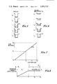
- FIG. 1 is a section through a CCD channel of a three-phase imager and illustrates also the substrate surface potential profile during the integration time;
- FIG. 2 is a drawing of waveforms to help explain the operation of the imager of FIG. 1;
- FIG. 3 is a graph of dark current as a function of the voltage applied to a transfer electrode
- FIG. 4 is a drawing of the waveform employed to obtain the improved operation discussed in the present application.
- FIG. 5 is a drawing of a potential well beneath a charge accumulation electrode during successive times in an integration interval, when that electrode is maintained at a fixed potential, as is done in the known art;
- FIG. 6 is a drawing showing the operation under the same conditions as in FIG. 5 but using the mode of operation suggested herein;
- FIG. 7 is a graph of scene brightness verses position under an assumed set of circumstances
- FIG. 8 is a graph illustrating the video output obtained at successive locations along one row of an imager under the conditions of FIG. 7;
- FIG. 9 is a drawing of waveforms to illustrate how dynamic range can be increased.
- FIG. 10 illustrates the same variables as FIG. 8 but obtained using the waveforms of FIG. 9;
- FIGS. 11-13 and 17 show other waveforms which may be employed to increase dynamic range and FIG. 13 also shows a waveform which may be employed for gamma correction;
- FIG. 14 is a plot of brightness verses drive signal amplitude for a kinescope
- FIG. 15 shows the output of a CCD camera which in one case is corrected for gamma and in another case, is uncorrected;
- FIG. 16 is a section transverse of a CCD channel of an imager and illustrates also certain substrate surface potential profiles during the integration time.
- the CCD imager shown includes a P-type substrate 10 and a plurality of electrodes insulated from and capacitively coupled to the substrate.
- the showing is schematic in the sense that the insulation employed, which is normally silicone dioxide, is not shown specifically and the electrode structure is shown only schematically.
- the type of CCD chosen for illustration is a three phase device and in a practical circuit, the electrodes may overlap one another or may be side-by-side, as shown with, for example, insulation in the gaps between electrodes.
- the present invention is applicable also to two or four or higher phase structures which are not illustrated specifically.
- the substrate may be of N-type rather than P-type, provided supply voltages are chosen of appropriate polarity.
- the structure shown in FIG. 1 may be assumed to constitute a portion of one vertical channel of the image sensing region of the array, sometimes also known as the A register.
- one of the electrodes of each stage (the ⁇ 2 electrodes in the example) may be maintained at a fixed voltage level to cause depletion regions to form beneath such electrodes and the remaining electrodes, namely the ⁇ 1 and ⁇ 3 electrodes, may be maintained at potentials such as to maintain the substrate regions beneath these electrodes in mild depletion or in slight accumulation. This is illustrated at a in FIG. 1.
- two electrodes of each stage may be maintained at a potential to form deep depletion regions and the third at a potential to maintain the substrate in mild depletion or in slight accumulation.
- the heavily depleted regions form potential wells in the substrate, that is, they form regions at the substrate surface from which majority carriers (holes) have been repelled and where minority carrier surface charge (electrons) may accumulate.
- the lightly depleted (or mildly accumulated) regions of the substrate form potential barriers between the potential wells.
- a radiation image is applied to the imager either through the electrodes, as illlustrated schematically, or through the back surface of the substrate. (It may be assumed for purposes of the present discussion that, if front surface illumination is employed, the electrodes are substantially transparent to the radiation.) Charges accumulate in the various potential wells in accordance with the radiation intensity reaching the substrate in the region close to the respective ⁇ 2 electrode locations. As illustrated in FIG. 1(a), the radiation intensity in the region of electrode 12 is greater than that in the region of electrode 14 so that more charge carriers accumulate in potential well 12a than in potential well 14a.
- the charge carriers in the example illustrated are electrons.
- FIG. 2 illustrates the waveforms which are employed.
- the ⁇ 2 voltage is at a fixed level such that depletion regions are formed.
- the ⁇ 1 and ⁇ 3 electrodes are at a fixed lever and in the present illustration that level is such that the regions of the substrate beneath these electrodes are in mild accumulation. It is advantageous to operate in this way to achieve what is known as "operational blooming control.”
- the ⁇ 1 and ⁇ 3 voltage levels may be somewhat higher (more positive) such that the regions of the substrates beneath these electrodes are in mild depeletion.
- the integration time may be relatively long, somewhat under 1/60'th of a second in the case of commercial television.
- the charges stored in the imager are transferred to a so called B register (a temporary storage array) and from the B register transferred a row at a time to a C register.
- the transfer of charge from the A to the B register is accomplished by the multiple phase voltages shown during the vertical retrace period which may be some 900 microseconds or so.
- dark current defects refers to a location or locations of the imager which generates substantial numbers of charge carriers, even in the absence of radiation excitation. In normal operation such defects appear as intense white spots in the reproduced picture. It is believed that such defects are a result of the thermal generation of charge carriers.
- dark currents produced are extremely sensitive to the amplitude of the applied electric field and this, in turn, is proportional to the voltage applied to the electrodes during the integration time.
- the graph of FIG. 3 illustrates this.
- the dark current legended "normal background current”
- the dark current varies with applied voltage as shown by the solid line curve A.
- the dark current varies with voltage in the manner shown by solid line curve B. Note the exponential increase in dark current with applied voltage.
- a voltage is applied which starts at a low level and which increases as a function of time in a manner to cause the substrate potential to increase linearly with time.
- the voltage itself is illustrated as a linear ramp; however, it is to be understood that it may, in practice, be slightly non-linear to the extent required by the substrate doping employed.
- Such a wave is shown in FIG. 4 by the solid line 20.
- the previously known way of operating is illustrated by the dot dash line 22.
- the area under the solid curve B is only about one third that under the dashed curve BB and indeed it has been shown empirically that this kind of improvement is achieved.
- the test was made using a three phase CCD imager having 256 by 160 locations and operated with the regions between potential wells in light depletion during the integration time. During this test it was found that the resolution and potential well size were unaffected by the use a ramp voltage. There was a small decrease in sensitivity to light, probably due to a decrease in the average size of the depletion region. This should only be a second order effect for imagers with long carrier diffusion length compared with depletion size.
- FIG. 6 illustrates the performance obtained employing a linear ramp during the integration time as shown in FIG. 4. While at time t 0 , for example, the size of the well is considerably smaller (shallower) than in the prior art, the amount of charge signal which has to be accumulated also is relatively small. Accordingly, it can be accumulated even in this shallow well. However, at the relatively low voltage involved, not much dark current is generated, even if a defect is present, as is clear from FIG. 3. As time passes, more and more charge becomes available but the depth of the well also increases with time.
- the well size can be made always to be adequate to accommodate the charge which is being generated, and as the higher voltages are employed for only a relatively smaller portion of the integration time than in the prior art, the dark currents generated at defective locations are considerably smaller than in the prior art.
- FIGS. 7 and 8 illustrate another problem which may occur during the operation of a CCD imager in the conventional way, that is, with the waveforms shown in FIGS. 2 and 3.
- FIG. 7 is a plot of scene brightness verses position in the scene, for an assumed image along one direction of an array.
- the scene brightness is assumed to increase linearly as a function of position.
- At some arbitrary position x 2 there is perturbation in the brightness level, shown as a sudden decrease in brightness.
- the excess charge carriers will combine with the majority carriers present under the ⁇ 1 and ⁇ 3 electrodes and be disposed of in this way (assuming that operational blooming control is being employed as illustrated in FIG. 2).
- structural blooming control buses may be employed for removing the excess charge to prevent blooming.
- the dynamic range of the imager may be greatly improved (increased) in accordance with a second aspect of the invention by operating in the way illustrated in FIG. 9.
- the ⁇ 1 and ⁇ 3 voltages are similar to the corresponding voltages of FIG. 2.
- the ⁇ 2 voltage is different.
- the ⁇ 2 voltage is at one level V 1 and during the remainder T 2 of the integration time, the ⁇ 2 voltage is at a second, higher level V 2 .
- the dashed line 52 corresponds to the curve of FIG. 8. It represents the amplitude of the video output V O as a function of brightness level for the case in which the ⁇ 2 voltage is at a constant level V 2 for the entire integration time.
- the dashed line 54 shows the video output voltage V O which would be obtained if the ⁇ 2 electrodes were held at a constant level V 1 for the portion T 1 of the integration time.
- the slope of curve 54 is proportional to the fraction T 1 /(T 1 +T 2 ). That is, the greater the fraction of the integration time occupied by T 1 , the closer will be the slope of the ramp portion of curve 54 to that of 52.
- the slope indicates the number of charge carriers which will be collected at a location, in response to a given brightness level, during the entire period T 1 .
- the greater T 1 of course, the greater the number of carriers collected, at a given brightness level.
- some number of carriers C 1 will be collected during T 1 (curve 54) and during the total time T 1 + T 2 , a greater number of carriers C 2 would be collected.
- Curve 55 illustrates the video output obtained by operating the ⁇ 2 gate electrodes at the potential V 2 for the relatively short period T 2 .
- the slope of this curve is proportional to T 2 /(T 1 +T 2 ) and the saturation level is V S2 . It may be observed that saturation in this particular example is not obtained except at extremely high brightness levels (they would be off scale). Of course, this is an example only as the inventive teachings are applicable to longer time periods than shown for T 2 (or shorter ones, if desired).
- the solid line curve 56 shows the performance obtained using the two level waveform shown in FIG. 9. It is obtained by adding curve 55 to curve 54.
- V 0 is obtained which is proportional to this brightness. Any brightness level would tend to produce a video level greater than V S1 during the integration time T 1 , causes saturation of a potential well and the excess charge is removed in the manner already described.
- the potential wells are made deeper by changing the voltage V 1 to V 2 . This immediately terminates any blooming which may be present. And it permits the accumulation of additional charge carriers in the potential wells for the relatively short interval T 2 .
- the integrating voltage ⁇ 2 consists of two linear ramps of difference slopes S 1 and S 2 .
- the wave of FIG. 12 has only two ramps, it is possible instead to use three, four or more ramps of successively increasing slopes rather than the two shown.
- FIGS. 14 and 15 illustrate yet another problem which may be dealt with according to the methods of the present invention.
- the display brightness is not linearly proportional to the kinescope drive signal amplitude. Rather, it varies in non-linear fashion, as shown.
- An imager such as a CCD imager produces outputs linearly proportional to the scene being imaged (assuming operation below blooming levels). It is possible to gamma correct the video signal obtained in the same way that video signals obtained from conventional tube type television cameras such as vidicons or plumbicons are gamma corrected. When this is done it results in amplifying the dimmer parts of the scene which include low level inherent noise components. Such low level signal variations, when amplified, appear larger relative to the larger amplitude signals derived from the brighter parts of the scene. Unfortunately, however, certain noise components such as the fixed pattern noise due to spatial variations in background dark current level are greater (at room temperature) in a CCD produced signal than, for example, in a signal produced by a plumbicon.
- gamma correction can be obtained "on chip" during the integration time by employing an appropriate integration waveform ⁇ 2 .
- a waveform is illustrated by dashed curve 60 in FIG. 13.
- the ⁇ 2 voltage varies in non-linear fashion to cause a corresponding variation in depth of the potential wells beneath the ⁇ 2 electrodes.
- the result is relative accentuation of the low level signals and attenuation of the higher level signals.
- dynamic range is improved in the manner already discussed.
- the price paid, as compared to operating at a constant integration voltage, is that more light is needed.
- the camera aperture must be opened wider than if a constant voltage such as V 2 is employed.
- the wave 58 need not start at as high a level as illustrated but instead may be closer to wave 60. This would decrease the light requirements.
- partial gamma compensation may be obtained on chip (say correction to 0.7) and the remainder of the correction achieved by external, conventional gamma compensation circuits.
- on chip gamma correction as discussed above is very important in color cameras. The reason is that it is necessary that red, blue and green color components add properly over all brightness levels. Such on chip gamma correction can be achieved in the manner already discussed, for each of the three imagers employed for the three different colors.
- CCD imagers While the techniques discussed herein are especially useful in CCD imagers, they may also be employed in other forms of imagers such as those employing photodiodes and blooming buses, those employing "charge injection” devices, and even tube type imagers such as silicon vidicons. These techniques are applicable to self-scanned as well as x-y addressed imagers.
- FIG. 16 This FIGURE is a section transverse of the channel direction, the channel extending into the page.
- the structure shown in FIG. 16 includes a P-type substrate 80, a drain for charge carriers in the substrate, shown as an N-type diffusion 82, and electrodes 84, 86 and 88 over the substrate and insulated therefrom.
- electrode 86 is held at a fixed level such as V 2 .
- electrode 84 is maintained at a relatively lower level to produce a blooming barrier 89 of the height illustrated at (a) in FIG. 16. The effect of doing this is to reduce the effective depth of the potential well to D 1 as illustrated in FIG. 16. Any excess charge carriers due to an intense image, overflow this barrier and pass to the drain diffusion 82.
- the voltage V BB is decreased (made less positive) to increase the height of the blooming barrier 89 as shown at (b) in FIG. 16 and in this way to increase the effective depth of the potential well from D 1 to D 2 .
- the operation obtained is substantially the same as that discussed previously in connection with FIG. 9 even though ⁇ 2 is kept at a constant level during the entire integration time in FIG. 16.
- the electrode 88 illustrated in FIG. 16 is for the purpose of providing a so called "channel stop," that is, a potential barrier 90 for confining the charge to the channel.
- a channel stop that is, a potential barrier 90 for confining the charge to the channel.
- Alternative structures such as a P-type diffusion which is more heavily doped than the P-type substrate, could of course, be used instead to provide a suitable channel stop.
- FIG. 17 illustrates yet another way for increasing the dynamic range (and is applicable also to gamma correction).
- the ⁇ 2 voltage is at a level V 1 such as to create deep depletion regions beneath the ⁇ 2 electrodes.
- the ⁇ 2 voltage is decreased to a level V 1 . If any excess charge is present in the resulting depletion regions of reduced size, that excess charge will flow to the regions of the substrate in accumulation, assuming operational blooming control as illustrated in FIG. 2. (Alternatively, structural blooming control buses could be employed.) The effect therefore is the same as would be obtained if, during the period t 0 to t 2 , the voltage were at the constant level V 1 .
- the ⁇ 2 voltage returns to its initial value V 1 and then at time t 3 the voltage goes to level V 2 which is higher than V 1 . Again, any excess charge which may be present due to the reduced size of the depletion region will flow to the regions of the substrate in accumulation. The effect is the same as if, during the period t 2 to t 4 , the voltage were at the level V 2 .
- FIG. 17 also may be employed for gamma correction. This may be done by choosing appropriate values of V 1 , V 2 and V 3 and appropriate points during the integration time during which these voltage levels are to be applied. The objective, of course, is to simulate a smooth curve such as 60 of FIG. 13. While only three notches are shown in FIG. 17, a more faithful simulation can be obtained if more than this number of notches is employed.
- the duration of periods such as t 1 and t 2 can be of the order of a millisecond or so; however, this time is not critical.
Landscapes
- Engineering & Computer Science (AREA)
- Multimedia (AREA)
- Signal Processing (AREA)
- Physics & Mathematics (AREA)
- Nonlinear Science (AREA)
- Transforming Light Signals Into Electric Signals (AREA)
- Solid State Image Pick-Up Elements (AREA)
Priority Applications (8)
| Application Number | Priority Date | Filing Date | Title |
|---|---|---|---|
| US05/579,690 US3953733A (en) | 1975-05-21 | 1975-05-21 | Method of operating imagers |
| GB20713/76A GB1531920A (en) | 1975-05-21 | 1976-05-19 | Methods of operating imagers |
| NLAANVRAGE7605367,A NL188261C (nl) | 1975-05-21 | 1976-05-20 | Besturingsinrichting voor een beeldopnemer. |
| FR7615278A FR2312147A1 (fr) | 1975-05-21 | 1976-05-20 | Procede de mise en oeuvre d'un capteur d'images a couplage de charge |
| CA252,988A CA1103346A (en) | 1975-05-21 | 1976-05-20 | Methods of operating imagers |
| IT23461/76A IT1060656B (it) | 1975-05-21 | 1976-05-20 | Metodo di funzionamento di un dispositivo per la formazione di immagini |
| JP51058987A JPS51142908A (en) | 1975-05-21 | 1976-05-20 | Method of operating picture device |
| DE2622828A DE2622828C3 (de) | 1975-05-21 | 1976-05-21 | Verfahren zum Betreiben von BiIdfühlern |
Applications Claiming Priority (1)
| Application Number | Priority Date | Filing Date | Title |
|---|---|---|---|
| US05/579,690 US3953733A (en) | 1975-05-21 | 1975-05-21 | Method of operating imagers |
Publications (1)
| Publication Number | Publication Date |
|---|---|
| US3953733A true US3953733A (en) | 1976-04-27 |
Family
ID=24317943
Family Applications (1)
| Application Number | Title | Priority Date | Filing Date |
|---|---|---|---|
| US05/579,690 Expired - Lifetime US3953733A (en) | 1975-05-21 | 1975-05-21 | Method of operating imagers |
Country Status (8)
| Country | Link |
|---|---|
| US (1) | US3953733A (en:Method) |
| JP (1) | JPS51142908A (en:Method) |
| CA (1) | CA1103346A (en:Method) |
| DE (1) | DE2622828C3 (en:Method) |
| FR (1) | FR2312147A1 (en:Method) |
| GB (1) | GB1531920A (en:Method) |
| IT (1) | IT1060656B (en:Method) |
| NL (1) | NL188261C (en:Method) |
Cited By (33)
| Publication number | Priority date | Publication date | Assignee | Title |
|---|---|---|---|---|
| DE2842346A1 (de) * | 1977-09-29 | 1979-04-12 | Sony Corp | Bildabtaster in festkoerpertechnik |
| US4314275A (en) * | 1980-03-24 | 1982-02-02 | Texas Instruments Incorporated | Infrared time delay with integration CTD imager |
| WO1983000267A1 (en) * | 1981-07-06 | 1983-01-20 | Takeshita, Kaneyoshi | Solid state image pickup device |
| US4377755A (en) * | 1980-07-15 | 1983-03-22 | The United States Of America As Represented By The Secretary Of The Air Force | Signal compressor apparatus |
| FR2537813A1 (fr) * | 1982-12-10 | 1984-06-15 | Thomson Csf | Procede de reglage des conditions de fonctionnement d'un dispositif photosensible a transfert de charge et dispositif pour sa mise en oeuvre |
| US4598414A (en) * | 1981-12-18 | 1986-07-01 | Honeywell Inc. | Input compression apparatus for charge coupled devices |
| US4845566A (en) * | 1986-05-21 | 1989-07-04 | Canon Kabushiki Kaisha | Solid-state image pickup apparatus having controllable means for eliminating surplus charge |
| US4926247A (en) * | 1986-10-15 | 1990-05-15 | Olympus Optical Co., Ltd. | Color imaging apparatus including a means for electronically non-linearly expanding and compressing dynamic range of an image signal |
| US5008758A (en) * | 1989-05-24 | 1991-04-16 | Massachusetts Institute Of Technology | Suppressing dark current in charge-coupled devices |
| FR2668608A1 (fr) * | 1990-06-21 | 1992-04-30 | Loral Fairchild Corp | Non-linear photosite response in ccd imagers. |
| EP0484135A3 (en) * | 1990-11-01 | 1992-09-23 | Canon Kabushiki Kaisha | Image sensing apparatus having tone control function |
| WO1992022091A1 (en) * | 1991-06-07 | 1992-12-10 | Eastman Kodak Company | Enhanced exposure latitude of image sensor having lateral overflow drain |
| US5426515A (en) * | 1992-06-01 | 1995-06-20 | Eastman Kodak Company | Lateral overflow gate driver circuit for linear CCD sensor |
| US5602407A (en) * | 1994-05-31 | 1997-02-11 | Dalsa, Inc. | Switched CCD electrode photodetector |
| US5642163A (en) * | 1994-08-31 | 1997-06-24 | Matsushita Electric Industrial Co., Ltd. | Imaging apparatus for switching the accumulative electric charge of an image pickup device |
| WO1998056006A1 (en) * | 1997-06-02 | 1998-12-10 | Sarnoff Corporation | Extended dynamic range imaging system and method |
| WO2000046981A1 (en) * | 1999-02-02 | 2000-08-10 | Ball Aerospace & Technologies Corp. | Method and apparatus for enhancing the dynamic range of a ccd sensor |
| US20010010548A1 (en) * | 2000-02-02 | 2001-08-02 | Minolta Co., Ltd. | Image-sensing device |
| US6472653B1 (en) * | 1999-03-22 | 2002-10-29 | Sarnoff Corporation | Method and apparatus to extend dynamic range of time delay and integrate charge coupled devices |
| EP0991128A3 (en) * | 1998-09-25 | 2004-02-04 | Lockheed Martin Corporation | Dynamic range extension of CCD imagers |
| US20050083421A1 (en) * | 2003-10-16 | 2005-04-21 | Vladimir Berezin | Dynamic range enlargement in CMOS image sensors |
| US20050206760A1 (en) * | 2004-03-17 | 2005-09-22 | Sanyo Electric Co., Ltd. | Voltage controller and voltage control method for charge-coupled device |
| US20050212936A1 (en) * | 2004-03-25 | 2005-09-29 | Eastman Kodak Company | Extended dynamic range image sensor with fixed pattern noise reduction |
| US20060022113A1 (en) * | 2004-07-27 | 2006-02-02 | Tower John R | Imaging methods and apparatus having extended dynamic range |
| US20060022223A1 (en) * | 2004-05-10 | 2006-02-02 | Tetsuro Kumesawa | Solid state imaging device |
| US20060082670A1 (en) * | 2004-10-14 | 2006-04-20 | Eastman Kodak Company | Interline CCD for still and video photography with extended dynamic range |
| KR100639155B1 (ko) * | 1997-06-02 | 2006-10-27 | 사르노프 코포레이션 | 영상 시스템의 동적 범위를 확장하기 위한 시스템 및 방법 |
| US7265397B1 (en) | 2000-08-30 | 2007-09-04 | Sarnoff Corporation | CCD imager constructed with CMOS fabrication techniques and back illuminated imager with improved light capture |
| US20080198246A1 (en) * | 2007-02-16 | 2008-08-21 | Photon Dynamics, Inc. | Sensor-based gamma correction of a digital camera |
| US20110073982A1 (en) * | 2007-05-25 | 2011-03-31 | Armstrong J Joseph | Inspection system using back side illuminated linear sensor |
| EP2230831B1 (en) * | 2009-03-17 | 2018-10-31 | E2V Technologies (UK) Limited | CCD imaging array with extended dynamic range |
| US10257448B1 (en) | 2015-08-18 | 2019-04-09 | Sri International | Extended dynamic range imaging sensor and operating mode of the same |
| US10827139B2 (en) | 2015-08-18 | 2020-11-03 | Sri International | Multiple window, multiple mode image sensor |
Families Citing this family (4)
| Publication number | Priority date | Publication date | Assignee | Title |
|---|---|---|---|---|
| JPS538015A (en) * | 1976-07-12 | 1978-01-25 | Toshiba Corp | Pick up system with charge coupled element |
| JPS55163882A (en) * | 1979-06-06 | 1980-12-20 | Nec Corp | System for driving charge transfer element |
| EP0033129B1 (en) * | 1980-01-25 | 1984-06-13 | Kabushiki Kaisha Toshiba | Charge transfer apparatus |
| US5742297A (en) * | 1994-11-04 | 1998-04-21 | Lockheed Martin Corporation | Apparatus and method for constructing a mosaic of data |
Citations (2)
| Publication number | Priority date | Publication date | Assignee | Title |
|---|---|---|---|---|
| US3845295A (en) * | 1973-05-02 | 1974-10-29 | Rca Corp | Charge-coupled radiation sensing circuit with charge skim-off and reset |
| US3883437A (en) * | 1974-01-25 | 1975-05-13 | Hughes Aircraft Co | Monolithic IR detector arrays with direct injection charge coupled device readout |
Family Cites Families (2)
| Publication number | Priority date | Publication date | Assignee | Title |
|---|---|---|---|---|
| JPS5721904B2 (en:Method) * | 1973-10-03 | 1982-05-10 | ||
| JPS5339211B2 (en:Method) * | 1973-10-26 | 1978-10-20 |
-
1975
- 1975-05-21 US US05/579,690 patent/US3953733A/en not_active Expired - Lifetime
-
1976
- 1976-05-19 GB GB20713/76A patent/GB1531920A/en not_active Expired
- 1976-05-20 CA CA252,988A patent/CA1103346A/en not_active Expired
- 1976-05-20 NL NLAANVRAGE7605367,A patent/NL188261C/xx not_active IP Right Cessation
- 1976-05-20 IT IT23461/76A patent/IT1060656B/it active
- 1976-05-20 JP JP51058987A patent/JPS51142908A/ja active Pending
- 1976-05-20 FR FR7615278A patent/FR2312147A1/fr active Granted
- 1976-05-21 DE DE2622828A patent/DE2622828C3/de not_active Expired
Patent Citations (2)
| Publication number | Priority date | Publication date | Assignee | Title |
|---|---|---|---|---|
| US3845295A (en) * | 1973-05-02 | 1974-10-29 | Rca Corp | Charge-coupled radiation sensing circuit with charge skim-off and reset |
| US3883437A (en) * | 1974-01-25 | 1975-05-13 | Hughes Aircraft Co | Monolithic IR detector arrays with direct injection charge coupled device readout |
Cited By (51)
| Publication number | Priority date | Publication date | Assignee | Title |
|---|---|---|---|---|
| DE2842346A1 (de) * | 1977-09-29 | 1979-04-12 | Sony Corp | Bildabtaster in festkoerpertechnik |
| FR2409646A1 (fr) * | 1977-09-29 | 1979-06-15 | Sony Corp | Detecteur d'image en technique etat solide |
| US4314275A (en) * | 1980-03-24 | 1982-02-02 | Texas Instruments Incorporated | Infrared time delay with integration CTD imager |
| US4377755A (en) * | 1980-07-15 | 1983-03-22 | The United States Of America As Represented By The Secretary Of The Air Force | Signal compressor apparatus |
| WO1983000267A1 (en) * | 1981-07-06 | 1983-01-20 | Takeshita, Kaneyoshi | Solid state image pickup device |
| US4598414A (en) * | 1981-12-18 | 1986-07-01 | Honeywell Inc. | Input compression apparatus for charge coupled devices |
| FR2537813A1 (fr) * | 1982-12-10 | 1984-06-15 | Thomson Csf | Procede de reglage des conditions de fonctionnement d'un dispositif photosensible a transfert de charge et dispositif pour sa mise en oeuvre |
| US4845566A (en) * | 1986-05-21 | 1989-07-04 | Canon Kabushiki Kaisha | Solid-state image pickup apparatus having controllable means for eliminating surplus charge |
| US4926247A (en) * | 1986-10-15 | 1990-05-15 | Olympus Optical Co., Ltd. | Color imaging apparatus including a means for electronically non-linearly expanding and compressing dynamic range of an image signal |
| US5008758A (en) * | 1989-05-24 | 1991-04-16 | Massachusetts Institute Of Technology | Suppressing dark current in charge-coupled devices |
| FR2668608A1 (fr) * | 1990-06-21 | 1992-04-30 | Loral Fairchild Corp | Non-linear photosite response in ccd imagers. |
| US5406391A (en) * | 1990-11-01 | 1995-04-11 | Canon Kabushiki Kaisha | Image sensing apparatus having tone control function |
| EP0484135A3 (en) * | 1990-11-01 | 1992-09-23 | Canon Kabushiki Kaisha | Image sensing apparatus having tone control function |
| US5295001A (en) * | 1990-11-01 | 1994-03-15 | Canon Kabushiki Kaisha | Image sensing apparatus having tone control function |
| WO1992022091A1 (en) * | 1991-06-07 | 1992-12-10 | Eastman Kodak Company | Enhanced exposure latitude of image sensor having lateral overflow drain |
| US5426515A (en) * | 1992-06-01 | 1995-06-20 | Eastman Kodak Company | Lateral overflow gate driver circuit for linear CCD sensor |
| US5602407A (en) * | 1994-05-31 | 1997-02-11 | Dalsa, Inc. | Switched CCD electrode photodetector |
| US5642163A (en) * | 1994-08-31 | 1997-06-24 | Matsushita Electric Industrial Co., Ltd. | Imaging apparatus for switching the accumulative electric charge of an image pickup device |
| WO1998056006A1 (en) * | 1997-06-02 | 1998-12-10 | Sarnoff Corporation | Extended dynamic range imaging system and method |
| US6101294A (en) * | 1997-06-02 | 2000-08-08 | Sarnoff Corporation | Extended dynamic imaging system and method |
| KR100639155B1 (ko) * | 1997-06-02 | 2006-10-27 | 사르노프 코포레이션 | 영상 시스템의 동적 범위를 확장하기 위한 시스템 및 방법 |
| US7020353B1 (en) * | 1997-06-02 | 2006-03-28 | Sarnoff Corporation | Extended dynamic range imaging system and method |
| EP0991128A3 (en) * | 1998-09-25 | 2004-02-04 | Lockheed Martin Corporation | Dynamic range extension of CCD imagers |
| WO2000046981A1 (en) * | 1999-02-02 | 2000-08-10 | Ball Aerospace & Technologies Corp. | Method and apparatus for enhancing the dynamic range of a ccd sensor |
| US6188433B1 (en) | 1999-02-02 | 2001-02-13 | Ball Aerospace & Technologies Corp. | Method and apparatus for enhancing the dynamic range of a CCD sensor |
| US6472653B1 (en) * | 1999-03-22 | 2002-10-29 | Sarnoff Corporation | Method and apparatus to extend dynamic range of time delay and integrate charge coupled devices |
| US20010010548A1 (en) * | 2000-02-02 | 2001-08-02 | Minolta Co., Ltd. | Image-sensing device |
| US7236192B2 (en) | 2000-02-02 | 2007-06-26 | Minolta Co., Ltd. | Image-sensing device |
| US7265397B1 (en) | 2000-08-30 | 2007-09-04 | Sarnoff Corporation | CCD imager constructed with CMOS fabrication techniques and back illuminated imager with improved light capture |
| US20050083421A1 (en) * | 2003-10-16 | 2005-04-21 | Vladimir Berezin | Dynamic range enlargement in CMOS image sensors |
| US20050206760A1 (en) * | 2004-03-17 | 2005-09-22 | Sanyo Electric Co., Ltd. | Voltage controller and voltage control method for charge-coupled device |
| US20050212936A1 (en) * | 2004-03-25 | 2005-09-29 | Eastman Kodak Company | Extended dynamic range image sensor with fixed pattern noise reduction |
| WO2005096620A1 (en) | 2004-03-25 | 2005-10-13 | Eastman Kodak Company | Extended dynamic range image sensor |
| EP2365691A1 (en) | 2004-03-25 | 2011-09-14 | Eastman Kodak Company | Extended dynamic range image method |
| US20060022223A1 (en) * | 2004-05-10 | 2006-02-02 | Tetsuro Kumesawa | Solid state imaging device |
| US20060022113A1 (en) * | 2004-07-27 | 2006-02-02 | Tower John R | Imaging methods and apparatus having extended dynamic range |
| US7378634B2 (en) | 2004-07-27 | 2008-05-27 | Sarnoff Corporation | Imaging methods and apparatus having extended dynamic range |
| US7709863B2 (en) * | 2004-10-05 | 2010-05-04 | Sony Corporation | Solid state imaging device |
| US8426896B2 (en) | 2004-10-05 | 2013-04-23 | Sony Corporation | Solid state imaging device |
| US20100165159A1 (en) * | 2004-10-05 | 2010-07-01 | Sony Corporation | Solid state imaging device |
| US20110163361A1 (en) * | 2004-10-05 | 2011-07-07 | Sony Corporation | Solid state imaging device |
| US7977710B2 (en) | 2004-10-05 | 2011-07-12 | Sony Corporation | Solid state imaging device |
| US8115236B2 (en) | 2004-10-05 | 2012-02-14 | Sony Corporation | Solid state imaging device |
| US20060082670A1 (en) * | 2004-10-14 | 2006-04-20 | Eastman Kodak Company | Interline CCD for still and video photography with extended dynamic range |
| US7796171B2 (en) * | 2007-02-16 | 2010-09-14 | Flir Advanced Imaging Systems, Inc. | Sensor-based gamma correction of a digital camera |
| US20080198246A1 (en) * | 2007-02-16 | 2008-08-21 | Photon Dynamics, Inc. | Sensor-based gamma correction of a digital camera |
| US20110073982A1 (en) * | 2007-05-25 | 2011-03-31 | Armstrong J Joseph | Inspection system using back side illuminated linear sensor |
| EP2230831B1 (en) * | 2009-03-17 | 2018-10-31 | E2V Technologies (UK) Limited | CCD imaging array with extended dynamic range |
| US10257448B1 (en) | 2015-08-18 | 2019-04-09 | Sri International | Extended dynamic range imaging sensor and operating mode of the same |
| US10535690B1 (en) | 2015-08-18 | 2020-01-14 | Sri International | Extended dynamic range imaging sensor and operating mode of the same |
| US10827139B2 (en) | 2015-08-18 | 2020-11-03 | Sri International | Multiple window, multiple mode image sensor |
Also Published As
| Publication number | Publication date |
|---|---|
| FR2312147A1 (fr) | 1976-12-17 |
| DE2622828C3 (de) | 1978-07-13 |
| CA1103346A (en) | 1981-06-16 |
| FR2312147B1 (en:Method) | 1982-05-28 |
| IT1060656B (it) | 1982-08-20 |
| JPS51142908A (en) | 1976-12-08 |
| NL188261B (nl) | 1991-12-02 |
| NL7605367A (nl) | 1976-11-23 |
| DE2622828A1 (de) | 1976-12-02 |
| NL188261C (nl) | 1992-05-06 |
| DE2622828B2 (de) | 1977-12-01 |
| GB1531920A (en) | 1978-11-15 |
Similar Documents
| Publication | Publication Date | Title |
|---|---|---|
| US3953733A (en) | Method of operating imagers | |
| US4032976A (en) | Smear reduction in ccd imagers | |
| CA1049122A (en) | Blooming control for charge coupled imager | |
| US4322753A (en) | Smear and/or blooming in a solid state charge transfer image pickup device | |
| US4780764A (en) | Image sensing apparatus | |
| US4242599A (en) | Charge transfer image sensor with antiblooming and exposure control | |
| US20040046879A1 (en) | Solid state image pickup apparatus | |
| US4774585A (en) | Image pickup apparatus | |
| US4450484A (en) | Solid states image sensor array having circuit for suppressing image blooming and smear | |
| JPH10304256A (ja) | Ccdイメージャ | |
| JPH10505724A (ja) | Ccdイメージャの動作方法及び当該方法の実施に適するccdイメージャ | |
| US6180935B1 (en) | Dynamic range extension of CCD imagers | |
| US5923370A (en) | Image smear and dark signal reduction device and method | |
| US6778214B1 (en) | Charge generation of solid state image pickup device | |
| JPS6369267A (ja) | 固体撮像装置の駆動方法 | |
| KR100255531B1 (ko) | 고체 촬상 장치 및 구동 방법 | |
| CA1193711A (en) | Solid state image sensor | |
| US4845566A (en) | Solid-state image pickup apparatus having controllable means for eliminating surplus charge | |
| EP0022323B1 (en) | Solid-state imaging device | |
| JPH05137072A (ja) | 固体撮像装置 | |
| US4794279A (en) | A solid state imaging device which applies two separate storage voltages for the signal charges so as to reduce the smear level and the dark current | |
| US10911703B2 (en) | Image sensor and control method thereof, and image capturing apparatus with event counters and reverse bias voltages | |
| US6778215B1 (en) | Driving method of solid-state image pickup device and image pickup system | |
| US7365786B2 (en) | Solid state image sensing apparatus with enhanced sensitivity realized by improving linear characteristic of photodiode and its driving method | |
| EP0346905B1 (en) | Electronic shutter controlling method for a two-dimensional charge-coupled device |