US5923370A - Image smear and dark signal reduction device and method - Google Patents
Image smear and dark signal reduction device and method Download PDFInfo
- Publication number
- US5923370A US5923370A US08/726,827 US72682796A US5923370A US 5923370 A US5923370 A US 5923370A US 72682796 A US72682796 A US 72682796A US 5923370 A US5923370 A US 5923370A
- Authority
- US
- United States
- Prior art keywords
- storage
- interline
- clocking
- register
- isolation
- Prior art date
- Legal status (The legal status is an assumption and is not a legal conclusion. Google has not performed a legal analysis and makes no representation as to the accuracy of the status listed.)
- Expired - Lifetime
Links
- 230000009467 reduction Effects 0.000 title claims description 18
- 238000000034 method Methods 0.000 title claims description 17
- 238000012546 transfer Methods 0.000 claims abstract description 106
- 238000003384 imaging method Methods 0.000 claims abstract description 67
- 229910021420 polycrystalline silicon Inorganic materials 0.000 claims abstract description 19
- 229910052751 metal Inorganic materials 0.000 claims abstract description 11
- 239000002184 metal Substances 0.000 claims abstract description 11
- 238000002955 isolation Methods 0.000 claims description 81
- 230000010354 integration Effects 0.000 claims description 40
- 238000007599 discharging Methods 0.000 claims 3
- 238000001444 catalytic combustion detection Methods 0.000 description 58
- XUIMIQQOPSSXEZ-UHFFFAOYSA-N Silicon Chemical compound [Si] XUIMIQQOPSSXEZ-UHFFFAOYSA-N 0.000 description 16
- 229910052710 silicon Inorganic materials 0.000 description 16
- 239000010703 silicon Substances 0.000 description 16
- 238000010586 diagram Methods 0.000 description 12
- 230000003287 optical effect Effects 0.000 description 11
- 229920005591 polysilicon Polymers 0.000 description 11
- 239000000758 substrate Substances 0.000 description 7
- 229910052782 aluminium Inorganic materials 0.000 description 6
- XAGFODPZIPBFFR-UHFFFAOYSA-N aluminium Chemical compound [Al] XAGFODPZIPBFFR-UHFFFAOYSA-N 0.000 description 6
- 238000013461 design Methods 0.000 description 6
- 238000005516 engineering process Methods 0.000 description 6
- 210000004027 cell Anatomy 0.000 description 4
- 230000008030 elimination Effects 0.000 description 4
- 238000003379 elimination reaction Methods 0.000 description 4
- 238000012545 processing Methods 0.000 description 4
- 230000004888 barrier function Effects 0.000 description 3
- 239000013078 crystal Substances 0.000 description 3
- 230000005865 ionizing radiation Effects 0.000 description 3
- 239000000463 material Substances 0.000 description 3
- 230000008569 process Effects 0.000 description 2
- 230000005855 radiation Effects 0.000 description 2
- 230000003068 static effect Effects 0.000 description 2
- 238000009825 accumulation Methods 0.000 description 1
- 230000004075 alteration Effects 0.000 description 1
- 238000003491 array Methods 0.000 description 1
- 239000000969 carrier Substances 0.000 description 1
- 230000015556 catabolic process Effects 0.000 description 1
- 230000008859 change Effects 0.000 description 1
- 238000010276 construction Methods 0.000 description 1
- 230000007547 defect Effects 0.000 description 1
- 238000006731 degradation reaction Methods 0.000 description 1
- 230000001419 dependent effect Effects 0.000 description 1
- 230000003292 diminished effect Effects 0.000 description 1
- 238000006073 displacement reaction Methods 0.000 description 1
- 230000000694 effects Effects 0.000 description 1
- 238000007667 floating Methods 0.000 description 1
- 230000006872 improvement Effects 0.000 description 1
- 238000002347 injection Methods 0.000 description 1
- 239000007924 injection Substances 0.000 description 1
- 239000012212 insulator Substances 0.000 description 1
- 230000007246 mechanism Effects 0.000 description 1
- 238000012986 modification Methods 0.000 description 1
- 230000004048 modification Effects 0.000 description 1
- 150000004767 nitrides Chemical class 0.000 description 1
- 230000001151 other effect Effects 0.000 description 1
- 239000002245 particle Substances 0.000 description 1
- 238000005036 potential barrier Methods 0.000 description 1
- 229920006395 saturated elastomer Polymers 0.000 description 1
- 230000035945 sensitivity Effects 0.000 description 1
- 238000009416 shuttering Methods 0.000 description 1
- 239000007858 starting material Substances 0.000 description 1
- 210000000352 storage cell Anatomy 0.000 description 1
- 230000000007 visual effect Effects 0.000 description 1
Images


Classifications
-
- H—ELECTRICITY
- H04—ELECTRIC COMMUNICATION TECHNIQUE
- H04N—PICTORIAL COMMUNICATION, e.g. TELEVISION
- H04N25/00—Circuitry of solid-state image sensors [SSIS]; Control thereof
- H04N25/70—SSIS architectures; Circuits associated therewith
- H04N25/71—Charge-coupled device [CCD] sensors; Charge-transfer registers specially adapted for CCD sensors
- H04N25/715—Charge-coupled device [CCD] sensors; Charge-transfer registers specially adapted for CCD sensors using frame interline transfer [FIT]
-
- H—ELECTRICITY
- H04—ELECTRIC COMMUNICATION TECHNIQUE
- H04N—PICTORIAL COMMUNICATION, e.g. TELEVISION
- H04N25/00—Circuitry of solid-state image sensors [SSIS]; Control thereof
- H04N25/60—Noise processing, e.g. detecting, correcting, reducing or removing noise
- H04N25/62—Detection or reduction of noise due to excess charges produced by the exposure, e.g. smear, blooming, ghost image, crosstalk or leakage between pixels
- H04N25/625—Detection or reduction of noise due to excess charges produced by the exposure, e.g. smear, blooming, ghost image, crosstalk or leakage between pixels for the control of smear
-
- H—ELECTRICITY
- H04—ELECTRIC COMMUNICATION TECHNIQUE
- H04N—PICTORIAL COMMUNICATION, e.g. TELEVISION
- H04N25/00—Circuitry of solid-state image sensors [SSIS]; Control thereof
- H04N25/60—Noise processing, e.g. detecting, correcting, reducing or removing noise
- H04N25/63—Noise processing, e.g. detecting, correcting, reducing or removing noise applied to dark current
Definitions
- the invention relates generally to charge coupled device image sensors and specifically to methods of improving sensor performance by smear signal and dark current signal reduction.
- CCDs Charge couple devices
- the architecture of CCD video sensors generally follow the form dictated by the National Television Standards Committee (NTSC) for video broadcast standards.
- CCD video sensor designs need at least 488 TV lines vertically, 500 to 800 pixels per TV line, have an optical format of 4/3 aspect ratio, and generated field interlaced video at a frame rate of 30 Hz.
- CCD architectures which achieved the goals of the video format imaging requirements generally fell into two categories: Interline Transfer (ILT) or Frame Transfer (FT) image sensors.
- Other types of video sensors have also been developed such as full frame (FF), MOS X-Y, and charge injection devices (CID).
- This invention relates mainly to the ILT and FT image sensors and has little or no relevance to the other forms of video format image sensors.
- Frame transfer sensors rely on the integration of an odd or even field of data, the quick transfer of that image field data to an optically opaque analog storage array, and the subsequent parallel to serial transfer of the video data to a camera circuit.
- An optically opaque storage array is a storage array that is covered by an optically opaque material such as an aluminum film so that the storage array is not photo-sensitive.
- the rapid vertical transfer of the image data from integration of the first video field is vital since the optical input onto the imaging section of the CCD sensor is continuous (not strobed or modulated during transfer). However, since vertical transfer requires a finite time to complete, there is always some fraction of image signal from subsequent integration fields collected in the vertical shift register during the field transfer to the storage region.
- the quantity of signal charge present in the video field which results from integration during the transfer time is said to be a smear signal offset to the proper video signal.
- Each pixel collects a fraction of the image charge as it rapidly passes through the image while transferring to the storage area.
- the quantity of smear is measured as a fraction of the nominal signal level and is proportional to the transfer time and the local optical power density.
- the visual effect of the smear charge, as it appears on a video monitor, is a vertical strip of excess brightness emanating from the bright source in the image. The stripe may be faint or saturated depending on the brightness of the source.
- Interline transfer CCD image sensors solved the problem of transferring a field of image data during the integration of the next field of data by using an opaque vertical shift register (i.e., a shift register covered by an opaque material).
- the opaque vertical shift resigster is disposed adjacent to the photosensitive pixel. Signals from one field of pixels is very rapidly transferred to the vertical register and then transferred in a parallel/serial manner at the normal (60 Hz) field rate. The majority of the smear content is thus eliminated since the image data from the preceding field is shielded by the opaque film disposed over the vertical shift register from further integration during the readout even though the entire array is illuminated with the optical signal from the image plane.
- the penalty for this improved smear function is the reduction in optical aperture of the individual imaging pixel (by approximately 50%). Thus, the sensitivity of the sensor is diminished by 50%. Additionally, the ILT employs a relatively slow parallel to serial readout rate corresponding to 244 vertical lines read out in 1/60 sec. Even though the vertical readout registers are most likely shielded from a direct optical signal, the small amount of optical signal which "leaks" (e.g., via a phenomenon known as light piping) into the vertical register during vertical field transfer has substantial integration time to build up unwanted smear signal.
- CCD image sensor pixel structures and processes have been continuously improved such that commercially available CCD image sensors used in both consumer camcorders and broadcast video systems have reduced smear content to -90 dB below the nominal signal level. Improved smear performance is realized by several techniques described herein and are used in the current embodiment of the invention.
- the present invention further improves on the prior art by applying very fast frame transfer techniques and very fast smear signal reset structures to reduce the smear signal content by an additional -20 dB to -30 dB. This smear reduction is accomplished while maintaining optimum optical aperture, signal charge saturation, antiblooming protection, electronic shuttering, and transfer characteristics for the CCD video image sensor.
- CCD imaging devices which are comprised of combinations of interline transfer and frame transfer technologies (called frame interline transfer or FIT) have been reported.
- frame interline transfer or FIT interline transfer
- Such devices have been developed for the proposed HDTV video applications which involve larger, higher resolution arrays, higher data rates, smaller pixel dimensions, and different video signal formats to those of the standard RS170 video format.
- the prior art applied to HDTV format image sensors does in fact reduce smear signal by quickly clearing the image charge from the vertical interline shift registers into the light shielded frame storage registers.
- the current invention describes a CCD video image sensor device architecture which demonstrates an improvement over the prior art (FIT) for smear signal reduction.
- CCD image sensors experience thermally generated leakage currents which integrates the potential wells of the CCD shift register.
- the leakage current results in a background signal level known in the industry as dark current and is usually specified as a current density in nanoamps per square centimeter.
- the dark current is generated by both surface state and bulk traps or defects in the crystal and typically generate signal carriers (electrons in most CCD's) with a rate which doubles for every 7 degrees C in temperature change.
- the dark current density at 53 C is 16 nA/cm2.
- the dark current density is a characteristic of the silicon process and the device structure and may be lowered by reduction of bulk and surface generation sites.
- Dark current density which has been established by the CCD processing can be reduced during the CCD operation by employing a clocking scheme for the CCD electrodes known in the industry as multi-pinned phase (MPP) operation.
- MPP multi-pinned phase
- surface state related dark current electrons are recombined with holes pulled to the surface from the p-type regions adjacent to the CCD channels.
- dark current can be minimized to values as low as 0.01 nA/cm2 at 25 C. This value is still finite and non-zero and still is subject to the same doubling rate as the operating temperature of the device increases.
- the dark current signal increases the dynamic range or contrast ratio of the CCD sensor is reduced, which reduces the overall system performance.
- CCD device performance parameter is radiation tolerance.
- Ionizing radiation sources such as those found in vacuum space, can create damage to a CCD image sensor over the lifetime of the sensor.
- Mechanisms for this damage include generation of fixed oxide charge in gates and other insulator regions of the CCD sensor, silicon crystal displacement damage, as well as other effects. Crystal damage and surface state density alterations generally result in increased dark current density and reduced charge transfer efficiency over time. Fixed oxide charge results in threshold shifts, educed amplifier performance, and reduced charge transfer efficiency.
- a CCD image sensor designed for the purpose of real time video imaging is generally described as an interlace format interline transfer (ILT) or frame transfer (FT) area imaging device.
- ILT interlace format interline transfer
- FT frame transfer
- NTSC standards commonly known as RS170 video broadcast standards. These standards include specifications for image aspect ratio (4:3), number of video lines per picture height, interlacing scheme, and frequencies of operation.
- a CCD image sensor architecture which conforms to the RS170 video format comprises an interline transfer imaging architecture 11, a horizontal readout register 12, and an output amplifier structure 13.
- An alternative CCD video image sensor architecture is a frame transfer structure (FIG. 2) comprising a frame transfer imaging section 21, a field storage section 22, a horizontal readout register 23, and an output amplifier structure 24.
- the interline architecture (hereafter ILT architecture) includes an integration site or pixel 14, a pixel to vertical register transfer region 15, and a vertical transfer register 16. Visible radiation from the imaged scene is focused onto the imaging array 11, and falls on the pixel which is typically a form of silicon photodiode.
- the pixel may also be constructed of an MOS gated region using doped polysilicon material as a somewhat transparent electrode.
- the pixel aperture is usually defined by a patterned layer of aluminum. An aluminum layer covers the vertical shift register 16 and reflects the light incident at that location. Light falling on the open pixel is converted to electrons and holes in the silicon substrate. Electrons are collected in potential wells in the silicon substrate formed at the pixel.
- the charge from alternate pixels is transferred laterally to a receiving potential well in the vertical shift register. Electrons or signal charge from alternate pixels is transferred in alternate image fields corresponding to the NTSC television monitor scan sequence called interlacing. This transfer is affected by the application of a voltage to the MOS electrodes of the vertical shift register.
- the register electrodes have applied voltages in a clocked sequence such that the signal charge is transferred vertically downward in a line by line fashion.
- the signal charge is transferred to a horizontal CCD shift register 12 at the bottom of the array.
- the signal charge is transferred laterally in a serial fashion using voltages applied to the register electrodes in a clocked sequence.
- the signal charge is then converted to a voltage through a capacitive sense node and then the voltage signal is coupled to the external circuitry through a simple analog amplifier circuit 13.
- the parallel to serial transfer of a frame of image information is thus completed in an interlace field sequence with each field having one-half of the number of video lines.
- the time interval allowed for the sequence to be completed is set by the NTSC standards at 30 frames per second.
- the frame transfer CCD architecture (hereafter FT architecture) includes an imaging region 21, a field storage region 22, a horizontal readout register 23, and an output amplifier 24.
- the entire imaging region is photoactive and no overlaying aluminum or other light shielding area is defined in the pixel.
- the vertical registers are clocked at high speed into receiving register elements in the field storage section 22.
- the imaging section is then reset to a static potential.
- Alternate electrodes from those activated in the first integration are activated in the second field creating integration sites which are displaced by one pixel dimension vertically.
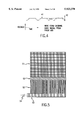
- FIG. 3A represents a frame of video imagery 31 with 488 lines of vertical resolution 32 and the corresponding video wave form signal generated at the output of the horizontal shift register.
- the number of horizontal resolution elements 35 is not established by NTSC standards but is typically 550 to 768 pixels per line.
- the graphic depicts imagery from a uniformly dark background with a bright target in the scene which is approximately 10% of the picture height.
- a video wave form 33 indicates the odd field voltage output wave form from the CCD image sensor.
- the video signal from the bright object for example an object located at line N 38, is at a value near to the peak output signal possible from the sensor.
- the region of video depicted as a white band running vertically is generally described as smear signal and results in unwanted signal in lines above and below the bright object in the scene 34.
- the amount of smear signal, shown at 37 of video line N 1 is measured from the reference level 36 (i.e., the dark background of the image that would otherwise be the signal corresponding to the particular pixel).
- the smear signal is usually specified as a fractional percentage of the nominal signal in the region of the bright object.
- the fractional value of smear signal can be as high as 10% to as little as 0.001% depending on the design of the image sensor pixel and readout structures.
- FIG. 3B depicts the same scene as shown in FIG. 3A with the image smear virtually eliminated.
- Video wave form 38 shows no measurable smear signal as is characteristic of the present invention.
- Dark signal 42 adding to background signal 41, is generated by several sources including surface state generation sites the oxide/silicon interface and bulk silicon generation sites.
- the control of dark current generation largely depends on the details of the silicon processing used as well as the purity of the bulk silicon starting material.
- the dark current generally results in unwanted background signal charge in the absence of optical input which can be viewed as point sources or collections of point sources in the image.
- the dark signal may also be seen as a largely uniform voltage offset of the video in the dark with gradual variations across the CCD sensor.
- CCD image sensors The generation sites for dark current in CCD image sensors generally follow a statistical thermal generation characteristic which predicts a doubling of dark current generation for every 7 degrees centigrade increase in substrate temperature.
- CCD image sensors are susceptible to reduction in dynamic range performance and a degradation of the signal to noise ratio when the sensor is subjected to elevated temperatures.
- dark current generation site density can be increased when the sensor is subjected to ionizing radiation sources such as X-rays and energetic charged particles such as electrons or protons.
- CCD image sensors can be subjected to ionizing radiation which increases the dark current generation site density gradually over the lifetime of the device.
- the invention improves the CCD video imaging technology by reducing the smear content and the dark current content in the imagery using a technique of rapid elimination of the unwanted signal charge during the blank period between the odd and even field readout sequences.
- the present invention the fast frame interline transfer (FFIT) CCD device, demonstrates the capability of simultaneously reducing smear signal and accumulated dark signal, beyond the capabilities of the prior art, through practicing the methods of the invention.
- FFIT fast frame interline transfer
- a fast frame interline transfer charge coupled device imaging sensor that includes an imaging section and an storage section.
- the imaging section includes a plurality of interline transfer registers, each interline transfer register containing a plurality of interline register elements.
- the imaging section further includes an interline clocking structure, the interline clocking structure including polycrystalline silicon buss lines used as gate electrodes, the polycrystalline silicon buss lines being connected to a metal strapping network, the interline clocking structure causing charge to be transferred between interline register elements of each interline transfer register based on interline clocking signals.
- the storage section is coupled to the imaging section.
- the storage section includes a plurality of storage registers, each storage register containing a plurality of storage register elements.
- the storage section further includes a storage discharge structure and a storage clocking structure.
- Each storage register element of the storage registers is selectively coupleable through the storage discharge structure to a storage drain.
- the storage clocking structure has first and second clocking structure parts, the first clocking structure part corresponding to first storage register elements coupled to respective interline registers.
- the first clocking structure part is coupled to the interline clocking structure so as to cause charge to be transferred from the respective interline registers to the first storage register elements based on the interline clocking signals.
- the second clocking structure part causes charge to be transferred between storage register elements of each storage register based on frame clocking signals.
- FIG. 1 is a block diagram of an interline transfer CCD video image sensor
- FIG. 2 is a block diagram of a frame transfer video image sensor
- FIGS. 3A and 3B are signal diagram representations of the presence and non-presence, respectively of smear on a video image
- FIG. 4 is a video wave form depicting a dark signal
- FIG. 5 is a block diagram of FFIT image sensor according to the present invention.
- FIGS. 6A-6E are potential well and timing diagrams depicting an imaging section according to the present invention.
- FIGS. 7A-7D are potential well and timing diagrams depicting storage and isolation sections of the present invention.
- FIG. 8 is a functional schematic diagram depicting image charge transfer with smear and dark signal elimination
- FIG. 9 is a schematic diagram of an embodiment of the present invention.
- FIG. 10 is a layout of an imaging pixel in the present invention.
- FIG. 11 is a layout of storage isolation cell in the present invention.
- FIG. 12 is a metal strapped CCD gate structure.
- a CCD video imaging device which includes an interline transfer pixel array 51, similar to that described with reference to FIG. 1, a field storage register 52, similar to that described with reference to FIG. 2, a horizontal readout register 53, an output amplifier 54, and a storage isolation section 55.
- this device is defined as a Frame Interline Transfer CCD imaging device (FIT).
- FIT Frame Interline Transfer CCD imaging device
- metal bus structures on the imaging and storage array renders the device capable of very high speed clocking of the vertical and storage register elements in a burst mode which is signified by the naming of the technology disclosed herein as Fast Frame Interline Transfer (FFIT) CCD image sensor technology.
- FFIT Fast Frame Interline Transfer
- the FIT CCD architecture has been successfully used to reduce smear in HDTV sensors to a value of -100 dB or 0.001% of the nominal signal output.
- the pixel design for the FIT sensor utilizes advanced device design and silicon processing capabilities to minimize the causes of image smear in an image sensor.
- FIGS. 6A-6E describe a cross section of the Fast Frame Interline Transfer pixel region with the potential wells appropriate for operation and coincident with the timing diagram included.
- the cross section of the interline transfer pixel (in the imaging section) is shown as a pinned photodiode 61, polysilicon gate electrode 62 over an insulating gate nitride/oxide, a metal light shield 63, implanted channel stops 64, a buried channel 65 (forming a part of a vertical shift register), a shallow p-tub 66. an antiblooming/exposure control (AB/EC) gate 67, and an N+ diode 68 connected to the AB/EC gate formed in a barrier region.
- the entire structure is fabricated on a p- epitaxial structure on a p+ silicon substrate.
- Incident optical energy or visible photons 69 from the image are focused onto the CCD image sensor and are absorbed in the bulk silicon region through the aperture defined by the aluminum light shield. Electrons 69.1 and holes are generated in the silicon bulk at various depths depending on the wavelength of the light. Electrons are collected in the potential wells capacitively established in the polysilicon gated regions and under the pinned photodiode region.
- FIG. 6B shows the potential in the silicon corresponding to the time interval t1 in FIG. 6E.
- the potential at the AB/EC junction and gate are held at a high potential relative to the adjacent pinned photodiode potential such that the electrons accumulated in the well 69.2 formed in the integration site are caused to be eliminated in the N+ diode drain.
- This condition created by applying anti-blooming voltage VAB (69.5 of FIG. 6E) to gate electrode 67, is described as being in exposure control mode where all the signal charge generated during the t1 period of time is drained away into diode 68.
- Smear charge 69.3 and dark signal charge 69.4 can accumulate during this period as well as during the integration period (shown in FIG. 6C during time t2).
- the smear charge is created by several means.
- One is the multiple reflection of incident light between the light shield and the silicon substrate. Electrons are generated and collected directly in the vertical shift register. This effect is known in the industry as light piping and can be responsible for a significant fraction of the smear charge generation.
- electrons which are generated deep in the substrate beyond the depletion regions of the formed potential wells are free to drift toward the nearest potential well. Some fraction of the drift electrons can be collected by the vertical shift register. The collection of the drift electrons is greatly reduced by the presence of a small potential barrier resulting from p-tub region surrounding the buried channel.
- signal charge is collected in the well defined by the pinned photodiode.
- Some fraction of the signal charge is collected directly by the vertical shift register as smear charge (and dark signal charge).
- the percentage of smear charge as a fraction of the image signal is defined by the pixel cross section and increases linearly with a decrease in integration time. This is because the smear signal (and dark signal) is generated at a constant rate independent of the integration time while the signal charge collected in the integration well is dependent on the fraction of time within the frame time that the pixel is in integration mode.
- the integration is complete and the transfer of signal charge from the pixel is commenced by applying clock voltage C1 (69.6 of FIG. 6E) to gate electrode 62.
- clock voltage C1 69.6 of FIG. 6E
- the signal charge from the image would then be added to the smear charge and dark signal already present in the vertical shift register.
- the present invention eliminates most of the accumulated smear and dark signal charge in the vertical shift register just prior to the time period t3 such that image signal charge is transferred to an empty vertical register well (e.g., 65 in FIG. 6A).
- the unwanted smear and dark signal charge is eliminated by rapidly clocking the vertical shift registers into the storage registers where the unwanted charge is drained through a gate controlled drain circuit in the storage cell.
- FIG. 7A a cross section of a storage and isolation register cell is depicted. It is formed with polysilicon gate electrodes 71 over CCD buried channel 72, bordered by a storage reset gate 73, and a drain diode 74.
- FIGS. 7B, 7C and 7D show how charge in the isolation and storage registers are drained of unwanted charge.
- the storage register well is enabled by applying no storage reset voltage (FIG. 7D) to reset gate 73 (FIG. 7A) while applying storage clock voltage (FIG. 7D) to gate electrode 71 (FIG. 7A) so that the barrier created at the reset gate is in the off (low voltage) mode.
- the barrier to the drain diode is eliminated by applying the storage reset voltage (FIG. 7D) to reset gate 73, and the charge in the storage register is drained.
- This drain sequence occurs during the short time interval just before the end of the integration period and before the transfer of charge from the pixels into the vertical shift registers.
- the unwanted smear charge is drained into the isolation and/or storage register drains such that there is no mixing of smear signal with the image signal.
- the dark signal which has accumulated during the integration period is also drained through the isolation and storage register drains.
- FIG. 8 illustrates the movement of signal, smear, and dark current charges during the integration and rapid elimination of the unwanted signal charges. Desired signal charge 81 from the image is collected in the pixel integration site 82. A fraction of the signal charge is lost to the vertical shift register 83 as smear charge 84. Additionally, dark signal charge 85 is being accumulated in the vertical shift register. The combined smear charge and dark signal charge 86 is rapidly transferred down to the isolation storage registers 87 as undesired smear and dark signal charge 86. There the storage register reset gate 88 is held high and the smear and dark current charge from the vertical registers are drained into the n+ diode 89. Additionally, the dark signal 89.1 accumulated in the isolation storage register 87 is eliminated through the lateral storage drain structure 88, 89.
- the design of the vertical shift register of the ILT pixel region incorporates a metal strapped CCD gate structure 120 (FIG. 12).
- the metal strapping 122, 124 of the polysilicon gate buss structures 103A, 103B dramatically reduces the resistive load on the clock drivers and shortens the RC time constant of the vertical register such that the vertical register clocks may be operated, in a burst mode, at greater than 10 MHz.
- the entire 244 lines per field may be rapidly transferred to the isolation storage registers (e.g. 55 of FIG. 5) during the vertical blanking period of an NTSC formatted signal. Thus, the smear and accumulated dark signal may be drained rapidly.
- the image may be rapidly transferred to the optically opaque (shielded) field storage registers (e.g. 52 of FIG. 5) such that the minimum amount of smear charge will be collected during the pixel to vertical register transfer and the vertical transfer to the field storage registers.
- the optically opaque (shielded) field storage registers e.g. 52 of FIG. 5
- the resulting reduction of the smear charge content in the display is calculated to be -54 dB.
- CCD sensor devices employing the prior art have a vertical readout rate of 14 KHz which results in 71.4 microseconds of integration of smear charge per line.
- the resultant integration time is only 0.143 microseconds.
- the ratio of the two smear integration times results in a factor of 500 or -54 dB reduction in smear charge accumulation.
- FIG. 9 depicts the block diagram of the current embodiment of the invention.
- the FFIT CCD image sensor includes an interline transfer imaging section 91 of 449 (vertical) by 804 (horizontal) imaging elements. Seven lines and thirty-two columns are opaque for dark signal reference. There is a storage isolation section 92 having 8 ⁇ 804 elements, and a field storage section 93 having 250 ⁇ 804 elements. Sections 92 and 93 are substantially the same; however, sections 92 and 93 have separately controllable clock structures (via gate electrodes 71 of FIG. 7A) and separately controllable reset gates (reset gate 73 of FIG. 7A).
- FIG. 10 is a plan view depicting the layout of the unit cell of the ILT imaging section of the FFIT CCD sensor. Shown are the pinned photodiode region 101, the antiblooming/exposure control gate and diode region 102, the polysilicon gate structures which function as the vertical register gates and bus structure 103A, 103B, and the location of the opaque metal (aluminum) light shield 104 which defines the optical aperture of the pixel. Not shown are the metal strapping of the vertical bus lines which have been describe elsewhere. Other details of the CCD device structure are also omitted for clarity.
- FIG. 11 is a plan view depicting the layout of the storage and storage isolation unit cells. Shown are the polysilicon electrodes functioning as the storage register gates and bus structure 111, the polysilicon gate 112 which acts as the reset gate for the isolation storage register and similarly for the field storage register, and the N+ drain diode 113.
Landscapes
- Engineering & Computer Science (AREA)
- Multimedia (AREA)
- Signal Processing (AREA)
- Solid State Image Pick-Up Elements (AREA)
- Transforming Light Signals Into Electric Signals (AREA)
Abstract
Description
Claims (30)
Priority Applications (1)
| Application Number | Priority Date | Filing Date | Title |
|---|---|---|---|
| US08/726,827 US5923370A (en) | 1996-10-08 | 1996-10-08 | Image smear and dark signal reduction device and method |
Applications Claiming Priority (1)
| Application Number | Priority Date | Filing Date | Title |
|---|---|---|---|
| US08/726,827 US5923370A (en) | 1996-10-08 | 1996-10-08 | Image smear and dark signal reduction device and method |
Publications (1)
| Publication Number | Publication Date |
|---|---|
| US5923370A true US5923370A (en) | 1999-07-13 |
Family
ID=24920170
Family Applications (1)
| Application Number | Title | Priority Date | Filing Date |
|---|---|---|---|
| US08/726,827 Expired - Lifetime US5923370A (en) | 1996-10-08 | 1996-10-08 | Image smear and dark signal reduction device and method |
Country Status (1)
| Country | Link |
|---|---|
| US (1) | US5923370A (en) |
Cited By (19)
| Publication number | Priority date | Publication date | Assignee | Title |
|---|---|---|---|---|
| WO2001004968A2 (en) * | 1999-07-14 | 2001-01-18 | Sarnoff Corporation | Cmos/ccd line transfer imager with low dark current |
| US20020036300A1 (en) * | 1999-01-06 | 2002-03-28 | California Institute Of Technology, A California Corporation | Image sensor with motion artifact supression and anti-blooming |
| US20030151050A1 (en) * | 2000-11-28 | 2003-08-14 | Fox Eric C. | Method of using a pinned photodiode five transistor pixel |
| US20040055501A1 (en) * | 2002-09-20 | 2004-03-25 | Hunn David L. | Penetrator and method for using same |
| US6747695B1 (en) * | 1997-12-05 | 2004-06-08 | Intel Corporation | Integrated CMOS imager |
| US20050023444A1 (en) * | 2003-07-28 | 2005-02-03 | Asml Holding Nv | System and method for compensating for dark current in photosensitive devices |
| US6885400B1 (en) * | 1997-09-02 | 2005-04-26 | Bojko Vodanovic | CCD imaging device and method for high speed profiling |
| US6914627B1 (en) * | 1998-05-27 | 2005-07-05 | Omnivision Technologies, Inc. | Method and apparatus for digital column fixed pattern noise canceling for a CMOS image sensor |
| US20050179797A1 (en) * | 2004-02-12 | 2005-08-18 | Sanyo Electric Co., Ltd. | Image capture device, method of controlling image capture device, and control program product of image capture device |
| US20060038905A1 (en) * | 2004-08-23 | 2006-02-23 | Fuji Photo Film Co., Ltd. | Driving method of solid-state imaging apparatus and solid-state imaging apparatus |
| US20060044432A1 (en) * | 2004-08-27 | 2006-03-02 | Eastman Kodak Company | Fast flush structure for solid-state image sensors |
| US7046283B1 (en) * | 2000-10-11 | 2006-05-16 | Dalsa, Inc. | Arrangements of clock line drivers |
| EP1406304A3 (en) * | 2002-09-26 | 2006-07-12 | Kabushiki Kaisha Toshiba | Solid-state imaging device |
| US7235824B1 (en) | 2000-08-09 | 2007-06-26 | Dalsa, Inc. | Active gate CCD image sensor |
| US20080061390A1 (en) * | 2006-09-11 | 2008-03-13 | Pradyumna Kumar Swain | Method and Apparatus for Reducing Smear in Back-Illuminated Imaging Sensors |
| US20110013068A1 (en) * | 2009-01-30 | 2011-01-20 | Hitachi Kokusai Electric Inc. | Image pickup device and noise reduction method thereof |
| US20110025888A1 (en) * | 2008-04-01 | 2011-02-03 | Panasonic Corporation | Smear correction method, and solid-state image pickup apparatus and image pickup device which use same |
| US8987788B2 (en) | 2011-09-26 | 2015-03-24 | Semiconductor Components Industries, Llc | Metal-strapped CCD image sensors |
| US20150144796A1 (en) * | 2012-02-28 | 2015-05-28 | Timothy J. Tredwell | Radiographic detector arrays including scintillators and methods for same |
Citations (3)
| Publication number | Priority date | Publication date | Assignee | Title |
|---|---|---|---|---|
| US4758895A (en) * | 1985-11-12 | 1988-07-19 | Rca Corporation | Storage registers with charge packet accumulation capability, as for solid-state imagers |
| US5298734A (en) * | 1992-02-18 | 1994-03-29 | Sony Corporation | Solid state image pickup apparatus with shutter signal and overflow drain |
| US5430481A (en) * | 1994-03-30 | 1995-07-04 | Texas Instruments Incorporated | Multimode frame transfer image sensor |
-
1996
- 1996-10-08 US US08/726,827 patent/US5923370A/en not_active Expired - Lifetime
Patent Citations (3)
| Publication number | Priority date | Publication date | Assignee | Title |
|---|---|---|---|---|
| US4758895A (en) * | 1985-11-12 | 1988-07-19 | Rca Corporation | Storage registers with charge packet accumulation capability, as for solid-state imagers |
| US5298734A (en) * | 1992-02-18 | 1994-03-29 | Sony Corporation | Solid state image pickup apparatus with shutter signal and overflow drain |
| US5430481A (en) * | 1994-03-30 | 1995-07-04 | Texas Instruments Incorporated | Multimode frame transfer image sensor |
Cited By (32)
| Publication number | Priority date | Publication date | Assignee | Title |
|---|---|---|---|---|
| US6885400B1 (en) * | 1997-09-02 | 2005-04-26 | Bojko Vodanovic | CCD imaging device and method for high speed profiling |
| US6747695B1 (en) * | 1997-12-05 | 2004-06-08 | Intel Corporation | Integrated CMOS imager |
| US6914627B1 (en) * | 1998-05-27 | 2005-07-05 | Omnivision Technologies, Inc. | Method and apparatus for digital column fixed pattern noise canceling for a CMOS image sensor |
| US20020036300A1 (en) * | 1999-01-06 | 2002-03-28 | California Institute Of Technology, A California Corporation | Image sensor with motion artifact supression and anti-blooming |
| US7002626B2 (en) * | 1999-01-06 | 2006-02-21 | California Institute Of Technology | Image sensor with motion artifact supression and anti-blooming |
| WO2001004968A3 (en) * | 1999-07-14 | 2001-10-11 | Sarnoff Corp | Cmos/ccd line transfer imager with low dark current |
| US6433326B1 (en) | 1999-07-14 | 2002-08-13 | Sarnoff Corporation | CMOS/CCD line transfer imager with low dark current |
| WO2001004968A2 (en) * | 1999-07-14 | 2001-01-18 | Sarnoff Corporation | Cmos/ccd line transfer imager with low dark current |
| US7235824B1 (en) | 2000-08-09 | 2007-06-26 | Dalsa, Inc. | Active gate CCD image sensor |
| US7046283B1 (en) * | 2000-10-11 | 2006-05-16 | Dalsa, Inc. | Arrangements of clock line drivers |
| US20030151050A1 (en) * | 2000-11-28 | 2003-08-14 | Fox Eric C. | Method of using a pinned photodiode five transistor pixel |
| US20040055501A1 (en) * | 2002-09-20 | 2004-03-25 | Hunn David L. | Penetrator and method for using same |
| EP1406304A3 (en) * | 2002-09-26 | 2006-07-12 | Kabushiki Kaisha Toshiba | Solid-state imaging device |
| US6977364B2 (en) * | 2003-07-28 | 2005-12-20 | Asml Holding N.V. | System and method for compensating for dark current in photosensitive devices |
| US20060033012A1 (en) * | 2003-07-28 | 2006-02-16 | Asml Holdings N.V. | System for compensating for dark current in sensors |
| US20050023444A1 (en) * | 2003-07-28 | 2005-02-03 | Asml Holding Nv | System and method for compensating for dark current in photosensitive devices |
| US7081610B2 (en) | 2003-07-28 | 2006-07-25 | Asml Holding N.V. | System for compensating for dark current in sensors |
| US20050179797A1 (en) * | 2004-02-12 | 2005-08-18 | Sanyo Electric Co., Ltd. | Image capture device, method of controlling image capture device, and control program product of image capture device |
| US7440018B2 (en) * | 2004-08-23 | 2008-10-21 | Fujifilm Corporation | Driving method of solid-state imaging apparatus and solid-state imaging apparatus |
| US20060038905A1 (en) * | 2004-08-23 | 2006-02-23 | Fuji Photo Film Co., Ltd. | Driving method of solid-state imaging apparatus and solid-state imaging apparatus |
| US20060044432A1 (en) * | 2004-08-27 | 2006-03-02 | Eastman Kodak Company | Fast flush structure for solid-state image sensors |
| US7492404B2 (en) * | 2004-08-27 | 2009-02-17 | Eastman Kodak Company | Fast flush structure for solid-state image sensors |
| US20080061390A1 (en) * | 2006-09-11 | 2008-03-13 | Pradyumna Kumar Swain | Method and Apparatus for Reducing Smear in Back-Illuminated Imaging Sensors |
| WO2008033697A3 (en) * | 2006-09-11 | 2008-09-18 | Sarnoff Corp | Method and apparatus for reducing smear in back-illuminated imaging sensors |
| WO2008033697A2 (en) * | 2006-09-11 | 2008-03-20 | Sarnoff Corporation | Method and apparatus for reducing smear in back-illuminated imaging sensors |
| US7777229B2 (en) | 2006-09-11 | 2010-08-17 | Sarnoff Corporation | Method and apparatus for reducing smear in back-illuminated imaging sensors |
| US20110025888A1 (en) * | 2008-04-01 | 2011-02-03 | Panasonic Corporation | Smear correction method, and solid-state image pickup apparatus and image pickup device which use same |
| US20110013068A1 (en) * | 2009-01-30 | 2011-01-20 | Hitachi Kokusai Electric Inc. | Image pickup device and noise reduction method thereof |
| US8564694B2 (en) * | 2009-01-30 | 2013-10-22 | Hitachi Kokusai Electric Inc. | Image pickup device and noise reduction method thereof |
| US8987788B2 (en) | 2011-09-26 | 2015-03-24 | Semiconductor Components Industries, Llc | Metal-strapped CCD image sensors |
| US20150144796A1 (en) * | 2012-02-28 | 2015-05-28 | Timothy J. Tredwell | Radiographic detector arrays including scintillators and methods for same |
| US9494697B2 (en) * | 2012-02-28 | 2016-11-15 | Carestream Health, Inc. | Digital radiographic imaging arrays including patterned anti-static protective coating with systems and methods for using the same |
Similar Documents
| Publication | Publication Date | Title |
|---|---|---|
| US5923370A (en) | Image smear and dark signal reduction device and method | |
| US9711559B2 (en) | Solid-state imaging device, method for driving the same, method for manufacturing the same, and electronic device | |
| US5182623A (en) | Charge coupled device/charge super sweep image system and method for making | |
| EP0046396B1 (en) | Solid state image pickup device | |
| KR970007711B1 (en) | Charge-coupled device type solid state image pick-up device with over-flow drain structure | |
| US5962882A (en) | Charge coupled devices including buried transmission gates | |
| CA1103346A (en) | Methods of operating imagers | |
| CN101292514A (en) | Efficient charge transferring in cmos imagers | |
| JPH10505724A (en) | Method of operating a CCD imager and a CCD imager suitable for implementing the method | |
| JPS5819080A (en) | Solid-state image sensor | |
| US4688098A (en) | Solid state image sensor with means for removing excess photocharges | |
| US6778214B1 (en) | Charge generation of solid state image pickup device | |
| US5528643A (en) | Charge coupled device/charge super sweep image system and method for making | |
| US6760073B1 (en) | Solid-state image sensor | |
| JP2858179B2 (en) | CCD image element | |
| US5990503A (en) | Selectable resolution CCD sensor | |
| KR100265259B1 (en) | Solid state image pick-up device and method for manufacturing the same | |
| US4914493A (en) | CCD (charge coupled device) solid-state image pickup element | |
| EP0453530B1 (en) | Solid-state image sensor | |
| Yamawaki et al. | A pixel size shrinkage of amplified MOS imager with two-line mixing | |
| KR100332949B1 (en) | Solid State Image Pickup Device Proper for Electronic Zooming | |
| JPH05175471A (en) | Solid-state image sensing device | |
| US4837629A (en) | Image pickup method using a CCD-type solid state image pickup device with charge dissipation | |
| US5504527A (en) | Image sensor with improved charge transfer inefficiency characteristics | |
| JP2841061B2 (en) | CCD image element |
Legal Events
| Date | Code | Title | Description |
|---|---|---|---|
| AS | Assignment |
Owner name: DALSA, INC., CANADA Free format text: ASSIGNMENT OF ASSIGNORS INTEREST;ASSIGNORS:MIETHIG, MICHAEL;SMITH, CHARLES;FOX, ERIC;AND OTHERS;REEL/FRAME:008288/0029 Effective date: 19960926 |
|
| STCF | Information on status: patent grant |
Free format text: PATENTED CASE |
|
| FEPP | Fee payment procedure |
Free format text: PAT HOLDER NO LONGER CLAIMS SMALL ENTITY STATUS, ENTITY STATUS SET TO UNDISCOUNTED (ORIGINAL EVENT CODE: STOL); ENTITY STATUS OF PATENT OWNER: LARGE ENTITY |
|
| REFU | Refund |
Free format text: REFUND - SURCHARGE, PETITION TO ACCEPT PYMT AFTER EXP, UNINTENTIONAL (ORIGINAL EVENT CODE: R2551); ENTITY STATUS OF PATENT OWNER: LARGE ENTITY |
|
| FPAY | Fee payment |
Year of fee payment: 4 |
|
| FPAY | Fee payment |
Year of fee payment: 8 |
|
| FPAY | Fee payment |
Year of fee payment: 12 |
|
| AS | Assignment |
Owner name: TELEDYNE DALSA, INC., CALIFORNIA Free format text: MERGER;ASSIGNOR:DALSA, INC.;REEL/FRAME:027865/0605 Effective date: 20110211 |