US3852687A - High rate digital modulation/demodulation method - Google Patents
High rate digital modulation/demodulation method Download PDFInfo
- Publication number
- US3852687A US3852687A US00375405A US37540573A US3852687A US 3852687 A US3852687 A US 3852687A US 00375405 A US00375405 A US 00375405A US 37540573 A US37540573 A US 37540573A US 3852687 A US3852687 A US 3852687A
- Authority
- US
- United States
- Prior art keywords
- electrical
- clock
- waveform
- switching
- clock periods
- Prior art date
- Legal status (The legal status is an assumption and is not a legal conclusion. Google has not performed a legal analysis and makes no representation as to the accuracy of the status listed.)
- Expired - Lifetime
Links
- 238000000034 method Methods 0.000 title claims abstract description 21
- 238000001514 detection method Methods 0.000 claims description 3
- 230000005540 biological transmission Effects 0.000 abstract description 12
- 238000000926 separation method Methods 0.000 abstract description 4
- 230000004907 flux Effects 0.000 description 13
- 230000008859 change Effects 0.000 description 3
- 230000000295 complement effect Effects 0.000 description 3
- 238000004891 communication Methods 0.000 description 2
- DTAFLBZLAZYRDX-UHFFFAOYSA-N OOOOOO Chemical compound OOOOOO DTAFLBZLAZYRDX-UHFFFAOYSA-N 0.000 description 1
- 125000004122 cyclic group Chemical group 0.000 description 1
- 230000006872 improvement Effects 0.000 description 1
- 238000007689 inspection Methods 0.000 description 1
- 230000005415 magnetization Effects 0.000 description 1
- 230000007246 mechanism Effects 0.000 description 1
- 230000004044 response Effects 0.000 description 1
Images


Classifications
-
- G—PHYSICS
- G11—INFORMATION STORAGE
- G11B—INFORMATION STORAGE BASED ON RELATIVE MOVEMENT BETWEEN RECORD CARRIER AND TRANSDUCER
- G11B20/00—Signal processing not specific to the method of recording or reproducing; Circuits therefor
- G11B20/10—Digital recording or reproducing
- G11B20/14—Digital recording or reproducing using self-clocking codes
- G11B20/1403—Digital recording or reproducing using self-clocking codes characterised by the use of two levels
- G11B20/1423—Code representation depending on subsequent bits, e.g. delay modulation, double density code, Miller code
- G11B20/1426—Code representation depending on subsequent bits, e.g. delay modulation, double density code, Miller code conversion to or from block codes or representations thereof
-
- H—ELECTRICITY
- H04—ELECTRIC COMMUNICATION TECHNIQUE
- H04L—TRANSMISSION OF DIGITAL INFORMATION, e.g. TELEGRAPHIC COMMUNICATION
- H04L25/00—Baseband systems
- H04L25/38—Synchronous or start-stop systems, e.g. for Baudot code
- H04L25/40—Transmitting circuits; Receiving circuits
- H04L25/49—Transmitting circuits; Receiving circuits using code conversion at the transmitter; using predistortion; using insertion of idle bits for obtaining a desired frequency spectrum; using three or more amplitude levels ; Baseband coding techniques specific to data transmission systems
- H04L25/4904—Transmitting circuits; Receiving circuits using code conversion at the transmitter; using predistortion; using insertion of idle bits for obtaining a desired frequency spectrum; using three or more amplitude levels ; Baseband coding techniques specific to data transmission systems using self-synchronising codes, e.g. split-phase codes
Definitions
- ABSTRACT An electrical digital transmission, method and circuits for improving recorded or transmitted information density.
- the embodiment serially modulates signal switching with a separation of at least two adjacent clock periods and not over eight clock periods in any sequence of byte transmissions. A fixed length trans- 'a part of an information byte by permuting the switchings while maintaining the required switching separa tion.
- the first clock period of each section contains a switching only if no information induced switching occurs in its adjacent clock periods.
- FIG.5A SET B0 RESET B0 SET BT RESET B4 SET B2 RESET B2 SET B3 RESET B3 SET B4 T PART-4 TPART-Z RESET B4 SET B5 RESET B5 SET B6 RESET B6 SET B7 RESET B7 PATENTEL' 1153 31971 1NFO BlTS B FIG.5A
- the subject invention relates to digital modulation/- demodulation methods and circuits intended to improve the rate at which digital information can be transmitted or stored on a magnetic surface.
- run-lengthlimited coding which requires, during recording or transmission, that each signal switching in a coded sequence be separated by a minimum number of clock cycles in order to minimize inter-switching interference and not to exceed a maximum number of no-switching clock periods required for self-clocking purposes during signal detection.
- the present invention is directed particularly to the use of a particular improvement in run-length-limited coding having a fixed length per information byte in digital magnetic recording and transmission line digital transmission'systems.
- Run-length-limited coding is disclosed in US. Pat. No. 3,689,899 to P. A. Franaszek.
- Other pertinent coding art is found in U.S. Pat. Nos. 3,624,637 toJ. W. Irwin; 3,639,900 H. C. Hinz, Jr.; 3,587,090 to Labeyrie; 3,281,806 to Lawrance, etal; 2,864,078 to Seader; 3,226,685 to Potter and 3,374,475 to Gabor.
- phase encoded PE
- MFM modified frequency modulation
- the subject invention can also have a minimum run-length-limited period of two clock periods, but it can encode the ssame 8 bit byte in a clock cycle having l3 clock periods instead of 16 clock periods as found in PE or MFM.
- the result of this invention is a 23 percent increase over MFM in byte data density in a track on a magnetic surface using the same magnetic switching density in each case.
- the byte transfer rate can obtain the 23 percent increase without any change in the bandwidth of the line or in the switching rate of the digital electrical signals on the transmission line.
- the subject invention relates to digital modulation and demodulation methods and circuits which are capable of communicating more information on less bandwidth in a single channel than currently used commercial techniques.
- the invention is particularly useful in improving the information density in a track on a magnetic recording surface without a corresponding increase in the flux switching density or flux switching resolution.
- the subject invention permits a 146 percent increase in information content over PE modulated recording in a track on the magnetic surface without increasing the flux switching density actually recorded, and the invention provides a 23 percent information increase over MF M modulated recording in a track on a magnetic surface, such as a tape or disk track. That is, such increase in data density can be obtained with this invention in a magnetic disk drive with no change in heads, disks, access mechanism, or clock rate.
- the invention obtains its increase in recorded density even though it requires a number of clocking periods (e.g. 13) in a clock cycle which is greater than the number of information bits transmitted and recorded during the clock cycle. Hence, a non-integral ratio of clock periods to information bits is generally obtained by the invention.
- modulation/demodulation methods and circuits of this invention are also useful in increasing the amount of digital information transmittable over a communication line (e.g. telephone line) without requiring any increase in the bandwidth of the line.
- a communication line e.g. telephone line
- Switching at each of the non-information clock times is determined by the lack of switchingin its adjacent clock periods in order to obtain at least a two clock periodv minimum run-lengthlimit of no switching.
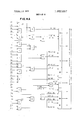
- FIG. 1 represents an encoding circuit arrangement which may contain the subject invention for recording digital signals on a magnetic storage medium.
- FIG. 2 shows a decoding circuit arrangement which may contain the subject invention for detecting information previously recorded on a magnetic storage me- 7 dia.
- the invention to record information on a magnetic storage medium.
- FIG. 6 illustrates examples of electrical switching patterns which may be generated by the invention.
- FIG. 1 illustrates a general encoding scheme for serially writing signals on a magnetic storage medium.
- the data to be written is received in groups of bits, such as the conventional byte format of eight information bits from a data processing system, e.g. central processing unit, channel, or control unit.
- An encoder-and serializer generate a modulated electrical waveform from each received groups of bits.
- the modulated waveform is transmitted to write circuits, and then to a write head, which transmits the waveform for recording onto a storage medium, e.g. magnetic disk surface.
- FIGS. 3A, 3B and.3C Detailed circuits for electrically performing the en coding operation are shown in FIGS. 3A, 3B and.3C.
- the waveform generated by this invention embodiment with a switch 301 (FIG. 3C) in its illustrated position is formed by'permuted electrical switchings in a '13 clock period cycle, having run-length-limits from two to eight clock periods.
- FIG. 3A illustrates a byte'input register containing eight information bit positions B through B7 which receives a group of information bits wh'ich may be provided as byte having eight parallel bits.
- Each position in the input register has bothtrue (T) and complimentary (C) output lines, e.g. B0and E0, etc.
- the output .of the register in FIG. 3A is providedas aninput to the encoder circuits shown in FIGS. 3C.
- FIG. 38 illustrates a conventional type of clock circuit, driven by a-free-running oscillator.
- the l ock has l3 pairs of output lines T1, T1 through T13, T13 which define 13 separate clock periods that time the operation of the encoder circuit.
- Each clock position provides true and complementary outputs, e.g. T1 for true output and T l for its complementary output.
- the clock only has one of the output of II T13 in an up voltage state at any one time, and all of its other outputs are then in their down voltage state.
- a pulse is provided first from lead Tl, then from lead T2, etc. through output T13 and back to output T1, etc. in a continuously cyclic manner comprising a cycle of 13 sequential clock pulsesd'efinirig the 13 clock periods.
- the clock circuit may be a shift register with endaround feedback having 13 latch. positions with only one of the positionsin a set state which is continuously communication transmitter via terminal 100, or to write circuit 101 which shape, amplify and provide the signal current to a recording head that writes the signals as flux switching between two magnetic states on a moving magnetic surface, e.g. magnetic disk.
- the encoder in FIG. 3C also generates a clock continuity signal W to signal to the next group of bits whether or not a flux switching occurred during the last clock pulse T13in the recorded waveform for the immediately'prior group of bits.
- a latch 102 which is set by an output from serializer AND circuit 103 to provide the output signal W.
- Latch 102 is reset by clock pulse T2, since the W output of the latch is only used during clock pulse T1 by AND circuit 104 of the encoder. (However latch 102 could be reset by any of the clock pulses up to the penultimate pulse T12.)
- the connections among the AND circuits & and OR circuits 0 in FIG. 3C is completely illustrated.
- FIG. 5A, 5B and 5C show the electrical waveforms generated by the encoder and serializer in FIG. 3C.
- Specific modulation patterns for five bit groups (B0 B4) are illustrated in eight clock pulse periods (I1 T8) on the left side of FIG. 5A; and, specific modulation patterns for three bit groups are illustrated in five clock pulse periods (T9 T13) on the right side of FIG. 5A.
- Any specific eight bit group is formed by co'ncatenating a five bit group and a three bit group, and the specific modulation pattern is obtained by concatenating their corresponding modulation patterns (i.e. eight ,period pattern and five period pattern.)
- Specific byte niodulation waveform examples having eight bit groups are shown in FIG. 6.
- v 1 U The digital modulation patterns in-FIGS.5A and 6 comprise electrical switchings betweentwo DC current levels which can be transmitted and recorded as flux switchings between two magnetization levels on a magnetic surface.
- the modulation is done in two sections foreach eight bit group.
- the first section permutes the switchings during clock periods T2 through T8 in response to the being circulated as the shift register is driven by the'oscillator.
- each of 13 latches in the shift register is continuously providing both true and complementary outputs as inputs to the serializer in FIG. 3C.
- the circuit arrangement for the encoder in FIG. 3C receives each byte on the eight parallel information bit lines B0 through B7 provided from the byte input register in FIG. 3A.
- the encoder in FIG. 3C encodes the eight information bits in each received byte into 13 separate electrical states provided on the encoders 13 output lines to the serializer also shown in FIG. 3C.
- the serializer comprises 13 AND gates which respec- I -tively receive the 13 output lines from the encoder, and
- the allowable patterns in section] have at least one switching in T2 through T8.
- Section 2 permutes the switchings during clock periods T10 through T13 in reponse to the binary combination of the second group of information bits 5, 6, and 7 in the byte.
- the allowable patterns in FIG. 5A insections '1 and 2 can have no information modulation.switching in their boundary clock periods T1 and T9. N0 pattern has switchings in any two adjacent periods.
- the switching pattern at clock periodTl or 'l9 is a special case which does not depend directly upon the information bits but depends upon the proximity of modulation switchings i.e. switchings in clock periods adjacent to clock periods T1 and T9.
- the allowable switching patterns for clock period T1 are shown in FIG.'5B, which shows a switching at time T1 only if there is no switching at either time T2 or at time T0 (i.e. the prior T13).
- T9 as shown in FIG. 5C, a switching isallowable at T9 only if there is no switching at either of adjacent clock periods T8 or T10.
- the modulation waveform for the section 1 clock periods T1 through T8- is therefore catenated with the modulation waveform for the section two clock periods T9 through T13 to obtain.
- the 256 separately discernples of the types of modulations that can occur.
- the controlling clock period T i.e. prior T13
- FIG. 6 i.e. whether or not a switching occurred in the immediately preceding T13, which is'arbitrarily assumed not to have switched for the th, 6th, and 7th waveforms from the top of FIG. 6, but such T1 switching could not have occurred in these same waveforms if the prior cycle T0 had switched.
- T1 does not have a switching on the assumption that the prior clock period T0 had a switching; but if such prior period T0 did not have switching, the switching would then occur at T1.
- FIG. 2 illustrates a general detecting arrangement which can embody this invention.
- Digital signals are read by a magnetic head from a magnetic storage medium, e.g. magnetic disk surface.
- a read head senses the flux switchings on the magnetic surface as an electrical wave having pulses related to the timing of the flux switchings sensed from the magneticsurface.
- the sensed pulses are provided to a read circuit which may be a pulse peak detector of the type commercially used for detecting the time positions of flux reversal recordings on magnetic surfaces to generate narrow pulses which precisely relate their phasing to the flux switching positions on the magnetic surface.
- the read circuit pulses are provided to a decoder which decodes the pulses into information bits which are provided to a parallelizer which accummulates the bits of each byte for parallel transmission to a control unit, channel, or central processing unit.
- FIG. 4 shows a detailed drawing of a demodulator embodiment of this invention within the decoding scheme shown in FIG. 2 in which a magnetic head senses the flux recorded on the moving magnetic disk surface to generate therefrom anelectrical signal which is transmitted to a read circuit which precisely detects the flux switchings.
- the pulses at the output of the read circuit represent the modulated waves provided by the modulator which generated the signals, but in a different form than shown in FIG. 6. That is, a pulse is provided at each switching instead of the current reversal, so that. the modulation is effectively represented like it was originally generated.
- a phaselocked oscillator of conventional type ceives the pulse-timed output from the read circuit and synchronizes its'output pulses in precise phase with the flux-switchings on the magnetic surface.
- Phase locked oscillators are well known in the art and commercially used, for example, in digital magnetic tape drives such as the IBM 2420, etc.
- a clock receives the output of the phase lock oscillator in FIG. 4 and generates a sequence of clock period pulses on its respective output lines Tl through T13.
- the clock in FIG. 4 may be identical to, or may be the same, clock circuit shown in FIG. 3B used in the modulation embodiment.
- the output of the read circuit is provided to a demodulator circuit comprising pulse segregator circuits, decoder circuits, and a parallelizer.
- the read circuit output is received by each of 13 AND circuits that also respectively received the clock period lines TI through T13 to segregate the flux switching pulses on 13 separate lines Pl P13 in accordance with the time position of the read circuit pulses on a scale of 13 determined by the respective clock period signals on lines T1 T13.
- the segregated signals on lines P1 through P13 are provided as inputs to the decoder circuits, which are shown in detail in FIG. 4A.
- the eight outputs from the decoder circuits are provided to a parallelizer which is a register that collects the decodedinformation bits B0 B7 as they occurred when originally provided to the modulator input register in FIG. 3A.
- the demodulated byte output from the parallelizer is available at its output between clock period signal T13 and the next clock period signal T1, during which the output byte is accepted by the system.
- FIG. 4A illustrates the decoder circuits in detail and shows precisely its connections to segregator leads P1 through P13.
- the pulses from clock period leads'Tl and T9 control reset functions in the decoder circuits. (Note that the clock always provides a pulse at clock periods T1 and T9, even though no pulse switching is provided at these times in the modulated signal from the read circuit).
- the detailed encodercircuit drawing shown in detail in FIG. 4A is self explanatory, and it comprises AND circuits A, OR circuits 0 and latch L circuits, each of which is a well known type ,of circuit.
- the p'arallelizer comprises register positions B0 through B7 in the conventional circuit form. Each register position has set and reset inputs and is reset at clock period T1, except that position B4 is also reset by a pulse on lead P8 so that it can obtain the correct output. I
- the described embodiment uses the correspondence between the information bits and the switching patterns shown in FIG. 5A.
- the order of the information bit patterns in FIG. 5A may change to have any one-to-one relationship to the illustrated order of switching patterns.
- the encoding and decoding circuits can be readily changed to correspond to any such coding relationship selected.
- Groups of five serial information bits can also be encoded using the circuit shown in FIG. 3C by-reversing the illustrated setting of a switch 301.
- the decoder in FIG. 4A will automatically handle the received five bit encoded switching sections, i.e. in eight clock periods. In this case the is, the boundaries for the five information bit groups need not align with the byte boundaries.
- 8 to 5 and 5 to 8 bit byte converters are used respectively before encoding and after decoding to interface the embodiment described herein for encoding and decoding the five bit groups in eight clock period cycles.
- the right side of FIG. A illustrates five bit codes and corresponding eight bit period switching patterns, ie from T1 through T8.
- an encoder circuit having first and second parts respectively receiving the first and second groups of electrical bit signals and the timing pulses of the first and second sequential clock pulse sections
- the first part in said encoder circuit having means for switching a firstele ctrical waveform between two electrical levels with the first group of electrical bit signals and the timing pulses of the first sequential clock pulse section to generate a different electrical waveform for each different combination of electrical bit signals in said first group, the electrical switchings in the first waveform being spaced by at least two clock periods during said first sequential clock pulse section, a nd said first waveform excluding a bounding clock period of the first section,
- the second part in said encoder circuit having means for switching a second electrical waveform between two electrical levels with the second group of electrical bit signals and the timing pulses of the second sequential clock pulse section to generate a different electrical waveform for each combination of electrical bit signals in the second group, the
- Electrical apparatus for modulating an electrical output with electrical bit signals for each received information group comprising *a clock circuit for generating a set of electrical timing pulses for each received information group'to sequentially provide a plurality of clock periods in a sequential clock pulse section,
- an encoder circuit receiving the electrical bit signals of said information group and the timing pulses from the sequential clock pulse section
- said encoder circuit including means for switching an electrical waveform between two electrical levels with the electrical bit signals and the timing pulses-from the sequential clock -pulse section to generate a different waveform for each different combination of electrical bit signals in said received information groups, in which each waveform has switchings spaced by atleasttwo clock periods,
- Another part of said encoder circuit including means for bounding the electrical waveform on one side with a bounding clock period not used to encode any bits of the received information group,
- said encoder circuit further switching the electrical waveform during each bounding clock periodif no waveform switching occurs in adjacent clock periods
- An electrical byte modulating method which handles the bits of each received byte provided as first and second groups of electrical bit signals, comprising the steps of generating in a clock circuit a set of electrical timing pulses for each received byte to sequentially provide a plurality of clock periods from first and second sequential clock pulse sections,
- said bounding step applies to the first clock period in each clock section
- An electrical byte modulating method which handles the bits of each received information group, com- 5 prising the steps of generating in a clock circuit a set of electrical timing pulses for each received information group to sequentially provide a plurality of clock periods in a sequential clock pulse section,
Landscapes
- Engineering & Computer Science (AREA)
- Signal Processing (AREA)
- Physics & Mathematics (AREA)
- Spectroscopy & Molecular Physics (AREA)
- Computer Networks & Wireless Communication (AREA)
- Dc Digital Transmission (AREA)
- Signal Processing For Digital Recording And Reproducing (AREA)
- Compression, Expansion, Code Conversion, And Decoders (AREA)
Priority Applications (7)
| Application Number | Priority Date | Filing Date | Title |
|---|---|---|---|
| US00375405A US3852687A (en) | 1973-07-02 | 1973-07-02 | High rate digital modulation/demodulation method |
| IT22723/74A IT1012368B (it) | 1973-07-02 | 1974-05-15 | Circuito e sistema di modulazione demodulazione |
| FR7417753A FR2236312B1 (cg-RX-API-DMAC7.html) | 1973-07-02 | 1974-05-15 | |
| JP6880174A JPS5421046B2 (cg-RX-API-DMAC7.html) | 1973-07-02 | 1974-06-18 | |
| GB2714874A GB1462889A (en) | 1973-07-02 | 1974-06-19 | Electrical encoding and decoding apparatus |
| CA203,323A CA1021464A (en) | 1973-07-02 | 1974-06-25 | High rate digital modulation/demodulation method and means |
| DE2430685A DE2430685A1 (de) | 1973-07-02 | 1974-06-26 | Verfahren und vorrichtung zur schnellen digitalen modulation |
Applications Claiming Priority (1)
| Application Number | Priority Date | Filing Date | Title |
|---|---|---|---|
| US00375405A US3852687A (en) | 1973-07-02 | 1973-07-02 | High rate digital modulation/demodulation method |
Publications (1)
| Publication Number | Publication Date |
|---|---|
| US3852687A true US3852687A (en) | 1974-12-03 |
Family
ID=23480772
Family Applications (1)
| Application Number | Title | Priority Date | Filing Date |
|---|---|---|---|
| US00375405A Expired - Lifetime US3852687A (en) | 1973-07-02 | 1973-07-02 | High rate digital modulation/demodulation method |
Country Status (7)
| Country | Link |
|---|---|
| US (1) | US3852687A (cg-RX-API-DMAC7.html) |
| JP (1) | JPS5421046B2 (cg-RX-API-DMAC7.html) |
| CA (1) | CA1021464A (cg-RX-API-DMAC7.html) |
| DE (1) | DE2430685A1 (cg-RX-API-DMAC7.html) |
| FR (1) | FR2236312B1 (cg-RX-API-DMAC7.html) |
| GB (1) | GB1462889A (cg-RX-API-DMAC7.html) |
| IT (1) | IT1012368B (cg-RX-API-DMAC7.html) |
Cited By (12)
| Publication number | Priority date | Publication date | Assignee | Title |
|---|---|---|---|---|
| US4398225A (en) * | 1981-04-24 | 1983-08-09 | Iomega Corporation | Combined serializer encoder and decoder for data storage system |
| US4496934A (en) * | 1980-09-05 | 1985-01-29 | Mitsubishi Denki Kabushiki Kaisha | Encoding and decoding systems for binary data |
| US4536742A (en) * | 1982-09-15 | 1985-08-20 | U.S. Philips Corporation | Method of encoding a stream of data bits, device for carring out the method, and device for decoding a stream of data bits |
| US4689757A (en) * | 1983-01-17 | 1987-08-25 | Vada Systems, Inc. | Machine event processing system |
| EP0147090A3 (en) * | 1983-12-29 | 1987-10-07 | Laser Magnetic Storage International Company | High density code for coded optical recording of binary data |
| US4802154A (en) * | 1983-10-13 | 1989-01-31 | Laser Magnetic Storage International Company | High density codes for optical recording |
| EP0205009A3 (en) * | 1985-06-13 | 1989-05-03 | International Business Machines Corporation | System for encoding a data stream into a run length limited symbol string |
| US4833470A (en) * | 1986-07-15 | 1989-05-23 | Matsushita Electric Industrial Co., Ltd. | Code conversion apparatus |
| US5392168A (en) * | 1990-08-31 | 1995-02-21 | Matsushita Electric Industrial Co., Ltd. | Method of recording digital video and audio data |
| EP0652562A1 (en) * | 1993-11-10 | 1995-05-10 | STMicroelectronics S.r.l. | Programmable single/dual output data streams RLL/NRZ decoder |
| US5528237A (en) * | 1993-09-21 | 1996-06-18 | Sgs-Thomson Microelectronics, Srl | Pipelined decoder for high frequency operation |
| US6687066B1 (en) * | 1999-02-22 | 2004-02-03 | Seagate Technology Llc | Partitioning disc drive read/write electronics to improve data transfer performance |
Families Citing this family (2)
| Publication number | Priority date | Publication date | Assignee | Title |
|---|---|---|---|---|
| US4544962A (en) * | 1981-07-06 | 1985-10-01 | Matsushita Electric Industrial Co., Ltd. | Method and apparatus for processing binary data |
| GB2141906A (en) * | 1983-06-20 | 1985-01-03 | Indep Broadcasting Authority | Recording of digital information |
Citations (1)
| Publication number | Priority date | Publication date | Assignee | Title |
|---|---|---|---|---|
| US3587090A (en) * | 1967-05-24 | 1971-06-22 | Jean A Labeyrie | Great rapidity data transmission system |
Family Cites Families (3)
| Publication number | Priority date | Publication date | Assignee | Title |
|---|---|---|---|---|
| US3215779A (en) * | 1961-02-24 | 1965-11-02 | Hallicrafters Co | Digital data conversion and transmission system |
| DE1211687B (de) * | 1964-11-10 | 1966-03-03 | Telefunken Patent | System zur linearen systematischen Kodierung |
| US3689899A (en) * | 1971-06-07 | 1972-09-05 | Ibm | Run-length-limited variable-length coding with error propagation limitation |
-
1973
- 1973-07-02 US US00375405A patent/US3852687A/en not_active Expired - Lifetime
-
1974
- 1974-05-15 IT IT22723/74A patent/IT1012368B/it active
- 1974-05-15 FR FR7417753A patent/FR2236312B1/fr not_active Expired
- 1974-06-18 JP JP6880174A patent/JPS5421046B2/ja not_active Expired
- 1974-06-19 GB GB2714874A patent/GB1462889A/en not_active Expired
- 1974-06-25 CA CA203,323A patent/CA1021464A/en not_active Expired
- 1974-06-26 DE DE2430685A patent/DE2430685A1/de active Pending
Patent Citations (1)
| Publication number | Priority date | Publication date | Assignee | Title |
|---|---|---|---|---|
| US3587090A (en) * | 1967-05-24 | 1971-06-22 | Jean A Labeyrie | Great rapidity data transmission system |
Cited By (13)
| Publication number | Priority date | Publication date | Assignee | Title |
|---|---|---|---|---|
| US4496934A (en) * | 1980-09-05 | 1985-01-29 | Mitsubishi Denki Kabushiki Kaisha | Encoding and decoding systems for binary data |
| US4398225A (en) * | 1981-04-24 | 1983-08-09 | Iomega Corporation | Combined serializer encoder and decoder for data storage system |
| US4536742A (en) * | 1982-09-15 | 1985-08-20 | U.S. Philips Corporation | Method of encoding a stream of data bits, device for carring out the method, and device for decoding a stream of data bits |
| US4689757A (en) * | 1983-01-17 | 1987-08-25 | Vada Systems, Inc. | Machine event processing system |
| US4802154A (en) * | 1983-10-13 | 1989-01-31 | Laser Magnetic Storage International Company | High density codes for optical recording |
| EP0147090A3 (en) * | 1983-12-29 | 1987-10-07 | Laser Magnetic Storage International Company | High density code for coded optical recording of binary data |
| EP0205009A3 (en) * | 1985-06-13 | 1989-05-03 | International Business Machines Corporation | System for encoding a data stream into a run length limited symbol string |
| US4833470A (en) * | 1986-07-15 | 1989-05-23 | Matsushita Electric Industrial Co., Ltd. | Code conversion apparatus |
| US5392168A (en) * | 1990-08-31 | 1995-02-21 | Matsushita Electric Industrial Co., Ltd. | Method of recording digital video and audio data |
| US5528237A (en) * | 1993-09-21 | 1996-06-18 | Sgs-Thomson Microelectronics, Srl | Pipelined decoder for high frequency operation |
| US5521598A (en) * | 1993-10-11 | 1996-05-28 | Sgs-Thomson Microelectronics, Srl | RLL/NRZ decoder programmable for single/dual bit output data streams |
| EP0652562A1 (en) * | 1993-11-10 | 1995-05-10 | STMicroelectronics S.r.l. | Programmable single/dual output data streams RLL/NRZ decoder |
| US6687066B1 (en) * | 1999-02-22 | 2004-02-03 | Seagate Technology Llc | Partitioning disc drive read/write electronics to improve data transfer performance |
Also Published As
| Publication number | Publication date |
|---|---|
| JPS5421046B2 (cg-RX-API-DMAC7.html) | 1979-07-27 |
| CA1021464A (en) | 1977-11-22 |
| FR2236312A1 (cg-RX-API-DMAC7.html) | 1975-01-31 |
| GB1462889A (en) | 1977-01-26 |
| FR2236312B1 (cg-RX-API-DMAC7.html) | 1976-06-25 |
| IT1012368B (it) | 1977-03-10 |
| DE2430685A1 (de) | 1975-01-30 |
| JPS5039117A (cg-RX-API-DMAC7.html) | 1975-04-11 |
Similar Documents
| Publication | Publication Date | Title |
|---|---|---|
| US5537112A (en) | Method and apparatus for implementing run length limited codes in partial response channels | |
| US3852687A (en) | High rate digital modulation/demodulation method | |
| JPH0158705B2 (cg-RX-API-DMAC7.html) | ||
| US4598267A (en) | Method and apparatus for converting a digital signal | |
| JPH0544206B2 (cg-RX-API-DMAC7.html) | ||
| US4310860A (en) | Method and apparatus for recording data on and reading data from magnetic storages | |
| US4456905A (en) | Method and apparatus for encoding binary data | |
| US5535187A (en) | High capacity run-length-limited coding system employing asymmetric and even-spaced codes | |
| JPS62250748A (ja) | 符号変換装置 | |
| US3685033A (en) | Block encoding for magnetic recording systems | |
| US3564557A (en) | Self-clocking recording | |
| JPS6226102B2 (cg-RX-API-DMAC7.html) | ||
| JP3935217B2 (ja) | mビット情報ワードのシーケンスから変調信号への変換 | |
| US3827078A (en) | Digital data retrieval system with dynamic window skew | |
| US4482927A (en) | Ternary magnetic recording and reproducing system with simultaneous overwrite | |
| US3631463A (en) | Self-clocked encoding scheme | |
| EP0090047B1 (en) | Encoding and decoding system for binary data | |
| US4868922A (en) | Data modulation/demodulation system utilizing demodulation clocks that differ in phase | |
| JPS6313425A (ja) | 情報デ−タ復元装置 | |
| KR960006396B1 (ko) | 디지틀신호 기록방법 | |
| US4544961A (en) | Triplex digital magnetic recording and reproducing system | |
| JPH0462216B2 (cg-RX-API-DMAC7.html) | ||
| US3493962A (en) | Converter for self-clocking digital signals | |
| JPS634269B2 (cg-RX-API-DMAC7.html) | ||
| JPH05509448A (ja) | 2進信号のバンド幅の制限方法および装置 |