US3700960A - Metal halide lamp system - Google Patents
Metal halide lamp system Download PDFInfo
- Publication number
- US3700960A US3700960A US183094A US3700960DA US3700960A US 3700960 A US3700960 A US 3700960A US 183094 A US183094 A US 183094A US 3700960D A US3700960D A US 3700960DA US 3700960 A US3700960 A US 3700960A
- Authority
- US
- United States
- Prior art keywords
- lamp
- source
- circuit
- control means
- current
- Prior art date
- Legal status (The legal status is an assumption and is not a legal conclusion. Google has not performed a legal analysis and makes no representation as to the accuracy of the status listed.)
- Expired - Lifetime
Links
- 229910001507 metal halide Inorganic materials 0.000 title abstract description 17
- 150000005309 metal halides Chemical class 0.000 title abstract description 17
- 230000003595 spectral effect Effects 0.000 claims abstract description 24
- 230000000694 effects Effects 0.000 claims abstract description 11
- 239000004065 semiconductor Substances 0.000 claims abstract description 11
- 229910052751 metal Inorganic materials 0.000 claims abstract description 8
- 239000002184 metal Substances 0.000 claims abstract description 8
- 230000005855 radiation Effects 0.000 claims description 12
- 239000000969 carrier Substances 0.000 claims description 4
- 125000004122 cyclic group Chemical group 0.000 claims 1
- 238000001962 electrophoresis Methods 0.000 abstract description 6
- 150000002739 metals Chemical class 0.000 abstract description 3
- 238000009826 distribution Methods 0.000 description 7
- VYPSYNLAJGMNEJ-UHFFFAOYSA-N silicon dioxide Inorganic materials O=[Si]=O VYPSYNLAJGMNEJ-UHFFFAOYSA-N 0.000 description 5
- 238000003860 storage Methods 0.000 description 5
- 230000007704 transition Effects 0.000 description 5
- XKRFYHLGVUSROY-UHFFFAOYSA-N Argon Chemical compound [Ar] XKRFYHLGVUSROY-UHFFFAOYSA-N 0.000 description 4
- 238000010586 diagram Methods 0.000 description 4
- HSZCZNFXUDYRKD-UHFFFAOYSA-M lithium iodide Chemical compound [Li+].[I-] HSZCZNFXUDYRKD-UHFFFAOYSA-M 0.000 description 4
- QSHDDOUJBYECFT-UHFFFAOYSA-N mercury Chemical compound [Hg] QSHDDOUJBYECFT-UHFFFAOYSA-N 0.000 description 4
- 229910052753 mercury Inorganic materials 0.000 description 4
- 230000001276 controlling effect Effects 0.000 description 3
- 239000010453 quartz Substances 0.000 description 3
- 229910052720 vanadium Inorganic materials 0.000 description 3
- 229910052786 argon Inorganic materials 0.000 description 2
- 238000006243 chemical reaction Methods 0.000 description 2
- 238000000576 coating method Methods 0.000 description 2
- 230000006872 improvement Effects 0.000 description 2
- 238000006116 polymerization reaction Methods 0.000 description 2
- 230000004044 response Effects 0.000 description 2
- CMJCEVKJYRZMIA-UHFFFAOYSA-M thallium(i) iodide Chemical compound [Tl]I CMJCEVKJYRZMIA-UHFFFAOYSA-M 0.000 description 2
- WFKWXMTUELFFGS-UHFFFAOYSA-N tungsten Chemical compound [W] WFKWXMTUELFFGS-UHFFFAOYSA-N 0.000 description 2
- UAYWVJHJZHQCIE-UHFFFAOYSA-L zinc iodide Chemical compound I[Zn]I UAYWVJHJZHQCIE-UHFFFAOYSA-L 0.000 description 2
- WHXSMMKQMYFTQS-UHFFFAOYSA-N Lithium Chemical compound [Li] WHXSMMKQMYFTQS-UHFFFAOYSA-N 0.000 description 1
- ZOKXTWBITQBERF-UHFFFAOYSA-N Molybdenum Chemical compound [Mo] ZOKXTWBITQBERF-UHFFFAOYSA-N 0.000 description 1
- HCHKCACWOHOZIP-UHFFFAOYSA-N Zinc Chemical compound [Zn] HCHKCACWOHOZIP-UHFFFAOYSA-N 0.000 description 1
- 230000008901 benefit Effects 0.000 description 1
- 239000003990 capacitor Substances 0.000 description 1
- 239000011248 coating agent Substances 0.000 description 1
- 239000003086 colorant Substances 0.000 description 1
- 230000001934 delay Effects 0.000 description 1
- 125000000664 diazo group Chemical group [N-]=[N+]=[*] 0.000 description 1
- 238000001035 drying Methods 0.000 description 1
- 239000000835 fiber Substances 0.000 description 1
- 230000004907 flux Effects 0.000 description 1
- 239000011888 foil Substances 0.000 description 1
- 239000005350 fused silica glass Substances 0.000 description 1
- 238000009413 insulation Methods 0.000 description 1
- 229910052744 lithium Inorganic materials 0.000 description 1
- 238000004519 manufacturing process Methods 0.000 description 1
- 239000000463 material Substances 0.000 description 1
- 238000005259 measurement Methods 0.000 description 1
- 229910001511 metal iodide Inorganic materials 0.000 description 1
- 238000000034 method Methods 0.000 description 1
- 229910052750 molybdenum Inorganic materials 0.000 description 1
- 239000011733 molybdenum Substances 0.000 description 1
- 230000010355 oscillation Effects 0.000 description 1
- 239000003973 paint Substances 0.000 description 1
- 229920002120 photoresistant polymer Polymers 0.000 description 1
- 230000008569 process Effects 0.000 description 1
- 238000005086 pumping Methods 0.000 description 1
- 230000001172 regenerating effect Effects 0.000 description 1
- 230000001105 regulatory effect Effects 0.000 description 1
- 230000035945 sensitivity Effects 0.000 description 1
- 238000001228 spectrum Methods 0.000 description 1
- 229910052716 thallium Inorganic materials 0.000 description 1
- -1 thallium iodides Chemical class 0.000 description 1
- ZCUFMDLYAMJYST-UHFFFAOYSA-N thorium dioxide Chemical compound O=[Th]=O ZCUFMDLYAMJYST-UHFFFAOYSA-N 0.000 description 1
- 229910003452 thorium oxide Inorganic materials 0.000 description 1
- RMUKCGUDVKEQPL-UHFFFAOYSA-K triiodoindigane Chemical compound I[In](I)I RMUKCGUDVKEQPL-UHFFFAOYSA-K 0.000 description 1
- 229910052725 zinc Inorganic materials 0.000 description 1
- 239000011701 zinc Substances 0.000 description 1
Images


Classifications
-
- H—ELECTRICITY
- H05—ELECTRIC TECHNIQUES NOT OTHERWISE PROVIDED FOR
- H05B—ELECTRIC HEATING; ELECTRIC LIGHT SOURCES NOT OTHERWISE PROVIDED FOR; CIRCUIT ARRANGEMENTS FOR ELECTRIC LIGHT SOURCES, IN GENERAL
- H05B41/00—Circuit arrangements or apparatus for igniting or operating discharge lamps
- H05B41/14—Circuit arrangements
- H05B41/36—Controlling
- H05B41/38—Controlling the intensity of light
- H05B41/39—Controlling the intensity of light continuously
- H05B41/392—Controlling the intensity of light continuously using semiconductor devices, e.g. thyristor
- H05B41/3921—Controlling the intensity of light continuously using semiconductor devices, e.g. thyristor with possibility of light intensity variations
- H05B41/3922—Controlling the intensity of light continuously using semiconductor devices, e.g. thyristor with possibility of light intensity variations and measurement of the incident light
-
- G—PHYSICS
- G03—PHOTOGRAPHY; CINEMATOGRAPHY; ANALOGOUS TECHNIQUES USING WAVES OTHER THAN OPTICAL WAVES; ELECTROGRAPHY; HOLOGRAPHY
- G03B—APPARATUS OR ARRANGEMENTS FOR TAKING PHOTOGRAPHS OR FOR PROJECTING OR VIEWING THEM; APPARATUS OR ARRANGEMENTS EMPLOYING ANALOGOUS TECHNIQUES USING WAVES OTHER THAN OPTICAL WAVES; ACCESSORIES THEREFOR
- G03B27/00—Photographic printing apparatus
- G03B27/72—Controlling or varying light intensity, spectral composition, or exposure time in photographic printing apparatus
- G03B27/73—Controlling exposure by variation of spectral composition, e.g. multicolor printers
Definitions
- ..315/l5l 250/205, 250/226, and the factors primarily responsible for it are 313/229, 315/155, 315/158, 323/21 cataphoresis and thermal gradients.
- the cataphoretic [51] Int. Cl. ..H05b 37/02 effect is the stronger and the nonuniformity may b 58 Field of Search ..315/l5l, 158, 155; 250/205, Overcome y pp y a DC component to the 25002 323 21; 313 discharge current and controlling its polarity and magnitude.
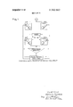
- the lamp is operated from a DC [56] References Cited power supply through a control circuit using semi-conductors for polarity reversing switches wherein the UNITED STATES PATENTS time of current flow in one polarity is determined by 2,749,501 6/1956 Bartlett ..315/158 g i i and degree unbalance the spectral 3,431,427 3/1969 Pahl, Jr ..3l5/151 10 Claims, 5 Drawing Figures LUS & pus r- 9*- *EEF LLS p p ELS OPERA TIONHL flMPL/F/EE POWER CON T201.
- Examples of industrial applications are diazo printing requiring peak output in the 3500 to 4000 A regiomphoto polymerization reactions primarily sensitive in the 2000 to 2500 A region, polymerization of photo resists in the region below 2000 A,'paint drying and air curing of coatings in the range of 2500 to 4000 A.
- Radiation efiiciencies of metal halide lamps specifically designed to emit in selected wavelength regions may be several times higher in those regions than other types of discharges.
- metal halide discharges in T3 tubular inch arc tubes longer than 4 inches show in general at least 10 percent variation in spectral output from end to end and often as much as 100 percent when operated on alternating current.
- T3 tubular inch arc tubes longer than 4 inches show in general at least 10 percent variation in spectral output from end to end and often as much as 100 percent when operated on alternating current.
- the same lamps are operated on direct current, even greater nonuniformity results with vapor species being pumped to one end or the other of the tube by electrophoresis.
- the direction and degree of pumping varies with the particular metal halide species and with the other metals present in the arc tube.
- thermal gradients may be caused by a non-uniform bulb temperature distribution, or be variations in bulb diameter, or by unbalanced electrode losses. Regenerative conditions may exist causing small unbalances to lead to large nonuniforrnities.
- Cataphoresis may result directly from the nature of the current used, for instance where the current is DC or where the current is AC which includes a DC component. Cataphoresis may also result from an unbalance in the electrode energy input which effectively creates a DC component.
- DC component may be supplied and controlled.
- One way which may be referred to as Variable Time Ratio Square Wave Operation, operates the lamp from a DC power supply through polarity reversing switches in the form of semiconductors.
- a control circuit is provided whereby the time of current flow in any one polarity is determined by the direction and degree of unbalance in the spectral output.
- the lamp In another circuit which may be referred to Audio Frequency with DC Offset Current, the lamp is operated directly from a high audio frequency power supply.
- An auxiliary control provides a parallel DC offset current to regulate the electro-phoretic effect in the lamp.
- FIG. 1 illustrates a long linear tubular metal halide lamp suitable for the invention.
- FIG. 2 compares the output distribution of the lamp of FIG. 1 under normal 60 hertz operation with that under controlled DC bias for three color bands.
- FIG. 3 is a functional block diagram of a DC bias control circuit for operating the lamp according to the invention.
- FIG. 4 shows waveform output of an operational amplifier in the control circuit.
- FIG. 5 is a detailed schematic diagram of the DC bias control circuit.
- FIG. 1 A slender tubular lamp suitable for operation according to the invention is illustrated in FIG. 1 comprising an arc tube 1 of quartz or fused silica.
- the tube may be of the size commonly referred to as T3 (tubular, it: inch dia.) having an inside diameter of about 8 millimeters and having sealed therein at opposite ends a pair of arcing electrodes 2,2 defining an arc gap of about 14 inches.
- T3 tubular, it: inch dia.
- the electrode inleads 3 have intermediate thin molybdenum foil sections 4 hermetically sealed through full diameter pinch seals 5 at the ends of the tube.
- the electrodes each comprise a double layer tungsten wire helix 6 wrapped around a tungsten core wire 7, and may be conventionally activated by thoriumoxide applied as a coating on the turns of the helix or filling the space or interstices between turns.
- quartz sleeves 8 extendingforward up to the electrode tips may be fitted over the ends of the lamp as illustrated.
- the space between the tube wall and the sleeve is filled with a refractory white insulation 9 of quartz fibers.
- FIG. 2 shows the output distribution for normal 60 hertz operation (dashed lines), and for operation with a controlled DC bias (solid lines) according to the invention, for the three color bands green, red and blue.
- the intensity is plotted as ordinate against the place of measurement along the length of the lamp as abscissa, and the improvement in uniformity is apparent.
- Operation with DC bias control permits the use of a greater variety of metal halides with more flexibility in the choice of spectral output. It reduces the need for close control of arc chamber parameters, thereby lowering the cost of manufacture and the shrinkage rate. It permits the use of very small chamberdiameters in linear lamps, for example in applications requiring critical focusing.
- FIG. 3 illustrates one scheme for controlling a DC bias current to regulate the spectral distribution of a metal halide discharge lamp.
- pair of photo sensors P1 and P2 responsive to light intensity are aimed at opposite ends of the lamp. Their signals are fed to a differential operational amplifier connected as a zero crossing detector. The output voltage of the operational amplifier is supplied to power control amplifiers which provide an on signal to the right or left upper transistor power switches (LUS or RUS), and to the diagonally opposite lower transistor power switch (RLS or LLS). The four transistor power switches determine the direction in which the DC supply current is allowed to flow through the lamp load.
- Photosensors P1 and P2 comprise photo transistors Q1 and Q2 aimed or optically coupled to receive radiation f ,f,, from opposite ends of the lamp 1. They determine the input voltage to the darlington photo amplifiers, 03,4 and Q5 ,0. To compensate for variation between the response of individual photo transistors to light flux, a sensitivity adjustment of the gain and output voltage level of the photo amplifiers is made by means of variable resistors R1 and R2 (of 50 kilohms) and R3 and R4 of 5 kilohms. The sensitivityadjustment also determines the overall response of the system to an imbalance of light at the lamp ends. It is adjusted to provide sufficiently fine control to meet the need for uniformity but not so high as to cause hunting or oscillation of the end to end light difference.
- the output of the photo amplifiers is combined with an alternating sine wave voltage from source AC and applied to the input terminals x and y of a conventional operational amplifier 0A connected as 'a zero crossing detector. If the input at terminal at exceeds that at terminal y, the output is negative;.if the input at terminal y exceeds that at terminal 1:, the output is positive.
- the control function is developed as follows.
- the input signal to the operational amplifier is the difference in voltage applied to terminals x and y and is given by:
- V, V,, Vsin wt+(V V where V sin wt is the alternating sine wave voltage from source AC, V, is the signal at x-due to sensor P1, and V is the signal at y'due to sensor P2.
- V V the input voltage to 0A is as shown in FIG. 4a.
- the output is negative, as shown in FIG. 4b and vice versa.
- V V then OA simply performs a squaring function on the input sine wave, as shown in FIG. 40.
- V V the input voltage is as shown in FIG. 4d, and the output voltage as shown in FIG. 4e.
- V is the peak of the sine wave
- At is the positive wave duration
- At is the negative wave duration. Its value can vary continuously from +V to V,, depending on the difference in the light output between the lamp ends.
- the control voltage must operate to balance the light output from opposite ends of the lamp.
- a dc voltage applied to the lamp will cause the light to increase at the cathode or negative end.
- the control circuitry must provide current through the lamp in a direction to counteract the sensed imbalance 'by reversing the dccomponent of current.
- a bridge circuit controls current flow from a constant current dc source 11.
- the bridge comprises four transistor power switches LUS, RUS, LLS and RLS, being left and right, upper and lower switches.
- the polarity of power application is determined by having LUS and RLS on at the same time as RUS and LLS are off, and vice versa.
- LUS andRLS, nor LLS and RLS should ever be on simultaneously, and it is desirable that the transition from one'polarity to, the other be made as rapidly as possible.
- Transistor 07 is a very high gain transistor and serves to increase the level of the output from operational amplifier CA as well as to speed up the voltage reversal rate to approximately 20,000 volt/sec.
- Transistor Q8 inverts the output of Q7, that is reverses its phase. Transistors 07 and Q8 thus provide the out of phase on and off control signals necessary to obtain the proper application of power to the lamp through the power switches.
- Transistors 09,10 and 011,12 provide high peak power capacity for driving the principal drive transistors 013,14 and 015,16 as rapidly as possible.
- the associated circuitry provides isolated control of the tum on and turn off signals to maximize the speed and at the same time maintaining a very low dissipation. This permits lower cost low power transistors to be used for the drive transistors.
- upper power switches LUS and RUS have individual low voltage bias supplies consisting of the full wave rectified output of transformers T and T and the bias control transistors 017 and 018.
- the lower power switches LLS and RLS operate from a single bias supply (not shown) with similar circuitry connected to terminals 12 and 13. These bias supplies insure that the power switches are in saturation at the maximum current level required for the lamp.
- the principal drive transistors are connected to the base circuit of the bias control transistors 017,18 and 019,20 and when on remove the base drive from the power switch circuits.
- a problem with such circuitry arises from the fact that transistors turn on much more rapidly than 0 and turn off from saturation can be even longer due to stored charge in the transistors (storage time). Since LUS and LLS must never be on simultaneously (similarly RUS and RLS), the turn on of these transistors must. be made slower than the turn off including storage time, the reverse of the inherent tendency. While delay networks can be used, they become complicated and result in high dissipation in the power switches when long time periods are involved.
- the darlington connection .results in much longer charge storage and slower turn OK because the conventional means of charge removal consisting in reverse biasing the emitter-base junction, cannot be used.
- this handicap is overcome by means of pulldown diodes.
- the diodes D1, D2-5; D6, D740; D11, D12-15; and D16, D17-20 provide paths for removal of stored charge from each of the transistors through the principal drive transistors and thus serve to minimize the storage time.
- the improvement in performance is remarkable: typical storage time without these diodes is 20 microseconds or more; with the pulldown diodes, it is on the order of 2.5 microseconds.
- the problem is minimized.
- the transition In square wave operation, the transition must be sufiiciently rapid to limit the reignition voltage to the capa' bility of the dc power source. Transition times of the order of 20-30 microseconds can result in reignition voltages of -200 volts and can cause difficulty in the design of the power source. Therefore it is desirable to make the transition time less than 20 microseconds,
- a circuit for overcoming nonuniformity of radiant output along the length of an elongated metal vapor discharge lamp of a kind subject to electrophoretic effects comprising:
- sensing means responsive to unbalance in spectral output between the ends of said lamp
- control means responsive to said sensing means and providing current through said lamp with a dc component proportioned to create an electrophoretic effect overcoming said unbalance.
- a lamp as in claim 1 wherein said control means providescyclic reversals of current through said lamp in addition to said dc component.
- sensing means comprises a pair of radiation sensors optically coupled to opposite ends of said lamp, said source provides a controlled dc current, and said means for connecting the lamp across said source comprises a bridge circuit including four semiconductor switches controlled by said control means in pairs to determine the direction of current flow through said lamps.
- a circuit for overcoming nonuniformity of radiant output along the length of an elongated metal vapor 8. lamp of a kind subject to electrophoretic effects, comprising:
- I a bridge circuit comprising four semiconductor switches, 7 said source being connected across one diagonal of said bridge,- 7 terminals for connecting said lamp across the other diagonal of said bridg a pair of radiation sensors optically coupled to opposite ends of said lamp and responsive to the unbalance in spectral output therefrom,
- control means cyclically turning on” and off opposite pairs of said switches in order to provide alternating current flowfrom said source through said lamp
- control means being responsive to the signals from said sensors by varying the time of current flow in any one polarity in accordance with the direction and degree of unbalance in the spectral 8.
- said control means comprises an ac source and an operational amplifier, said operational amplifier providing a square wave output reversing at the frequency of said ac source with a ratio of time duration in opposite polarities following I the degree of unbalance in the spectral output.
- each of the four switches comprises two transistors connected emitter to base with common collectors in the darlington mode, and diodes connecting the bases of said transistors to said control means in order to achieve fast removal of stored carriers at turn off.
- control means comprises an ac source and an operational amplifier, said operational amplifier providing a square wave output reversing at the frequency of said ac source with a ratio of time duration in opposite polarities following the degree of unbalance in the spectral output, and each of the four switches comprises two transistors connected emitter to base with common collectors in the darlington mode, and diodes connecting the bases of said transistors to said control means in order to achieve fast removal of stored carriers at turn off.
Landscapes
- Physics & Mathematics (AREA)
- Spectroscopy & Molecular Physics (AREA)
- General Physics & Mathematics (AREA)
- Circuit Arrangements For Discharge Lamps (AREA)
- Discharge Lamps And Accessories Thereof (AREA)
Applications Claiming Priority (1)
| Application Number | Priority Date | Filing Date | Title |
|---|---|---|---|
| US18309471A | 1971-09-23 | 1971-09-23 |
Publications (1)
| Publication Number | Publication Date |
|---|---|
| US3700960A true US3700960A (en) | 1972-10-24 |
Family
ID=22671417
Family Applications (1)
| Application Number | Title | Priority Date | Filing Date |
|---|---|---|---|
| US183094A Expired - Lifetime US3700960A (en) | 1971-09-23 | 1971-09-23 | Metal halide lamp system |
Country Status (6)
| Country | Link |
|---|---|
| US (1) | US3700960A (Direct) |
| JP (1) | JPS4841565A (Direct) |
| CA (1) | CA1031407A (Direct) |
| DE (1) | DE2246234A1 (Direct) |
| FR (1) | FR2153366A1 (Direct) |
| NL (1) | NL7212886A (Direct) |
Cited By (16)
| Publication number | Priority date | Publication date | Assignee | Title |
|---|---|---|---|---|
| US3892961A (en) * | 1973-03-21 | 1975-07-01 | Intermadox A G | Contactless potentiometer with automatically controlled light source |
| US3904922A (en) * | 1973-11-19 | 1975-09-09 | Xerox Corp | Lamp control and lamp switch circuit |
| US3909609A (en) * | 1973-10-29 | 1975-09-30 | Xerox Corp | Light source measuring apparatus |
| US3993899A (en) * | 1973-12-13 | 1976-11-23 | Gunson's Sortex Limited | Sorting machine with fiber optic focusing means |
| US4004188A (en) * | 1975-09-26 | 1977-01-18 | General Electric Company | Starting circuit for inverter operated gaseous discharge lamps |
| DE2636876A1 (de) * | 1975-08-21 | 1977-02-24 | Mitsubishi Electric Corp | Verfahren zur mischbeleuchtung |
| US4012663A (en) * | 1974-11-25 | 1977-03-15 | General Electric Company | Lighting control system |
| DE2707987A1 (de) * | 1976-02-27 | 1977-09-15 | Mitsubishi Electric Corp | Beleuchtungsverfahren zur bildung farbiger schatten |
| US4190795A (en) * | 1977-09-09 | 1980-02-26 | Coberly & Associates | Constant intensity light source |
| US4360756A (en) * | 1979-11-13 | 1982-11-23 | General Electric Company | Metal halide lamp containing ThI4 with added elemental cadmium or zinc |
| US4697709A (en) * | 1985-09-03 | 1987-10-06 | Delta Technology Corporation | Sorter for agricultural products |
| US4803406A (en) * | 1984-11-05 | 1989-02-07 | Hitachi, Ltd. | High-pressure discharge lamp operating circuit |
| US5333034A (en) * | 1992-01-31 | 1994-07-26 | Bremson Data Systems, Inc. | System for selectively controlling the spectral make-up of visible light from a source thereof |
| US5581161A (en) * | 1994-07-13 | 1996-12-03 | Gong; Mingfu | DC coupled electronic ballast with a larger DC and smaller AC signal |
| US20040066153A1 (en) * | 2002-10-07 | 2004-04-08 | Nemirow Arthur T. | Electronic ballast with DC output flyback converter |
| US20040178746A1 (en) * | 2003-03-11 | 2004-09-16 | Bruce Industries, Inc. | Low frequency output electronic ballast |
Families Citing this family (2)
| Publication number | Priority date | Publication date | Assignee | Title |
|---|---|---|---|---|
| ZA824856B (en) * | 1981-07-28 | 1983-05-25 | Lee Electric Lighting | Power supply for arc lamps |
| JP2902272B2 (ja) * | 1993-08-27 | 1999-06-07 | 株式会社三協精機製作所 | 磁気カードリーダ |
Citations (2)
| Publication number | Priority date | Publication date | Assignee | Title |
|---|---|---|---|---|
| US2749501A (en) * | 1950-10-06 | 1956-06-05 | California Packing Corp | Photoelectric voltage regulator |
| US3431427A (en) * | 1965-10-24 | 1969-03-04 | Henry D Pahl Jr | Solid state color balance controller for incandescent lamps |
-
1971
- 1971-09-23 US US183094A patent/US3700960A/en not_active Expired - Lifetime
-
1972
- 1972-08-15 CA CA149,424A patent/CA1031407A/en not_active Expired
- 1972-09-21 JP JP47094151A patent/JPS4841565A/ja active Pending
- 1972-09-21 DE DE2246234A patent/DE2246234A1/de active Pending
- 1972-09-21 FR FR7233436A patent/FR2153366A1/fr not_active Withdrawn
- 1972-09-22 NL NL7212886A patent/NL7212886A/xx unknown
Patent Citations (2)
| Publication number | Priority date | Publication date | Assignee | Title |
|---|---|---|---|---|
| US2749501A (en) * | 1950-10-06 | 1956-06-05 | California Packing Corp | Photoelectric voltage regulator |
| US3431427A (en) * | 1965-10-24 | 1969-03-04 | Henry D Pahl Jr | Solid state color balance controller for incandescent lamps |
Cited By (18)
| Publication number | Priority date | Publication date | Assignee | Title |
|---|---|---|---|---|
| US3892961A (en) * | 1973-03-21 | 1975-07-01 | Intermadox A G | Contactless potentiometer with automatically controlled light source |
| US3909609A (en) * | 1973-10-29 | 1975-09-30 | Xerox Corp | Light source measuring apparatus |
| US3904922A (en) * | 1973-11-19 | 1975-09-09 | Xerox Corp | Lamp control and lamp switch circuit |
| US3993899A (en) * | 1973-12-13 | 1976-11-23 | Gunson's Sortex Limited | Sorting machine with fiber optic focusing means |
| US4012663A (en) * | 1974-11-25 | 1977-03-15 | General Electric Company | Lighting control system |
| DE2636876A1 (de) * | 1975-08-21 | 1977-02-24 | Mitsubishi Electric Corp | Verfahren zur mischbeleuchtung |
| US4004188A (en) * | 1975-09-26 | 1977-01-18 | General Electric Company | Starting circuit for inverter operated gaseous discharge lamps |
| DE2707987A1 (de) * | 1976-02-27 | 1977-09-15 | Mitsubishi Electric Corp | Beleuchtungsverfahren zur bildung farbiger schatten |
| US4190795A (en) * | 1977-09-09 | 1980-02-26 | Coberly & Associates | Constant intensity light source |
| US4360756A (en) * | 1979-11-13 | 1982-11-23 | General Electric Company | Metal halide lamp containing ThI4 with added elemental cadmium or zinc |
| US4803406A (en) * | 1984-11-05 | 1989-02-07 | Hitachi, Ltd. | High-pressure discharge lamp operating circuit |
| US4697709A (en) * | 1985-09-03 | 1987-10-06 | Delta Technology Corporation | Sorter for agricultural products |
| US5333034A (en) * | 1992-01-31 | 1994-07-26 | Bremson Data Systems, Inc. | System for selectively controlling the spectral make-up of visible light from a source thereof |
| US5581161A (en) * | 1994-07-13 | 1996-12-03 | Gong; Mingfu | DC coupled electronic ballast with a larger DC and smaller AC signal |
| US20040066153A1 (en) * | 2002-10-07 | 2004-04-08 | Nemirow Arthur T. | Electronic ballast with DC output flyback converter |
| US6864642B2 (en) | 2002-10-07 | 2005-03-08 | Bruce Industries, Inc. | Electronic ballast with DC output flyback converter |
| US20040178746A1 (en) * | 2003-03-11 | 2004-09-16 | Bruce Industries, Inc. | Low frequency output electronic ballast |
| US6879113B2 (en) | 2003-03-11 | 2005-04-12 | Bruce Industries, Inc. | Low frequency output electronic ballast |
Also Published As
| Publication number | Publication date |
|---|---|
| NL7212886A (Direct) | 1973-03-27 |
| DE2246234A1 (de) | 1973-03-29 |
| CA1031407A (en) | 1978-05-16 |
| JPS4841565A (Direct) | 1973-06-18 |
| FR2153366A1 (Direct) | 1973-05-04 |
Similar Documents
| Publication | Publication Date | Title |
|---|---|---|
| US3700960A (en) | Metal halide lamp system | |
| US2624858A (en) | Gaseous discharge lamp | |
| US4352045A (en) | Energy conservation system using current control | |
| US5949192A (en) | Operating apparatus for discharge lamp | |
| US5363019A (en) | Variable color discharge device | |
| JPH0529085A (ja) | 希ガス放電灯装置 | |
| JPH04324294A (ja) | 光放射電子管点灯装置 | |
| US3514667A (en) | Gas-filled discharge tube impulse control and operating apparatus | |
| KR20050007393A (ko) | 가스 방전 램프의 구동 방법 및 디바이스 | |
| US3603841A (en) | Fluorescent lamp device with luminosity control | |
| CA1260998A (en) | Adaption circuit for operating a high-pressure discharge lamp | |
| US3591828A (en) | Discharge lamp device and its operating apparatus | |
| US3465202A (en) | Electroluminescent device for deriving a bright output image from a dark input image | |
| JPS61118956A (ja) | 小型低圧水銀放電管 | |
| JP3121306B2 (ja) | 調光機能付き冷陰極放電管用インバータ回路 | |
| US966205A (en) | Apparatus for transforming electrical energy. | |
| SU437254A1 (ru) | Устройство дл питани газоразр дных ламп с подогревными электродами | |
| JPS59141158A (ja) | 平板形放電灯装置 | |
| SU964597A1 (ru) | Управл емый высоковольтный преобразователь напр жени | |
| JPH0696879A (ja) | 陰極放電管駆動用電源装置 | |
| JP2600646Y2 (ja) | 放電灯の点灯装置 | |
| US682691A (en) | Method of operating electric lamps. | |
| JPH0410393A (ja) | 希ガス放電灯点灯装置 | |
| JP2800418B2 (ja) | 水銀ディスペンサーの活性化方法 | |
| US1188575A (en) | Single-phase gas or vapor electric device. |