US3700960A - Metal halide lamp system - Google Patents
Metal halide lamp system Download PDFInfo
- Publication number
- US3700960A US3700960A US183094A US3700960DA US3700960A US 3700960 A US3700960 A US 3700960A US 183094 A US183094 A US 183094A US 3700960D A US3700960D A US 3700960DA US 3700960 A US3700960 A US 3700960A
- Authority
- US
- United States
- Prior art keywords
- lamp
- source
- circuit
- control means
- current
- Prior art date
- Legal status (The legal status is an assumption and is not a legal conclusion. Google has not performed a legal analysis and makes no representation as to the accuracy of the status listed.)
- Expired - Lifetime
Links
Images


Classifications
-
- H—ELECTRICITY
- H05—ELECTRIC TECHNIQUES NOT OTHERWISE PROVIDED FOR
- H05B—ELECTRIC HEATING; ELECTRIC LIGHT SOURCES NOT OTHERWISE PROVIDED FOR; CIRCUIT ARRANGEMENTS FOR ELECTRIC LIGHT SOURCES, IN GENERAL
- H05B41/00—Circuit arrangements or apparatus for igniting or operating discharge lamps
- H05B41/14—Circuit arrangements
- H05B41/36—Controlling
- H05B41/38—Controlling the intensity of light
- H05B41/39—Controlling the intensity of light continuously
- H05B41/392—Controlling the intensity of light continuously using semiconductor devices, e.g. thyristor
- H05B41/3921—Controlling the intensity of light continuously using semiconductor devices, e.g. thyristor with possibility of light intensity variations
- H05B41/3922—Controlling the intensity of light continuously using semiconductor devices, e.g. thyristor with possibility of light intensity variations and measurement of the incident light
-
- G—PHYSICS
- G03—PHOTOGRAPHY; CINEMATOGRAPHY; ANALOGOUS TECHNIQUES USING WAVES OTHER THAN OPTICAL WAVES; ELECTROGRAPHY; HOLOGRAPHY
- G03B—APPARATUS OR ARRANGEMENTS FOR TAKING PHOTOGRAPHS OR FOR PROJECTING OR VIEWING THEM; APPARATUS OR ARRANGEMENTS EMPLOYING ANALOGOUS TECHNIQUES USING WAVES OTHER THAN OPTICAL WAVES; ACCESSORIES THEREFOR
- G03B27/00—Photographic printing apparatus
- G03B27/72—Controlling or varying light intensity, spectral composition, or exposure time in photographic printing apparatus
- G03B27/73—Controlling exposure by variation of spectral composition, e.g. multicolor printers
Definitions
- ..315/l5l 250/205, 250/226, and the factors primarily responsible for it are 313/229, 315/155, 315/158, 323/21 cataphoresis and thermal gradients.
- the cataphoretic [51] Int. Cl. ..H05b 37/02 effect is the stronger and the nonuniformity may b 58 Field of Search ..315/l5l, 158, 155; 250/205, Overcome y pp y a DC component to the 25002 323 21; 313 discharge current and controlling its polarity and magnitude.
- the lamp is operated from a DC [56] References Cited power supply through a control circuit using semi-conductors for polarity reversing switches wherein the UNITED STATES PATENTS time of current flow in one polarity is determined by 2,749,501 6/1956 Bartlett ..315/158 g i i and degree unbalance the spectral 3,431,427 3/1969 Pahl, Jr ..3l5/151 10 Claims, 5 Drawing Figures LUS & pus r- 9*- *EEF LLS p p ELS OPERA TIONHL flMPL/F/EE POWER CON T201.
- Examples of industrial applications are diazo printing requiring peak output in the 3500 to 4000 A regiomphoto polymerization reactions primarily sensitive in the 2000 to 2500 A region, polymerization of photo resists in the region below 2000 A,'paint drying and air curing of coatings in the range of 2500 to 4000 A.
- Radiation efiiciencies of metal halide lamps specifically designed to emit in selected wavelength regions may be several times higher in those regions than other types of discharges.
- metal halide discharges in T3 tubular inch arc tubes longer than 4 inches show in general at least 10 percent variation in spectral output from end to end and often as much as 100 percent when operated on alternating current.
- T3 tubular inch arc tubes longer than 4 inches show in general at least 10 percent variation in spectral output from end to end and often as much as 100 percent when operated on alternating current.
- the same lamps are operated on direct current, even greater nonuniformity results with vapor species being pumped to one end or the other of the tube by electrophoresis.
- the direction and degree of pumping varies with the particular metal halide species and with the other metals present in the arc tube.
- thermal gradients may be caused by a non-uniform bulb temperature distribution, or be variations in bulb diameter, or by unbalanced electrode losses. Regenerative conditions may exist causing small unbalances to lead to large nonuniforrnities.
- Cataphoresis may result directly from the nature of the current used, for instance where the current is DC or where the current is AC which includes a DC component. Cataphoresis may also result from an unbalance in the electrode energy input which effectively creates a DC component.
- DC component may be supplied and controlled.
- One way which may be referred to as Variable Time Ratio Square Wave Operation, operates the lamp from a DC power supply through polarity reversing switches in the form of semiconductors.
- a control circuit is provided whereby the time of current flow in any one polarity is determined by the direction and degree of unbalance in the spectral output.
- the lamp In another circuit which may be referred to Audio Frequency with DC Offset Current, the lamp is operated directly from a high audio frequency power supply.
- An auxiliary control provides a parallel DC offset current to regulate the electro-phoretic effect in the lamp.
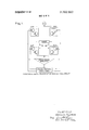
- FIG. 1 illustrates a long linear tubular metal halide lamp suitable for the invention.
- FIG. 2 compares the output distribution of the lamp of FIG. 1 under normal 60 hertz operation with that under controlled DC bias for three color bands.
- FIG. 3 is a functional block diagram of a DC bias control circuit for operating the lamp according to the invention.
- FIG. 4 shows waveform output of an operational amplifier in the control circuit.
- FIG. 5 is a detailed schematic diagram of the DC bias control circuit.
- FIG. 1 A slender tubular lamp suitable for operation according to the invention is illustrated in FIG. 1 comprising an arc tube 1 of quartz or fused silica.
- the tube may be of the size commonly referred to as T3 (tubular, it: inch dia.) having an inside diameter of about 8 millimeters and having sealed therein at opposite ends a pair of arcing electrodes 2,2 defining an arc gap of about 14 inches.
- T3 tubular, it: inch dia.
- the electrode inleads 3 have intermediate thin molybdenum foil sections 4 hermetically sealed through full diameter pinch seals 5 at the ends of the tube.
- the electrodes each comprise a double layer tungsten wire helix 6 wrapped around a tungsten core wire 7, and may be conventionally activated by thoriumoxide applied as a coating on the turns of the helix or filling the space or interstices between turns.
- quartz sleeves 8 extendingforward up to the electrode tips may be fitted over the ends of the lamp as illustrated.
- the space between the tube wall and the sleeve is filled with a refractory white insulation 9 of quartz fibers.
- FIG. 2 shows the output distribution for normal 60 hertz operation (dashed lines), and for operation with a controlled DC bias (solid lines) according to the invention, for the three color bands green, red and blue.
- the intensity is plotted as ordinate against the place of measurement along the length of the lamp as abscissa, and the improvement in uniformity is apparent.
- Operation with DC bias control permits the use of a greater variety of metal halides with more flexibility in the choice of spectral output. It reduces the need for close control of arc chamber parameters, thereby lowering the cost of manufacture and the shrinkage rate. It permits the use of very small chamberdiameters in linear lamps, for example in applications requiring critical focusing.
- FIG. 3 illustrates one scheme for controlling a DC bias current to regulate the spectral distribution of a metal halide discharge lamp.
- pair of photo sensors P1 and P2 responsive to light intensity are aimed at opposite ends of the lamp. Their signals are fed to a differential operational amplifier connected as a zero crossing detector. The output voltage of the operational amplifier is supplied to power control amplifiers which provide an on signal to the right or left upper transistor power switches (LUS or RUS), and to the diagonally opposite lower transistor power switch (RLS or LLS). The four transistor power switches determine the direction in which the DC supply current is allowed to flow through the lamp load.
- Photosensors P1 and P2 comprise photo transistors Q1 and Q2 aimed or optically coupled to receive radiation f ,f,, from opposite ends of the lamp 1. They determine the input voltage to the darlington photo amplifiers, 03,4 and Q5 ,0. To compensate for variation between the response of individual photo transistors to light flux, a sensitivity adjustment of the gain and output voltage level of the photo amplifiers is made by means of variable resistors R1 and R2 (of 50 kilohms) and R3 and R4 of 5 kilohms. The sensitivityadjustment also determines the overall response of the system to an imbalance of light at the lamp ends. It is adjusted to provide sufficiently fine control to meet the need for uniformity but not so high as to cause hunting or oscillation of the end to end light difference.
- the output of the photo amplifiers is combined with an alternating sine wave voltage from source AC and applied to the input terminals x and y of a conventional operational amplifier 0A connected as 'a zero crossing detector. If the input at terminal at exceeds that at terminal y, the output is negative;.if the input at terminal y exceeds that at terminal 1:, the output is positive.
- the control function is developed as follows.
- the input signal to the operational amplifier is the difference in voltage applied to terminals x and y and is given by:
- V, V,, Vsin wt+(V V where V sin wt is the alternating sine wave voltage from source AC, V, is the signal at x-due to sensor P1, and V is the signal at y'due to sensor P2.
- V V the input voltage to 0A is as shown in FIG. 4a.
- the output is negative, as shown in FIG. 4b and vice versa.
- V V then OA simply performs a squaring function on the input sine wave, as shown in FIG. 40.
- V V the input voltage is as shown in FIG. 4d, and the output voltage as shown in FIG. 4e.
- V is the peak of the sine wave
- At is the positive wave duration
- At is the negative wave duration. Its value can vary continuously from +V to V,, depending on the difference in the light output between the lamp ends.
- the control voltage must operate to balance the light output from opposite ends of the lamp.
- a dc voltage applied to the lamp will cause the light to increase at the cathode or negative end.
- the control circuitry must provide current through the lamp in a direction to counteract the sensed imbalance 'by reversing the dccomponent of current.
- a bridge circuit controls current flow from a constant current dc source 11.
- the bridge comprises four transistor power switches LUS, RUS, LLS and RLS, being left and right, upper and lower switches.
- the polarity of power application is determined by having LUS and RLS on at the same time as RUS and LLS are off, and vice versa.
- LUS andRLS, nor LLS and RLS should ever be on simultaneously, and it is desirable that the transition from one'polarity to, the other be made as rapidly as possible.
- Transistor 07 is a very high gain transistor and serves to increase the level of the output from operational amplifier CA as well as to speed up the voltage reversal rate to approximately 20,000 volt/sec.
- Transistor Q8 inverts the output of Q7, that is reverses its phase. Transistors 07 and Q8 thus provide the out of phase on and off control signals necessary to obtain the proper application of power to the lamp through the power switches.
- Transistors 09,10 and 011,12 provide high peak power capacity for driving the principal drive transistors 013,14 and 015,16 as rapidly as possible.
- the associated circuitry provides isolated control of the tum on and turn off signals to maximize the speed and at the same time maintaining a very low dissipation. This permits lower cost low power transistors to be used for the drive transistors.
- upper power switches LUS and RUS have individual low voltage bias supplies consisting of the full wave rectified output of transformers T and T and the bias control transistors 017 and 018.
- the lower power switches LLS and RLS operate from a single bias supply (not shown) with similar circuitry connected to terminals 12 and 13. These bias supplies insure that the power switches are in saturation at the maximum current level required for the lamp.
- the principal drive transistors are connected to the base circuit of the bias control transistors 017,18 and 019,20 and when on remove the base drive from the power switch circuits.
- a problem with such circuitry arises from the fact that transistors turn on much more rapidly than 0 and turn off from saturation can be even longer due to stored charge in the transistors (storage time). Since LUS and LLS must never be on simultaneously (similarly RUS and RLS), the turn on of these transistors must. be made slower than the turn off including storage time, the reverse of the inherent tendency. While delay networks can be used, they become complicated and result in high dissipation in the power switches when long time periods are involved.
- the darlington connection .results in much longer charge storage and slower turn OK because the conventional means of charge removal consisting in reverse biasing the emitter-base junction, cannot be used.
- this handicap is overcome by means of pulldown diodes.
- the diodes D1, D2-5; D6, D740; D11, D12-15; and D16, D17-20 provide paths for removal of stored charge from each of the transistors through the principal drive transistors and thus serve to minimize the storage time.
- the improvement in performance is remarkable: typical storage time without these diodes is 20 microseconds or more; with the pulldown diodes, it is on the order of 2.5 microseconds.
- the problem is minimized.
- the transition In square wave operation, the transition must be sufiiciently rapid to limit the reignition voltage to the capa' bility of the dc power source. Transition times of the order of 20-30 microseconds can result in reignition voltages of -200 volts and can cause difficulty in the design of the power source. Therefore it is desirable to make the transition time less than 20 microseconds,
- a circuit for overcoming nonuniformity of radiant output along the length of an elongated metal vapor discharge lamp of a kind subject to electrophoretic effects comprising:
- sensing means responsive to unbalance in spectral output between the ends of said lamp
- control means responsive to said sensing means and providing current through said lamp with a dc component proportioned to create an electrophoretic effect overcoming said unbalance.
- a lamp as in claim 1 wherein said control means providescyclic reversals of current through said lamp in addition to said dc component.
- sensing means comprises a pair of radiation sensors optically coupled to opposite ends of said lamp, said source provides a controlled dc current, and said means for connecting the lamp across said source comprises a bridge circuit including four semiconductor switches controlled by said control means in pairs to determine the direction of current flow through said lamps.
- a circuit for overcoming nonuniformity of radiant output along the length of an elongated metal vapor 8. lamp of a kind subject to electrophoretic effects, comprising:
- I a bridge circuit comprising four semiconductor switches, 7 said source being connected across one diagonal of said bridge,- 7 terminals for connecting said lamp across the other diagonal of said bridg a pair of radiation sensors optically coupled to opposite ends of said lamp and responsive to the unbalance in spectral output therefrom,
- control means cyclically turning on” and off opposite pairs of said switches in order to provide alternating current flowfrom said source through said lamp
- control means being responsive to the signals from said sensors by varying the time of current flow in any one polarity in accordance with the direction and degree of unbalance in the spectral 8.
- said control means comprises an ac source and an operational amplifier, said operational amplifier providing a square wave output reversing at the frequency of said ac source with a ratio of time duration in opposite polarities following I the degree of unbalance in the spectral output.
- each of the four switches comprises two transistors connected emitter to base with common collectors in the darlington mode, and diodes connecting the bases of said transistors to said control means in order to achieve fast removal of stored carriers at turn off.
- control means comprises an ac source and an operational amplifier, said operational amplifier providing a square wave output reversing at the frequency of said ac source with a ratio of time duration in opposite polarities following the degree of unbalance in the spectral output, and each of the four switches comprises two transistors connected emitter to base with common collectors in the darlington mode, and diodes connecting the bases of said transistors to said control means in order to achieve fast removal of stored carriers at turn off.
Abstract
A major difficulty with long linear metal halide type lamps is nonuniformity of light output along the axis of the lamp. The extent of nonuniformity increases with the number of metals included in the lamp filling and the factors primarily responsible for it are cataphoresis and thermal gradients. The cataphoretic effect is the stronger and the nonuniformity may be overcome by supplying a DC component to the discharge current and controlling its polarity and magnitude. In one system, the lamp is operated from a DC power supply through a control circuit using semi-conductors for polarity reversing switches wherein the time of current flow in one polarity is determined by the direction and degree of unbalance of the spectral output.
Description
United States Patent Lak [451 Oct. 24, 1972 [54] METAL HALIDE LAMP SYSTEM Primary Examiner-J0hn Kominski [72] Inventor: William H. Lake, Novelty, Ohio Amway-Ems [73] Assignee: General Electric Company [57] ABSTRACT [22] Filed: Sept. 23, 1971 A major difficulty with long linear metal halide type lamps is nonuniformity of light output along the axis [21] Appl' 183o94 of the lamp. The extent of nonuniformity increases with the number of metals included in the lamp filling [52] US. Cl. ..315/l5l, 250/205, 250/226, and the factors primarily responsible for it are 313/229, 315/155, 315/158, 323/21 cataphoresis and thermal gradients. The cataphoretic [51] Int. Cl. ..H05b 37/02 effect is the stronger and the nonuniformity may b 58 Field of Search ..315/l5l, 158, 155; 250/205, Overcome y pp y a DC component to the 25002 323 21; 313 discharge current and controlling its polarity and magnitude. In one system, the lamp is operated from a DC [56] References Cited power supply through a control circuit using semi-conductors for polarity reversing switches wherein the UNITED STATES PATENTS time of current flow in one polarity is determined by 2,749,501 6/1956 Bartlett ..315/158 g i i and degree unbalance the spectral 3,431,427 3/1969 Pahl, Jr ..3l5/151 10 Claims, 5 Drawing Figures LUS & pus r- 9*- *EEF LLS p p ELS OPERA TIONHL flMPL/F/EE POWER CON T201. AMPLIFIERS FUNCTIONAL BLOCK D/flGEflM 0F 176 8/95 CONT/POL C/ECU/ T PHENTED 24 I972 3 700 960 sum 1 0F 4 CONTROLLED DC Bms U) E h E L x GREEN BHND (Th'flLL um) i CONTROLLED Fig 2.3 Q DC 3/05 {5 \//-60HZ SINE WAVE S x-*- RED BHND (L/rH/L/M) 1; CONTROLLED 0 DC 3/95 E k E x BLUE BEND (IND/UM) SPECTEflL DISTRIBUTION OFLflMP TYPE 1 lnven t'or: WiLLiam H. Lake Hi5 AtTOTTWGH PATENTED 24 I97? 3. 700.960
LUS BUS LL$ p1 p2 ELS OPE? T/0NOL HMPL/F/EE POM/2 CONTROL L 4 AMPLIFIERS FUNCTIONHL BLOC/J D/flGEflM 0F DC 8/05 CON TEOL C IECU/ T lnven tow': WiLLiam H. Lake His A t t they PATENTEDCBT 24 m2 SHEEI W 0F 4 lnven tow': WiLLiam H. Lake by W I His A t tovneg BACKGROUND OF TI-IE INVENTION Long linear metal halide lamps may be designed to provide radiation in a wide variety of spectral bands as required by the particular use. Examples of industrial applications are diazo printing requiring peak output in the 3500 to 4000 A regiomphoto polymerization reactions primarily sensitive in the 2000 to 2500 A region, polymerization of photo resists in the region below 2000 A,'paint drying and air curing of coatings in the range of 2500 to 4000 A. Radiation efiiciencies of metal halide lamps specifically designed to emit in selected wavelength regions may be several times higher in those regions than other types of discharges.
An example of a long linear metal halide lamp of the kind in question is that described and claimed in copending application Ser. No. 863,732, filed July 7, 1969, now abandoned by John M. Sato, William H. Lake and Delmar D. Kershaw, entitled Selective Spectral Output Metal Halide Lamp and assigned to the same assignee as the present invention. One lamp specifically described therein for use in reprographic applications to make colored copies has radiation concentrated in the three primary colors, blue, green and red utilizes a filling of zinc, lithium and thallium iodides plus mercury.
In general, photochemical processes have photonlimited reaction rates and some specific reactions may be inhibited by radiation in other regions of the spectrum. This means that very high power densities in specific spectral regions are desirable. Long linear or slender lamps facilitate focusing of individual units as desired and also permit mounting in a closely packed array to provide very high power densities. By slender lamps are meant lamps in which the length is at least times the envelope diameter. However, slender discharge lamps tend to have the undesirable characteristic of nonuniformity of radiation along the axis of the lamp. U.S. Pat. No. 2,761,086 Noel and Falconer, August 1956, Electric Discharge Lamp, provided a solution to this problem for the case of high pressure mercury'vapor lamps emitting at 3650 A. The problem of nonuniformity is very much aggravated with metal halide lamps containing more than one metal. In such lamps the spectral output distribution becomes nonuniform along the axis, that is the color varies drastically along the length of the lamp. Unless the nonuniformity can be eliminated, the lamp is useless for reprographic applications. The degree of nonuniformity depends upon the particular metal halides used and limits the number and permissible amount of suitable materials. In addition arc chamber parameters must be carefully controlled in order to assure that lamps have a uniform spectral distribution even for acceptable metal halides. In all cases, a practical limitation exists on the length of the discharge which can be achieved without developing spectral nonuniformity.
By way of example, metal halide discharges in T3 (tubular inch arc tubes longer than 4 inches show in general at least 10 percent variation in spectral output from end to end and often as much as 100 percent when operated on alternating current. When the same lamps are operated on direct current, even greater nonuniformity results with vapor species being pumped to one end or the other of the tube by electrophoresis.
The direction and degree of pumping varies with the particular metal halide species and with the other metals present in the arc tube.
SUMMARY OF THE INVENTION 1 have found that the factors primarily responsible for nonuniformity are thermal gradients and cataphoresis. In AC discharges thermal gradients may be caused by a non-uniform bulb temperature distribution, or be variations in bulb diameter, or by unbalanced electrode losses. Regenerative conditions may exist causing small unbalances to lead to large nonuniforrnities. Cataphoresis may result directly from the nature of the current used, for instance where the current is DC or where the current is AC which includes a DC component. Cataphoresis may also result from an unbalance in the electrode energy input which effectively creates a DC component.
I have found that the electrophoretic effects resulting from the introduction of a direct component into the lamp current are fast acting and relatively powerful. By introducing a controlled DC component into the lamp operating current, the effects of the relatively weak phenomena due to thermal gradients may be overridden. The nonuniformity may be regulated and effectively overcome by controlling the direction and magnitude of the DC component introduced into the discharge current.
There are various ways in which the DC component may be supplied and controlled. One way, which may be referred to as Variable Time Ratio Square Wave Operation, operates the lamp from a DC power supply through polarity reversing switches in the form of semiconductors. A control circuit is provided whereby the time of current flow in any one polarity is determined by the direction and degree of unbalance in the spectral output.
In another circuit which may be referred to Audio Frequency with DC Offset Current, the lamp is operated directly from a high audio frequency power supply. An auxiliary control provides a parallel DC offset current to regulate the electro-phoretic effect in the lamp.
DESCRIPTION OF DRAWINGS FIG. 1 illustrates a long linear tubular metal halide lamp suitable for the invention.
FIG. 2 compares the output distribution of the lamp of FIG. 1 under normal 60 hertz operation with that under controlled DC bias for three color bands.
FIG. 3 is a functional block diagram of a DC bias control circuit for operating the lamp according to the invention.
FIG. 4 shows waveform output of an operational amplifier in the control circuit.
FIG. 5 is a detailed schematic diagram of the DC bias control circuit.
DETAILED DESCRIPTION Lamp Structure A slender tubular lamp suitable for operation according to the invention is illustrated in FIG. 1 comprising an arc tube 1 of quartz or fused silica. The tube may be of the size commonly referred to as T3 (tubular, it: inch dia.) having an inside diameter of about 8 millimeters and having sealed therein at opposite ends a pair of arcing electrodes 2,2 defining an arc gap of about 14 inches. In the drawing, portions of the lamp have been cut away to shorten the figure. The electrode inleads 3 have intermediate thin molybdenum foil sections 4 hermetically sealed through full diameter pinch seals 5 at the ends of the tube. The electrodes each comprise a double layer tungsten wire helix 6 wrapped around a tungsten core wire 7, and may be conventionally activated by thoriumoxide applied as a coating on the turns of the helix or filling the space or interstices between turns. In order to heat the. end chambers and thus increase the vapor pressure of the metal iodides, quartz sleeves 8 extendingforward up to the electrode tips may be fitted over the ends of the lamp as illustrated. The space between the tube wall and the sleeve is filled with a refractory white insulation 9 of quartz fibers.
EXAMPLE 1 In one set of lamps utilizing the above-described envelope, the filling consisted of the following:
Thallium Iodide 10 mg Lithium Iodide 5 mg Indium Iodide l0 mg Mercury 7 mg Argon torr Green 50004500 A Red 6100-6800 A Blue Under conventional sine wave alternating current operation, it was possible to maintain spectral uniformity with the above lamp filling in arc lengths up to about 10 inches. However this required close control of the arc chamber diameter, namely limiting variations in diameter to less than 10 microns per centimeter of length, close control of wall thickness, and close regulation of end chamber temperature. When the same lamps were operated utilizing a DC bias control circuit in accordance with the invention, satisfactory spectral uniformity was achieved for 14 inches are length lamps even when no attempt was made to control the important arc chamber parameters. FIG. 2 shows the output distribution for normal 60 hertz operation (dashed lines), and for operation with a controlled DC bias (solid lines) according to the invention, for the three color bands green, red and blue. In each case the intensity is plotted as ordinate against the place of measurement along the length of the lamp as abscissa, and the improvement in uniformity is apparent.
EXAMPLE 2 In a second lamp type utilizing an envelope similar to that previously described, the filling consisted of the following:
Thallium Iodide 10 mg Lithium Iodide l0 mg zinc iodide 10 mg Mercury 7 mg Argon 25 torr 14 inches.
Operation with DC bias control permits the use of a greater variety of metal halides with more flexibility in the choice of spectral output. It reduces the need for close control of arc chamber parameters, thereby lowering the cost of manufacture and the shrinkage rate. It permits the use of very small chamberdiameters in linear lamps, for example in applications requiring critical focusing.
BLOCK DIAGRAM The block diagram of FIG. 3 illustrates one scheme for controlling a DC bias current to regulate the spectral distribution of a metal halide discharge lamp. A
pair of photo sensors P1 and P2 responsive to light intensity are aimed at opposite ends of the lamp. Their signals are fed to a differential operational amplifier connected as a zero crossing detector. The output voltage of the operational amplifier is supplied to power control amplifiers which provide an on signal to the right or left upper transistor power switches (LUS or RUS), and to the diagonally opposite lower transistor power switch (RLS or LLS). The four transistor power switches determine the direction in which the DC supply current is allowed to flow through the lamp load.
Circuit Description A circuit operating in accordance with the foregoing scheme is shown schematically in FIG. 4. Photosensors P1 and P2 comprise photo transistors Q1 and Q2 aimed or optically coupled to receive radiation f ,f,, from opposite ends of the lamp 1. They determine the input voltage to the darlington photo amplifiers, 03,4 and Q5 ,0. To compensate for variation between the response of individual photo transistors to light flux, a sensitivity adjustment of the gain and output voltage level of the photo amplifiers is made by means of variable resistors R1 and R2 (of 50 kilohms) and R3 and R4 of 5 kilohms. The sensitivityadjustment also determines the overall response of the system to an imbalance of light at the lamp ends. It is adjusted to provide sufficiently fine control to meet the need for uniformity but not so high as to cause hunting or oscillation of the end to end light difference.
The output of the photo amplifiers is combined with an alternating sine wave voltage from source AC and applied to the input terminals x and y of a conventional operational amplifier 0A connected as 'a zero crossing detector. If the input at terminal at exceeds that at terminal y, the output is negative;.if the input at terminal y exceeds that at terminal 1:, the output is positive.
The control function is developed as follows. The input signal to the operational amplifier is the difference in voltage applied to terminals x and y and is given by:
V, V,,= Vsin wt+(V V where V sin wt is the alternating sine wave voltage from source AC, V, is the signal at x-due to sensor P1, and V is the signal at y'due to sensor P2. By design, the ac sine wave voltage is always greater than the difference in sensor voltages V V Then when V V the input voltage to 0A is as shown in FIG. 4a. When the input to 0A is positive, the output is negative, as shown in FIG. 4b and vice versa. When V V then OA simply performs a squaring function on the input sine wave, as shown in FIG. 40. When V V the input voltage is as shown in FIG. 4d, and the output voltage as shown in FIG. 4e.
The-average output voltage V out of operational am- 'where T= l/w period of the input sine wave, V is the peak of the sine wave, At, is the positive wave duration, and At is the negative wave duration. Its value can vary continuously from +V to V,, depending on the difference in the light output between the lamp ends.
The control voltage must operate to balance the light output from opposite ends of the lamp. For the lamp of Example 2 above, a dc voltage applied to the lamp will cause the light to increase at the cathode or negative end. The control circuitry must provide current through the lamp in a direction to counteract the sensed imbalance 'by reversing the dccomponent of current.
Referring to FIG. 5, a bridge circuit controls current flow from a constant current dc source 11. The bridge comprises four transistor power switches LUS, RUS, LLS and RLS, being left and right, upper and lower switches. The polarity of power application is determined by having LUS and RLS on at the same time as RUS and LLS are off, and vice versa. For reliability, neither LUS andRLS, nor LLS and RLS should ever be on simultaneously, and it is desirable that the transition from one'polarity to, the other be made as rapidly as possible. These requirements are fulfilled by the drive circuitry intervening between operational amplifier 0A and the transistor power switches.
Drive Circuitry Transistor 07 is a very high gain transistor and serves to increase the level of the output from operational amplifier CA as well as to speed up the voltage reversal rate to approximately 20,000 volt/sec. Transistor Q8 inverts the output of Q7, that is reverses its phase. Transistors 07 and Q8 thus provide the out of phase on and off control signals necessary to obtain the proper application of power to the lamp through the power switches.
6 In the absence of any drive sigials, all the power switches are biased off by the passive bias supplies. The
upper power switches LUS and RUS have individual low voltage bias supplies consisting of the full wave rectified output of transformers T and T and the bias control transistors 017 and 018. The lower power switches LLS and RLS operate from a single bias supply (not shown) with similar circuitry connected to terminals 12 and 13. These bias supplies insure that the power switches are in saturation at the maximum current level required for the lamp.
The principal drive transistors are connected to the base circuit of the bias control transistors 017,18 and 019,20 and when on remove the base drive from the power switch circuits. A problem with such circuitry arises from the fact that transistors turn on much more rapidly than 0 and turn off from saturation can be even longer due to stored charge in the transistors (storage time). Since LUS and LLS must never be on simultaneously (similarly RUS and RLS), the turn on of these transistors must. be made slower than the turn off including storage time, the reverse of the inherent tendency. While delay networks can be used, they become complicated and result in high dissipation in the power switches when long time periods are involved. In particular, the darlington connection .results in much longer charge storage and slower turn OK because the conventional means of charge removal consisting in reverse biasing the emitter-base junction, cannot be used. According to an important feature of the invention, this handicap is overcome by means of pulldown diodes.
The diodes D1, D2-5; D6, D740; D11, D12-15; and D16, D17-20 provide paths for removal of stored charge from each of the transistors through the principal drive transistors and thus serve to minimize the storage time. The improvement in performance is remarkable: typical storage time without these diodes is 20 microseconds or more; with the pulldown diodes, it is on the order of 2.5 microseconds.
1 The addition of very small capacitors Cl,2,3,4; delays the turn on time up to about 3 microseconds without seriously affecting the rise time and increasing thedissipation. The diode strings D2l-24 and D25-28 provide a convenient means of establishing a negative turn off bias for maximizing the turn off rate of the lower transistors. The upper transistors do not need this because they turn off into the +DC power source which provides ample pulldown drive. Lamp-Circuit Functional Considerations The reignition voltage of the long linear metal halide lamps used with this system can be extremely high. For 60 hz sine wave operation, reignition voltages greater than 2000 volts are often observed during the starting period, and greater than 1000 volts during normal operation. High reignition voltages make ballasting difficult. However with dc or square wave operation as provided by the invention, the problem is minimized. In square wave operation, the transition must be sufiiciently rapid to limit the reignition voltage to the capa' bility of the dc power source. Transition times of the order of 20-30 microseconds can result in reignition voltages of -200 volts and can cause difficulty in the design of the power source. Therefore it is desirable to make the transition time less than 20 microseconds,
and transition times on the order of 2 to l0.
microseconds, as achieved by this circuit, are much preferable. Thus avoidance of high reignition voltages is another advantage of the circuit according to the in vention.
What I claim as new and desire Patent of the US. is:'-
1. A circuit for overcoming nonuniformity of radiant output along the length of an elongated metal vapor discharge lamp of a kind subject to electrophoretic effects, comprising:
a source of electric current and means for connecting the lamp across said source,
sensing means responsive to unbalance in spectral output between the ends of said lamp,
and control means responsive to said sensing means and providing current through said lamp with a dc component proportioned to create an electrophoretic effect overcoming said unbalance.
2. A lamp as in claim 1 wherein said control means providescyclic reversals of current through said lamp in addition to said dc component.
to secure by Letters 3. A circuit as in claim 1 wherein said sensing means 7 comprises a pair of radiation sensors optically coupled to opposite ends of said lamp.
4. A circuit as in claim 1 wherein said source provides a controlled dc current and said means for connecting the lamp across said source comprises semiconductor switches controlled by said control means.
5. A circuit as in claim 1 wherein said source provides a controlled dc currentand said means for connecting the lamp across said source comprises a bridge circuit including four semi-conductor switches controlled by said control means in pairs to determine the direction of current flow through said lamps.
6. A circuit as in claim 1 wherein said sensing means comprises a pair of radiation sensors optically coupled to opposite ends of said lamp, said source provides a controlled dc current, and said means for connecting the lamp across said source comprises a bridge circuit including four semiconductor switches controlled by said control means in pairs to determine the direction of current flow through said lamps.
7. A circuit for overcoming nonuniformity of radiant output along the length of an elongated metal vapor 8. lamp of a kind subject to electrophoretic effects, comprising:
a source of controlled electric dc current,
I a bridge circuit comprising four semiconductor switches, 7 said source being connected across one diagonal of said bridge,- 7 terminals for connecting said lamp across the other diagonal of said bridg a pair of radiation sensors optically coupled to opposite ends of said lamp and responsive to the unbalance in spectral output therefrom,
control means cyclically turning on" and off opposite pairs of said switches in order to provide alternating current flowfrom said source through said lamp,
said control means being responsive to the signals from said sensors by varying the time of current flow in any one polarity in accordance with the direction and degree of unbalance in the spectral 8. lil iic itit as in claim 7 wherein said control means comprises an ac source and an operational amplifier, said operational amplifier providing a square wave output reversing at the frequency of said ac source with a ratio of time duration in opposite polarities following I the degree of unbalance in the spectral output.
9. A circuit as in claim 7 wherein each of the four switches comprises two transistors connected emitter to base with common collectors in the darlington mode, and diodes connecting the bases of said transistors to said control means in order to achieve fast removal of stored carriers at turn off.
10. A circuit as in claim 7 wherein said control means comprises an ac source and an operational amplifier, said operational amplifier providing a square wave output reversing at the frequency of said ac source with a ratio of time duration in opposite polarities following the degree of unbalance in the spectral output, and each of the four switches comprises two transistors connected emitter to base with common collectors in the darlington mode, and diodes connecting the bases of said transistors to said control means in order to achieve fast removal of stored carriers at turn off.
UNITED STATES PATENT orrmr QERTEFEQATE M CQRREQTEGN Patent NO. 3,700,960 Dated October 24, 1972 Inventor(s) WILLIAM H. LAKE It is certified that error appears in the above-identified patent and that said Letters Patent are hereby corrected as shown below:
218,491, filed January 17, 1972,
Signed and sealed this 20th fiay of November 1973.
(SEAL) Attest 2 EDWARD Ni.FlZ-FIICHER ,3B5.a RENE D. 'JE'EGTMEYER Attesting Officer Acting Commissioner of Patents FORM P0-1050 (10-69) UscOMM. 375.p69
# U.S. GQVERNMENT PRlNTING OFFICE: I989 O-366-334.
Claims (10)
1. A circuit for overcoming nonuniformity of radiant output along the length of an elongated metal vapor discharge lamp of a kind subject to electrophoretic effects, comprising: a source of electric current and means for connecting the lamp across said source, sensing means responsive to unbalance in spectral output between the ends of said lamp, and control means responsive to said sensing means and providing current through said lamp with a dc component proportioned to create an electrophoretic effect overcoming said unbalance.
2. A lamp as in claim 1 wherein said control means provides cyclic reversals of current through said lamp in addition to said dc component.
3. A circuit as in claim 1 wherein said sensing means comprises a pair of radiation sensors optically coupled to opposite ends of said lamp.
4. A circuit as in claim 1 wherein said source provides a controlled dc current and said means for connecting the lamp across said source comprises semiconductor switches controlled by said control means.
5. A circuit as in claim 1 wherein said source provides a controlled dc current and said means for connecting the lamp across said source comprises a bridge circuit including four semi-conductor switches controlled by said control means in pairs to determine the direction of current flow through said lamps.
6. A circuit as in claim 1 wherein said sensing means comprises a pair of radiation sensors optically coupled to opposite ends of said lamp, said source provides a controlled dc current, and said means for connecting the lamp across said source comprises a bridge circuit including four semiconductor switches controlled by said control means in pairs to determine the direction of current flow through said lamps.
7. A circuit for overcoming nonuniformity of radiant output along the length of an elongated metal vapor lamp of a kind subject to electrophoretic effects, comprising: a source of controlled electric dc current, a bridge circuit comprising four semiconductor switches, said source being connected across one diagonal of said bridge, terminals for connecting said lamp across the other diagonal of said bridge, a pair of radiation sensors optically coupled to opposite ends of said lamp and responsive to the unbalance in spectral output therefrom, control means cyclically turning ''''on'''' and ''''off'''' opposite pairs of said switches in order to provide alternating current flow from said source through said lamp, said control means being responsive to the signals from said sensors by varying the time of current flow in any one polarity in accordance with the direction and degree of unbalance in the spectral output.
8. A circuit as in claim 7 wherein said control means comprises an ac source and an operational amplifier, said operational amplifier providing a square wave output reversing at the frequency of said ac source with a ratio of time duration in opposite polarities following the degree of unbalance in the spectral output.
9. A circuit as in claim 7 wherein each of the four switches comprises two transistors connected emitter to base with common collectors in the darlington mode, and diodes connecting the bases of said transistors to said control means in order to achieve fast removal of stored carriers at turn off.
10. A circuit as in claim 7 wherein said control means comprises an ac source and an operational amplifier, said operational amplifier providing a square wave output reversing at the frequency of said ac source with a ratio of time duration in opposite polarities following the degree of unbalance in the spectral output, and each of the four switches comprises two transistors connected emitter to base with common collectors in the darlington mode, and diodes connecting the bases of said transistors to said control means in order to achieve fast removal of stored carriers at turn off.
Applications Claiming Priority (1)
| Application Number | Priority Date | Filing Date | Title |
|---|---|---|---|
| US18309471A | 1971-09-23 | 1971-09-23 |
Publications (1)
| Publication Number | Publication Date |
|---|---|
| US3700960A true US3700960A (en) | 1972-10-24 |
Family
ID=22671417
Family Applications (1)
| Application Number | Title | Priority Date | Filing Date |
|---|---|---|---|
| US183094A Expired - Lifetime US3700960A (en) | 1971-09-23 | 1971-09-23 | Metal halide lamp system |
Country Status (6)
| Country | Link |
|---|---|
| US (1) | US3700960A (en) |
| JP (1) | JPS4841565A (en) |
| CA (1) | CA1031407A (en) |
| DE (1) | DE2246234A1 (en) |
| FR (1) | FR2153366A1 (en) |
| NL (1) | NL7212886A (en) |
Cited By (16)
| Publication number | Priority date | Publication date | Assignee | Title |
|---|---|---|---|---|
| US3892961A (en) * | 1973-03-21 | 1975-07-01 | Intermadox A G | Contactless potentiometer with automatically controlled light source |
| US3904922A (en) * | 1973-11-19 | 1975-09-09 | Xerox Corp | Lamp control and lamp switch circuit |
| US3909609A (en) * | 1973-10-29 | 1975-09-30 | Xerox Corp | Light source measuring apparatus |
| US3993899A (en) * | 1973-12-13 | 1976-11-23 | Gunson's Sortex Limited | Sorting machine with fiber optic focusing means |
| US4004188A (en) * | 1975-09-26 | 1977-01-18 | General Electric Company | Starting circuit for inverter operated gaseous discharge lamps |
| DE2636876A1 (en) * | 1975-08-21 | 1977-02-24 | Mitsubishi Electric Corp | METHOD FOR MIXED LIGHTING |
| US4012663A (en) * | 1974-11-25 | 1977-03-15 | General Electric Company | Lighting control system |
| DE2707987A1 (en) * | 1976-02-27 | 1977-09-15 | Mitsubishi Electric Corp | LIGHTING PROCESS FOR THE FORMATION OF COLORED SHADOWS |
| US4190795A (en) * | 1977-09-09 | 1980-02-26 | Coberly & Associates | Constant intensity light source |
| US4360756A (en) * | 1979-11-13 | 1982-11-23 | General Electric Company | Metal halide lamp containing ThI4 with added elemental cadmium or zinc |
| US4697709A (en) * | 1985-09-03 | 1987-10-06 | Delta Technology Corporation | Sorter for agricultural products |
| US4803406A (en) * | 1984-11-05 | 1989-02-07 | Hitachi, Ltd. | High-pressure discharge lamp operating circuit |
| US5333034A (en) * | 1992-01-31 | 1994-07-26 | Bremson Data Systems, Inc. | System for selectively controlling the spectral make-up of visible light from a source thereof |
| US5581161A (en) * | 1994-07-13 | 1996-12-03 | Gong; Mingfu | DC coupled electronic ballast with a larger DC and smaller AC signal |
| US20040066153A1 (en) * | 2002-10-07 | 2004-04-08 | Nemirow Arthur T. | Electronic ballast with DC output flyback converter |
| US20040178746A1 (en) * | 2003-03-11 | 2004-09-16 | Bruce Industries, Inc. | Low frequency output electronic ballast |
Families Citing this family (2)
| Publication number | Priority date | Publication date | Assignee | Title |
|---|---|---|---|---|
| ZA824856B (en) * | 1981-07-28 | 1983-05-25 | Lee Electric Lighting | Power supply for arc lamps |
| JP2902272B2 (en) * | 1993-08-27 | 1999-06-07 | 株式会社三協精機製作所 | Magnetic card reader |
Citations (2)
| Publication number | Priority date | Publication date | Assignee | Title |
|---|---|---|---|---|
| US2749501A (en) * | 1950-10-06 | 1956-06-05 | California Packing Corp | Photoelectric voltage regulator |
| US3431427A (en) * | 1965-10-24 | 1969-03-04 | Henry D Pahl Jr | Solid state color balance controller for incandescent lamps |
-
1971
- 1971-09-23 US US183094A patent/US3700960A/en not_active Expired - Lifetime
-
1972
- 1972-08-15 CA CA149,424A patent/CA1031407A/en not_active Expired
- 1972-09-21 JP JP47094151A patent/JPS4841565A/ja active Pending
- 1972-09-21 DE DE2246234A patent/DE2246234A1/en active Pending
- 1972-09-21 FR FR7233436A patent/FR2153366A1/fr not_active Withdrawn
- 1972-09-22 NL NL7212886A patent/NL7212886A/xx unknown
Patent Citations (2)
| Publication number | Priority date | Publication date | Assignee | Title |
|---|---|---|---|---|
| US2749501A (en) * | 1950-10-06 | 1956-06-05 | California Packing Corp | Photoelectric voltage regulator |
| US3431427A (en) * | 1965-10-24 | 1969-03-04 | Henry D Pahl Jr | Solid state color balance controller for incandescent lamps |
Cited By (18)
| Publication number | Priority date | Publication date | Assignee | Title |
|---|---|---|---|---|
| US3892961A (en) * | 1973-03-21 | 1975-07-01 | Intermadox A G | Contactless potentiometer with automatically controlled light source |
| US3909609A (en) * | 1973-10-29 | 1975-09-30 | Xerox Corp | Light source measuring apparatus |
| US3904922A (en) * | 1973-11-19 | 1975-09-09 | Xerox Corp | Lamp control and lamp switch circuit |
| US3993899A (en) * | 1973-12-13 | 1976-11-23 | Gunson's Sortex Limited | Sorting machine with fiber optic focusing means |
| US4012663A (en) * | 1974-11-25 | 1977-03-15 | General Electric Company | Lighting control system |
| DE2636876A1 (en) * | 1975-08-21 | 1977-02-24 | Mitsubishi Electric Corp | METHOD FOR MIXED LIGHTING |
| US4004188A (en) * | 1975-09-26 | 1977-01-18 | General Electric Company | Starting circuit for inverter operated gaseous discharge lamps |
| DE2707987A1 (en) * | 1976-02-27 | 1977-09-15 | Mitsubishi Electric Corp | LIGHTING PROCESS FOR THE FORMATION OF COLORED SHADOWS |
| US4190795A (en) * | 1977-09-09 | 1980-02-26 | Coberly & Associates | Constant intensity light source |
| US4360756A (en) * | 1979-11-13 | 1982-11-23 | General Electric Company | Metal halide lamp containing ThI4 with added elemental cadmium or zinc |
| US4803406A (en) * | 1984-11-05 | 1989-02-07 | Hitachi, Ltd. | High-pressure discharge lamp operating circuit |
| US4697709A (en) * | 1985-09-03 | 1987-10-06 | Delta Technology Corporation | Sorter for agricultural products |
| US5333034A (en) * | 1992-01-31 | 1994-07-26 | Bremson Data Systems, Inc. | System for selectively controlling the spectral make-up of visible light from a source thereof |
| US5581161A (en) * | 1994-07-13 | 1996-12-03 | Gong; Mingfu | DC coupled electronic ballast with a larger DC and smaller AC signal |
| US20040066153A1 (en) * | 2002-10-07 | 2004-04-08 | Nemirow Arthur T. | Electronic ballast with DC output flyback converter |
| US6864642B2 (en) | 2002-10-07 | 2005-03-08 | Bruce Industries, Inc. | Electronic ballast with DC output flyback converter |
| US20040178746A1 (en) * | 2003-03-11 | 2004-09-16 | Bruce Industries, Inc. | Low frequency output electronic ballast |
| US6879113B2 (en) | 2003-03-11 | 2005-04-12 | Bruce Industries, Inc. | Low frequency output electronic ballast |
Also Published As
| Publication number | Publication date |
|---|---|
| DE2246234A1 (en) | 1973-03-29 |
| FR2153366A1 (en) | 1973-05-04 |
| NL7212886A (en) | 1973-03-27 |
| JPS4841565A (en) | 1973-06-18 |
| CA1031407A (en) | 1978-05-16 |
Similar Documents
| Publication | Publication Date | Title |
|---|---|---|
| US3700960A (en) | Metal halide lamp system | |
| US2624858A (en) | Gaseous discharge lamp | |
| US3117248A (en) | Low pressure mercury vapor discharge lamp for direct current operation | |
| US5949192A (en) | Operating apparatus for discharge lamp | |
| JPH0529085A (en) | Rare gas discharge lamp device | |
| US5363019A (en) | Variable color discharge device | |
| US5046152A (en) | Ignition circuit for a gas discharge lamp | |
| US3514667A (en) | Gas-filled discharge tube impulse control and operating apparatus | |
| US3603841A (en) | Fluorescent lamp device with luminosity control | |
| US3591828A (en) | Discharge lamp device and its operating apparatus | |
| SU596925A1 (en) | Ac voltage stabilizer | |
| US4340844A (en) | Lighting equipment | |
| JP2003223868A (en) | Light source device and liquid crystal display device | |
| US3543086A (en) | Impedance controlling circuit for a load element | |
| JPS61118956A (en) | Small low-pressure mercury discharge tube | |
| JP3121306B2 (en) | Inverter circuit for cold cathode discharge tube with dimming function | |
| US966205A (en) | Apparatus for transforming electrical energy. | |
| JPS59141158A (en) | Plate-type discharge lamp device | |
| JP2600646Y2 (en) | Lighting device for discharge lamp | |
| US2403700A (en) | Mercury arc device | |
| US682691A (en) | Method of operating electric lamps. | |
| JPH0696879A (en) | Power supply unit for driving cathode discharge tube | |
| JPH0410393A (en) | Lighting device for noble gas discharge lamp | |
| JP2800418B2 (en) | How to activate a mercury dispenser | |
| US1188575A (en) | Single-phase gas or vapor electric device. |