US3290567A - Controlled deposition and growth of polycrystalline films in a vacuum - Google Patents
Controlled deposition and growth of polycrystalline films in a vacuum Download PDFInfo
- Publication number
- US3290567A US3290567A US511285A US51128565A US3290567A US 3290567 A US3290567 A US 3290567A US 511285 A US511285 A US 511285A US 51128565 A US51128565 A US 51128565A US 3290567 A US3290567 A US 3290567A
- Authority
- US
- United States
- Prior art keywords
- gowen
- growth
- vacuum
- controlled deposition
- polycrystalline films
- Prior art date
- Legal status (The legal status is an assumption and is not a legal conclusion. Google has not performed a legal analysis and makes no representation as to the accuracy of the status listed.)
- Expired - Lifetime
Links
Images


Classifications
-
- C—CHEMISTRY; METALLURGY
- C23—COATING METALLIC MATERIAL; COATING MATERIAL WITH METALLIC MATERIAL; CHEMICAL SURFACE TREATMENT; DIFFUSION TREATMENT OF METALLIC MATERIAL; COATING BY VACUUM EVAPORATION, BY SPUTTERING, BY ION IMPLANTATION OR BY CHEMICAL VAPOUR DEPOSITION, IN GENERAL; INHIBITING CORROSION OF METALLIC MATERIAL OR INCRUSTATION IN GENERAL
- C23C—COATING METALLIC MATERIAL; COATING MATERIAL WITH METALLIC MATERIAL; SURFACE TREATMENT OF METALLIC MATERIAL BY DIFFUSION INTO THE SURFACE, BY CHEMICAL CONVERSION OR SUBSTITUTION; COATING BY VACUUM EVAPORATION, BY SPUTTERING, BY ION IMPLANTATION OR BY CHEMICAL VAPOUR DEPOSITION, IN GENERAL
- C23C14/00—Coating by vacuum evaporation, by sputtering or by ion implantation of the coating forming material
- C23C14/22—Coating by vacuum evaporation, by sputtering or by ion implantation of the coating forming material characterised by the process of coating
- C23C14/24—Vacuum evaporation
- C23C14/32—Vacuum evaporation by explosion; by evaporation and subsequent ionisation of the vapours, e.g. ion-plating
-
- H—ELECTRICITY
- H01—ELECTRIC ELEMENTS
- H01C—RESISTORS
- H01C10/00—Adjustable resistors
-
- H—ELECTRICITY
- H01—ELECTRIC ELEMENTS
- H01C—RESISTORS
- H01C17/00—Apparatus or processes specially adapted for manufacturing resistors
- H01C17/06—Apparatus or processes specially adapted for manufacturing resistors adapted for coating resistive material on a base
- H01C17/075—Apparatus or processes specially adapted for manufacturing resistors adapted for coating resistive material on a base by thin-film techniques
- H01C17/10—Apparatus or processes specially adapted for manufacturing resistors adapted for coating resistive material on a base by thin-film techniques by flame spraying
-
- H—ELECTRICITY
- H01—ELECTRIC ELEMENTS
- H01C—RESISTORS
- H01C17/00—Apparatus or processes specially adapted for manufacturing resistors
- H01C17/06—Apparatus or processes specially adapted for manufacturing resistors adapted for coating resistive material on a base
- H01C17/075—Apparatus or processes specially adapted for manufacturing resistors adapted for coating resistive material on a base by thin-film techniques
- H01C17/12—Apparatus or processes specially adapted for manufacturing resistors adapted for coating resistive material on a base by thin-film techniques by sputtering
Definitions
- HAMMOND E. T. GOWEN Attorney 1965 H. E. T. GOWEN CONTROLLED DEPOSITION AND GROWTH POLYCRYSTALLINE FILMS IN A VAC-UH Original Filed Sept. 25, 1960 INVENTOR.
- HAMMOND E. T. GOWEN Attorney 7M- Dec. 6, 1966 H. E. T. GOWEN 3,290,567
Landscapes
- Engineering & Computer Science (AREA)
- Microelectronics & Electronic Packaging (AREA)
- Chemical & Material Sciences (AREA)
- Manufacturing & Machinery (AREA)
- Chemical Kinetics & Catalysis (AREA)
- Materials Engineering (AREA)
- Mechanical Engineering (AREA)
- Metallurgy (AREA)
- Organic Chemistry (AREA)
- Chemical Vapour Deposition (AREA)
- Physical Vapour Deposition (AREA)
Description
Dec. 6, 1966 H. E. T. GOWEN 3,290,557
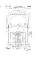
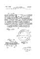
CONTROLLED DEPOSITION AND GROWTH OF POLYCRYSTALLINE FILMS IN A VACUUM Original Filed Sept. 23, 1960 21 Sheets-$heet 1 I l ""KZO j \JUU INVENTOR. HAMMOND E. T. GOWEN Attorney Dec. 6, 1966 H. E T. GOWEN 3,290,567
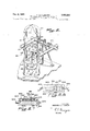
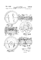
CONTROLLED DEPOSITION AND GROWTH OF POLYCRYSTALLINE FILMS IN A VACUUM Original Filed Sept. 25, 1960 21 Sheets-Sheet 2 V 2|9 W x w 1| 2:8
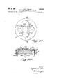
2|? 1 i .2 222 1% 6/ P /T\",-I(I/ V I J); 2'5 I am :41; f
1 220 i y 5 M w 223 2l6 K i125 2|2 2|| V O 209 2.0 207 9 208 I I I 1 5 2607 LIGHT 2609 INVENTOR. HAMMOND E. T. GOWEN Dec. 6, 1955 -r GOWEN 3,290,567
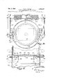
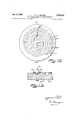
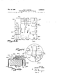
CONTROLLED DEPOSITION AND GROWTH OF POLYCRYSTALLINE FILMS IN A VACUUM Original Filed Sept. 23. 1960 21 Sheets-Sheet 3 INVENTOR. HAMMOND E. T. GOWEN Attorney 1956 H. E. T. GOWEN CONTROLLED DEPOSITION AND GROWTH OF POLYCRYSTALLINE FILMS IN A VACUUM Original Filed Sept. 23, 1960 21 Sheets-$heet =2 INVENTOR. HAMMOND E. T. GOWEN AHomey Dec. 6, 1966 H. E. T. GOWEN 3, 0,
CONTROLLED DEPOSITION AND GROWTH OF POLYCRYSTALLINE FILMS IN A VACUUM Ongmal Filed Sept. 23, 1960 21 Sheets$heet 5 v M m SCI AVA r INVENTOR. HAMMOND E. T. GOWEN BY EX Attorney Dec. 6, 1966 H. E. T. GOWEN CONTROLLED DEPOSITION AND GROWTH O FOLYCRYSTALLINE FILMS IN A VACUUM Original Filed Sept. 25, 1960 HAMMO 21 Sheets-Sheet 6 INVENTOR. ND E. T GOWEN Dec. 6, 1966 GQWEN 3,290,567
CONTROLLED DEPOSITION AND GROWTH OF FOLYCRYSTALLINE FILMS IN A VACUUM Original Filed Sept. 25, 1960 21 sheets sheet 7 INVENTOR. HAMMOND E. T. GOWEN Attorney o 4 O 7 9 6 I m w M m M AU, MW 3 NW, N W 9 0 2 m N m W 3 m u H 1 m S n W m C. f w E 1 3 v D f 2 I I 6 1 N g 0 m o E 3 M Y 9 M O A B m H w o MM H. E. T. GOWEN CONTROLLED DEPOSITION AND GROWTH OF POLYCRYSTALLINE FILMS IN A VACUUM Original Filed Sept. 23. 1960 Attorney 1966 H E. T. GOWEN 3,290,567
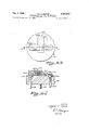
CONTROLLED DEPOSITION AND GROWTH OF POLYCRYSTALLINE FILMS IN A VACUUM Origmal Filed Sept. 23, 1960 21 Sheets$heet ll INVENTOR. HAMMOND E. T. GOW E N Attorney Dec. 6, 1966 E gow 3,290,567
H. CONTROLLED DEPOSITION AND GROWTH OF POLYGRYSTALLINE FILMS IN A VACUUM Original Filed Sept. 23, 1960 21 Sheets-Sheet 12 "5k up INVENTOR.
HAMMOND E. T. GOWEN orney Dec. 6, 1966 H. E. "r. GOWEN 3,290,567
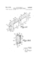
CONTROLLED DEPOSITION AND GROWTH OF POLYCRYSTALLINE FILMS IN A VACUUM Original Filed Sept. 23, 1960 21 Sheets-Sheet l3 IN V EN TOR.
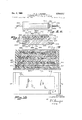
HAMMOND E.T. GOWEN Attorney Dec. 6, 1966 H. E. T. GOWEN 3,290,567 CONTROLLED DEPOSITION AND GROWTH OF POLYCRYSTALLINE FILMS IN A VACUUM Original Filed Sept. 23. 1960 21 Sheets-Sheet 14 3508 z J I 1 I I I7- f I I I 'i X/g 350i I I I, I I 1 g I, I I i" I I INVENTOR.
HAMMOND E. T. GOWEN Attorney Dec. 6, 1966 H. E. GOWEN 3,290,567
CONTROLLED DEP TION AND GR H 0F LYCRYSTALLINE FILMS IN A UUM Ongmal Filed Sept. 1960 21 Sheets-$heet 15 7 ill INVENTOR.
HAMMOND E. T. GOWEN Attorney Dec. 6, 1966 H. E. T. GOWEN CONTROLLED DEPOSITION AND GROWTH OF POLYCRYSTALLINE FILMS IN A VACUUM Original Filed Sept. 23, 1960 21 Sheets-Sheet 16 INVENTOR.
HAMMOND E. T. GOWEN Attorney Dec. 6, 1966 H E. T. GOWEN 3,290,567
CONTROLLED DEPOSITION AND GROWTH OF POLYCRYSTALLINE FILMS IN A VACUUM Original Filed Sept. 25, 1960 21 Sheets*Sheet 17 5695 505 U U U 5601 F ME E :1 W 5612 5608 D sen H 2 2 mu '1 n i l NIH 56|4 ['ll I) m inn, T C
ii g jsil m hw mm. m n n M W 5609 INVENTOR. HAMMOND E. T. GOWEN Attorney 5, 1966 H. E. 'r. GOWEN CONTROLLED DEPOSITION AND GROWTH OF POLYCRYSTALLINE FILMS IN A VACUUM Original Filed Sept. 25. 1960 21 Sheets-Sheet 18 INVENTOR.
HAMMOND E. T. GOWEN Attorney 1965 H. E. T. GOWEN CONTROLLED DEPOSITION AND GROWTH POLYCRYSTALLINE FILMS IN A VAC-UH Original Filed Sept. 25, 1960 INVENTOR. HAMMOND E. T. GOWEN Attorney 7M- Dec. 6, 1966 H. E. T. GOWEN 3,290,567
CONTROLLED DEPOSITION AND GROWTH OF POLYCRYSTALLINE FILMS IN A VACUUM Original Filed Sept. 25, 1960 21 Sl1eets-$heet 20 INVENTOR. HAMMOND E. T. GOWEN Atiorney
Claims (1)
- 6. IN AN ARTICLE OF MANUFACTURE, A SUBSTRATE, A CRYSTALLINE COATING ON SAID SUBSTRATE, SAID COATING COMPRISING A PLURALITY OF MONOCRYSTALS JOINED IN BOUNDARIES IN THE DIRECTION SUBSTANTIALLY PARALLEL TO THE SURFACE OF THE SUBSTRATE, SAID MONOCRYSTALS IN A DIRECTION AWAY FROM THE SURFACE OF SAID SUBSTRATE BEING A SINGLE CRYSTALLOGRAPHIC STRUCTURE HAVING AN INCLINATION PARALLEL TO AN AXIS OF THE
Priority Applications (2)
| Application Number | Priority Date | Filing Date | Title |
|---|---|---|---|
| US511285A US3290567A (en) | 1960-09-23 | 1965-11-16 | Controlled deposition and growth of polycrystalline films in a vacuum |
| US578290A US3371649A (en) | 1960-09-23 | 1966-09-09 | Means for controlled deposition and growth of polycrystalline films in a vacuum |
Applications Claiming Priority (2)
| Application Number | Priority Date | Filing Date | Title |
|---|---|---|---|
| US5814460A | 1960-09-23 | 1960-09-23 | |
| US511285A US3290567A (en) | 1960-09-23 | 1965-11-16 | Controlled deposition and growth of polycrystalline films in a vacuum |
Publications (1)
| Publication Number | Publication Date |
|---|---|
| US3290567A true US3290567A (en) | 1966-12-06 |
Family
ID=32396494
Family Applications (1)
| Application Number | Title | Priority Date | Filing Date |
|---|---|---|---|
| US511285A Expired - Lifetime US3290567A (en) | 1960-09-23 | 1965-11-16 | Controlled deposition and growth of polycrystalline films in a vacuum |
Country Status (1)
| Country | Link |
|---|---|
| US (1) | US3290567A (en) |
Cited By (13)
| Publication number | Priority date | Publication date | Assignee | Title |
|---|---|---|---|---|
| US3467057A (en) * | 1966-07-27 | 1969-09-16 | Hitachi Ltd | Electron beam evaporator |
| US3472679A (en) * | 1965-08-25 | 1969-10-14 | Xerox Corp | Coating surfaces |
| US3492152A (en) * | 1967-01-30 | 1970-01-27 | Gen Dynamics Corp | Method of vacuum vapor depositing a material on a substrate including reconstitution of decomposed portions of the material |
| US3575133A (en) * | 1968-04-05 | 1971-04-13 | Euratom | Apparatus for evaporation by levitation in an ultravacuum |
| US3651385A (en) * | 1968-09-18 | 1972-03-21 | Sony Corp | Semiconductor device including a polycrystalline diode |
| US3776181A (en) * | 1970-02-02 | 1973-12-04 | Ransburg Electro Coating Corp | Deposition apparatus for an organometallic material |
| US3912826A (en) * | 1972-08-21 | 1975-10-14 | Airco Inc | Method of physical vapor deposition |
| US3953619A (en) * | 1972-10-03 | 1976-04-27 | Agency Of Industrial Science & Technology | Method for ionization electrostatic plating |
| US3968270A (en) * | 1973-11-06 | 1976-07-06 | Takashi Hasegawa | Process for preparation of metal coatings |
| US4099969A (en) * | 1974-10-10 | 1978-07-11 | Xerox Corporation | Coating method to improve adhesion of photoconductors |
| WO1981003669A1 (en) * | 1980-06-13 | 1981-12-24 | Science & Techn Ets | Method for manufacturing a thin layer with orientated structure,device for implementing such method and products obtained thereby |
| US5089426A (en) * | 1985-09-21 | 1992-02-18 | Semiconductor Energy Laboratory Co., Ltd. | Method for manufacturing a semiconductor device free from electrical shortage due to pin-hole formation |
| US20090056328A1 (en) * | 2007-08-27 | 2009-03-05 | National Yang-Ming University | Micro Generator System |
-
1965
- 1965-11-16 US US511285A patent/US3290567A/en not_active Expired - Lifetime
Non-Patent Citations (1)
| Title |
|---|
| None * |
Cited By (14)
| Publication number | Priority date | Publication date | Assignee | Title |
|---|---|---|---|---|
| US3472679A (en) * | 1965-08-25 | 1969-10-14 | Xerox Corp | Coating surfaces |
| US3467057A (en) * | 1966-07-27 | 1969-09-16 | Hitachi Ltd | Electron beam evaporator |
| US3492152A (en) * | 1967-01-30 | 1970-01-27 | Gen Dynamics Corp | Method of vacuum vapor depositing a material on a substrate including reconstitution of decomposed portions of the material |
| US3575133A (en) * | 1968-04-05 | 1971-04-13 | Euratom | Apparatus for evaporation by levitation in an ultravacuum |
| US3651385A (en) * | 1968-09-18 | 1972-03-21 | Sony Corp | Semiconductor device including a polycrystalline diode |
| US3776181A (en) * | 1970-02-02 | 1973-12-04 | Ransburg Electro Coating Corp | Deposition apparatus for an organometallic material |
| US3912826A (en) * | 1972-08-21 | 1975-10-14 | Airco Inc | Method of physical vapor deposition |
| US3953619A (en) * | 1972-10-03 | 1976-04-27 | Agency Of Industrial Science & Technology | Method for ionization electrostatic plating |
| US3968270A (en) * | 1973-11-06 | 1976-07-06 | Takashi Hasegawa | Process for preparation of metal coatings |
| US4099969A (en) * | 1974-10-10 | 1978-07-11 | Xerox Corporation | Coating method to improve adhesion of photoconductors |
| WO1981003669A1 (en) * | 1980-06-13 | 1981-12-24 | Science & Techn Ets | Method for manufacturing a thin layer with orientated structure,device for implementing such method and products obtained thereby |
| US5089426A (en) * | 1985-09-21 | 1992-02-18 | Semiconductor Energy Laboratory Co., Ltd. | Method for manufacturing a semiconductor device free from electrical shortage due to pin-hole formation |
| US20090056328A1 (en) * | 2007-08-27 | 2009-03-05 | National Yang-Ming University | Micro Generator System |
| US8046993B2 (en) * | 2007-08-27 | 2011-11-01 | National Yang-Ming University | Micro generator system |
Similar Documents
| Publication | Publication Date | Title |
|---|---|---|
| US3290567A (en) | Controlled deposition and growth of polycrystalline films in a vacuum | |
| GB886393A (en) | Semiconductor body formation | |
| GB1536487A (en) | Device for displacing an egg-tray | |
| GB1525312A (en) | Distributing conveyor device | |
| GB1266677A (en) | ||
| JPS5320282A (en) | Goods picking system | |
| JPS55123176A (en) | Thin film solar cell | |
| GB814173A (en) | Improvements relating to hydrofoils for high speed marine craft | |
| US3297171A (en) | Mechanical handling apparatus | |
| US3022617A (en) | Conveyor keg palletizing device | |
| JPS5291624A (en) | High speed addition circuit | |
| GB1451668A (en) | Semiconductor manufacturing systems | |
| GB1187418A (en) | A Sheet Handling and Sampling Apparatus | |
| JPS5423302A (en) | Connecting structure between enclosures for testing devices | |
| ES442423A1 (en) | Photovoltaic devices | |
| JPS57178341A (en) | Wafer sucking device | |
| NL6917954A (en) | ||
| JPS5237790A (en) | Process for production of polycrystalline semiconductor films | |
| SU516157A1 (en) | Single Channel Phase Control Device For Valve Converter | |
| US3299438A (en) | Switching system common control | |
| Kirkpatrick et al. | A nonconventional approach to thin film cell fabrication | |
| FR2233262A1 (en) | Transferring paper etc. sheets to moving element - sheet held adjacent front edge, is moved towards moving holding element | |
| MELTON | Twenty-five years of Skyhook(Skyhook plastic balloons for transporting scientific instruments to high altitudes for long durations) | |
| US3604099A (en) | Methods of and apparatus for bonding leaded devices to substrates | |
| JPS5380160A (en) | Manufacture of substrate for semiconductor device |