US20200048773A1 - Electroless plating process - Google Patents
Electroless plating process Download PDFInfo
- Publication number
- US20200048773A1 US20200048773A1 US16/485,543 US201816485543A US2020048773A1 US 20200048773 A1 US20200048773 A1 US 20200048773A1 US 201816485543 A US201816485543 A US 201816485543A US 2020048773 A1 US2020048773 A1 US 2020048773A1
- Authority
- US
- United States
- Prior art keywords
- nickel
- film
- electroless
- plating
- electroless plating
- Prior art date
- Legal status (The legal status is an assumption and is not a legal conclusion. Google has not performed a legal analysis and makes no representation as to the accuracy of the status listed.)
- Pending
Links
- 238000000034 method Methods 0.000 title claims abstract description 151
- 238000007772 electroless plating Methods 0.000 title claims abstract description 131
- 230000008569 process Effects 0.000 title claims abstract description 118
- PXHVJJICTQNCMI-UHFFFAOYSA-N Nickel Chemical compound [Ni] PXHVJJICTQNCMI-UHFFFAOYSA-N 0.000 claims abstract description 708
- 229910052759 nickel Inorganic materials 0.000 claims abstract description 320
- 238000007747 plating Methods 0.000 claims abstract description 169
- 239000010931 gold Substances 0.000 claims abstract description 125
- RYGMFSIKBFXOCR-UHFFFAOYSA-N Copper Chemical compound [Cu] RYGMFSIKBFXOCR-UHFFFAOYSA-N 0.000 claims abstract description 93
- 229910052802 copper Inorganic materials 0.000 claims abstract description 93
- 239000010949 copper Substances 0.000 claims abstract description 93
- 239000000463 material Substances 0.000 claims abstract description 68
- PCHJSUWPFVWCPO-UHFFFAOYSA-N gold Chemical compound [Au] PCHJSUWPFVWCPO-UHFFFAOYSA-N 0.000 claims abstract description 61
- 229910052737 gold Inorganic materials 0.000 claims abstract description 56
- KDLHZDBZIXYQEI-UHFFFAOYSA-N Palladium Chemical compound [Pd] KDLHZDBZIXYQEI-UHFFFAOYSA-N 0.000 claims description 197
- 229910052763 palladium Inorganic materials 0.000 claims description 68
- 239000000243 solution Substances 0.000 claims description 63
- 239000003638 chemical reducing agent Substances 0.000 claims description 18
- 150000003839 salts Chemical class 0.000 claims description 18
- 150000002815 nickel Chemical class 0.000 claims description 17
- 150000001732 carboxylic acid derivatives Chemical class 0.000 claims description 14
- OAKJQQAXSVQMHS-UHFFFAOYSA-N Hydrazine Chemical compound NN OAKJQQAXSVQMHS-UHFFFAOYSA-N 0.000 claims description 12
- RJTANRZEWTUVMA-UHFFFAOYSA-N boron;n-methylmethanamine Chemical compound [B].CNC RJTANRZEWTUVMA-UHFFFAOYSA-N 0.000 claims description 12
- 239000000203 mixture Substances 0.000 claims description 10
- 238000003756 stirring Methods 0.000 claims description 9
- 238000002156 mixing Methods 0.000 claims description 8
- XLYOFNOQVPJJNP-UHFFFAOYSA-N water Substances O XLYOFNOQVPJJNP-UHFFFAOYSA-N 0.000 claims description 8
- 239000007864 aqueous solution Substances 0.000 claims description 7
- WVMHLYQJPRXKLC-UHFFFAOYSA-N borane;n,n-dimethylmethanamine Chemical compound B.CN(C)C WVMHLYQJPRXKLC-UHFFFAOYSA-N 0.000 claims description 7
- 150000002429 hydrazines Chemical class 0.000 claims description 6
- VYQRBKCKQCRYEE-UHFFFAOYSA-N ctk1a7239 Chemical compound C12=CC=CC=C2N2CC=CC3=NC=CC1=C32 VYQRBKCKQCRYEE-UHFFFAOYSA-N 0.000 abstract description 2
- 239000010408 film Substances 0.000 description 311
- 230000000052 comparative effect Effects 0.000 description 68
- 238000010438 heat treatment Methods 0.000 description 42
- 238000000151 deposition Methods 0.000 description 24
- 230000008021 deposition Effects 0.000 description 23
- 229910000679 solder Inorganic materials 0.000 description 23
- 239000003054 catalyst Substances 0.000 description 22
- 238000001179 sorption measurement Methods 0.000 description 11
- 230000004888 barrier function Effects 0.000 description 9
- KRKNYBCHXYNGOX-UHFFFAOYSA-N citric acid Chemical compound OC(=O)CC(O)(C(O)=O)CC(O)=O KRKNYBCHXYNGOX-UHFFFAOYSA-N 0.000 description 9
- 238000005530 etching Methods 0.000 description 8
- 239000000758 substrate Substances 0.000 description 8
- 238000012360 testing method Methods 0.000 description 8
- QTBSBXVTEAMEQO-UHFFFAOYSA-N Acetic acid Chemical compound CC(O)=O QTBSBXVTEAMEQO-UHFFFAOYSA-N 0.000 description 7
- 238000009792 diffusion process Methods 0.000 description 7
- -1 aromatic carboxylic acids Chemical class 0.000 description 6
- 230000007423 decrease Effects 0.000 description 6
- 238000005238 degreasing Methods 0.000 description 6
- BDAGIHXWWSANSR-UHFFFAOYSA-N methanoic acid Natural products OC=O BDAGIHXWWSANSR-UHFFFAOYSA-N 0.000 description 6
- RRIWRJBSCGCBID-UHFFFAOYSA-L nickel sulfate hexahydrate Chemical compound O.O.O.O.O.O.[Ni+2].[O-]S([O-])(=O)=O RRIWRJBSCGCBID-UHFFFAOYSA-L 0.000 description 6
- 229940116202 nickel sulfate hexahydrate Drugs 0.000 description 6
- BJEPYKJPYRNKOW-UHFFFAOYSA-N alpha-hydroxysuccinic acid Natural products OC(=O)C(O)CC(O)=O BJEPYKJPYRNKOW-UHFFFAOYSA-N 0.000 description 5
- 230000000694 effects Effects 0.000 description 5
- 238000000921 elemental analysis Methods 0.000 description 5
- 238000011156 evaluation Methods 0.000 description 5
- KDYFGRWQOYBRFD-UHFFFAOYSA-N succinic acid Chemical compound OC(=O)CCC(O)=O KDYFGRWQOYBRFD-UHFFFAOYSA-N 0.000 description 5
- KWSLGOVYXMQPPX-UHFFFAOYSA-N 5-[3-(trifluoromethyl)phenyl]-2h-tetrazole Chemical compound FC(F)(F)C1=CC=CC(C2=NNN=N2)=C1 KWSLGOVYXMQPPX-UHFFFAOYSA-N 0.000 description 4
- ZOXJGFHDIHLPTG-UHFFFAOYSA-N Boron Chemical compound [B] ZOXJGFHDIHLPTG-UHFFFAOYSA-N 0.000 description 4
- QAOWNCQODCNURD-UHFFFAOYSA-N Sulfuric acid Chemical compound OS(O)(=O)=O QAOWNCQODCNURD-UHFFFAOYSA-N 0.000 description 4
- 238000005868 electrolysis reaction Methods 0.000 description 4
- VKYKSIONXSXAKP-UHFFFAOYSA-N hexamethylenetetramine Chemical compound C1N(C2)CN3CN1CN2C3 VKYKSIONXSXAKP-UHFFFAOYSA-N 0.000 description 4
- JVTAAEKCZFNVCJ-UHFFFAOYSA-N lactic acid Chemical compound CC(O)C(O)=O JVTAAEKCZFNVCJ-UHFFFAOYSA-N 0.000 description 4
- 229910001379 sodium hypophosphite Inorganic materials 0.000 description 4
- OFOBLEOULBTSOW-UHFFFAOYSA-N Malonic acid Chemical compound OC(=O)CC(O)=O OFOBLEOULBTSOW-UHFFFAOYSA-N 0.000 description 3
- MUBZPKHOEPUJKR-UHFFFAOYSA-N Oxalic acid Chemical compound OC(=O)C(O)=O MUBZPKHOEPUJKR-UHFFFAOYSA-N 0.000 description 3
- 150000001621 bismuth Chemical class 0.000 description 3
- 229910052796 boron Inorganic materials 0.000 description 3
- 235000015165 citric acid Nutrition 0.000 description 3
- 230000007797 corrosion Effects 0.000 description 3
- 238000005260 corrosion Methods 0.000 description 3
- 235000019253 formic acid Nutrition 0.000 description 3
- 229910052751 metal Inorganic materials 0.000 description 3
- 239000002184 metal Substances 0.000 description 3
- 238000005476 soldering Methods 0.000 description 3
- 239000003381 stabilizer Substances 0.000 description 3
- 239000000126 substance Substances 0.000 description 3
- 238000005406 washing Methods 0.000 description 3
- BJEPYKJPYRNKOW-REOHCLBHSA-N (S)-malic acid Chemical compound OC(=O)[C@@H](O)CC(O)=O BJEPYKJPYRNKOW-REOHCLBHSA-N 0.000 description 2
- OSWFIVFLDKOXQC-UHFFFAOYSA-N 4-(3-methoxyphenyl)aniline Chemical compound COC1=CC=CC(C=2C=CC(N)=CC=2)=C1 OSWFIVFLDKOXQC-UHFFFAOYSA-N 0.000 description 2
- 229910000521 B alloy Inorganic materials 0.000 description 2
- FERIUCNNQQJTOY-UHFFFAOYSA-N Butyric acid Chemical compound CCCC(O)=O FERIUCNNQQJTOY-UHFFFAOYSA-N 0.000 description 2
- RGHNJXZEOKUKBD-SQOUGZDYSA-N D-gluconic acid Chemical compound OC[C@@H](O)[C@@H](O)[C@H](O)[C@@H](O)C(O)=O RGHNJXZEOKUKBD-SQOUGZDYSA-N 0.000 description 2
- VZCYOOQTPOCHFL-OWOJBTEDSA-N Fumaric acid Chemical compound OC(=O)\C=C\C(O)=O VZCYOOQTPOCHFL-OWOJBTEDSA-N 0.000 description 2
- DHMQDGOQFOQNFH-UHFFFAOYSA-N Glycine Chemical compound NCC(O)=O DHMQDGOQFOQNFH-UHFFFAOYSA-N 0.000 description 2
- AEMRFAOFKBGASW-UHFFFAOYSA-N Glycolic acid Chemical compound OCC(O)=O AEMRFAOFKBGASW-UHFFFAOYSA-N 0.000 description 2
- MHAJPDPJQMAIIY-UHFFFAOYSA-N Hydrogen peroxide Chemical compound OO MHAJPDPJQMAIIY-UHFFFAOYSA-N 0.000 description 2
- OAICVXFJPJFONN-UHFFFAOYSA-N Phosphorus Chemical compound [P] OAICVXFJPJFONN-UHFFFAOYSA-N 0.000 description 2
- LCTONWCANYUPML-UHFFFAOYSA-N Pyruvic acid Chemical compound CC(=O)C(O)=O LCTONWCANYUPML-UHFFFAOYSA-N 0.000 description 2
- QAOWNCQODCNURD-UHFFFAOYSA-L Sulfate Chemical compound [O-]S([O-])(=O)=O QAOWNCQODCNURD-UHFFFAOYSA-L 0.000 description 2
- 235000011054 acetic acid Nutrition 0.000 description 2
- WNLRTRBMVRJNCN-UHFFFAOYSA-N adipic acid Chemical compound OC(=O)CCCCC(O)=O WNLRTRBMVRJNCN-UHFFFAOYSA-N 0.000 description 2
- WPYMKLBDIGXBTP-UHFFFAOYSA-N benzoic acid Chemical compound OC(=O)C1=CC=CC=C1 WPYMKLBDIGXBTP-UHFFFAOYSA-N 0.000 description 2
- 239000000919 ceramic Substances 0.000 description 2
- 239000008139 complexing agent Substances 0.000 description 2
- 238000000354 decomposition reaction Methods 0.000 description 2
- 230000007547 defect Effects 0.000 description 2
- XBDQKXXYIPTUBI-UHFFFAOYSA-N dimethylselenoniopropionate Natural products CCC(O)=O XBDQKXXYIPTUBI-UHFFFAOYSA-N 0.000 description 2
- 238000004090 dissolution Methods 0.000 description 2
- 238000009713 electroplating Methods 0.000 description 2
- 239000004312 hexamethylene tetramine Substances 0.000 description 2
- 235000010299 hexamethylene tetramine Nutrition 0.000 description 2
- 238000007654 immersion Methods 0.000 description 2
- 239000004310 lactic acid Substances 0.000 description 2
- 235000014655 lactic acid Nutrition 0.000 description 2
- 239000001630 malic acid Substances 0.000 description 2
- 235000011090 malic acid Nutrition 0.000 description 2
- 150000002941 palladium compounds Chemical class 0.000 description 2
- ACVYVLVWPXVTIT-UHFFFAOYSA-N phosphinic acid Chemical compound O[PH2]=O ACVYVLVWPXVTIT-UHFFFAOYSA-N 0.000 description 2
- XNGIFLGASWRNHJ-UHFFFAOYSA-N phthalic acid Chemical compound OC(=O)C1=CC=CC=C1C(O)=O XNGIFLGASWRNHJ-UHFFFAOYSA-N 0.000 description 2
- 239000011148 porous material Substances 0.000 description 2
- 239000011347 resin Substances 0.000 description 2
- 229920005989 resin Polymers 0.000 description 2
- YGSDEFSMJLZEOE-UHFFFAOYSA-N salicylic acid Chemical compound OC(=O)C1=CC=CC=C1O YGSDEFSMJLZEOE-UHFFFAOYSA-N 0.000 description 2
- 230000007480 spreading Effects 0.000 description 2
- 239000001384 succinic acid Substances 0.000 description 2
- 235000011044 succinic acid Nutrition 0.000 description 2
- 150000003464 sulfur compounds Chemical class 0.000 description 2
- 238000004381 surface treatment Methods 0.000 description 2
- VZCYOOQTPOCHFL-UHFFFAOYSA-N trans-butenedioic acid Natural products OC(=O)C=CC(O)=O VZCYOOQTPOCHFL-UHFFFAOYSA-N 0.000 description 2
- 239000001124 (E)-prop-1-ene-1,2,3-tricarboxylic acid Substances 0.000 description 1
- VZSRBBMJRBPUNF-UHFFFAOYSA-N 2-(2,3-dihydro-1H-inden-2-ylamino)-N-[3-oxo-3-(2,4,6,7-tetrahydrotriazolo[4,5-c]pyridin-5-yl)propyl]pyrimidine-5-carboxamide Chemical compound C1C(CC2=CC=CC=C12)NC1=NC=C(C=N1)C(=O)NCCC(N1CC2=C(CC1)NN=N2)=O VZSRBBMJRBPUNF-UHFFFAOYSA-N 0.000 description 1
- UPPLJLAHMKABPR-UHFFFAOYSA-H 2-hydroxypropane-1,2,3-tricarboxylate;nickel(2+) Chemical compound [Ni+2].[Ni+2].[Ni+2].[O-]C(=O)CC(O)(CC([O-])=O)C([O-])=O.[O-]C(=O)CC(O)(CC([O-])=O)C([O-])=O UPPLJLAHMKABPR-UHFFFAOYSA-H 0.000 description 1
- XXSPKSHUSWQAIZ-UHFFFAOYSA-L 36026-88-7 Chemical compound [Ni+2].[O-]P=O.[O-]P=O XXSPKSHUSWQAIZ-UHFFFAOYSA-L 0.000 description 1
- 239000004475 Arginine Substances 0.000 description 1
- DCXYFEDJOCDNAF-UHFFFAOYSA-N Asparagine Natural products OC(=O)C(N)CC(N)=O DCXYFEDJOCDNAF-UHFFFAOYSA-N 0.000 description 1
- 239000005711 Benzoic acid Substances 0.000 description 1
- OKTJSMMVPCPJKN-UHFFFAOYSA-N Carbon Chemical compound [C] OKTJSMMVPCPJKN-UHFFFAOYSA-N 0.000 description 1
- QPLDLSVMHZLSFG-UHFFFAOYSA-N Copper oxide Chemical compound [Cu]=O QPLDLSVMHZLSFG-UHFFFAOYSA-N 0.000 description 1
- 239000005751 Copper oxide Substances 0.000 description 1
- RGHNJXZEOKUKBD-UHFFFAOYSA-N D-gluconic acid Natural products OCC(O)C(O)C(O)C(O)C(O)=O RGHNJXZEOKUKBD-UHFFFAOYSA-N 0.000 description 1
- 101100256637 Drosophila melanogaster senju gene Proteins 0.000 description 1
- KCXVZYZYPLLWCC-UHFFFAOYSA-N EDTA Chemical compound OC(=O)CN(CC(O)=O)CCN(CC(O)=O)CC(O)=O KCXVZYZYPLLWCC-UHFFFAOYSA-N 0.000 description 1
- PIICEJLVQHRZGT-UHFFFAOYSA-N Ethylenediamine Chemical compound NCCN PIICEJLVQHRZGT-UHFFFAOYSA-N 0.000 description 1
- WHUUTDBJXJRKMK-UHFFFAOYSA-N Glutamic acid Natural products OC(=O)C(N)CCC(O)=O WHUUTDBJXJRKMK-UHFFFAOYSA-N 0.000 description 1
- 239000004471 Glycine Substances 0.000 description 1
- XUJNEKJLAYXESH-REOHCLBHSA-N L-Cysteine Chemical compound SC[C@H](N)C(O)=O XUJNEKJLAYXESH-REOHCLBHSA-N 0.000 description 1
- ODKSFYDXXFIFQN-BYPYZUCNSA-P L-argininium(2+) Chemical compound NC(=[NH2+])NCCC[C@H]([NH3+])C(O)=O ODKSFYDXXFIFQN-BYPYZUCNSA-P 0.000 description 1
- DCXYFEDJOCDNAF-REOHCLBHSA-N L-asparagine Chemical compound OC(=O)[C@@H](N)CC(N)=O DCXYFEDJOCDNAF-REOHCLBHSA-N 0.000 description 1
- CKLJMWTZIZZHCS-REOHCLBHSA-N L-aspartic acid Chemical compound OC(=O)[C@@H](N)CC(O)=O CKLJMWTZIZZHCS-REOHCLBHSA-N 0.000 description 1
- WHUUTDBJXJRKMK-VKHMYHEASA-N L-glutamic acid Chemical compound OC(=O)[C@@H](N)CCC(O)=O WHUUTDBJXJRKMK-VKHMYHEASA-N 0.000 description 1
- 229910000990 Ni alloy Inorganic materials 0.000 description 1
- VEQPNABPJHWNSG-UHFFFAOYSA-N Nickel(2+) Chemical compound [Ni+2] VEQPNABPJHWNSG-UHFFFAOYSA-N 0.000 description 1
- 229910021586 Nickel(II) chloride Inorganic materials 0.000 description 1
- 229910001096 P alloy Inorganic materials 0.000 description 1
- 239000004280 Sodium formate Substances 0.000 description 1
- 230000001133 acceleration Effects 0.000 description 1
- MQRWBMAEBQOWAF-UHFFFAOYSA-N acetic acid;nickel Chemical compound [Ni].CC(O)=O.CC(O)=O MQRWBMAEBQOWAF-UHFFFAOYSA-N 0.000 description 1
- LVAMVZXECCXUGI-UHFFFAOYSA-N acetic acid;thallium Chemical compound [Tl].CC(O)=O LVAMVZXECCXUGI-UHFFFAOYSA-N 0.000 description 1
- 239000002253 acid Substances 0.000 description 1
- 239000003929 acidic solution Substances 0.000 description 1
- 150000007513 acids Chemical class 0.000 description 1
- 229940091181 aconitic acid Drugs 0.000 description 1
- 239000001361 adipic acid Substances 0.000 description 1
- 235000011037 adipic acid Nutrition 0.000 description 1
- 238000005273 aeration Methods 0.000 description 1
- 125000000217 alkyl group Chemical group 0.000 description 1
- 235000001014 amino acid Nutrition 0.000 description 1
- 229940024606 amino acid Drugs 0.000 description 1
- 150000001413 amino acids Chemical class 0.000 description 1
- 125000003277 amino group Chemical group 0.000 description 1
- ODKSFYDXXFIFQN-UHFFFAOYSA-N arginine Natural products OC(=O)C(N)CCCNC(N)=N ODKSFYDXXFIFQN-UHFFFAOYSA-N 0.000 description 1
- 235000009697 arginine Nutrition 0.000 description 1
- 235000009582 asparagine Nutrition 0.000 description 1
- 229960001230 asparagine Drugs 0.000 description 1
- 235000003704 aspartic acid Nutrition 0.000 description 1
- 235000010233 benzoic acid Nutrition 0.000 description 1
- OQFSQFPPLPISGP-UHFFFAOYSA-N beta-carboxyaspartic acid Natural products OC(=O)C(N)C(C(O)=O)C(O)=O OQFSQFPPLPISGP-UHFFFAOYSA-N 0.000 description 1
- 229910052797 bismuth Inorganic materials 0.000 description 1
- JCXGWMGPZLAOME-UHFFFAOYSA-N bismuth atom Chemical compound [Bi] JCXGWMGPZLAOME-UHFFFAOYSA-N 0.000 description 1
- QDWJUBJKEHXSMT-UHFFFAOYSA-N boranylidynenickel Chemical compound [Ni]#B QDWJUBJKEHXSMT-UHFFFAOYSA-N 0.000 description 1
- KGBXLFKZBHKPEV-UHFFFAOYSA-N boric acid Chemical compound OB(O)O KGBXLFKZBHKPEV-UHFFFAOYSA-N 0.000 description 1
- 239000004327 boric acid Substances 0.000 description 1
- KDYFGRWQOYBRFD-NUQCWPJISA-N butanedioic acid Chemical compound O[14C](=O)CC[14C](O)=O KDYFGRWQOYBRFD-NUQCWPJISA-N 0.000 description 1
- 229910052799 carbon Inorganic materials 0.000 description 1
- 125000004432 carbon atom Chemical group C* 0.000 description 1
- BVKZGUZCCUSVTD-UHFFFAOYSA-N carbonic acid Chemical class OC(O)=O BVKZGUZCCUSVTD-UHFFFAOYSA-N 0.000 description 1
- 239000003795 chemical substances by application Substances 0.000 description 1
- 150000003841 chloride salts Chemical class 0.000 description 1
- GTZCVFVGUGFEME-IWQZZHSRSA-N cis-aconitic acid Chemical compound OC(=O)C\C(C(O)=O)=C\C(O)=O GTZCVFVGUGFEME-IWQZZHSRSA-N 0.000 description 1
- 229910000431 copper oxide Inorganic materials 0.000 description 1
- 235000018417 cysteine Nutrition 0.000 description 1
- XUJNEKJLAYXESH-UHFFFAOYSA-N cysteine Natural products SCC(N)C(O)=O XUJNEKJLAYXESH-UHFFFAOYSA-N 0.000 description 1
- 150000001991 dicarboxylic acids Chemical class 0.000 description 1
- QLBHNVFOQLIYTH-UHFFFAOYSA-L dipotassium;2-[2-[bis(carboxymethyl)amino]ethyl-(carboxylatomethyl)amino]acetate Chemical compound [K+].[K+].OC(=O)CN(CC([O-])=O)CCN(CC(O)=O)CC([O-])=O QLBHNVFOQLIYTH-UHFFFAOYSA-L 0.000 description 1
- 239000006185 dispersion Substances 0.000 description 1
- 230000002349 favourable effect Effects 0.000 description 1
- 230000004907 flux Effects 0.000 description 1
- 239000001530 fumaric acid Substances 0.000 description 1
- 235000011087 fumaric acid Nutrition 0.000 description 1
- 239000000174 gluconic acid Substances 0.000 description 1
- 235000012208 gluconic acid Nutrition 0.000 description 1
- 235000013922 glutamic acid Nutrition 0.000 description 1
- 239000004220 glutamic acid Substances 0.000 description 1
- 150000002344 gold compounds Chemical class 0.000 description 1
- 229910001385 heavy metal Inorganic materials 0.000 description 1
- VZCYOOQTPOCHFL-UPHRSURJSA-N maleic acid Chemical compound OC(=O)\C=C/C(O)=O VZCYOOQTPOCHFL-UPHRSURJSA-N 0.000 description 1
- 239000011976 maleic acid Substances 0.000 description 1
- 238000005259 measurement Methods 0.000 description 1
- 150000002763 monocarboxylic acids Chemical class 0.000 description 1
- KMBPCQSCMCEPMU-UHFFFAOYSA-N n'-(3-aminopropyl)-n'-methylpropane-1,3-diamine Chemical compound NCCCN(C)CCCN KMBPCQSCMCEPMU-UHFFFAOYSA-N 0.000 description 1
- 230000007935 neutral effect Effects 0.000 description 1
- 229940078494 nickel acetate Drugs 0.000 description 1
- QMMRZOWCJAIUJA-UHFFFAOYSA-L nickel dichloride Chemical compound Cl[Ni]Cl QMMRZOWCJAIUJA-UHFFFAOYSA-L 0.000 description 1
- 229910001453 nickel ion Inorganic materials 0.000 description 1
- LGQLOGILCSXPEA-UHFFFAOYSA-L nickel sulfate Chemical compound [Ni+2].[O-]S([O-])(=O)=O LGQLOGILCSXPEA-UHFFFAOYSA-L 0.000 description 1
- 229940053662 nickel sulfate Drugs 0.000 description 1
- KERTUBUCQCSNJU-UHFFFAOYSA-L nickel(2+);disulfamate Chemical compound [Ni+2].NS([O-])(=O)=O.NS([O-])(=O)=O KERTUBUCQCSNJU-UHFFFAOYSA-L 0.000 description 1
- 229910000008 nickel(II) carbonate Inorganic materials 0.000 description 1
- 229910000363 nickel(II) sulfate Inorganic materials 0.000 description 1
- ZULUUIKRFGGGTL-UHFFFAOYSA-L nickel(ii) carbonate Chemical compound [Ni+2].[O-]C([O-])=O ZULUUIKRFGGGTL-UHFFFAOYSA-L 0.000 description 1
- 150000007524 organic acids Chemical class 0.000 description 1
- 235000005985 organic acids Nutrition 0.000 description 1
- 235000006408 oxalic acid Nutrition 0.000 description 1
- 239000003002 pH adjusting agent Substances 0.000 description 1
- PIBWKRNGBLPSSY-UHFFFAOYSA-L palladium(II) chloride Chemical compound Cl[Pd]Cl PIBWKRNGBLPSSY-UHFFFAOYSA-L 0.000 description 1
- FJKROLUGYXJWQN-UHFFFAOYSA-N papa-hydroxy-benzoic acid Natural products OC(=O)C1=CC=C(O)C=C1 FJKROLUGYXJWQN-UHFFFAOYSA-N 0.000 description 1
- 230000000149 penetrating effect Effects 0.000 description 1
- JRKICGRDRMAZLK-UHFFFAOYSA-L peroxydisulfate Chemical compound [O-]S(=O)(=O)OOS([O-])(=O)=O JRKICGRDRMAZLK-UHFFFAOYSA-L 0.000 description 1
- OFNHPGDEEMZPFG-UHFFFAOYSA-N phosphanylidynenickel Chemical compound [P].[Ni] OFNHPGDEEMZPFG-UHFFFAOYSA-N 0.000 description 1
- 229910052698 phosphorus Inorganic materials 0.000 description 1
- 239000011574 phosphorus Substances 0.000 description 1
- 239000011295 pitch Substances 0.000 description 1
- 229920000768 polyamine Polymers 0.000 description 1
- NRTDAKURTMLAFN-UHFFFAOYSA-N potassium;gold(3+);tetracyanide Chemical compound [K+].[Au+3].N#[C-].N#[C-].N#[C-].N#[C-] NRTDAKURTMLAFN-UHFFFAOYSA-N 0.000 description 1
- 238000001556 precipitation Methods 0.000 description 1
- 230000002265 prevention Effects 0.000 description 1
- 230000002250 progressing effect Effects 0.000 description 1
- 235000019260 propionic acid Nutrition 0.000 description 1
- 229940107700 pyruvic acid Drugs 0.000 description 1
- IUVKMZGDUIUOCP-BTNSXGMBSA-N quinbolone Chemical compound O([C@H]1CC[C@H]2[C@H]3[C@@H]([C@]4(C=CC(=O)C=C4CC3)C)CC[C@@]21C)C1=CCCC1 IUVKMZGDUIUOCP-BTNSXGMBSA-N 0.000 description 1
- 230000001603 reducing effect Effects 0.000 description 1
- 238000011160 research Methods 0.000 description 1
- 229960004889 salicylic acid Drugs 0.000 description 1
- 239000000523 sample Substances 0.000 description 1
- 238000000682 scanning probe acoustic microscopy Methods 0.000 description 1
- HLBBKKJFGFRGMU-UHFFFAOYSA-M sodium formate Chemical compound [Na+].[O-]C=O HLBBKKJFGFRGMU-UHFFFAOYSA-M 0.000 description 1
- 235000019254 sodium formate Nutrition 0.000 description 1
- 238000001228 spectrum Methods 0.000 description 1
- 239000010409 thin film Substances 0.000 description 1
- 150000003573 thiols Chemical class 0.000 description 1
- GTZCVFVGUGFEME-UHFFFAOYSA-N trans-aconitic acid Natural products OC(=O)CC(C(O)=O)=CC(O)=O GTZCVFVGUGFEME-UHFFFAOYSA-N 0.000 description 1
- 150000003628 tricarboxylic acids Chemical class 0.000 description 1
Images


Classifications
-
- H—ELECTRICITY
- H01—ELECTRIC ELEMENTS
- H01L—SEMICONDUCTOR DEVICES NOT COVERED BY CLASS H10
- H01L24/00—Arrangements for connecting or disconnecting semiconductor or solid-state bodies; Methods or apparatus related thereto
- H01L24/01—Means for bonding being attached to, or being formed on, the surface to be connected, e.g. chip-to-package, die-attach, "first-level" interconnects; Manufacturing methods related thereto
- H01L24/42—Wire connectors; Manufacturing methods related thereto
- H01L24/47—Structure, shape, material or disposition of the wire connectors after the connecting process
- H01L24/48—Structure, shape, material or disposition of the wire connectors after the connecting process of an individual wire connector
-
- C—CHEMISTRY; METALLURGY
- C23—COATING METALLIC MATERIAL; COATING MATERIAL WITH METALLIC MATERIAL; CHEMICAL SURFACE TREATMENT; DIFFUSION TREATMENT OF METALLIC MATERIAL; COATING BY VACUUM EVAPORATION, BY SPUTTERING, BY ION IMPLANTATION OR BY CHEMICAL VAPOUR DEPOSITION, IN GENERAL; INHIBITING CORROSION OF METALLIC MATERIAL OR INCRUSTATION IN GENERAL
- C23C—COATING METALLIC MATERIAL; COATING MATERIAL WITH METALLIC MATERIAL; SURFACE TREATMENT OF METALLIC MATERIAL BY DIFFUSION INTO THE SURFACE, BY CHEMICAL CONVERSION OR SUBSTITUTION; COATING BY VACUUM EVAPORATION, BY SPUTTERING, BY ION IMPLANTATION OR BY CHEMICAL VAPOUR DEPOSITION, IN GENERAL
- C23C18/00—Chemical coating by decomposition of either liquid compounds or solutions of the coating forming compounds, without leaving reaction products of surface material in the coating; Contact plating
- C23C18/16—Chemical coating by decomposition of either liquid compounds or solutions of the coating forming compounds, without leaving reaction products of surface material in the coating; Contact plating by reduction or substitution, e.g. electroless plating
- C23C18/1601—Process or apparatus
- C23C18/1633—Process of electroless plating
- C23C18/1635—Composition of the substrate
- C23C18/1637—Composition of the substrate metallic substrate
-
- C—CHEMISTRY; METALLURGY
- C23—COATING METALLIC MATERIAL; COATING MATERIAL WITH METALLIC MATERIAL; CHEMICAL SURFACE TREATMENT; DIFFUSION TREATMENT OF METALLIC MATERIAL; COATING BY VACUUM EVAPORATION, BY SPUTTERING, BY ION IMPLANTATION OR BY CHEMICAL VAPOUR DEPOSITION, IN GENERAL; INHIBITING CORROSION OF METALLIC MATERIAL OR INCRUSTATION IN GENERAL
- C23C—COATING METALLIC MATERIAL; COATING MATERIAL WITH METALLIC MATERIAL; SURFACE TREATMENT OF METALLIC MATERIAL BY DIFFUSION INTO THE SURFACE, BY CHEMICAL CONVERSION OR SUBSTITUTION; COATING BY VACUUM EVAPORATION, BY SPUTTERING, BY ION IMPLANTATION OR BY CHEMICAL VAPOUR DEPOSITION, IN GENERAL
- C23C18/00—Chemical coating by decomposition of either liquid compounds or solutions of the coating forming compounds, without leaving reaction products of surface material in the coating; Contact plating
- C23C18/16—Chemical coating by decomposition of either liquid compounds or solutions of the coating forming compounds, without leaving reaction products of surface material in the coating; Contact plating by reduction or substitution, e.g. electroless plating
- C23C18/1601—Process or apparatus
- C23C18/1633—Process of electroless plating
- C23C18/1646—Characteristics of the product obtained
- C23C18/165—Multilayered product
- C23C18/1651—Two or more layers only obtained by electroless plating
-
- C—CHEMISTRY; METALLURGY
- C23—COATING METALLIC MATERIAL; COATING MATERIAL WITH METALLIC MATERIAL; CHEMICAL SURFACE TREATMENT; DIFFUSION TREATMENT OF METALLIC MATERIAL; COATING BY VACUUM EVAPORATION, BY SPUTTERING, BY ION IMPLANTATION OR BY CHEMICAL VAPOUR DEPOSITION, IN GENERAL; INHIBITING CORROSION OF METALLIC MATERIAL OR INCRUSTATION IN GENERAL
- C23C—COATING METALLIC MATERIAL; COATING MATERIAL WITH METALLIC MATERIAL; SURFACE TREATMENT OF METALLIC MATERIAL BY DIFFUSION INTO THE SURFACE, BY CHEMICAL CONVERSION OR SUBSTITUTION; COATING BY VACUUM EVAPORATION, BY SPUTTERING, BY ION IMPLANTATION OR BY CHEMICAL VAPOUR DEPOSITION, IN GENERAL
- C23C18/00—Chemical coating by decomposition of either liquid compounds or solutions of the coating forming compounds, without leaving reaction products of surface material in the coating; Contact plating
- C23C18/16—Chemical coating by decomposition of either liquid compounds or solutions of the coating forming compounds, without leaving reaction products of surface material in the coating; Contact plating by reduction or substitution, e.g. electroless plating
- C23C18/1601—Process or apparatus
- C23C18/1633—Process of electroless plating
- C23C18/1689—After-treatment
- C23C18/1692—Heat-treatment
- C23C18/1694—Sequential heat treatment
-
- C—CHEMISTRY; METALLURGY
- C23—COATING METALLIC MATERIAL; COATING MATERIAL WITH METALLIC MATERIAL; CHEMICAL SURFACE TREATMENT; DIFFUSION TREATMENT OF METALLIC MATERIAL; COATING BY VACUUM EVAPORATION, BY SPUTTERING, BY ION IMPLANTATION OR BY CHEMICAL VAPOUR DEPOSITION, IN GENERAL; INHIBITING CORROSION OF METALLIC MATERIAL OR INCRUSTATION IN GENERAL
- C23C—COATING METALLIC MATERIAL; COATING MATERIAL WITH METALLIC MATERIAL; SURFACE TREATMENT OF METALLIC MATERIAL BY DIFFUSION INTO THE SURFACE, BY CHEMICAL CONVERSION OR SUBSTITUTION; COATING BY VACUUM EVAPORATION, BY SPUTTERING, BY ION IMPLANTATION OR BY CHEMICAL VAPOUR DEPOSITION, IN GENERAL
- C23C18/00—Chemical coating by decomposition of either liquid compounds or solutions of the coating forming compounds, without leaving reaction products of surface material in the coating; Contact plating
- C23C18/16—Chemical coating by decomposition of either liquid compounds or solutions of the coating forming compounds, without leaving reaction products of surface material in the coating; Contact plating by reduction or substitution, e.g. electroless plating
- C23C18/18—Pretreatment of the material to be coated
- C23C18/1803—Pretreatment of the material to be coated of metallic material surfaces or of a non-specific material surfaces
- C23C18/1824—Pretreatment of the material to be coated of metallic material surfaces or of a non-specific material surfaces by chemical pretreatment
- C23C18/1837—Multistep pretreatment
- C23C18/1844—Multistep pretreatment with use of organic or inorganic compounds other than metals, first
-
- C—CHEMISTRY; METALLURGY
- C23—COATING METALLIC MATERIAL; COATING MATERIAL WITH METALLIC MATERIAL; CHEMICAL SURFACE TREATMENT; DIFFUSION TREATMENT OF METALLIC MATERIAL; COATING BY VACUUM EVAPORATION, BY SPUTTERING, BY ION IMPLANTATION OR BY CHEMICAL VAPOUR DEPOSITION, IN GENERAL; INHIBITING CORROSION OF METALLIC MATERIAL OR INCRUSTATION IN GENERAL
- C23C—COATING METALLIC MATERIAL; COATING MATERIAL WITH METALLIC MATERIAL; SURFACE TREATMENT OF METALLIC MATERIAL BY DIFFUSION INTO THE SURFACE, BY CHEMICAL CONVERSION OR SUBSTITUTION; COATING BY VACUUM EVAPORATION, BY SPUTTERING, BY ION IMPLANTATION OR BY CHEMICAL VAPOUR DEPOSITION, IN GENERAL
- C23C18/00—Chemical coating by decomposition of either liquid compounds or solutions of the coating forming compounds, without leaving reaction products of surface material in the coating; Contact plating
- C23C18/16—Chemical coating by decomposition of either liquid compounds or solutions of the coating forming compounds, without leaving reaction products of surface material in the coating; Contact plating by reduction or substitution, e.g. electroless plating
- C23C18/31—Coating with metals
- C23C18/32—Coating with nickel, cobalt or mixtures thereof with phosphorus or boron
- C23C18/34—Coating with nickel, cobalt or mixtures thereof with phosphorus or boron using reducing agents
-
- C—CHEMISTRY; METALLURGY
- C23—COATING METALLIC MATERIAL; COATING MATERIAL WITH METALLIC MATERIAL; CHEMICAL SURFACE TREATMENT; DIFFUSION TREATMENT OF METALLIC MATERIAL; COATING BY VACUUM EVAPORATION, BY SPUTTERING, BY ION IMPLANTATION OR BY CHEMICAL VAPOUR DEPOSITION, IN GENERAL; INHIBITING CORROSION OF METALLIC MATERIAL OR INCRUSTATION IN GENERAL
- C23C—COATING METALLIC MATERIAL; COATING MATERIAL WITH METALLIC MATERIAL; SURFACE TREATMENT OF METALLIC MATERIAL BY DIFFUSION INTO THE SURFACE, BY CHEMICAL CONVERSION OR SUBSTITUTION; COATING BY VACUUM EVAPORATION, BY SPUTTERING, BY ION IMPLANTATION OR BY CHEMICAL VAPOUR DEPOSITION, IN GENERAL
- C23C18/00—Chemical coating by decomposition of either liquid compounds or solutions of the coating forming compounds, without leaving reaction products of surface material in the coating; Contact plating
- C23C18/16—Chemical coating by decomposition of either liquid compounds or solutions of the coating forming compounds, without leaving reaction products of surface material in the coating; Contact plating by reduction or substitution, e.g. electroless plating
- C23C18/31—Coating with metals
- C23C18/42—Coating with noble metals
- C23C18/44—Coating with noble metals using reducing agents
-
- C—CHEMISTRY; METALLURGY
- C23—COATING METALLIC MATERIAL; COATING MATERIAL WITH METALLIC MATERIAL; CHEMICAL SURFACE TREATMENT; DIFFUSION TREATMENT OF METALLIC MATERIAL; COATING BY VACUUM EVAPORATION, BY SPUTTERING, BY ION IMPLANTATION OR BY CHEMICAL VAPOUR DEPOSITION, IN GENERAL; INHIBITING CORROSION OF METALLIC MATERIAL OR INCRUSTATION IN GENERAL
- C23C—COATING METALLIC MATERIAL; COATING MATERIAL WITH METALLIC MATERIAL; SURFACE TREATMENT OF METALLIC MATERIAL BY DIFFUSION INTO THE SURFACE, BY CHEMICAL CONVERSION OR SUBSTITUTION; COATING BY VACUUM EVAPORATION, BY SPUTTERING, BY ION IMPLANTATION OR BY CHEMICAL VAPOUR DEPOSITION, IN GENERAL
- C23C18/00—Chemical coating by decomposition of either liquid compounds or solutions of the coating forming compounds, without leaving reaction products of surface material in the coating; Contact plating
- C23C18/16—Chemical coating by decomposition of either liquid compounds or solutions of the coating forming compounds, without leaving reaction products of surface material in the coating; Contact plating by reduction or substitution, e.g. electroless plating
- C23C18/52—Chemical coating by decomposition of either liquid compounds or solutions of the coating forming compounds, without leaving reaction products of surface material in the coating; Contact plating by reduction or substitution, e.g. electroless plating using reducing agents for coating with metallic material not provided for in a single one of groups C23C18/32 - C23C18/50
-
- H—ELECTRICITY
- H01—ELECTRIC ELEMENTS
- H01L—SEMICONDUCTOR DEVICES NOT COVERED BY CLASS H10
- H01L21/00—Processes or apparatus adapted for the manufacture or treatment of semiconductor or solid state devices or of parts thereof
- H01L21/02—Manufacture or treatment of semiconductor devices or of parts thereof
- H01L21/04—Manufacture or treatment of semiconductor devices or of parts thereof the devices having at least one potential-jump barrier or surface barrier, e.g. PN junction, depletion layer or carrier concentration layer
- H01L21/48—Manufacture or treatment of parts, e.g. containers, prior to assembly of the devices, using processes not provided for in a single one of the subgroups H01L21/06 - H01L21/326
-
- H—ELECTRICITY
- H01—ELECTRIC ELEMENTS
- H01L—SEMICONDUCTOR DEVICES NOT COVERED BY CLASS H10
- H01L21/00—Processes or apparatus adapted for the manufacture or treatment of semiconductor or solid state devices or of parts thereof
- H01L21/70—Manufacture or treatment of devices consisting of a plurality of solid state components formed in or on a common substrate or of parts thereof; Manufacture of integrated circuit devices or of parts thereof
- H01L21/71—Manufacture of specific parts of devices defined in group H01L21/70
- H01L21/768—Applying interconnections to be used for carrying current between separate components within a device comprising conductors and dielectrics
- H01L21/76838—Applying interconnections to be used for carrying current between separate components within a device comprising conductors and dielectrics characterised by the formation and the after-treatment of the conductors
- H01L21/76841—Barrier, adhesion or liner layers
- H01L21/7685—Barrier, adhesion or liner layers the layer covering a conductive structure
-
- H—ELECTRICITY
- H01—ELECTRIC ELEMENTS
- H01L—SEMICONDUCTOR DEVICES NOT COVERED BY CLASS H10
- H01L21/00—Processes or apparatus adapted for the manufacture or treatment of semiconductor or solid state devices or of parts thereof
- H01L21/70—Manufacture or treatment of devices consisting of a plurality of solid state components formed in or on a common substrate or of parts thereof; Manufacture of integrated circuit devices or of parts thereof
- H01L21/71—Manufacture of specific parts of devices defined in group H01L21/70
- H01L21/768—Applying interconnections to be used for carrying current between separate components within a device comprising conductors and dielectrics
- H01L21/76838—Applying interconnections to be used for carrying current between separate components within a device comprising conductors and dielectrics characterised by the formation and the after-treatment of the conductors
- H01L21/76841—Barrier, adhesion or liner layers
- H01L21/76871—Layers specifically deposited to enhance or enable the nucleation of further layers, i.e. seed layers
- H01L21/76874—Layers specifically deposited to enhance or enable the nucleation of further layers, i.e. seed layers for electroless plating
-
- H—ELECTRICITY
- H01—ELECTRIC ELEMENTS
- H01L—SEMICONDUCTOR DEVICES NOT COVERED BY CLASS H10
- H01L24/00—Arrangements for connecting or disconnecting semiconductor or solid-state bodies; Methods or apparatus related thereto
-
- H—ELECTRICITY
- H01—ELECTRIC ELEMENTS
- H01L—SEMICONDUCTOR DEVICES NOT COVERED BY CLASS H10
- H01L24/00—Arrangements for connecting or disconnecting semiconductor or solid-state bodies; Methods or apparatus related thereto
- H01L24/01—Means for bonding being attached to, or being formed on, the surface to be connected, e.g. chip-to-package, die-attach, "first-level" interconnects; Manufacturing methods related thereto
- H01L24/10—Bump connectors ; Manufacturing methods related thereto
- H01L24/15—Structure, shape, material or disposition of the bump connectors after the connecting process
- H01L24/16—Structure, shape, material or disposition of the bump connectors after the connecting process of an individual bump connector
-
- H—ELECTRICITY
- H05—ELECTRIC TECHNIQUES NOT OTHERWISE PROVIDED FOR
- H05K—PRINTED CIRCUITS; CASINGS OR CONSTRUCTIONAL DETAILS OF ELECTRIC APPARATUS; MANUFACTURE OF ASSEMBLAGES OF ELECTRICAL COMPONENTS
- H05K3/00—Apparatus or processes for manufacturing printed circuits
- H05K3/22—Secondary treatment of printed circuits
- H05K3/24—Reinforcing the conductive pattern
- H05K3/244—Finish plating of conductors, especially of copper conductors, e.g. for pads or lands
-
- H—ELECTRICITY
- H01—ELECTRIC ELEMENTS
- H01L—SEMICONDUCTOR DEVICES NOT COVERED BY CLASS H10
- H01L2224/00—Indexing scheme for arrangements for connecting or disconnecting semiconductor or solid-state bodies and methods related thereto as covered by H01L24/00
- H01L2224/01—Means for bonding being attached to, or being formed on, the surface to be connected, e.g. chip-to-package, die-attach, "first-level" interconnects; Manufacturing methods related thereto
- H01L2224/10—Bump connectors; Manufacturing methods related thereto
- H01L2224/12—Structure, shape, material or disposition of the bump connectors prior to the connecting process
- H01L2224/13—Structure, shape, material or disposition of the bump connectors prior to the connecting process of an individual bump connector
- H01L2224/13001—Core members of the bump connector
- H01L2224/13099—Material
- H01L2224/131—Material with a principal constituent of the material being a metal or a metalloid, e.g. boron [B], silicon [Si], germanium [Ge], arsenic [As], antimony [Sb], tellurium [Te] and polonium [Po], and alloys thereof
- H01L2224/13101—Material with a principal constituent of the material being a metal or a metalloid, e.g. boron [B], silicon [Si], germanium [Ge], arsenic [As], antimony [Sb], tellurium [Te] and polonium [Po], and alloys thereof the principal constituent melting at a temperature of less than 400°C
-
- H—ELECTRICITY
- H01—ELECTRIC ELEMENTS
- H01L—SEMICONDUCTOR DEVICES NOT COVERED BY CLASS H10
- H01L2224/00—Indexing scheme for arrangements for connecting or disconnecting semiconductor or solid-state bodies and methods related thereto as covered by H01L24/00
- H01L2224/01—Means for bonding being attached to, or being formed on, the surface to be connected, e.g. chip-to-package, die-attach, "first-level" interconnects; Manufacturing methods related thereto
- H01L2224/10—Bump connectors; Manufacturing methods related thereto
- H01L2224/15—Structure, shape, material or disposition of the bump connectors after the connecting process
- H01L2224/16—Structure, shape, material or disposition of the bump connectors after the connecting process of an individual bump connector
- H01L2224/161—Disposition
- H01L2224/16151—Disposition the bump connector connecting between a semiconductor or solid-state body and an item not being a semiconductor or solid-state body, e.g. chip-to-substrate, chip-to-passive
- H01L2224/16221—Disposition the bump connector connecting between a semiconductor or solid-state body and an item not being a semiconductor or solid-state body, e.g. chip-to-substrate, chip-to-passive the body and the item being stacked
- H01L2224/16225—Disposition the bump connector connecting between a semiconductor or solid-state body and an item not being a semiconductor or solid-state body, e.g. chip-to-substrate, chip-to-passive the body and the item being stacked the item being non-metallic, e.g. insulating substrate with or without metallisation
-
- H—ELECTRICITY
- H01—ELECTRIC ELEMENTS
- H01L—SEMICONDUCTOR DEVICES NOT COVERED BY CLASS H10
- H01L2224/00—Indexing scheme for arrangements for connecting or disconnecting semiconductor or solid-state bodies and methods related thereto as covered by H01L24/00
- H01L2224/01—Means for bonding being attached to, or being formed on, the surface to be connected, e.g. chip-to-package, die-attach, "first-level" interconnects; Manufacturing methods related thereto
- H01L2224/42—Wire connectors; Manufacturing methods related thereto
- H01L2224/44—Structure, shape, material or disposition of the wire connectors prior to the connecting process
- H01L2224/45—Structure, shape, material or disposition of the wire connectors prior to the connecting process of an individual wire connector
- H01L2224/45001—Core members of the connector
- H01L2224/4501—Shape
- H01L2224/45012—Cross-sectional shape
- H01L2224/45015—Cross-sectional shape being circular
-
- H—ELECTRICITY
- H01—ELECTRIC ELEMENTS
- H01L—SEMICONDUCTOR DEVICES NOT COVERED BY CLASS H10
- H01L2224/00—Indexing scheme for arrangements for connecting or disconnecting semiconductor or solid-state bodies and methods related thereto as covered by H01L24/00
- H01L2224/01—Means for bonding being attached to, or being formed on, the surface to be connected, e.g. chip-to-package, die-attach, "first-level" interconnects; Manufacturing methods related thereto
- H01L2224/42—Wire connectors; Manufacturing methods related thereto
- H01L2224/44—Structure, shape, material or disposition of the wire connectors prior to the connecting process
- H01L2224/45—Structure, shape, material or disposition of the wire connectors prior to the connecting process of an individual wire connector
- H01L2224/45001—Core members of the connector
- H01L2224/45099—Material
- H01L2224/451—Material with a principal constituent of the material being a metal or a metalloid, e.g. boron (B), silicon (Si), germanium (Ge), arsenic (As), antimony (Sb), tellurium (Te) and polonium (Po), and alloys thereof
- H01L2224/45138—Material with a principal constituent of the material being a metal or a metalloid, e.g. boron (B), silicon (Si), germanium (Ge), arsenic (As), antimony (Sb), tellurium (Te) and polonium (Po), and alloys thereof the principal constituent melting at a temperature of greater than or equal to 950°C and less than 1550°C
- H01L2224/45144—Gold (Au) as principal constituent
-
- H—ELECTRICITY
- H01—ELECTRIC ELEMENTS
- H01L—SEMICONDUCTOR DEVICES NOT COVERED BY CLASS H10
- H01L2224/00—Indexing scheme for arrangements for connecting or disconnecting semiconductor or solid-state bodies and methods related thereto as covered by H01L24/00
- H01L2224/01—Means for bonding being attached to, or being formed on, the surface to be connected, e.g. chip-to-package, die-attach, "first-level" interconnects; Manufacturing methods related thereto
- H01L2224/42—Wire connectors; Manufacturing methods related thereto
- H01L2224/47—Structure, shape, material or disposition of the wire connectors after the connecting process
- H01L2224/48—Structure, shape, material or disposition of the wire connectors after the connecting process of an individual wire connector
- H01L2224/481—Disposition
- H01L2224/48151—Connecting between a semiconductor or solid-state body and an item not being a semiconductor or solid-state body, e.g. chip-to-substrate, chip-to-passive
- H01L2224/48221—Connecting between a semiconductor or solid-state body and an item not being a semiconductor or solid-state body, e.g. chip-to-substrate, chip-to-passive the body and the item being stacked
- H01L2224/48225—Connecting between a semiconductor or solid-state body and an item not being a semiconductor or solid-state body, e.g. chip-to-substrate, chip-to-passive the body and the item being stacked the item being non-metallic, e.g. insulating substrate with or without metallisation
- H01L2224/48227—Connecting between a semiconductor or solid-state body and an item not being a semiconductor or solid-state body, e.g. chip-to-substrate, chip-to-passive the body and the item being stacked the item being non-metallic, e.g. insulating substrate with or without metallisation connecting the wire to a bond pad of the item
-
- H—ELECTRICITY
- H01—ELECTRIC ELEMENTS
- H01L—SEMICONDUCTOR DEVICES NOT COVERED BY CLASS H10
- H01L2224/00—Indexing scheme for arrangements for connecting or disconnecting semiconductor or solid-state bodies and methods related thereto as covered by H01L24/00
- H01L2224/80—Methods for connecting semiconductor or other solid state bodies using means for bonding being attached to, or being formed on, the surface to be connected
- H01L2224/81—Methods for connecting semiconductor or other solid state bodies using means for bonding being attached to, or being formed on, the surface to be connected using a bump connector
- H01L2224/8138—Bonding interfaces outside the semiconductor or solid-state body
- H01L2224/81399—Material
- H01L2224/814—Material with a principal constituent of the material being a metal or a metalloid, e.g. boron [B], silicon [Si], germanium [Ge], arsenic [As], antimony [Sb], tellurium [Te] and polonium [Po], and alloys thereof
- H01L2224/81438—Material with a principal constituent of the material being a metal or a metalloid, e.g. boron [B], silicon [Si], germanium [Ge], arsenic [As], antimony [Sb], tellurium [Te] and polonium [Po], and alloys thereof the principal constituent melting at a temperature of greater than or equal to 950°C and less than 1550°C
- H01L2224/81444—Gold [Au] as principal constituent
-
- H—ELECTRICITY
- H01—ELECTRIC ELEMENTS
- H01L—SEMICONDUCTOR DEVICES NOT COVERED BY CLASS H10
- H01L2224/00—Indexing scheme for arrangements for connecting or disconnecting semiconductor or solid-state bodies and methods related thereto as covered by H01L24/00
- H01L2224/80—Methods for connecting semiconductor or other solid state bodies using means for bonding being attached to, or being formed on, the surface to be connected
- H01L2224/85—Methods for connecting semiconductor or other solid state bodies using means for bonding being attached to, or being formed on, the surface to be connected using a wire connector
- H01L2224/8538—Bonding interfaces outside the semiconductor or solid-state body
- H01L2224/85399—Material
- H01L2224/854—Material with a principal constituent of the material being a metal or a metalloid, e.g. boron (B), silicon (Si), germanium (Ge), arsenic (As), antimony (Sb), tellurium (Te) and polonium (Po), and alloys thereof
- H01L2224/85438—Material with a principal constituent of the material being a metal or a metalloid, e.g. boron (B), silicon (Si), germanium (Ge), arsenic (As), antimony (Sb), tellurium (Te) and polonium (Po), and alloys thereof the principal constituent melting at a temperature of greater than or equal to 950°C and less than 1550°C
- H01L2224/85444—Gold (Au) as principal constituent
-
- H—ELECTRICITY
- H01—ELECTRIC ELEMENTS
- H01L—SEMICONDUCTOR DEVICES NOT COVERED BY CLASS H10
- H01L24/00—Arrangements for connecting or disconnecting semiconductor or solid-state bodies; Methods or apparatus related thereto
- H01L24/01—Means for bonding being attached to, or being formed on, the surface to be connected, e.g. chip-to-package, die-attach, "first-level" interconnects; Manufacturing methods related thereto
- H01L24/42—Wire connectors; Manufacturing methods related thereto
- H01L24/44—Structure, shape, material or disposition of the wire connectors prior to the connecting process
- H01L24/45—Structure, shape, material or disposition of the wire connectors prior to the connecting process of an individual wire connector
-
- H—ELECTRICITY
- H01—ELECTRIC ELEMENTS
- H01L—SEMICONDUCTOR DEVICES NOT COVERED BY CLASS H10
- H01L24/00—Arrangements for connecting or disconnecting semiconductor or solid-state bodies; Methods or apparatus related thereto
- H01L24/80—Methods for connecting semiconductor or other solid state bodies using means for bonding being attached to, or being formed on, the surface to be connected
- H01L24/81—Methods for connecting semiconductor or other solid state bodies using means for bonding being attached to, or being formed on, the surface to be connected using a bump connector
-
- H—ELECTRICITY
- H01—ELECTRIC ELEMENTS
- H01L—SEMICONDUCTOR DEVICES NOT COVERED BY CLASS H10
- H01L24/00—Arrangements for connecting or disconnecting semiconductor or solid-state bodies; Methods or apparatus related thereto
- H01L24/80—Methods for connecting semiconductor or other solid state bodies using means for bonding being attached to, or being formed on, the surface to be connected
- H01L24/85—Methods for connecting semiconductor or other solid state bodies using means for bonding being attached to, or being formed on, the surface to be connected using a wire connector
-
- H—ELECTRICITY
- H05—ELECTRIC TECHNIQUES NOT OTHERWISE PROVIDED FOR
- H05K—PRINTED CIRCUITS; CASINGS OR CONSTRUCTIONAL DETAILS OF ELECTRIC APPARATUS; MANUFACTURE OF ASSEMBLAGES OF ELECTRICAL COMPONENTS
- H05K2201/00—Indexing scheme relating to printed circuits covered by H05K1/00
- H05K2201/03—Conductive materials
- H05K2201/0332—Structure of the conductor
- H05K2201/0335—Layered conductors or foils
- H05K2201/0338—Layered conductor, e.g. layered metal substrate, layered finish layer, layered thin film adhesion layer
-
- H—ELECTRICITY
- H05—ELECTRIC TECHNIQUES NOT OTHERWISE PROVIDED FOR
- H05K—PRINTED CIRCUITS; CASINGS OR CONSTRUCTIONAL DETAILS OF ELECTRIC APPARATUS; MANUFACTURE OF ASSEMBLAGES OF ELECTRICAL COMPONENTS
- H05K2203/00—Indexing scheme relating to apparatus or processes for manufacturing printed circuits covered by H05K3/00
- H05K2203/07—Treatments involving liquids, e.g. plating, rinsing
- H05K2203/0703—Plating
- H05K2203/072—Electroless plating, e.g. finish plating or initial plating
-
- H—ELECTRICITY
- H05—ELECTRIC TECHNIQUES NOT OTHERWISE PROVIDED FOR
- H05K—PRINTED CIRCUITS; CASINGS OR CONSTRUCTIONAL DETAILS OF ELECTRIC APPARATUS; MANUFACTURE OF ASSEMBLAGES OF ELECTRICAL COMPONENTS
- H05K2203/00—Indexing scheme relating to apparatus or processes for manufacturing printed circuits covered by H05K3/00
- H05K2203/07—Treatments involving liquids, e.g. plating, rinsing
- H05K2203/0703—Plating
- H05K2203/073—Displacement plating, substitution plating or immersion plating, e.g. for finish plating
-
- H—ELECTRICITY
- H05—ELECTRIC TECHNIQUES NOT OTHERWISE PROVIDED FOR
- H05K—PRINTED CIRCUITS; CASINGS OR CONSTRUCTIONAL DETAILS OF ELECTRIC APPARATUS; MANUFACTURE OF ASSEMBLAGES OF ELECTRICAL COMPONENTS
- H05K2203/00—Indexing scheme relating to apparatus or processes for manufacturing printed circuits covered by H05K3/00
- H05K2203/07—Treatments involving liquids, e.g. plating, rinsing
- H05K2203/0779—Treatments involving liquids, e.g. plating, rinsing characterised by the specific liquids involved
- H05K2203/0786—Using an aqueous solution, e.g. for cleaning or during drilling of holes
- H05K2203/0789—Aqueous acid solution, e.g. for cleaning or etching
Definitions
- the present invention relates to an electroless plating process for forming a gold film on a surface of a copper material by an electroless plating method.
- plating treatment is performed as surface treatment, on a wiring pad which is a mounting portion of a circuit pattern on an electronic circuit board.
- a nickel film and a gold film are sequentially formed by plating treatment, on a circuit pattern which is formed of a low resistance metal such as copper.
- a film formed of the nickel film and the gold film which have been sequentially formed will be described as “Ni/Au film”.
- the nickel film is formed so as to prevent the diffusion of copper into the gold film, and the gold film is formed so as to obtain adequate mounting characteristics.
- Ni/Pd/Au film a film formed of the nickel film, the palladium film and the gold film which have been sequentially formed.
- the palladium film is formed in order to prevent nickel from diffusing into the gold film when the plated substrate is heat treated. When the palladium film has been formed on the nickel film, it becomes possible to thin the nickel film.
- an electrolytic plating process is the mainstream, but an electroless plating process is applied to those which the electrolytic plating process cannot cope with.
- Patent Literature 1 for performing a degreasing step (step (hereinafter referred to as “S”) 11) and etching (S12) onto a copper material, as shown in FIG. 10 , adsorbing a palladium catalyst to a surface of the copper material (S14), and then performing electroless nickel (Ni) plating (S15), electroless palladium (Pd) plating (S16) and electroless gold (Au) plating (S17).
- step (hereinafter referred to as “S”) 11) and etching (S12) onto a copper material as shown in FIG. 10 , adsorbing a palladium catalyst to a surface of the copper material (S14), and then performing electroless nickel (Ni) plating (S15), electroless palladium (Pd) plating (S16) and electroless gold (Au) plating (S17).
- Patent Literature 1 Although not described in Patent Literature 1, it is general to perform desmut (S13) between etching (S12) and palladium catalyst adsorption treatment (S14).
- the palladium catalyst adsorption treatment (S14) is usually essential for progressing nickel deposition at the time of electroless nickel plating (S15).
- an electroless nickel plating solution which contains nickel sulfate hexahydrate in a concentration of 22.5 g/L (5 g/L in terms of nickel), sodium hypophosphite as a reducing agent, malic acid and succinic acid as complexing agents, also contains a lead salt, a bismuth salt, a sulfur compound or the like as stabilizers, and has a pH adjusted to 4.6 and a bath temperature adjusted to 60 to 90° C. It is also possible to use dimethylamine borane in place of sodium hypophosphite, as the reducing agent.
- a nickel film of which the film thickness is 0.1 to 15 ⁇ m is formed by the electroless nickel plating (S15)
- a palladium film of which the film thickness is 0.001 to 2 ⁇ m is formed by electroless palladium plating (S16)
- a gold film of which the film thickness is 0.001 to 1 ⁇ m is formed by electroless gold plating (S17).
- Patent Literature 1 Japanese Patent Laid-Open No. 2008-174774
- An object of the present invention is to provide an electroless plating process which can thin a film thickness of a nickel film and can obtain a film having excellent mounting characteristics, when the nickel film and the gold film are sequentially formed on a surface of a copper material.
- the electroless plating process according to the present invention is an electroless plating process for sequentially forming a nickel film and a gold film on a surface of a copper material by an electroless plating method, and includes: a step of forming the nickel film on the surface of the copper material by an electroless strike plating method; and a step of forming the gold film by a reduction-type electroless plating method.
- an electroless nickel strike plating solution that contains a water-soluble nickel salt in a concentration of 0.002 to 1 g/L in terms of nickel, a carboxylic acid or a salt thereof, and one or more reducing agents selected from the group of dimethylamine borane, trimethylamine borane, hydrazine and a hydrazine derivative, and has a pH adjusted to 6 to 10 and a bath temperature adjusted to 20 to 55° C., and immersing the copper material in the electroless nickel strike plating solution.
- the electroless nickel strike plating solution is prepared by mixing and stirring the water-soluble nickel salt, the carboxylic acid or the salt thereof and water to prepare an aqueous solution containing a nickel complex, then mixing the reducing agent into the aqueous solution, and stirring the mixture.
- the step of forming the nickel film is a step of forming a nickel film of which the film thickness is 0.005 to 0.3 ⁇ m.
- the electroless plating process according to the present invention is a process for sequentially forming a nickel film, a palladium film and a gold film on a surface of a copper material, and includes a step of forming a palladium film by a reduction-type electroless plating method between the step of forming the nickel film and the step of forming the gold film.
- the electroless plating process according to the present invention adopts the electroless strike plating method, and thereby can directly form the nickel film on the surface of the copper material even without performing the palladium catalyst adsorption treatment (S14) which has been performed in a conventional electroless plating process.
- S14 palladium catalyst adsorption treatment
- the electroless plating process according to the present invention adopts the reduction-type electroless plating method, and thereby can form the gold film or the palladium film without dissolving a metal of the film which has been precedingly formed. According to the electroless plating process of the present invention, it is possible to obtain an Ni/Au film or Ni/Pd/Au film which is excellent in mounting characteristics.
- FIG. 1 is a flowchart showing an electroless plating process of the present embodiment.
- FIG. 2 is an SEM photograph of a nickel film obtained by an electroless plating process of Example 1.
- FIG. 3 is an SEM photograph of a nickel film obtained by an electroless plating process of Comparative Example 1.
- FIG. 4 is an SEM photograph of a nickel film obtained by an electroless plating process of Comparative Example 2.
- FIG. 5 is a graph showing results of having electrolyzed the nickel films obtained by the electroless plating processes of Example 1 and Comparative Example 1, at a low potential.
- FIG. 6 is a graph showing solder spreadabilities of Ni/Pd/Au films obtained by the electroless plating processes of Example 1 and Comparative Example 1.
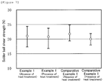
- FIG. 7 is a graph showing solder ball shear strengths of the Ni/Pd/Au films obtained by the electroless plating processes of Example 1 and Comparative Example 1.
- FIG. 8 is a graph showing wire bonding strengths of the Ni/Pd/Au films obtained by the electroless plating processes of Example 1 and Comparative Example 1.
- FIG. 9 is a graph showing gold wire fracture modes of the Ni/Pd/Au films obtained by the electroless plating processes of Example 1 and Comparative Example 1.
- FIG. 10 is a flowchart showing an electroless plating process of a conventional technology.
- the electroless plating process of the present embodiment is an electroless plating process for sequentially forming a nickel film and a gold film on a surface of a copper material of an electrode, a wire and the like which have been provided on a surface of an insulating base material, for example, such as a resin substrate, a ceramic substrate and a wafer substrate, by an electroless plating method.
- the electroless plating process is an electroless plating process including a step of forming the nickel film on the surface of the copper material by an electroless strike plating method, and a step of forming the gold film by a reduction-type electroless plating method.
- an electroless plating process will be described which forms an Ni/Pd/Au film on the surface of the copper material by sequentially forming the nickel film, the palladium film and the gold film on the surface of the copper material.
- a degreasing step (S1), an etching step (S2) and a desmutting step (S3) are carried out as pretreatment before the nickel film is formed.
- the nickel film is formed on the surface of the copper material in an electroless nickel (Ni) strike plating step (S4).
- the palladium film is formed in an electroless palladium (Pd) plating step (S5), and the gold film is formed in an electroless gold (Au) plating step (S6).
- Water washing treatment is performed after each step. It is preferable to perform the water washing treatment three times.
- the copper material is immersed in an acidic solution, and an oil and fat content is removed which adheres to a surface of the copper material.
- the copper material which has been subjected to the degreasing step (S1) is immersed in an etching solution such as a persulfate-based solution, a hydrogen peroxide-based solution, and a thiol-based solution, and a copper oxide film is removed which is formed on a surface of the copper material.
- an etching solution such as a persulfate-based solution, a hydrogen peroxide-based solution, and a thiol-based solution, and a copper oxide film is removed which is formed on a surface of the copper material.
- the copper material which has been subjected to the etching step (S2) is immersed in, for example, 10% sulfuric acid, and a smut is removed which adheres to a surface of the copper material.
- the electroless nickel strike plating step (S4) a nickel film is formed on a surface of the pretreated copper material, by the electroless strike plating method.
- the electroless strike plating method is performed by immersing the copper material which has been subjected to the desmutting step (S3), in an electroless nickel strike plating solution.
- the electroless nickel strike plating solution contains a water-soluble nickel salt, a carboxylic acid or a salt thereof, and one or more reducing agents selected from the group of dimethylamine borane, trimethylamine borane, hydrazine and a hydrazine derivative.
- one or more means that it may be only one, or be two or more.
- water-soluble nickel salts to be used in the electroless nickel strike plating solution examples include nickel sulfate, nickel chloride, nickel carbonate, and nickel salts of organic acids such as nickel acetate, nickel hypophosphite, nickel sulfamate and nickel citrate. These may be used singly or in combinations of two or more. In the present invention, it is most preferable to use the nickel sulfate hexahydrate as the water-soluble nickel salt.
- the content of the water-soluble nickel salt is in a range of 0.002 to 1 g/L in terms of nickel.
- the content within the above range is 1 ⁇ 5 or less of a nickel concentration of 5 g/L in the electroless nickel plating solution which is used in the electroless nickel plating (S15) of the electroless plating process of the conventional technology, and is considerably low concentration.
- the electroless nickel strike plating solution achieves the electroless strike plating method if the content of the water-soluble nickel salt in terms of nickel is within the above described range, and can directly form the nickel film on a surface of a copper material to which a palladium catalyst is not adsorbed.
- the content of the water-soluble nickel salt is less than 0.002 g/L in terms of nickel, because a deposition rate becomes excessively low, and accordingly it becomes necessary to lengthen an immersion time period in order to obtain a nickel film of a desired film thickness, which cannot satisfy the industrial productivity.
- the content of the water-soluble nickel salt exceeds 1 g/L in terms of nickel, because the deposition rate becomes excessively high, and there is a case where a nickel film of which the surface is uniform cannot be obtained. It is more preferable for the content of the water-soluble nickel salt in terms of nickel to be in a range of 0.01 to 0.5 g/L, and is most preferable to be in a range of 0.03 to 0.1 g/L.
- the electroless nickel strike plating solution contains a carboxylic acid or a salt thereof. They act as complexing agents and pH adjusting agents.
- the carboxylic acid one or more can be used which are selected from: monocarboxylic acids (formic acid, acetic acid, propionic acid, butyric acid and the like); dicarboxylic acids (oxalic acid, malonic acid, succinic acid, gluconic acid, adipic acid, fumaric acid, maleic acid, succinic acid and the like); tricarboxylic acids (aconitic acid and the like); hydroxycarboxylic acids (citric acid, lactic acid and malic acid); aromatic carboxylic acids (benzoic acid, phthalic acid, salicylic acid and the like); oxocarboxylic acids (pyruvic acid and the like); and amino acids (arginine, asparagine, aspartic acid, cysteine, glutamic acid, glycine and the like).
- the carboxylic acid or a salt thereof in a range of 0.5 to 5 g/L in total, and is more preferable to use the carboxylic acid or a salt thereof in a range of 0.8 to 2 g/L.
- the nickel content is lower than that of the electroless nickel plating solution which is used in the electroless nickel plating (S15) of the electroless plating process of the conventional technology, and accordingly the content of the carboxylic acid or the salt thereof is set low.
- the content of the carboxylic acid or the salt thereof is less than 0.5 g/L, though depending on the type, because it becomes insufficient for nickel ions in the electroless nickel strike plating solution to form complexes, and precipitation occasionally occurs. On the other hand, it is also not preferable that the content of the carboxylic acid or the salt thereof exceeds 5 g/L, because not only a special effect cannot be obtained but also resources are wasted.
- the electroless nickel strike plating solution contains one or more reducing agents selected from the group of dimethylamine borane, trimethylamine borane, hydrazine and a hydrazine derivative.
- the electroless nickel strike plating solution can achieve the nickel deposition on a surface of a copper material to which the palladium catalyst is not adsorbed, by using these substances as reducing agents. From the viewpoint of safety to the human body, the dimethylamine borane and the trimethylamine borane are more preferable.
- the reducing agent in a range of 2 to 10 g/L, and is more preferable to use the agent in a range of 4 to 8 g/L. It is not preferable that the content of the above described reducing agent is less than 2 g/L, because there is a case where a sufficient reducing action cannot be obtained and the nickel deposition on the copper surface does not progress. It is not preferable that the content of the above described reducing agent exceeds 10 g/L, because there is a case where nickel abnormally deposits on another surface than that of copper (surface of insulating base material), or the decomposition of a bath of the electroless nickel strike plating solution occurs.
- the electroless nickel strike plating solution is prepared by mixing the above described components with water, stirring the mixture and dissolving the components. It is more preferable that the electroless nickel strike plating solution is prepared by mixing and stirring the above described water-soluble nickel salt, the above described carboxylic acid or a salt thereof, and water to prepare an aqueous solution containing a nickel complex, then mixing the above described reducing agent into the aqueous solution, and stirring the mixture.
- the nickel complex can stably exist for a long period of time, and excellent bath stability can be obtained.
- the electroless nickel strike plating solution may contain components such as a sulfate, boric acid and a chloride salt.
- a pH of the electroless nickel strike plating solution is adjusted to a neutral region of 6 to 10. It is not preferable that the pH is lower than 6, because the deposition rate of nickel decreases and the forming property of the nickel film lowers, and pores and non-deposition superfine areas (holes) are occasionally formed on the surface of the nickel film. On the other hand, it is not preferable that the pH exceeds 10, because there are cases where the deposition rate of nickel becomes excessively high, which makes it difficult to control the film thickness of the nickel film, and the crystalline state of depositing nickel cannot be densified.
- the bath temperature of the electroless nickel strike plating solution is adjusted to 20 to 55° C. This is a value lower than the bath temperature of 60 to 90° C. in the electroless nickel plating solution which is used in the electroless nickel plating (S15) of the conventional technology. It is not preferable that the bath temperature is lower than 20° C., because the deposition rate of nickel decreases, the forming property of the nickel film lowers, and there is a case where pores and non-deposition superfine areas (holes) are formed on the surface of the nickel film, or no nickel deposition occurs. On the other hand, it is not preferable that the bath temperature exceeds 55° C., because the bath stability of the electroless nickel strike plating solution decreases, and the electroless strike plating method cannot be occasionally achieved.
- the film thickness of the nickel film is adjusted by the immersion time period in the electroless nickel strike plating solution. It is preferable for the film thickness of the nickel film to be as thin as possible within a range that can prevent copper diffusion, and is preferable to be 0.005 to 0.3 ⁇ m. It is not preferable that the film thickness of the nickel film is less than 0.005 ⁇ m, because it becomes insufficient to cover the surface of the copper material, non-deposition superfine areas are formed on the surface of the nickel film, and as a result, there are cases where the nickel local corrosion phenomenon occurs when the subsequent electroless gold plating step (S6) has been performed, and copper and nickel diffuse into the surface of the gold film. On the other hand, it is possible to form a nickel film of which the film thickness exceeds 0.3 ⁇ m, but is not preferable because the flexibility of the nickel film lowers, and besides, resources are wasted.
- the electroless nickel strike plating step (S4) of the present embodiment it is possible to achieve the thinning of the nickel film, which has been difficult for the conventional electroless nickel plating (S15), and is possible to obtain a nickel film of which the film thickness is 0.005 to 0.3 ⁇ m. Furthermore, in order to achieve the thinning of the film while ensuring favorable mounting characteristics, it is more preferable that the film thickness of the nickel film which is formed in the electroless nickel strike plating step (S4) is 0.007 to 0.1 ⁇ m.
- one or more substances selected from the group of dimethylamine borane, trimethylamine borane, hydrazine and a hydrazine derivative which are contained in the electroless nickel strike plating solution act as reducing agents, and can make nickel deposit on a surface of the copper material to which the palladium catalyst is not adsorbed.
- the nickel content of the electroless nickel strike plating solution is low; and besides, the pH is adjusted to 6 to 10, and the bath temperature is adjusted to 20 to 55° C. Thereby, the deposition rate of nickel can be lowered, the electroless strike plating method can be achieved, and the nickel film can be directly formed on the surface of the copper material.
- the deposition rate of nickel is low, accordingly it is possible to uniformly deposit nickel on the surface of the copper material, and as a result, it is possible to form a nickel film which is uniform in film thickness, and surely covers the surface of the copper material even though the film thickness is thin.
- the obtained nickel film is excellent in adhesiveness to the copper material and excellent in barrier properties, i.e., prevention of the diffusion of copper, as compared with the nickel film which has been obtained in the conventional electroless plating process.
- the palladium which has been adsorbed on the surface of the copper material by the palladium catalyst adsorption treatment (S14) acts as a catalyst, and the nickel deposition progresses. Because of this, variations of the film thicknesses of the nickel film to be formed occur between a region in which the palladium catalyst has been adsorbed and a region in which the palladium catalyst has not been adsorbed, on the surface of the copper material, and it is difficult to obtain the nickel film of which the film thickness is uniform.
- the nickel content and the bath temperature are high, accordingly the deposition rate of nickel is high, and accordingly it is difficult to obtain the nickel film excellent in the adhesiveness to the copper material.
- the electroless nickel strike plating step (S4) of the present embodiment when the dimethylamine borane or the trimethylamine borane is used as a reducing agent, it is possible to obtain a nickel film formed from an alloy of nickel and boron (nickel-boron alloy). This nickel film contains a very small amount of boron (for example, 0.1% or less), and is a nickel film which is substantially formed of pure nickel.
- the hydrazine or the hydrazine derivative is used as a reducing agent, it is possible to obtain a nickel film formed of pure nickel.
- the content of the water-soluble nickel salt in the above described electroless nickel strike plating solution is as low as 0.002 to 1 g/L. Because of this, it is possible to prevent the bath decomposition from occurring even without using a stabilizer such as a lead salt or bismuth salt which is used in the electroless nickel plating (S15) of the electroless plating process of the conventional technology.
- the above described electroless nickel strike plating solution does not contain the stabilizer such as the lead salt and the bismuth salt, and accordingly it is possible to obtain a nickel film which does not contain a heavy metal such as lead and bismuth.
- a palladium film is formed on the surface of the above described nickel film by a reduction-type electroless plating method.
- a palladium film is formed by a substitution-type electroless plating method, there is a case where a nickel local corrosion phenomenon occurs, specifically, a phenomenon in which nickel dissolves and a through hole penetrating the nickel film is formed occurs; and accordingly the reduction-type electroless plating method is adopted.
- the reduction-type electroless palladium plating solution which is used in the electroless palladium plating step (S5) a known plating solution can be used.
- a reduction-type electroless palladium plating solution which contains 0.001 to 0.1 mol/L of a palladium compound, 0.05 to 5 mol/L of an amine compound, 0.01 to 0.1 mol/L of an inorganic sulfur compound, and 0.05 to 1.0 mol/L of hypophosphorous acid or a hypophosphorous acid compound.
- the reduction-type electroless plating method is adopted, and thereby it becomes possible to prevent the dissolution of nickel from the nickel film when forming the palladium film.
- the nickel film which has been formed by the electroless nickel strike plating step (S4) is uniform in film thickness and is excellent in smoothness, and accordingly it is possible to form a palladium film having a uniform film thickness, according to the electroless palladium plating step (S5).
- the electroless gold plating step (S6) a gold film is formed on the surface of the above described palladium film by a reduction-type electroless plating method.
- the gold film is formed by the substitution-type electroless plating method, there is a case where palladium dissolves and a through hole is formed in the palladium film; and accordingly the reduction-type electroless plating method is adopted.
- the reduction-type electroless gold plating solution which is used in the electroless gold plating step (S6) a known plating solution can be used.
- a reduction-type electroless gold plating solution that contains: a water-soluble gold compound; citric acid or a salt thereof; ethylenediaminetetraacetic acid or a salt thereof; hexamethylenetetramine as a reducing agent; and chain polyamine which contains an alkyl group having 3 or more carbon atoms, and 3 or more amino groups.
- the reduction-type electroless plating method is adopted, and thereby it becomes possible to prevent the dissolution of palladium from the palladium film when forming the gold film.
- the palladium plating which has been formed by the electroless palladium plating step (S4) has a uniform film thickness, and accordingly it is possible to form a gold film having a uniform film thickness, according to the electroless gold plating step (S6).
- the electroless plating process of the present embodiment it is possible to form the nickel film directly on the surface of the copper material to which the palladium catalyst is not adsorbed, by the electroless nickel strike plating step (S4).
- the nickel film which surely covers the surface of the copper material even though the film thickness is thin, and is excellent in the adhesiveness to the copper material and the barrier properties. Accordingly, it is possible to achieve the thinning of the nickel film.
- the nickel film Furthermore, it is possible to thin the film thickness of the nickel film, and accordingly it is possible to obtain an Ni/Pd/Au film of which the overall film thickness is thin.
- the nickel film which has been formed by the electroless strike plating method is excellent in the adhesiveness to the copper material and excellent in the barrier properties of preventing the diffusion of copper, and accordingly it is possible to form the Ni/Pd/Au film having excellent mounting characteristics.
- the above described nickel film has a thin film thickness, and besides, does not contain phosphor unlike the nickel film which is formed by the electroless nickel plating (S15) of the conventional technology. From this result, the above described nickel film can obtain excellent flexibility, and accordingly the Ni/Pd/Au film can obtain the excellent flexibility.
- the electroless plating process of the present embodiment unlike the electroless plating process of the conventional technology, there is no need to perform the palladium catalyst adsorption treatment (S14) before the electroless nickel strike plating step (S4), and it is possible to reduce the number of steps.
- the above described electroless plating process of the present embodiment is a process for performing the electroless palladium plating step (S5) and the electroless gold plating step (S6) after the electroless nickel strike plating step (S4).
- the electroless plating process of the present embodiment may be a process for performing the electroless gold plating step (S6) without performing the electroless palladium plating step (S5), after the electroless nickel strike plating step (S4), and thereby forming an Ni/Au film on the surface of the copper material.
- an Ni/Pd/Au film was formed on a surface of a copper material by sequentially performing each step of S1 to S6 (6 steps in all) shown in FIG. 1 .
- the electroless nickel strike plating step (S4) was performed.
- the copper material was immersed in an electroless nickel strike plating solution having the following composition, and a nickel film was formed on the surface of the copper material.
- the electroless nickel strike plating solution was prepared by mixing and stirring nickel sulfate hexahydrate, DL-malic acid and water to prepare an aqueous solution containing a nickel complex, then adding dimethylamine borane, and stirring the mixture. While the copper material was immersed in the electroless nickel strike plating solution, the electroless nickel strike plating solution was stirred by aeration.
- an electroless palladium plating step (S5) was performed.
- a copper material on which the nickel film was formed was immersed in a reduction-type electroless palladium plating solution having the following composition, and a palladium film was formed on the surface of the nickel film.
- an electroless gold plating step (S6) was performed.
- a copper material on which the palladium film was formed was immersed in a reduction-type electroless gold plating solution having the following composition, and a gold film was formed on the surface of the palladium film.
- the Ni/Pd/Au film was formed on the surface of the copper material.
- an Ni/Pd/Au film was formed on a surface of a copper material in exactly the same way as that of the electroless plating process of Example 1, except that in place of the electroless nickel strike plating step (S4), the palladium catalyst adsorption treatment (S14) and the electroless nickel plating (S15) were performed which are performed in the electroless plating process of a conventional technology.
- the steps of the electroless plating process of the present comparative example were 7 steps in all.
- a desmutted copper material was immersed in a palladium catalyst solution containing a palladium compound in a concentration of 30 mg/L in terms of palladium and sulfate ions, and a palladium catalyst was absorbed on the surface of the copper material.
- An electroless plating process of the present comparative example was performed in exactly the same way as that of Comparative Example 1, except that an electroless nickel plating solution having the following composition was used in the electroless nickel plating (S15).
- the steps of the electroless plating process of the present comparative example were 7 steps in all.
- An electroless plating process of the present reference example was performed in exactly the same way as that of the Comparative Example 1, except that the palladium catalyst adsorption treatment (S14) was not performed before the electroless nickel plating (S15) was performed.
- the steps of the electroless plating process of the present reference example were 6 steps in all.
- An electroless plating process of the present reference example was performed in exactly the same way as that of the Comparative Example 2, except that the palladium catalyst adsorption treatment (S14) was not performed before the electroless nickel plating (S15) was performed.
- a nickel film of which the film thickness is 0.01 ⁇ m was formed on a surface of a copper material, by performing the steps up to the electroless nickel strike plating step (S4) in the electroless plating process of Example 1, or by performing the steps up to the electroless nickel plating (S15) in the electroless plating processes of Comparative Example 1 and Comparative Example 2.
- the obtained nickel film was subjected to the following evaluations.
- a test board was used in which 30 copper pads of which the diameter is 0.45 mm are arranged on an insulating base material in a lattice pattern at spaces of 30 ⁇ m. Then, a nickel film was formed on the surface of the copper pad, by performing the steps up to the electroless nickel strike plating step (S4) in the electroless plating process of Example 1, or by performing the steps up to the electroless nickel plating (S15) in the electroless plating processes of Comparative Example 1 and Comparative Example 2. On the other hand, in the electroless plating processes of Reference Example 1 and Reference Example 2, the steps up to the electroless nickel plating (S15) were performed, but nickel was not deposited at all on the surface of the copper pad, and the nickel film could not be formed.
- the obtained nickel film was observed with a metallurgical microscope (magnification of 1000 times), and the number of copper pads was counted on which nickel was normally deposited.
- “the nickel was normally deposited” means that the whole surface of the copper pad is covered with the nickel film, and the uncovered part is not confirmed with the metallurgical microscope.
- the results are shown in Table 1.
- the determination criteria of ⁇ , ⁇ and X in Table 1 are as follows.
- Copper pads on which nickel is normally deposited are 30 pads.
- Copper pads on which nickel is normally deposited are 15 to 29 pads.
- the electroless nickel plating (S15) of Comparative Example 1 can always normally deposit nickel, but the electroless nickel plating (S15) of Comparative Example 2 sometimes fails to normally deposit nickel, and is inferior in a nickel deposition property.
- the electroless nickel strike plating step (S4) of Example 1 can normally deposit nickel and is excellent in the nickel deposition property.
- FIGS. 2 to 4 show a COMPO image of the nickel film which was obtained by the electroless nickel strike plating step (S4) of Example 1;
- FIG. 3 shows a COMPO image of the nickel film which was obtained by the electroless nickel plating (S15) of Comparative Example 1;
- FIG. 4 shows a COMPO image of the nickel film which was obtained by the electroless nickel plating (S15) of Comparative Example 2.
- Magnifications of FIGS. 2( a ), 3( a ) and 4( a ) are 5000 times, and magnifications of FIG. 2( b ) , FIG. 3( b ) and FIG. 4 ( b ) are 30000 times.
- the nickel film can be obtained which is dense and is excellent in the smoothness, according to the electroless nickel strike plating step (S4) of the electroless plating process of Example 1, as compared to the electroless nickel plating (S15) of the electroless plating process of Comparative Example 1 and Comparative Example 2.
- the nickel film which was formed on the surface of the copper pad was subjected to a surface elemental analysis by an Auger Electron Spectroscopy Analyzer. As described above, the nickel film of Comparative Example 2 is inferior in the performance, and accordingly only the nickel film of Example 1 and Comparative Example 1 were targeted.
- the nickel film was subjected to reflow treatment three times.
- the reflow treatment was performed by preliminarily heating the nickel film at 230° C., and then heating the resultant film at 250° C.
- the surface elemental analysis was performed before the nickel film was subjected to the reflow treatment and after the nickel film was subjected to the reflow treatment and then was naturally cooled to normal temperature.
- an acceleration voltage was set at 10 kV
- a probe current value was set at 10 nA
- a measuring diameter was set at 50 ⁇ m
- a scanning range was set at 30 to 2400 eV.
- Table 2 The numerical values in Table 2 are values which have been obtained by quantifying the elements from the peak intensity ratio of the obtained spectrum (unit: atomic %).
- the mark - in Table 2 means that the corresponding element has not been detected at all.
- the nickel film obtained by the electroless nickel strike plating step (S4) of Example 1 contained boron which originated in dimethylamine borane, but in fact, boron was not detected, and it was found that the nickel film was formed from substantially pure nickel.
- the nickel film obtained by the electroless nickel plating (S15) of Comparative Example 1 was formed from a nickel-phosphorus alloy containing phosphorus which originated in sodium hypophosphite.
- a copper plate was used in place of the above described test board, and a nickel film of which the film thickness was 0.01 ⁇ m was formed on the surface of the copper plate. Then, the obtained nickel film was subjected to a low potential electrolysis of 50 mV in a 0.5% by volume of a sulfuric acid solution, and barrier properties were evaluated. The results are shown in FIG. 5 .
- the horizontal axis is an electrolysis time period, and the vertical axis is a current density. The increase in the current density indicates that copper has dissolved from the copper material which is a lower layer of the nickel film.
- the nickel film obtained by the electroless nickel strike plating step (S4) of Example 1 shows a small increase in the current density, as compared to the nickel film obtained by the electroless nickel plating (S15) of Comparative Example 1, and accordingly is excellent in the barrier properties.
- the electroless nickel strike plating step (S4) of the electroless plating process of Example 1 can obtain the nickel film which is excellent in the nickel deposition property, is dense and smooth, and is excellent in the barrier performance, as compared to the electroless nickel plating (S15) of the electroless plating processes of Comparative Example 1 and Comparative Example 2.
- the nickel film obtained by the electroless nickel strike plating step (S4) in the electroless plating process of Example 1 has a superior performance to a nickel film which has the same film thickness as the above film and has been obtained by the electroless nickel plating (S15) of the electroless plating processes of Comparative Example 1 and Comparative Example 2.
- a test board was used in which fine wires of copper of which the wiring width/wiring space (L/S) was 30 to 100 ⁇ m/30 to 100 ⁇ m were arranged on an insulating base material, and also copper pads of which fine wires had a diameter of 0.45 mm were arranged in a lattice form at spaces of 0.45 ⁇ m.
- This test board was subjected to all 6 steps of the electroless plating process of Example 1, or to all seven steps of the electroless plating process of Comparative Example 1, and thereby an Ni/Pd/Au film was formed on the surface of the copper material (fine wires and pads).
- the Ni/Pd/Au film was obtained that was formed of the nickel film of which the film thickness was 0.01 ⁇ m, the palladium film of which the film thickness was 0.1 ⁇ m, and the gold film of which the film thickness was 0.1 ⁇ m.
- the Ni/Pd/Au film was obtained that was formed of the nickel film of which the film thickness was 0.5 ⁇ m, the palladium film of which the film thickness was 0.1 ⁇ m, and the gold film of which the film thickness was 0.1 ⁇ m. Then, the obtained Ni/Pd/Au films were subjected to the following evaluation.
- the surface of the Ni/Pd/Au film was soldered, and then the solder spread test was performed.
- Eco Solder (registered trademark) M770 made by SENJU METAL INDUSTRY CO., LTD. was used as a solder ball, and the diameter D of the solder ball was set at 700 ⁇ m.
- the solder spread test was performed by using a solder reflow furnace (Japan Pulse Laboratories, Inc., RF-330), at a preheating temperature of 230° C. and a reflow temperature of 250° C., with the use of AGF-780DS-AA made by Asahi Chemical Research Laboratory Co., Ltd. as a flux.
- the height H ( ⁇ m) of the solder ball was measured after the reflow; and the spreading rate S was calculated according to the following expression, and the maximum value, the minimum value and the average value thereof were determined. Furthermore, the Ni/Pd/Au film which was subjected to heat treatment at 250° C. for 4 hours before soldering was also subjected to the solder spread test similarly. The results are shown in FIG. 6 . “Absence of heat treatment” in FIG.
- Example 6 shows results of the solder spread test of the Ni/Pd/Au film which was soldered without being subjected to the above described heat treatment after the electroless plating process of Example 1 or Comparative Example 1, and “presence of heat treatment” shows results of the Ni/Pd/Au film which was soldered after having been subjected to the above described electroless plating process and subsequently to the above described heat treatment.
- the Ni/Pd/Au film obtained by the electroless plating process of Example 1 is excellent in solder spreadability, in both of the absence of heat treatment and the presence of heat treatment, as compared with the Ni/Pd/Au film obtained by the electroless plating process of Comparative Example 1.
- the absence of heat treatment is compared with the presence of heat treatment, in the Ni/Pd/Au film obtained by the electroless plating process of Example 1, differences between average values and minimum values are small, but on the other hand, in the Ni/Pd/Au film obtained by the electroless plating process of Comparative Example 1, the average value greatly decreases.
- the Ni/Pd/Au film obtained by the electroless plating process of Example 1 shows a high effect of suppressing the diffusion of copper or nickel into the gold film by heat treatment, and can maintain excellent solder spreadability even when the heat treatment has been performed, and has excellent heat resistance.
- the surface of the Ni/Pd/Au film was soldered, and then a solder ball shear strength was measured.
- the solder ball shear strength was measured at a shear height of 20 ⁇ m and a shear rate of 500 ⁇ m/sec with the use of a solder ball shear tester made by Nordson Dage (Series 4000), and the maximum value, the minimum value and the average value thereof were determined.
- the solder ball shear strength was similarly measured for the Ni/Pd/Au film which was subjected to heat treatment of 250° C. for 4 hours before soldering. The results are shown in FIG. 7 . “Absence of heat treatment” in FIG.
- Example 7 shows a solder ball shear strength of the Ni/Pd/Au film which has been soldered without being subjected to the above described heat treatment after the electroless plating process of Example 1 or Comparative Example 1, and “presence of heat treatment” shows a result of the Ni/Pd/Au film which has been soldered after having been subjected to the above described heat treatment following the above described electroless plating process.
- the Ni/Pd/Au film obtained by the electroless plating process of Example 1 has an excellent solder ball shear strength though the numerical value itself is low, in both of the absence of heat treatment and the presence of heat treatment, as compared with the Ni/Pd/Au film obtained by the electroless plating process of Comparative Example 1.
- the absence of heat treatment is compared with the presence of heat treatment
- differences between average values and minimum values are small, but on the other hand, in the Ni/Pd/Au film obtained by the electroless plating process of Comparative Example 1, the average value and the minimum value after the heat treatment greatly decrease from those before the heat treatment.
- the Ni/Pd/Au film obtained by the electroless plating process of Example 1 shows a high effect of suppressing the diffusion of copper or nickel into the gold film by heat treatment, can maintain an excellent solder ball shear strength even when the heat treatment has been performed, and has excellent heat resistance, as compared to the Ni/Pd/Au film obtained by the electroless plating process of Comparative Example 1.
- the Ni/Pd/Au film obtained by the electroless plating process of Example 1 has the wire bonding strength of the same level as that of the Ni/Pd/Au film which was obtained by the electroless plating process of Comparative Example 1 and was not subjected to heat treatment, in both of the absence of heat treatment and the presence of heat treatment.
- the absence of heat treatment is compared with the presence of heat treatment, in the Ni/Pd/Au film obtained by the electroless plating process of Example 1, differences between average values and minimum values are small, but on the other hand, in the Ni/Pd/Au film obtained by the electroless plating process of Comparative Example 1, the average value and the minimum value greatly decrease.
- the fracture modes when the gold wire was fractured were all C modes, in both of the absence of heat treatment and the presence of heat treatment.
- the Ni/Pd/Au film obtained by the electroless plating process of Comparative Example 1 in the absence of heat treatment, all are the C mode, and in the presence of the heat treatment, 45% were the C mode and 55% were an E mode.
- the Ni/Pd/Au film obtained by the electroless plating process of Example 1 shows a high effect of suppressing the diffusion of copper or nickel into the gold film by heat treatment, can maintain a wire bonding strength and the fracture mode even when the heat treatment has been performed, and has excellent heat resistance, as compared to the Ni/Pd/Au film obtained by the electroless plating process of Comparative Example 1.
- the Ni/Pd/Au film obtained by the electroless plating process of Example 1 has excellent mounting characteristics which are equal to or better than that of the Ni/Pd/Au film obtained by the electroless plating process of Comparative Example 1, though the film thickness of the nickel film is 1/50. This is considered to be because the nickel film which is formed in the electroless nickel strike plating step (S4) of the electroless plating process of Example 1 is dense and smooth, and is excellent in the barrier performance.
- the electroless plating process of the present invention it is possible to form an Ni/Au film or an Ni/Pd/Au film on a surface of a copper material.
- the obtained nickel film can surely cover the surface of the copper material even though the film thickness is thin, and accordingly it is possible to achieve the thinning of the nickel film according to the electroless plating process of the present invention.
- the electroless plating process of the present invention can cope with a complicated wiring pattern and wiring with narrow pitches, and can achieve high density mounting of electronic parts.
- the obtained Ni/Au film or Ni/Pd/Au film has a thin overall film thickness and is excellent in flexibility; and accordingly is suitable as a flexible substrate.
- the electroless plating process according to the present invention can form the nickel film even without performing the palladium catalyst adsorption treatment (S14) which has been performed in a conventional electroless plating process, and accordingly can improve the productivity.
Abstract
Description
- The present invention relates to an electroless plating process for forming a gold film on a surface of a copper material by an electroless plating method.
- In recent years, demands have been increasing for a higher function and more multiple function of electronic equipment, but electronic circuit boards such as a resin substrate, a ceramic substrate and a wafer substrate, which are used in these electronic equipment, are required to become further lighter, thinner, shorter and smaller. In order to cope with this tendency of being lighter, thinner, shorter and smaller, high density mounting of electronic parts is necessary, and accordingly a surface treatment technology is required which can achieve the high density mounting. In addition, in a technological field of electronic circuit boards, a mounting technology using solder or wire bonding has been established as a technology for bonding mounted components.
- For the purpose of ensuring the connection reliability at the time of mounting, plating treatment is performed as surface treatment, on a wiring pad which is a mounting portion of a circuit pattern on an electronic circuit board. For example, a nickel film and a gold film are sequentially formed by plating treatment, on a circuit pattern which is formed of a low resistance metal such as copper. Hereinafter, a film formed of the nickel film and the gold film which have been sequentially formed will be described as “Ni/Au film”. The nickel film is formed so as to prevent the diffusion of copper into the gold film, and the gold film is formed so as to obtain adequate mounting characteristics.
- Furthermore, a technology of forming a palladium film between a nickel film and a gold film is also known. Hereinafter, a film formed of the nickel film, the palladium film and the gold film which have been sequentially formed will be described as “Ni/Pd/Au film”. The palladium film is formed in order to prevent nickel from diffusing into the gold film when the plated substrate is heat treated. When the palladium film has been formed on the nickel film, it becomes possible to thin the nickel film.
- As the above described plating treatment, an electrolytic plating process is the mainstream, but an electroless plating process is applied to those which the electrolytic plating process cannot cope with.
- As for a conventional electroless plating process for forming an Ni/Pd/Au film on the surface of copper, for example, such a process is disclosed in
Patent Literature 1 for performing a degreasing step (step (hereinafter referred to as “S”) 11) and etching (S12) onto a copper material, as shown inFIG. 10 , adsorbing a palladium catalyst to a surface of the copper material (S14), and then performing electroless nickel (Ni) plating (S15), electroless palladium (Pd) plating (S16) and electroless gold (Au) plating (S17). Although not described inPatent Literature 1, it is general to perform desmut (S13) between etching (S12) and palladium catalyst adsorption treatment (S14). The palladium catalyst adsorption treatment (S14) is usually essential for progressing nickel deposition at the time of electroless nickel plating (S15). - In the electroless nickel plating (S15) disclosed in
Patent Literature 1, an electroless nickel plating solution is used which contains nickel sulfate hexahydrate in a concentration of 22.5 g/L (5 g/L in terms of nickel), sodium hypophosphite as a reducing agent, malic acid and succinic acid as complexing agents, also contains a lead salt, a bismuth salt, a sulfur compound or the like as stabilizers, and has a pH adjusted to 4.6 and a bath temperature adjusted to 60 to 90° C. It is also possible to use dimethylamine borane in place of sodium hypophosphite, as the reducing agent. Then, it is described that a nickel film of which the film thickness is 0.1 to 15 μm is formed by the electroless nickel plating (S15), a palladium film of which the film thickness is 0.001 to 2 μm is formed by electroless palladium plating (S16), and a gold film of which the film thickness is 0.001 to 1 μm is formed by electroless gold plating (S17). - In order to achieve further high density mounting of electronic parts in the Ni/Au film or the Ni/Pd/Au film, it is desired to further thin the nickel film.
- [Patent Literature 1] Japanese Patent Laid-Open No. 2008-174774
- However, when an extremely thin nickel film of which the film thickness is, for example, 0.01 μm or less is formed by the above described electroless nickel plating (S15), there is a case where the covering becomes insufficient and a non-deposition superfine area (hole) is formed on the surface of the nickel film. Then, when the subsequent electroless gold plating (S17) has been performed, there is a case where the non-deposition superfine area is corroded and a through hole is formed which penetrates through the nickel film. This phenomenon is referred to as “nickel local corrosion phenomenon”. In that case, there is a disadvantage in the Ni/Au film or the Ni/Pd/Au film that excellent mounting characteristics cannot be obtained.
- An object of the present invention is to provide an electroless plating process which can thin a film thickness of a nickel film and can obtain a film having excellent mounting characteristics, when the nickel film and the gold film are sequentially formed on a surface of a copper material.
- The electroless plating process according to the present invention is an electroless plating process for sequentially forming a nickel film and a gold film on a surface of a copper material by an electroless plating method, and includes: a step of forming the nickel film on the surface of the copper material by an electroless strike plating method; and a step of forming the gold film by a reduction-type electroless plating method.
- In the electroless plating process according to the present invention, it is preferable to perform the electroless strike plating method by using an electroless nickel strike plating solution that contains a water-soluble nickel salt in a concentration of 0.002 to 1 g/L in terms of nickel, a carboxylic acid or a salt thereof, and one or more reducing agents selected from the group of dimethylamine borane, trimethylamine borane, hydrazine and a hydrazine derivative, and has a pH adjusted to 6 to 10 and a bath temperature adjusted to 20 to 55° C., and immersing the copper material in the electroless nickel strike plating solution.
- In addition, it is preferable that the electroless nickel strike plating solution is prepared by mixing and stirring the water-soluble nickel salt, the carboxylic acid or the salt thereof and water to prepare an aqueous solution containing a nickel complex, then mixing the reducing agent into the aqueous solution, and stirring the mixture.
- In the electroless plating process according to the present invention, it is preferable that the step of forming the nickel film is a step of forming a nickel film of which the film thickness is 0.005 to 0.3 μm.
- Furthermore, it is preferable that the electroless plating process according to the present invention is a process for sequentially forming a nickel film, a palladium film and a gold film on a surface of a copper material, and includes a step of forming a palladium film by a reduction-type electroless plating method between the step of forming the nickel film and the step of forming the gold film.
- The electroless plating process according to the present invention adopts the electroless strike plating method, and thereby can directly form the nickel film on the surface of the copper material even without performing the palladium catalyst adsorption treatment (S14) which has been performed in a conventional electroless plating process. In addition, it is possible to form a nickel film which surely covers the surface of the copper material even though the film thickness is thin, and is excellent in adhesiveness to the copper material. Because of this, according to the electroless plating process of the present invention, it is possible to achieve the thinning of the nickel film. In addition, the electroless plating process according to the present invention adopts the reduction-type electroless plating method, and thereby can form the gold film or the palladium film without dissolving a metal of the film which has been precedingly formed. According to the electroless plating process of the present invention, it is possible to obtain an Ni/Au film or Ni/Pd/Au film which is excellent in mounting characteristics.
-
FIG. 1 is a flowchart showing an electroless plating process of the present embodiment. -
FIG. 2 is an SEM photograph of a nickel film obtained by an electroless plating process of Example 1. -
FIG. 3 is an SEM photograph of a nickel film obtained by an electroless plating process of Comparative Example 1. -
FIG. 4 is an SEM photograph of a nickel film obtained by an electroless plating process of Comparative Example 2. -
FIG. 5 is a graph showing results of having electrolyzed the nickel films obtained by the electroless plating processes of Example 1 and Comparative Example 1, at a low potential. -
FIG. 6 is a graph showing solder spreadabilities of Ni/Pd/Au films obtained by the electroless plating processes of Example 1 and Comparative Example 1. -
FIG. 7 is a graph showing solder ball shear strengths of the Ni/Pd/Au films obtained by the electroless plating processes of Example 1 and Comparative Example 1. -
FIG. 8 is a graph showing wire bonding strengths of the Ni/Pd/Au films obtained by the electroless plating processes of Example 1 and Comparative Example 1. -
FIG. 9 is a graph showing gold wire fracture modes of the Ni/Pd/Au films obtained by the electroless plating processes of Example 1 and Comparative Example 1. -
FIG. 10 is a flowchart showing an electroless plating process of a conventional technology. - Next, an embodiment of the electroless plating process according to the present invention will be described. The electroless plating process of the present embodiment is an electroless plating process for sequentially forming a nickel film and a gold film on a surface of a copper material of an electrode, a wire and the like which have been provided on a surface of an insulating base material, for example, such as a resin substrate, a ceramic substrate and a wafer substrate, by an electroless plating method. Specifically, the electroless plating process is an electroless plating process including a step of forming the nickel film on the surface of the copper material by an electroless strike plating method, and a step of forming the gold film by a reduction-type electroless plating method. Hereinafter, an electroless plating process will be described which forms an Ni/Pd/Au film on the surface of the copper material by sequentially forming the nickel film, the palladium film and the gold film on the surface of the copper material.
- In the electroless plating process of the present embodiment, firstly, as shown in
FIG. 1 , a degreasing step (S1), an etching step (S2) and a desmutting step (S3) are carried out as pretreatment before the nickel film is formed. After that, the nickel film is formed on the surface of the copper material in an electroless nickel (Ni) strike plating step (S4). Subsequently, the palladium film is formed in an electroless palladium (Pd) plating step (S5), and the gold film is formed in an electroless gold (Au) plating step (S6). Water washing treatment is performed after each step. It is preferable to perform the water washing treatment three times. - In the degreasing step (S1), the copper material is immersed in an acidic solution, and an oil and fat content is removed which adheres to a surface of the copper material.
- In the etching step (S2), the copper material which has been subjected to the degreasing step (S1) is immersed in an etching solution such as a persulfate-based solution, a hydrogen peroxide-based solution, and a thiol-based solution, and a copper oxide film is removed which is formed on a surface of the copper material.
- In the desmutting step (S3), the copper material which has been subjected to the etching step (S2) is immersed in, for example, 10% sulfuric acid, and a smut is removed which adheres to a surface of the copper material.
- In the electroless nickel strike plating step (S4), a nickel film is formed on a surface of the pretreated copper material, by the electroless strike plating method. The electroless strike plating method is performed by immersing the copper material which has been subjected to the desmutting step (S3), in an electroless nickel strike plating solution.
- The electroless nickel strike plating solution contains a water-soluble nickel salt, a carboxylic acid or a salt thereof, and one or more reducing agents selected from the group of dimethylamine borane, trimethylamine borane, hydrazine and a hydrazine derivative. In the present specification, “one or more” means that it may be only one, or be two or more.
- Examples of the water-soluble nickel salts to be used in the electroless nickel strike plating solution include nickel sulfate, nickel chloride, nickel carbonate, and nickel salts of organic acids such as nickel acetate, nickel hypophosphite, nickel sulfamate and nickel citrate. These may be used singly or in combinations of two or more. In the present invention, it is most preferable to use the nickel sulfate hexahydrate as the water-soluble nickel salt.
- As for the electroless nickel strike plating solution, it is preferable that the content of the water-soluble nickel salt is in a range of 0.002 to 1 g/L in terms of nickel. The content within the above range is ⅕ or less of a nickel concentration of 5 g/L in the electroless nickel plating solution which is used in the electroless nickel plating (S15) of the electroless plating process of the conventional technology, and is considerably low concentration. The electroless nickel strike plating solution achieves the electroless strike plating method if the content of the water-soluble nickel salt in terms of nickel is within the above described range, and can directly form the nickel film on a surface of a copper material to which a palladium catalyst is not adsorbed.
- It is not preferable that the content of the water-soluble nickel salt is less than 0.002 g/L in terms of nickel, because a deposition rate becomes excessively low, and accordingly it becomes necessary to lengthen an immersion time period in order to obtain a nickel film of a desired film thickness, which cannot satisfy the industrial productivity. On the other hand, it is not preferable that the content of the water-soluble nickel salt exceeds 1 g/L in terms of nickel, because the deposition rate becomes excessively high, and there is a case where a nickel film of which the surface is uniform cannot be obtained. It is more preferable for the content of the water-soluble nickel salt in terms of nickel to be in a range of 0.01 to 0.5 g/L, and is most preferable to be in a range of 0.03 to 0.1 g/L.
- The electroless nickel strike plating solution contains a carboxylic acid or a salt thereof. They act as complexing agents and pH adjusting agents. As the carboxylic acid, one or more can be used which are selected from: monocarboxylic acids (formic acid, acetic acid, propionic acid, butyric acid and the like); dicarboxylic acids (oxalic acid, malonic acid, succinic acid, gluconic acid, adipic acid, fumaric acid, maleic acid, succinic acid and the like); tricarboxylic acids (aconitic acid and the like); hydroxycarboxylic acids (citric acid, lactic acid and malic acid); aromatic carboxylic acids (benzoic acid, phthalic acid, salicylic acid and the like); oxocarboxylic acids (pyruvic acid and the like); and amino acids (arginine, asparagine, aspartic acid, cysteine, glutamic acid, glycine and the like).
- It is preferable to use the carboxylic acid or a salt thereof in a range of 0.5 to 5 g/L in total, and is more preferable to use the carboxylic acid or a salt thereof in a range of 0.8 to 2 g/L. In the electroless nickel strike plating solution of the present embodiment, the nickel content is lower than that of the electroless nickel plating solution which is used in the electroless nickel plating (S15) of the electroless plating process of the conventional technology, and accordingly the content of the carboxylic acid or the salt thereof is set low. It is not preferable that the content of the carboxylic acid or the salt thereof is less than 0.5 g/L, though depending on the type, because it becomes insufficient for nickel ions in the electroless nickel strike plating solution to form complexes, and precipitation occasionally occurs. On the other hand, it is also not preferable that the content of the carboxylic acid or the salt thereof exceeds 5 g/L, because not only a special effect cannot be obtained but also resources are wasted.
- The electroless nickel strike plating solution contains one or more reducing agents selected from the group of dimethylamine borane, trimethylamine borane, hydrazine and a hydrazine derivative. The electroless nickel strike plating solution can achieve the nickel deposition on a surface of a copper material to which the palladium catalyst is not adsorbed, by using these substances as reducing agents. From the viewpoint of safety to the human body, the dimethylamine borane and the trimethylamine borane are more preferable.
- It is preferable to use the reducing agent in a range of 2 to 10 g/L, and is more preferable to use the agent in a range of 4 to 8 g/L. It is not preferable that the content of the above described reducing agent is less than 2 g/L, because there is a case where a sufficient reducing action cannot be obtained and the nickel deposition on the copper surface does not progress. It is not preferable that the content of the above described reducing agent exceeds 10 g/L, because there is a case where nickel abnormally deposits on another surface than that of copper (surface of insulating base material), or the decomposition of a bath of the electroless nickel strike plating solution occurs.
- The electroless nickel strike plating solution is prepared by mixing the above described components with water, stirring the mixture and dissolving the components. It is more preferable that the electroless nickel strike plating solution is prepared by mixing and stirring the above described water-soluble nickel salt, the above described carboxylic acid or a salt thereof, and water to prepare an aqueous solution containing a nickel complex, then mixing the above described reducing agent into the aqueous solution, and stirring the mixture. In the electroless nickel strike plating solution thus prepared, the nickel complex can stably exist for a long period of time, and excellent bath stability can be obtained.
- Besides the above described components, the electroless nickel strike plating solution may contain components such as a sulfate, boric acid and a chloride salt.
- pH:
- It is preferable that a pH of the electroless nickel strike plating solution is adjusted to a neutral region of 6 to 10. It is not preferable that the pH is lower than 6, because the deposition rate of nickel decreases and the forming property of the nickel film lowers, and pores and non-deposition superfine areas (holes) are occasionally formed on the surface of the nickel film. On the other hand, it is not preferable that the pH exceeds 10, because there are cases where the deposition rate of nickel becomes excessively high, which makes it difficult to control the film thickness of the nickel film, and the crystalline state of depositing nickel cannot be densified.
- It is preferable that the bath temperature of the electroless nickel strike plating solution is adjusted to 20 to 55° C. This is a value lower than the bath temperature of 60 to 90° C. in the electroless nickel plating solution which is used in the electroless nickel plating (S15) of the conventional technology. It is not preferable that the bath temperature is lower than 20° C., because the deposition rate of nickel decreases, the forming property of the nickel film lowers, and there is a case where pores and non-deposition superfine areas (holes) are formed on the surface of the nickel film, or no nickel deposition occurs. On the other hand, it is not preferable that the bath temperature exceeds 55° C., because the bath stability of the electroless nickel strike plating solution decreases, and the electroless strike plating method cannot be occasionally achieved.
- The film thickness of the nickel film is adjusted by the immersion time period in the electroless nickel strike plating solution. It is preferable for the film thickness of the nickel film to be as thin as possible within a range that can prevent copper diffusion, and is preferable to be 0.005 to 0.3 μm. It is not preferable that the film thickness of the nickel film is less than 0.005 μm, because it becomes insufficient to cover the surface of the copper material, non-deposition superfine areas are formed on the surface of the nickel film, and as a result, there are cases where the nickel local corrosion phenomenon occurs when the subsequent electroless gold plating step (S6) has been performed, and copper and nickel diffuse into the surface of the gold film. On the other hand, it is possible to form a nickel film of which the film thickness exceeds 0.3 μm, but is not preferable because the flexibility of the nickel film lowers, and besides, resources are wasted.
- According to the electroless nickel strike plating step (S4) of the present embodiment, it is possible to achieve the thinning of the nickel film, which has been difficult for the conventional electroless nickel plating (S15), and is possible to obtain a nickel film of which the film thickness is 0.005 to 0.3 μm. Furthermore, in order to achieve the thinning of the film while ensuring favorable mounting characteristics, it is more preferable that the film thickness of the nickel film which is formed in the electroless nickel strike plating step (S4) is 0.007 to 0.1 μm.
- In the electroless nickel strike plating step (S4) of the present embodiment, one or more substances selected from the group of dimethylamine borane, trimethylamine borane, hydrazine and a hydrazine derivative which are contained in the electroless nickel strike plating solution act as reducing agents, and can make nickel deposit on a surface of the copper material to which the palladium catalyst is not adsorbed. In addition, the nickel content of the electroless nickel strike plating solution is low; and besides, the pH is adjusted to 6 to 10, and the bath temperature is adjusted to 20 to 55° C. Thereby, the deposition rate of nickel can be lowered, the electroless strike plating method can be achieved, and the nickel film can be directly formed on the surface of the copper material. At this time, the deposition rate of nickel is low, accordingly it is possible to uniformly deposit nickel on the surface of the copper material, and as a result, it is possible to form a nickel film which is uniform in film thickness, and surely covers the surface of the copper material even though the film thickness is thin. The obtained nickel film is excellent in adhesiveness to the copper material and excellent in barrier properties, i.e., prevention of the diffusion of copper, as compared with the nickel film which has been obtained in the conventional electroless plating process.
- In contrast to this, in the electroless nickel plating (S15) which is performed in the electroless plating process of the conventional technology, the palladium which has been adsorbed on the surface of the copper material by the palladium catalyst adsorption treatment (S14) acts as a catalyst, and the nickel deposition progresses. Because of this, variations of the film thicknesses of the nickel film to be formed occur between a region in which the palladium catalyst has been adsorbed and a region in which the palladium catalyst has not been adsorbed, on the surface of the copper material, and it is difficult to obtain the nickel film of which the film thickness is uniform. Furthermore, in the electroless nickel plating solution which is used in the electroless nickel plating (S15), the nickel content and the bath temperature are high, accordingly the deposition rate of nickel is high, and accordingly it is difficult to obtain the nickel film excellent in the adhesiveness to the copper material.
- According to the electroless nickel strike plating step (S4) of the present embodiment, when the dimethylamine borane or the trimethylamine borane is used as a reducing agent, it is possible to obtain a nickel film formed from an alloy of nickel and boron (nickel-boron alloy). This nickel film contains a very small amount of boron (for example, 0.1% or less), and is a nickel film which is substantially formed of pure nickel. In addition, when the hydrazine or the hydrazine derivative is used as a reducing agent, it is possible to obtain a nickel film formed of pure nickel.
- In addition, in the electroless nickel strike plating step (S4), the content of the water-soluble nickel salt in the above described electroless nickel strike plating solution is as low as 0.002 to 1 g/L. Because of this, it is possible to prevent the bath decomposition from occurring even without using a stabilizer such as a lead salt or bismuth salt which is used in the electroless nickel plating (S15) of the electroless plating process of the conventional technology. In addition, the above described electroless nickel strike plating solution does not contain the stabilizer such as the lead salt and the bismuth salt, and accordingly it is possible to obtain a nickel film which does not contain a heavy metal such as lead and bismuth.
- In the electroless palladium plating step (S5), a palladium film is formed on the surface of the above described nickel film by a reduction-type electroless plating method. When a palladium film is formed by a substitution-type electroless plating method, there is a case where a nickel local corrosion phenomenon occurs, specifically, a phenomenon in which nickel dissolves and a through hole penetrating the nickel film is formed occurs; and accordingly the reduction-type electroless plating method is adopted.
- As the reduction-type electroless palladium plating solution which is used in the electroless palladium plating step (S5), a known plating solution can be used. For example, it is possible to use a reduction-type electroless palladium plating solution which contains 0.001 to 0.1 mol/L of a palladium compound, 0.05 to 5 mol/L of an amine compound, 0.01 to 0.1 mol/L of an inorganic sulfur compound, and 0.05 to 1.0 mol/L of hypophosphorous acid or a hypophosphorous acid compound. Alternatively, it is possible to use a reduction-type electroless palladium plating solution which contains 0.001 to 0.1 mol/L of formic acid or a formic acid compound, in place of the hypophosphorous acid or the hypophosphorous acid compound.
- In the electroless palladium plating step (S5), the reduction-type electroless plating method is adopted, and thereby it becomes possible to prevent the dissolution of nickel from the nickel film when forming the palladium film. In addition, in the electroless plating process of the present embodiment, the nickel film which has been formed by the electroless nickel strike plating step (S4) is uniform in film thickness and is excellent in smoothness, and accordingly it is possible to form a palladium film having a uniform film thickness, according to the electroless palladium plating step (S5).
- In the electroless gold plating step (S6), a gold film is formed on the surface of the above described palladium film by a reduction-type electroless plating method. When the gold film is formed by the substitution-type electroless plating method, there is a case where palladium dissolves and a through hole is formed in the palladium film; and accordingly the reduction-type electroless plating method is adopted.
- As the reduction-type electroless gold plating solution which is used in the electroless gold plating step (S6), a known plating solution can be used. For example, it is possible to use a reduction-type electroless gold plating solution that contains: a water-soluble gold compound; citric acid or a salt thereof; ethylenediaminetetraacetic acid or a salt thereof; hexamethylenetetramine as a reducing agent; and chain polyamine which contains an alkyl group having 3 or more carbon atoms, and 3 or more amino groups.
- In the electroless gold plating step (S6), the reduction-type electroless plating method is adopted, and thereby it becomes possible to prevent the dissolution of palladium from the palladium film when forming the gold film. In addition, in the electroless plating process of the present embodiment, the palladium plating which has been formed by the electroless palladium plating step (S4) has a uniform film thickness, and accordingly it is possible to form a gold film having a uniform film thickness, according to the electroless gold plating step (S6).
- After the electroless gold plating step has been finished, water washing treatment is performed, and the obtained film is dried. As described above, it is possible to form an Ni/Pd/Au film on the surface of the copper material, by performing the electroless plating process shown in
FIG. 1 . - In the electroless plating process of the present embodiment, it is possible to form the nickel film directly on the surface of the copper material to which the palladium catalyst is not adsorbed, by the electroless nickel strike plating step (S4). In addition, it is possible to form a nickel film which surely covers the surface of the copper material even though the film thickness is thin, and is excellent in the adhesiveness to the copper material and the barrier properties. Accordingly, it is possible to achieve the thinning of the nickel film.
- Furthermore, it is possible to thin the film thickness of the nickel film, and accordingly it is possible to obtain an Ni/Pd/Au film of which the overall film thickness is thin. In addition, it is possible to obtain a nickel film which is uniform in the film thickness and is excellent in smoothness, by the electroless nickel strike plating step (S4), accordingly it is possible to form the palladium film and the gold film which are formed thereon so as to be also uniform in film thickness, and it is possible to form an Ni/Pd/Au film of which the dispersion of the film thickness is small. Furthermore, the nickel film which has been formed by the electroless strike plating method is excellent in the adhesiveness to the copper material and excellent in the barrier properties of preventing the diffusion of copper, and accordingly it is possible to form the Ni/Pd/Au film having excellent mounting characteristics.
- In addition, the above described nickel film has a thin film thickness, and besides, does not contain phosphor unlike the nickel film which is formed by the electroless nickel plating (S15) of the conventional technology. From this result, the above described nickel film can obtain excellent flexibility, and accordingly the Ni/Pd/Au film can obtain the excellent flexibility.
- Furthermore, in the electroless plating process of the present embodiment, unlike the electroless plating process of the conventional technology, there is no need to perform the palladium catalyst adsorption treatment (S14) before the electroless nickel strike plating step (S4), and it is possible to reduce the number of steps.
- The above described electroless plating process of the present embodiment is a process for performing the electroless palladium plating step (S5) and the electroless gold plating step (S6) after the electroless nickel strike plating step (S4). The electroless plating process of the present embodiment may be a process for performing the electroless gold plating step (S6) without performing the electroless palladium plating step (S5), after the electroless nickel strike plating step (S4), and thereby forming an Ni/Au film on the surface of the copper material.
- Hereinafter, the present invention will be specifically described on the basis of examples and the like.
- In an electroless plating process of the present example, an Ni/Pd/Au film was formed on a surface of a copper material by sequentially performing each step of S1 to S6 (6 steps in all) shown in
FIG. 1 . After the above described degreasing step (S1), the etching step (S2) and the desmutting step (S3) were sequentially performed, and then the electroless nickel strike plating step (S4) was performed. In the electroless nickel strike plating step (S4), the copper material was immersed in an electroless nickel strike plating solution having the following composition, and a nickel film was formed on the surface of the copper material. The electroless nickel strike plating solution was prepared by mixing and stirring nickel sulfate hexahydrate, DL-malic acid and water to prepare an aqueous solution containing a nickel complex, then adding dimethylamine borane, and stirring the mixture. While the copper material was immersed in the electroless nickel strike plating solution, the electroless nickel strike plating solution was stirred by aeration. - (Electroless Nickel Strike Plating Solution)
- Nickel sulfate hexahydrate 0.2 g/L (0.045 g/L in terms of nickel)
- DL-malic acid 1.0 g/L
- Dimethylamine borane 4.0 g/L
- pH 9.0
- Bath temperature 50° C.
- Subsequently, an electroless palladium plating step (S5) was performed. A copper material on which the nickel film was formed was immersed in a reduction-type electroless palladium plating solution having the following composition, and a palladium film was formed on the surface of the nickel film.
- (Reduction-Type Electroless Palladium Plating Solution)
- Palladium chloride 0.038 mol/L
- Ethylenediamine 0.142 mol/L
- Sodium formate 0.294 mol/L
- pH 6.0
- Bath temperature 70° C.
- After that, an electroless gold plating step (S6) was performed. A copper material on which the palladium film was formed was immersed in a reduction-type electroless gold plating solution having the following composition, and a gold film was formed on the surface of the palladium film. By the above steps, the Ni/Pd/Au film was formed on the surface of the copper material.
- (Reduction-Type Electroless Gold Plating Solution)
-
Gold potassium cyanide 5 mmol/L - Dipotassium ethylenediaminetetraacetate 0.03 mol/L
- Citric acid 0.15 mol/L
-
Hexamethylenetetramine 3 mmol/L - 3,3′-Diamino-N-methyldipropylamine 0.02 mol/L
-
Thallium acetate 5 mg/L - pH 8.5
-
Bath temperature 80° C. - In an electroless plating process of the present comparative example, an Ni/Pd/Au film was formed on a surface of a copper material in exactly the same way as that of the electroless plating process of Example 1, except that in place of the electroless nickel strike plating step (S4), the palladium catalyst adsorption treatment (S14) and the electroless nickel plating (S15) were performed which are performed in the electroless plating process of a conventional technology. The steps of the electroless plating process of the present comparative example were 7 steps in all.
- In the palladium catalyst adsorption treatment (S14), a desmutted copper material was immersed in a palladium catalyst solution containing a palladium compound in a concentration of 30 mg/L in terms of palladium and sulfate ions, and a palladium catalyst was absorbed on the surface of the copper material.
- In the electroless nickel plating (S15), a copper material to which the palladium catalyst was adsrobed was immersed in an electroless nickel plating solution having the following composition.
- (Electroless Nickel Plating Solution)
- Nickel sulfate hexahydrate 22.4 g/L (5 g/L in terms of nickel)
- DL-malic acid 15 g/L
- Lactic acid 18 g/L
- Sodium hypophosphite 30 g/L
- pH 4.5
-
Bath temperature 80° C. - An electroless plating process of the present comparative example was performed in exactly the same way as that of Comparative Example 1, except that an electroless nickel plating solution having the following composition was used in the electroless nickel plating (S15). The steps of the electroless plating process of the present comparative example were 7 steps in all.
- (Electroless Nickel Plating Solution)
- Nickel sulfate hexahydrate 22.4 g/L (5 g/L in terms of nickel)
- Glycolic acid 30 g/L
- Acetic acid 15 g/L
- Dimethylamine borane 2.5 g/L
- pH 6.0
-
Bath temperature 60° C. - An electroless plating process of the present reference example was performed in exactly the same way as that of the Comparative Example 1, except that the palladium catalyst adsorption treatment (S14) was not performed before the electroless nickel plating (S15) was performed. The steps of the electroless plating process of the present reference example were 6 steps in all.
- An electroless plating process of the present reference example was performed in exactly the same way as that of the Comparative Example 2, except that the palladium catalyst adsorption treatment (S14) was not performed before the electroless nickel plating (S15) was performed.
- Firstly, a nickel film of which the film thickness is 0.01 μm was formed on a surface of a copper material, by performing the steps up to the electroless nickel strike plating step (S4) in the electroless plating process of Example 1, or by performing the steps up to the electroless nickel plating (S15) in the electroless plating processes of Comparative Example 1 and Comparative Example 2. The obtained nickel film was subjected to the following evaluations.
- Here, a test board was used in which 30 copper pads of which the diameter is 0.45 mm are arranged on an insulating base material in a lattice pattern at spaces of 30 μm. Then, a nickel film was formed on the surface of the copper pad, by performing the steps up to the electroless nickel strike plating step (S4) in the electroless plating process of Example 1, or by performing the steps up to the electroless nickel plating (S15) in the electroless plating processes of Comparative Example 1 and Comparative Example 2. On the other hand, in the electroless plating processes of Reference Example 1 and Reference Example 2, the steps up to the electroless nickel plating (S15) were performed, but nickel was not deposited at all on the surface of the copper pad, and the nickel film could not be formed.
- The obtained nickel film was observed with a metallurgical microscope (magnification of 1000 times), and the number of copper pads was counted on which nickel was normally deposited. Here, “the nickel was normally deposited” means that the whole surface of the copper pad is covered with the nickel film, and the uncovered part is not confirmed with the metallurgical microscope. The results are shown in Table 1. The determination criteria of ◯, Δ and X in Table 1 are as follows.
- ◯: Copper pads on which nickel is normally deposited are 30 pads.
- Δ: Copper pads on which nickel is normally deposited are 15 to 29 pads.
- X: Copper pads on which nickel is not normally deposited at all are 30 pads.
-
TABLE 1 Comparative Comparative Reference Reference Example 1 Example 1 Example 2 Example 1 Example 2 ◯ ◯ Δ X X - As shown in Table 1, when Comparative Example 1 is compared with Reference Example 1 and Comparative Example 2 is also compared with Reference Example 2, it can be understood that the palladium catalyst adsorption treatment (S14) is indispensable before the electroless nickel plating (S15) is performed, in order that the nickel film is formed from the electroless nickel plating solution which is used in the electroless nickel plating (S15) of Comparative Example 1 and Comparative Example 2.
- In addition, it can be understood that the electroless nickel plating (S15) of Comparative Example 1 can always normally deposit nickel, but the electroless nickel plating (S15) of Comparative Example 2 sometimes fails to normally deposit nickel, and is inferior in a nickel deposition property. In contrast to this, it can be understood that the electroless nickel strike plating step (S4) of Example 1 can normally deposit nickel and is excellent in the nickel deposition property.
- In order to evaluate a surface morphology of the nickel film which was formed on the surface of the copper pad, the surface of the nickel film was photographed with a scanning electron microscope (SEM) at magnifications of 5000 times and 30000 times, and a backscattered electron compositional image (COMPO image) was obtained. The results are shown in
FIGS. 2 to 4 .FIG. 2 shows a COMPO image of the nickel film which was obtained by the electroless nickel strike plating step (S4) of Example 1;FIG. 3 shows a COMPO image of the nickel film which was obtained by the electroless nickel plating (S15) of Comparative Example 1; andFIG. 4 shows a COMPO image of the nickel film which was obtained by the electroless nickel plating (S15) of Comparative Example 2. Magnifications ofFIGS. 2(a), 3(a) and 4(a) are 5000 times, and magnifications ofFIG. 2(b) ,FIG. 3(b) andFIG. 4 (b) are 30000 times. - It can be confirmed from
FIG. 2 toFIG. 4 that in the nickel film obtained by the electroless nickel strike plating step (S4) of Example 1, there are few black portions as compared with the nickel films obtained by electroless nickel plating (S15) of Comparative Example 1 and Comparative Example 2. The black portion indicates that elements such as carbon, of which the atomic numbers are small, exist on the nickel film. From this result, it can be understood that the nickel film obtained by the electroless nickel strike plating step (S4) of Example 1 has few defects and is a dense film, as compared with the nickel films obtained by electroless nickel plating (S15) of Comparative Example 1 and Comparative Example 2. In addition, the nickel film obtained by the electroless nickel plating (S15) of Comparative Example 2 shows particularly many black portions, and it can be understood from the result that the nickel film has many defect portions and is not a dense film. - Furthermore, it can be confirmed that in the nickel films obtained by the electroless nickel plating (S15) of Comparative Example 1 and Comparative Example 2, film roughness is large, but on the other hand, in the nickel film obtained by the electroless nickel strike plating step (S4) of Example 1, film roughness is fine. From this result, it can be understood that the nickel film obtained by the electroless nickel strike plating step (S4) of Example 1 is excellent in smoothness, as compared with the nickel film obtained by electroless nickel plating (S15) of Comparative Example 1 and Comparative Example 2. In addition, in the nickel film of Comparative Example 2, film roughness is large, and it can be understood from the result that the nickel film is inferior in the smoothness.
- It can be understood from the above description that the nickel film can be obtained which is dense and is excellent in the smoothness, according to the electroless nickel strike plating step (S4) of the electroless plating process of Example 1, as compared to the electroless nickel plating (S15) of the electroless plating process of Comparative Example 1 and Comparative Example 2.
- The nickel film which was formed on the surface of the copper pad was subjected to a surface elemental analysis by an Auger Electron Spectroscopy Analyzer. As described above, the nickel film of Comparative Example 2 is inferior in the performance, and accordingly only the nickel film of Example 1 and Comparative Example 1 were targeted.
- The nickel film was subjected to reflow treatment three times. The reflow treatment was performed by preliminarily heating the nickel film at 230° C., and then heating the resultant film at 250° C. The surface elemental analysis was performed before the nickel film was subjected to the reflow treatment and after the nickel film was subjected to the reflow treatment and then was naturally cooled to normal temperature. As for measurement conditions of the surface elemental analysis, an acceleration voltage was set at 10 kV, a probe current value was set at 10 nA, a measuring diameter was set at 50 μm, and a scanning range was set at 30 to 2400 eV. The results are shown in Table 2. The numerical values in Table 2 are values which have been obtained by quantifying the elements from the peak intensity ratio of the obtained spectrum (unit: atomic %). The mark - in Table 2 means that the corresponding element has not been detected at all.
-
TABLE 2 Number of reflows Ni P Cu C N O S Cl Example 1 0 Time 44.6 — — 26.2 — 27.3 — 1.9 1 Time 21.9 — — 52.9 — 25.2 — — 2 Times 15.1 — — 63.4 — 21.5 — — 3 Times 15.1 — 1.7 62.6 — 20.6 — — Comparative 0 Time 38.6 3.4 — 37.1 — 19 — 1.9 Example 1 1 Time 21.6 1.7 — 58.2 — 17.3 — 1.2 2 Times 17.8 2.1 1.1 60.6 — 17.1 — 1.3 3 Times 15.6 2 1.2 63.5 — 17.7 — — - It was thought that the nickel film obtained by the electroless nickel strike plating step (S4) of Example 1 contained boron which originated in dimethylamine borane, but in fact, boron was not detected, and it was found that the nickel film was formed from substantially pure nickel. On the other hand, as shown in Table 2, the nickel film obtained by the electroless nickel plating (S15) of Comparative Example 1 was formed from a nickel-phosphorus alloy containing phosphorus which originated in sodium hypophosphite.
- It can be understood from Table 2 that in the nickel film obtained by the electroless nickel strike plating step (S4) of Example 1, copper did not diffuse to the surface thereof even after the second reflow treatment, and that a barrier performance was excellent. On the other hand, it can be understood that in the nickel film obtained by electroless nickel plating (S15) of Comparative Example 1, copper did not diffuse to the surface after the first reflow treatment, but diffused to the surface after the second reflow treatment, and that the barrier performance was inferior.
- Here, a copper plate was used in place of the above described test board, and a nickel film of which the film thickness was 0.01 μm was formed on the surface of the copper plate. Then, the obtained nickel film was subjected to a low potential electrolysis of 50 mV in a 0.5% by volume of a sulfuric acid solution, and barrier properties were evaluated. The results are shown in
FIG. 5 . In the figure, the horizontal axis is an electrolysis time period, and the vertical axis is a current density. The increase in the current density indicates that copper has dissolved from the copper material which is a lower layer of the nickel film. - As shown in
FIG. 5 , it can be understood that the nickel film obtained by the electroless nickel strike plating step (S4) of Example 1 shows a small increase in the current density, as compared to the nickel film obtained by the electroless nickel plating (S15) of Comparative Example 1, and accordingly is excellent in the barrier properties. - It can be understood from the results of the above nickel deposition property, surface morphology, surface elemental analysis and low potential electrolysis that the electroless nickel strike plating step (S4) of the electroless plating process of Example 1 can obtain the nickel film which is excellent in the nickel deposition property, is dense and smooth, and is excellent in the barrier performance, as compared to the electroless nickel plating (S15) of the electroless plating processes of Comparative Example 1 and Comparative Example 2. Furthermore, it can be understood that the nickel film obtained by the electroless nickel strike plating step (S4) in the electroless plating process of Example 1 has a superior performance to a nickel film which has the same film thickness as the above film and has been obtained by the electroless nickel plating (S15) of the electroless plating processes of Comparative Example 1 and Comparative Example 2.
- Here, a test board was used in which fine wires of copper of which the wiring width/wiring space (L/S) was 30 to 100 μm/30 to 100 μm were arranged on an insulating base material, and also copper pads of which fine wires had a diameter of 0.45 mm were arranged in a lattice form at spaces of 0.45 μm. This test board was subjected to all 6 steps of the electroless plating process of Example 1, or to all seven steps of the electroless plating process of Comparative Example 1, and thereby an Ni/Pd/Au film was formed on the surface of the copper material (fine wires and pads).
- In the electroless plating process of Example 1, the Ni/Pd/Au film was obtained that was formed of the nickel film of which the film thickness was 0.01 μm, the palladium film of which the film thickness was 0.1 μm, and the gold film of which the film thickness was 0.1 μm. In the electroless plating process of Comparative Example 1, the Ni/Pd/Au film was obtained that was formed of the nickel film of which the film thickness was 0.5 μm, the palladium film of which the film thickness was 0.1 μm, and the gold film of which the film thickness was 0.1 μm. Then, the obtained Ni/Pd/Au films were subjected to the following evaluation.
- The surface of the Ni/Pd/Au film was soldered, and then the solder spread test was performed. Eco Solder (registered trademark) M770 made by SENJU METAL INDUSTRY CO., LTD. was used as a solder ball, and the diameter D of the solder ball was set at 700 μm. The solder spread test was performed by using a solder reflow furnace (Japan Pulse Laboratories, Inc., RF-330), at a preheating temperature of 230° C. and a reflow temperature of 250° C., with the use of AGF-780DS-AA made by Asahi Chemical Research Laboratory Co., Ltd. as a flux. Then, the height H (μm) of the solder ball was measured after the reflow; and the spreading rate S was calculated according to the following expression, and the maximum value, the minimum value and the average value thereof were determined. Furthermore, the Ni/Pd/Au film which was subjected to heat treatment at 250° C. for 4 hours before soldering was also subjected to the solder spread test similarly. The results are shown in
FIG. 6 . “Absence of heat treatment” inFIG. 6 shows results of the solder spread test of the Ni/Pd/Au film which was soldered without being subjected to the above described heat treatment after the electroless plating process of Example 1 or Comparative Example 1, and “presence of heat treatment” shows results of the Ni/Pd/Au film which was soldered after having been subjected to the above described electroless plating process and subsequently to the above described heat treatment. -
Spreading rate S=(D−H)/D×100(%) - It can be understood from
FIG. 6 that the Ni/Pd/Au film obtained by the electroless plating process of Example 1 is excellent in solder spreadability, in both of the absence of heat treatment and the presence of heat treatment, as compared with the Ni/Pd/Au film obtained by the electroless plating process of Comparative Example 1. In addition, when the absence of heat treatment is compared with the presence of heat treatment, in the Ni/Pd/Au film obtained by the electroless plating process of Example 1, differences between average values and minimum values are small, but on the other hand, in the Ni/Pd/Au film obtained by the electroless plating process of Comparative Example 1, the average value greatly decreases. From this result, it can be understood that the Ni/Pd/Au film obtained by the electroless plating process of Example 1 shows a high effect of suppressing the diffusion of copper or nickel into the gold film by heat treatment, and can maintain excellent solder spreadability even when the heat treatment has been performed, and has excellent heat resistance. - The surface of the Ni/Pd/Au film was soldered, and then a solder ball shear strength was measured. The solder ball shear strength was measured at a shear height of 20 μm and a shear rate of 500 μm/sec with the use of a solder ball shear tester made by Nordson Dage (Series 4000), and the maximum value, the minimum value and the average value thereof were determined. Furthermore, the solder ball shear strength was similarly measured for the Ni/Pd/Au film which was subjected to heat treatment of 250° C. for 4 hours before soldering. The results are shown in
FIG. 7 . “Absence of heat treatment” inFIG. 7 shows a solder ball shear strength of the Ni/Pd/Au film which has been soldered without being subjected to the above described heat treatment after the electroless plating process of Example 1 or Comparative Example 1, and “presence of heat treatment” shows a result of the Ni/Pd/Au film which has been soldered after having been subjected to the above described heat treatment following the above described electroless plating process. - It can be understood from
FIG. 7 that the Ni/Pd/Au film obtained by the electroless plating process of Example 1 has an excellent solder ball shear strength though the numerical value itself is low, in both of the absence of heat treatment and the presence of heat treatment, as compared with the Ni/Pd/Au film obtained by the electroless plating process of Comparative Example 1. In addition, when the absence of heat treatment is compared with the presence of heat treatment, in the Ni/Pd/Au film obtained by the electroless plating process of Example 1, differences between average values and minimum values are small, but on the other hand, in the Ni/Pd/Au film obtained by the electroless plating process of Comparative Example 1, the average value and the minimum value after the heat treatment greatly decrease from those before the heat treatment. From this result, it can be understood that the Ni/Pd/Au film obtained by the electroless plating process of Example 1 shows a high effect of suppressing the diffusion of copper or nickel into the gold film by heat treatment, can maintain an excellent solder ball shear strength even when the heat treatment has been performed, and has excellent heat resistance, as compared to the Ni/Pd/Au film obtained by the electroless plating process of Comparative Example 1. - A bonding strength at the time when a gold wire having a wire diameter of 25 μm was bonded to the surface of the Ni/Pd/Au film and then the gold wire was pulled with a pull tester, in other words, a wire bonding strength was measured. Then, the maximum value, the minimum value and the average value thereof were determined. Furthermore, the wire bonding strength was similarly measured also for the Ni/Pd/Au film which was subjected heat treatment at a temperature of 250° C. for 4 hours before soldering. The results are shown in
FIG. 8 . Furthermore, a fracture mode when the gold wire has been fractured is shown inFIG. 9 . “Absence of heat treatment” inFIG. 8 andFIG. 9 shows the wire bonding strength or the fracture mode of the Ni/Pd/Au film which was soldered without performing the above described heat treatment after the electroless plating process of Example 1 or Comparative Example 1, and “presence of heat treatment” shows a result of the Ni/Pd/Au film which was soldered after having been subjected to the above described heat treatment following the above described electroless plating process. - It can be understood from
FIG. 8 that the Ni/Pd/Au film obtained by the electroless plating process of Example 1 has the wire bonding strength of the same level as that of the Ni/Pd/Au film which was obtained by the electroless plating process of Comparative Example 1 and was not subjected to heat treatment, in both of the absence of heat treatment and the presence of heat treatment. In addition, when the absence of heat treatment is compared with the presence of heat treatment, in the Ni/Pd/Au film obtained by the electroless plating process of Example 1, differences between average values and minimum values are small, but on the other hand, in the Ni/Pd/Au film obtained by the electroless plating process of Comparative Example 1, the average value and the minimum value greatly decrease. - Furthermore, as shown in
FIG. 9 , in the Ni/Pd/Au film obtained by the electroless plating process of Example 1, the fracture modes when the gold wire was fractured were all C modes, in both of the absence of heat treatment and the presence of heat treatment. On the other hand, in the Ni/Pd/Au film obtained by the electroless plating process of Comparative Example 1, in the absence of heat treatment, all are the C mode, and in the presence of the heat treatment, 45% were the C mode and 55% were an E mode. - From this result, it can be understood that the Ni/Pd/Au film obtained by the electroless plating process of Example 1 shows a high effect of suppressing the diffusion of copper or nickel into the gold film by heat treatment, can maintain a wire bonding strength and the fracture mode even when the heat treatment has been performed, and has excellent heat resistance, as compared to the Ni/Pd/Au film obtained by the electroless plating process of Comparative Example 1.
- It can be understood from the above results of the solder spreadability, the solder ball shear strength, the wire bonding strength and the fracture mode that the Ni/Pd/Au film obtained by the electroless plating process of Example 1 has excellent mounting characteristics which are equal to or better than that of the Ni/Pd/Au film obtained by the electroless plating process of Comparative Example 1, though the film thickness of the nickel film is 1/50. This is considered to be because the nickel film which is formed in the electroless nickel strike plating step (S4) of the electroless plating process of Example 1 is dense and smooth, and is excellent in the barrier performance.
- As described above, according to the electroless plating process of the present invention, it is possible to form an Ni/Au film or an Ni/Pd/Au film on a surface of a copper material. The obtained nickel film can surely cover the surface of the copper material even though the film thickness is thin, and accordingly it is possible to achieve the thinning of the nickel film according to the electroless plating process of the present invention. Because the obtained Ni/Au film or the Ni/Pd/Au film can obtain excellent mounting characteristics even though the film thickness of the nickel film is thin, the electroless plating process of the present invention can cope with a complicated wiring pattern and wiring with narrow pitches, and can achieve high density mounting of electronic parts. In addition, the obtained Ni/Au film or Ni/Pd/Au film has a thin overall film thickness and is excellent in flexibility; and accordingly is suitable as a flexible substrate.
- Furthermore, the electroless plating process according to the present invention can form the nickel film even without performing the palladium catalyst adsorption treatment (S14) which has been performed in a conventional electroless plating process, and accordingly can improve the productivity.
Claims (5)
Applications Claiming Priority (3)
| Application Number | Priority Date | Filing Date | Title |
|---|---|---|---|
| JP2017126052A JP6466521B2 (en) | 2017-06-28 | 2017-06-28 | Electroless plating process |
| JP2017-126052 | 2017-06-28 | ||
| PCT/JP2018/023630 WO2019004056A1 (en) | 2017-06-28 | 2018-06-21 | Electroless plating process |
Publications (1)
| Publication Number | Publication Date |
|---|---|
| US20200048773A1 true US20200048773A1 (en) | 2020-02-13 |
Family
ID=64740676
Family Applications (1)
| Application Number | Title | Priority Date | Filing Date |
|---|---|---|---|
| US16/485,543 Pending US20200048773A1 (en) | 2017-06-28 | 2018-06-21 | Electroless plating process |
Country Status (8)
| Country | Link |
|---|---|
| US (1) | US20200048773A1 (en) |
| EP (1) | EP3647461A4 (en) |
| JP (1) | JP6466521B2 (en) |
| KR (1) | KR102084905B1 (en) |
| CN (1) | CN110325665B (en) |
| SG (1) | SG11201909369RA (en) |
| TW (1) | TWI668330B (en) |
| WO (1) | WO2019004056A1 (en) |
Cited By (3)
| Publication number | Priority date | Publication date | Assignee | Title |
|---|---|---|---|---|
| US20200123660A1 (en) * | 2017-06-28 | 2020-04-23 | Kojima Chemicals, Co., Ltd. | Electroless nickel strike plating solution and method for forming nickel film |
| EP3922753A1 (en) * | 2020-06-10 | 2021-12-15 | ATOTECH Deutschland GmbH | Electroless nickel or cobalt plating solution |
| US20220389588A1 (en) * | 2019-11-20 | 2022-12-08 | Atotech Deutschland GmbH & Co. KG | Electroless nickel alloy plating baths, a method for deposition of nickel alloys, nickel alloy deposits and uses of such formed nickel alloy deposits |
Families Citing this family (2)
| Publication number | Priority date | Publication date | Assignee | Title |
|---|---|---|---|---|
| JP2021110009A (en) * | 2020-01-14 | 2021-08-02 | 小島化学薬品株式会社 | Electroless plating process and two layer plating film |
| JP6841462B1 (en) * | 2020-07-03 | 2021-03-10 | 奥野製薬工業株式会社 | Catalyst-imparting liquid for electroless plating |
Family Cites Families (16)
| Publication number | Priority date | Publication date | Assignee | Title |
|---|---|---|---|---|
| US5235139A (en) * | 1990-09-12 | 1993-08-10 | Macdermid, Incorprated | Method for fabricating printed circuits |
| JP3035676B2 (en) * | 1991-10-08 | 2000-04-24 | 奥野製薬工業株式会社 | Method for electroless nickel plating on zinc-aluminum alloy, composition for catalytic treatment, composition for activation treatment, and composition for electroless nickel strike plating |
| JP3393190B2 (en) * | 1999-02-22 | 2003-04-07 | 有限会社関東学院大学表面工学研究所 | Method for selectively activating copper pattern and activator used therefor |
| CN101151399B (en) * | 2005-04-01 | 2010-12-29 | 日矿金属株式会社 | Plated base material |
| JP2007031826A (en) * | 2005-06-23 | 2007-02-08 | Hitachi Chem Co Ltd | Connection terminal and substrate for mounting semiconductor having the same |
| JP5526440B2 (en) | 2007-01-17 | 2014-06-18 | 奥野製薬工業株式会社 | Printed wiring board formed using reduced deposition type electroless gold plating solution for palladium film |
| JP5573429B2 (en) * | 2009-08-10 | 2014-08-20 | 住友ベークライト株式会社 | Electroless nickel-palladium-gold plating method, plated product, printed wiring board, interposer, and semiconductor device |
| KR101310256B1 (en) * | 2011-06-28 | 2013-09-23 | 삼성전기주식회사 | Electroless plated layers of printed circuit board and method for preparing the same |
| EP2873752B1 (en) * | 2012-07-13 | 2020-05-20 | Toyo Kohan Co., Ltd. | Electroless gold plating method and gold-plate-coated material |
| KR20140035701A (en) * | 2012-09-14 | 2014-03-24 | 삼성전기주식회사 | Method fo forming au thin-film and printed circuit board |
| JP6201622B2 (en) * | 2013-10-21 | 2017-09-27 | 日立化成株式会社 | Connection terminal and semiconductor chip mounting board using the same |
| JP2015110821A (en) * | 2013-12-06 | 2015-06-18 | 学校法人関東学院 | Forming method of forming nickel layer on surface of aluminium material, forming method of forming nickel layer on surface of aluminum electrode of semiconductor wafer using forming method, and semiconductor wafer substrate obtained using forming method |
| US20160230287A1 (en) * | 2014-08-25 | 2016-08-11 | Kojima Chemicals Co., Ltd. | Reductive electroless gold plating solution, and electroless gold plating method using the plating solution |
| JP2016160504A (en) * | 2015-03-03 | 2016-09-05 | 学校法人関東学院 | ELECTROLESS Ni/Au PLATED FILM FORMING METHOD, AND ELECTROLESS Ni/Au PLATED FILM OBTAINED BY THE FORMING METHOD |
| JP6025899B2 (en) * | 2015-03-30 | 2016-11-16 | 上村工業株式会社 | Electroless nickel plating bath and electroless plating method using the same |
| CN105386016B (en) * | 2015-10-21 | 2018-01-19 | 东莞市发斯特精密五金有限公司 | The method of chemical nickel plating method and chemical plating cupro-nickel conducting wire |
-
2017
- 2017-06-28 JP JP2017126052A patent/JP6466521B2/en active Active
-
2018
- 2018-06-21 CN CN201880012615.2A patent/CN110325665B/en active Active
- 2018-06-21 US US16/485,543 patent/US20200048773A1/en active Pending
- 2018-06-21 EP EP18824025.3A patent/EP3647461A4/en active Pending
- 2018-06-21 WO PCT/JP2018/023630 patent/WO2019004056A1/en unknown
- 2018-06-21 SG SG11201909369R patent/SG11201909369RA/en unknown
- 2018-06-21 KR KR1020197024866A patent/KR102084905B1/en active IP Right Grant
- 2018-06-27 TW TW107122017A patent/TWI668330B/en active
Cited By (4)
| Publication number | Priority date | Publication date | Assignee | Title |
|---|---|---|---|---|
| US20200123660A1 (en) * | 2017-06-28 | 2020-04-23 | Kojima Chemicals, Co., Ltd. | Electroless nickel strike plating solution and method for forming nickel film |
| US20220389588A1 (en) * | 2019-11-20 | 2022-12-08 | Atotech Deutschland GmbH & Co. KG | Electroless nickel alloy plating baths, a method for deposition of nickel alloys, nickel alloy deposits and uses of such formed nickel alloy deposits |
| EP3922753A1 (en) * | 2020-06-10 | 2021-12-15 | ATOTECH Deutschland GmbH | Electroless nickel or cobalt plating solution |
| WO2021250146A1 (en) * | 2020-06-10 | 2021-12-16 | Atotech Deutschland Gmbh | Electroless nickel or cobalt plating solution |
Also Published As
| Publication number | Publication date |
|---|---|
| KR20190102097A (en) | 2019-09-02 |
| SG11201909369RA (en) | 2019-11-28 |
| CN110325665B (en) | 2021-02-12 |
| EP3647461A1 (en) | 2020-05-06 |
| WO2019004056A1 (en) | 2019-01-03 |
| TWI668330B (en) | 2019-08-11 |
| JP2019007067A (en) | 2019-01-17 |
| CN110325665A (en) | 2019-10-11 |
| EP3647461A4 (en) | 2021-05-05 |
| JP6466521B2 (en) | 2019-02-06 |
| KR102084905B1 (en) | 2020-03-04 |
| TW201905239A (en) | 2019-02-01 |
Similar Documents
| Publication | Publication Date | Title |
|---|---|---|
| US20200048773A1 (en) | Electroless plating process | |
| EP2494094B1 (en) | Immersion tin silver plating in electronics manufacture | |
| US20060292847A1 (en) | Silver barrier layers to minimize whisker growth in tin electrodeposits | |
| JP5288362B2 (en) | Multilayer plating film and printed wiring board | |
| TWI645071B (en) | Electroless palladium / gold plating method | |
| US20200123660A1 (en) | Electroless nickel strike plating solution and method for forming nickel film | |
| JP4831710B1 (en) | Electroless gold plating solution and electroless gold plating method | |
| US11718916B2 (en) | Electroless Co—W plating film | |
| JP7441263B2 (en) | Electroless Co-W plating film and electroless Co-W plating solution | |
| TWI820379B (en) | Electroless plating process and double-layer coating | |
| WO2021166641A1 (en) | Plated laminate | |
| JP2006002177A (en) | Electroless copper plating bath composition |
Legal Events
| Date | Code | Title | Description |
|---|---|---|---|
| AS | Assignment |
Owner name: KOJIMA CHEMICALS, CO., LTD., JAPAN Free format text: ASSIGNMENT OF ASSIGNORS INTEREST;ASSIGNORS:KATO, TOMOHITO;WATANABE, HIDETO;REEL/FRAME:050037/0951 Effective date: 20190807 |
|
| STPP | Information on status: patent application and granting procedure in general |
Free format text: APPLICATION DISPATCHED FROM PREEXAM, NOT YET DOCKETED |
|
| STPP | Information on status: patent application and granting procedure in general |
Free format text: NON FINAL ACTION MAILED |
|
| STPP | Information on status: patent application and granting procedure in general |
Free format text: ADVISORY ACTION MAILED |
|
| STPP | Information on status: patent application and granting procedure in general |
Free format text: DOCKETED NEW CASE - READY FOR EXAMINATION |
|
| STPP | Information on status: patent application and granting procedure in general |
Free format text: NON FINAL ACTION MAILED |
|
| STPP | Information on status: patent application and granting procedure in general |
Free format text: RESPONSE TO NON-FINAL OFFICE ACTION ENTERED AND FORWARDED TO EXAMINER |
|
| STPP | Information on status: patent application and granting procedure in general |
Free format text: FINAL REJECTION MAILED |
|
| STPP | Information on status: patent application and granting procedure in general |
Free format text: DOCKETED NEW CASE - READY FOR EXAMINATION |
|
| STPP | Information on status: patent application and granting procedure in general |
Free format text: NON FINAL ACTION MAILED |
|
| STPP | Information on status: patent application and granting procedure in general |
Free format text: RESPONSE TO NON-FINAL OFFICE ACTION ENTERED AND FORWARDED TO EXAMINER |
|
| STPP | Information on status: patent application and granting procedure in general |
Free format text: FINAL REJECTION MAILED |
|
| STCV | Information on status: appeal procedure |
Free format text: NOTICE OF APPEAL FILED |
|
| STCV | Information on status: appeal procedure |
Free format text: APPEAL BRIEF (OR SUPPLEMENTAL BRIEF) ENTERED AND FORWARDED TO EXAMINER |
|
| STCV | Information on status: appeal procedure |
Free format text: EXAMINER'S ANSWER TO APPEAL BRIEF MAILED |
|
| STCV | Information on status: appeal procedure |
Free format text: ON APPEAL -- AWAITING DECISION BY THE BOARD OF APPEALS |
|
| STCV | Information on status: appeal procedure |
Free format text: BOARD OF APPEALS DECISION RENDERED |
|
| STCV | Information on status: appeal procedure |
Free format text: NOTICE OF APPEAL FILED |
|
| STCV | Information on status: appeal procedure |
Free format text: APPEAL BRIEF (OR SUPPLEMENTAL BRIEF) ENTERED AND FORWARDED TO EXAMINER |
|
| STCV | Information on status: appeal procedure |
Free format text: EXAMINER'S ANSWER TO APPEAL BRIEF MAILED |
|
| STCV | Information on status: appeal procedure |
Free format text: ON APPEAL -- AWAITING DECISION BY THE BOARD OF APPEALS |
|
| STCV | Information on status: appeal procedure |
Free format text: BOARD OF APPEALS DECISION RENDERED |
|
| STPP | Information on status: patent application and granting procedure in general |
Free format text: NOTICE OF ALLOWANCE MAILED -- APPLICATION RECEIVED IN OFFICE OF PUBLICATIONS |