US20120306563A1 - Switching circuit - Google Patents
Switching circuit Download PDFInfo
- Publication number
- US20120306563A1 US20120306563A1 US13/490,101 US201213490101A US2012306563A1 US 20120306563 A1 US20120306563 A1 US 20120306563A1 US 201213490101 A US201213490101 A US 201213490101A US 2012306563 A1 US2012306563 A1 US 2012306563A1
- Authority
- US
- United States
- Prior art keywords
- semiconductor switch
- capacitance
- section
- expression
- switch element
- Prior art date
- Legal status (The legal status is an assumption and is not a legal conclusion. Google has not performed a legal analysis and makes no representation as to the accuracy of the status listed.)
- Granted
Links
- 239000004065 semiconductor Substances 0.000 claims abstract description 269
- 230000001629 suppression Effects 0.000 claims abstract description 149
- 230000003071 parasitic effect Effects 0.000 claims abstract description 126
- 230000014509 gene expression Effects 0.000 claims description 116
- 238000004088 simulation Methods 0.000 description 69
- 238000010586 diagram Methods 0.000 description 21
- 230000001965 increasing effect Effects 0.000 description 10
- 238000000034 method Methods 0.000 description 10
- 238000004364 calculation method Methods 0.000 description 7
- 230000005669 field effect Effects 0.000 description 7
- 230000008859 change Effects 0.000 description 5
- 230000009466 transformation Effects 0.000 description 5
- 230000001939 inductive effect Effects 0.000 description 4
- 238000013459 approach Methods 0.000 description 3
- ORQBXQOJMQIAOY-UHFFFAOYSA-N nobelium Chemical compound [No] ORQBXQOJMQIAOY-UHFFFAOYSA-N 0.000 description 3
- 238000012892 rational function Methods 0.000 description 2
- 238000004458 analytical method Methods 0.000 description 1
- 230000003466 anti-cipated effect Effects 0.000 description 1
- 230000008901 benefit Effects 0.000 description 1
- 230000007423 decrease Effects 0.000 description 1
- 230000006872 improvement Effects 0.000 description 1
- 239000011159 matrix material Substances 0.000 description 1
- 238000012986 modification Methods 0.000 description 1
- 230000004048 modification Effects 0.000 description 1
- 230000001681 protective effect Effects 0.000 description 1
Images
Classifications
-
- H—ELECTRICITY
- H03—ELECTRONIC CIRCUITRY
- H03K—PULSE TECHNIQUE
- H03K17/00—Electronic switching or gating, i.e. not by contact-making and –breaking
- H03K17/04—Modifications for accelerating switching
- H03K17/041—Modifications for accelerating switching without feedback from the output circuit to the control circuit
- H03K17/0412—Modifications for accelerating switching without feedback from the output circuit to the control circuit by measures taken in the control circuit
- H03K17/04123—Modifications for accelerating switching without feedback from the output circuit to the control circuit by measures taken in the control circuit in field-effect transistor switches
-
- H—ELECTRICITY
- H03—ELECTRONIC CIRCUITRY
- H03K—PULSE TECHNIQUE
- H03K2217/00—Indexing scheme related to electronic switching or gating, i.e. not by contact-making or -breaking covered by H03K17/00
- H03K2217/0036—Means reducing energy consumption
-
- H—ELECTRICITY
- H03—ELECTRONIC CIRCUITRY
- H03K—PULSE TECHNIQUE
- H03K2217/00—Indexing scheme related to electronic switching or gating, i.e. not by contact-making or -breaking covered by H03K17/00
- H03K2217/0045—Full bridges, determining the direction of the current through the load
-
- H—ELECTRICITY
- H03—ELECTRONIC CIRCUITRY
- H03K—PULSE TECHNIQUE
- H03K2217/00—Indexing scheme related to electronic switching or gating, i.e. not by contact-making or -breaking covered by H03K17/00
- H03K2217/009—Resonant driver circuits
Definitions
- Embodiments of the present invention relate to a switching circuit.
- the semiconductor switch element In the overdrive, however, it is necessary to supply more voltage (or more current) than is required to drive the semiconductor switch element. Thus, the semiconductor switch element may be damaged in some cases, and the power efficiency of the switching circuit is easily reduced.
- a switching circuit is a switching circuit including at least one semiconductor switch element having an input terminal, an output terminal, and a common terminal, a pulse-like signal being applied between the input terminal and the common terminal to switch a current between the output terminal and the common terminal.
- the switching circuit further includes a capacitance suppression element section connected at least one of between the input terminal and the output terminal, between the input terminal and the common terminal, and between the output terminal and the common terminal.
- the capacitance suppression element section reduces a parasitic capacitance between the terminals of the semiconductor switch element where the capacitance suppression element section is connected to less than that obtained when the capacitance suppression element section is not connected at a frequency N times (N is an integer of 1 or more) as high as a clock frequency of the pulse-like signal.
- a switching circuit is a switching circuit including four semiconductor switch elements each having an input terminal, an output terminal, and a common terminal, an output terminal of a first semiconductor switch element out of the four semiconductor switch elements and an output terminal of a third semiconductor switch element out of the four semiconductor switch elements being connected to each other, a common terminal of a second semiconductor switch element out of the four semiconductor switch elements and a common terminal of a fourth semiconductor switch element out of the four semiconductor switch elements being connected to each other, a common terminal of the first semiconductor switch element and an output terminal of the second semiconductor switch element being connected to each other, a common terminal of the third semiconductor switch element and an output terminal of the fourth semiconductor switch element being connected to each other, and a pulse-like signal being applied to each input terminal of the first to fourth semiconductor switch elements such that the second and third semiconductor switch elements are in an OFF state when the first and fourth semiconductor switch elements are in an ON state and the second and third semiconductor switch elements are in an ON state when the first and fourth semiconductor switch elements are in an OFF state.
- the switching circuit further includes a capacitance suppression element section connected at least one of between the input terminal and the output terminal, between the input terminal and the common terminal, and between the output terminal and the common terminal of at least one of the four semiconductor switch elements.
- the capacitance suppression element section reduces a parasitic capacitance between the terminals of the semiconductor switch element where the capacitance suppression element section is connected to less than that obtained when the capacitance suppression element section is not connected at a frequency N times (N is an integer of 1 or more) as high as a clock frequency of the pulse-like signal.
- the influence of the parasitic capacitance itself existing in the semiconductor switch element is reduced by the capacitance suppression element section. Accordingly, a switching speed can be increased, and power efficiency can be improved without performing overdrive.
- the switching circuit according to the another aspect of the present invention may further include a first capacitance element connected between the output terminal of the second semiconductor switch element and the input terminal of the fourth semiconductor switch element, and a second capacitance element connected between the input terminal of the second semiconductor switch element and the output terminal of the fourth semiconductor switch element.
- the first capacitance element may have a capacitance to reduce a parasitic capacitance between the input terminal and the output terminal of the fourth semiconductor switch element to less than that obtained when the first capacitance element is not connected at a frequency N times (N is an integer of 1 or more) as high as the clock frequency of the pulse-like signal supplied to the fourth semiconductor switch element.
- the second capacitance element may have a capacitance to reduce a parasitic capacitance between the input terminal and the output terminal of the second semiconductor switch element to less than that obtained when the second capacitance element is not connected at a frequency N times (N is an integer of 1 or more) as high as the clock frequency of the pulse-like signal supplied to the second semiconductor switch element.
- the parasitic capacitance between the input terminal and the output terminal of each of the second and fourth semiconductor switch elements can be reduced.
- the switching speed can be further increased and the power efficiency can be further improved.
- the pulse-like signal may be a PWM signal.
- the capacitance suppression element section may be configured to satisfy expressions (1) and (2) when a reactance of the capacitance suppression element section is a function X( ⁇ ) of an angular frequency.
- j represents an imaginary unit
- C X represents a parasitic capacitance between the terminals of the semiconductor switch element as the parasitic capacitance between the terminals of the semiconductor switch element where the capacitance suppression element section is connected
- R CO represents an output impedance of a drive circuit that is connected to the input terminal of the semiconductor switch element where the capacitance suppression element section is connected and supplies the PWM signal.
- the function X( ⁇ ) may be expressed by an expression (3).
- ⁇ z0 is a value that satisfies 0 ⁇ z0 ⁇ 0
- ⁇ zt and ⁇ pt are values that satisfy t ⁇ 0 ⁇ pt ⁇ zt ⁇ (t+1) ⁇ 0
- ⁇ is any value.
- the capacitance suppression element section may be connected between the input terminal and the output terminal of the semiconductor switch element.
- the parasitic capacitance of the semiconductor switch element as the parasitic capacitance between the input terminal and the output terminal can be reduced by the capacitance suppression element section.
- N may be 2 or more.
- the capacitance suppression element section may have first to N-th circuit sections connected in series.
- the first circuit section may be composed of an inductance element and a capacitance element connected in series
- an i-th circuit section (i is an integer of 2 to N) out of the second to N-th circuit sections may be composed of an inductance element and a capacitance element connected in parallel.
- the number of elements constituting the capacitance suppression element section that can reduce the parasitic capacitance up to an N-th order harmonic can be minimized.
- the element values of the inductance element and the capacitance element of the first circuit section are respectively L o and C o
- element values of the inductance element and the capacitance element of the i-th circuit section are respectively L i-1 and C i-1
- the element values of the inductance element and the capacitance element of the first circuit section and an element value of a capacitance element of each of the second to N-th circuit sections may satisfy an expression (4)
- L i-1 may be 1/(C i-1 ( ⁇ p(i-1) ) 2 ).
- the switching circuit which can increase the switching speed and can also improve the power efficiency without performing overdrive can be provided.
- FIG. 1 is a circuit diagram illustrating the schematic configuration of a switching circuit according to a first embodiment
- FIG. 2 is a diagram illustrating one example of the arrangement relationship between a parasitic capacitance of a semiconductor switch element and a capacitance suppression element section used in FIG. 1 ;
- FIG. 3 is a graph showing the relationship between a reactance curve of the capacitance suppression element section and a reactance curve of the parasitic capacitance;
- FIG. 4 is a diagram illustrating one example of the circuit configuration of the capacitance suppression element section
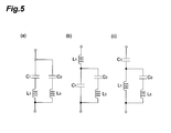
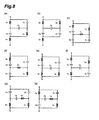
- FIG. 5 are diagrams illustrating examples of the circuit configuration of the capacitance suppression element section that can reduce the influence of the parasitic capacitance up to a second-order harmonic of a clock frequency;
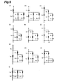
- FIG. 6 are diagrams illustrating examples of the circuit configuration of the capacitance suppression element section that can reduce the influence of the parasitic capacitance up to a third-order harmonic of the clock frequency;
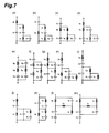
- FIG. 7 are diagrams illustrating other examples of the circuit configuration of the capacitance suppression element section that can reduce the influence of the parasitic capacitance up to the third-order harmonic of the clock frequency;
- FIG. 8 are diagrams illustrating still other examples of the circuit configuration of the capacitance suppression element section that can reduce the influence of the parasitic capacitance up to the third-order harmonic of the clock frequency;
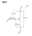
- FIG. 9 is a model diagram of a semiconductor switch element for simulations.
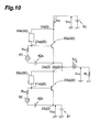
- FIG. 10 is a circuit diagram for simulations corresponding to the switching circuit shown in FIG. 1 ;
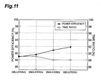
- FIG. 11 is a graph showing calculation results of power efficiency and time ratio in simulations according to the first embodiment
- FIG. 12 is a graph showing calculation results of total harmonic distortion (THD) in the simulations according to the first embodiment
- FIG. 13 is a circuit diagram illustrating the schematic configuration of a switching circuit according to a second embodiment
- FIG. 14 is a diagram for explaining the principle that a parasitic capacitance of a semiconductor switch element can be suppressed by connecting a capacitance element;
- FIG. 15 is a model diagram for simulations corresponding to the switching circuit shown in FIG. 13 ;
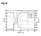
- FIG. 16 is a graph showing a simulation result of a case in which each of four semiconductor switch elements shown in FIG. 15 has all parasitic capacitances;
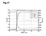
- FIG. 17 is a graph showing a simulation result of a case in which parasitic capacitances C GD of the four semiconductor switch elements shown in FIG. 15 are 0;
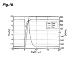
- FIG. 18 is a graph showing a simulation result of a case in which parasitic capacitances C GD of upper two semiconductor switch elements shown in FIG. 15 are 0;
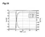
- FIG. 19 is a graph showing a simulation result of a case in which the parasitic capacitances C GD of the upper two semiconductor switch elements shown in FIG. 15 are 0, and the capacitance element is assumed to be connected.
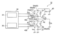
- FIG. 1 is a circuit diagram illustrating the schematic configuration of the switching circuit 10 according to the first embodiment.
- the switching circuit 10 includes a semiconductor switch element 20 a and a semiconductor switch element 20 b .
- the switching circuit 10 may include a drive circuit 30 that drives the respective semiconductor switch elements 20 a and 20 b.
- Both the semiconductor switch elements 20 a and 20 b are MOS field-effect transistors (MOSFET). Examples of the MOSFET include a power MOSFET.
- the semiconductor switch elements 20 a and 20 b have the same configuration and device characteristic. Please note that the semiconductor switch elements 20 a and 20 b may have different configurations and device characteristics.
- the semiconductor switch element 20 a has a gate terminal 21 a as an input terminal, a drain terminal 22 a as an output terminal, and a source terminal 23 a as a common terminal.
- the semiconductor switch element 20 b has a gate terminal 21 b as an input terminal, a drain terminal 22 b as an output terminal, and a source terminal 23 b as a common terminal.
- the drain terminal 22 a of the semiconductor switch element 20 a is connected to a first power source 40 .
- the first power source 40 supplies a positive voltage V DD to the drain terminal 22 a .
- the positive voltage V DD is 400 V, for example.
- the source terminal 23 a of the semiconductor switch element 20 a is connected to the drain terminal 22 b of the semiconductor switch element 20 b . In this case, the semiconductor switch element 20 a and the semiconductor switch element 20 b are connected in series.
- the source terminal 23 b of the semiconductor switch element 20 b is connected to a second power source 41 .
- the second power source 41 supplies a negative voltage V SS to the source terminal 23 b .
- the negative voltage V SS may be ⁇ V DD .
- a diode D 1 connected between the drain terminal 22 a and the source terminal 23 a of the semiconductor switch element 20 a , and a diode D 2 connected between the drain terminal 22 b and the source terminal 23 b of the semiconductor switch element 20 b represent parasitic diodes of the semiconductor switch elements 20 a and 20 b .
- the diodes D 1 and D 2 are described as the parasitic diodes since the semiconductor switch elements 20 a and 20 b are the MOS field-effect transistors.
- the diodes D 1 and D 2 may be connected to the semiconductor switch elements 20 a and 20 b as protective diodes.
- cathode terminals of the diodes D 1 and D 2 are respectively connected to the drain terminals 22 a and 22 b
- anode terminals of the diodes D 1 and D 2 are respectively connected to the source terminals 23 a and 23 b as shown in FIG. 1 . Since the diodes D 1 and D 2 are described as the parasitic diodes of the semiconductor switch elements 20 a and 20 b in the present embodiment, the description thereof may be sometimes omitted.
- the drive circuit 30 is a gate drive circuit that performs pulse width modulation (PWM) control of the respective semiconductor switch elements 20 a and 20 b .
- the drive circuit 30 is connected to the respective gate terminals (the input terminals) 21 a and 21 b of the semiconductor switch elements 20 a and 20 b .
- the drive circuit 30 supplies a PWM signal as a positive-phase pulse-like signal to the gate terminal 21 a of the semiconductor switch element 20 a , and also supplies a PWM signal as a negative-phase pulse-like signal to the gate terminal 21 b of the semiconductor switch element 20 b .
- the PWM signal has a modulation frequency f M and a clock frequency f CLK as a switching frequency for switching each of the semiconductor switch elements 20 a and 20 b .
- the PWM signal can be generated by comparing a signal wave (e.g., a sine wave) having the modulation frequency f M and a triangle wave having the clock frequency f CLK by a comparator or the like.
- a signal wave e.g., a sine wave
- a triangle wave having the clock frequency f CLK
- the first and second drive circuit sections 31 and 32 are respectively connected to negative poles of third power sources 42 a and 42 b .
- Positive poles of the third power sources 42 a and 42 b are respectively connected to the source terminals 23 a and 23 b of the semiconductor switch elements 20 a and 20 b .
- the third power sources 42 a and 42 b supply predetermined negative voltages (e.g., ⁇ 11 V) based on the source terminals 23 a and 23 b to the first and second drive circuit sections 31 and 32 .
- an inductance element L L as an inductive load is connected to a connection point between the source terminal 23 a of the semiconductor switch element 20 a and the drain terminal 22 b of the semiconductor switch element 20 b .
- a resistance R L whose one end is grounded is connected to the other end of the inductance element L L .
- An element value of the inductance element L L is 2.5 mH, for example.
- a resistance value of the resistance R L is 10 ⁇ , for example.
- the pulse-like signal is supplied between the gate terminal 21 a and the source terminal 23 a from the first drive circuit section 31 .
- the semiconductor switch element 20 a is thereby controlled between an ON state in which a current flows between the drain terminal 22 a and the source terminal 23 a , and an OFF state in which no current flows between the drain terminal 22 a and the source terminal 23 a according to switching of the PWM signal as the pulse-like signal between a Hi level and a Low level.
- the semiconductor switch element 20 b that is, when the PWM signal is supplied to the gate terminal 21 b from the second drive circuit section 32 , the semiconductor switch element 20 b can be controlled between the ON state and the OFF state.
- the PWM signal supplied to the semiconductor switch element 20 a from the first drive circuit section 31 has a positive phase. Meanwhile, the PWM signal supplied to the semiconductor switch element 20 b from the second drive circuit section 32 has a negative phase.
- the semiconductor switch element 20 a is in the ON state
- the semiconductor switch element 20 b is in the OFF state.
- a current flows from the drain terminal 22 a to the source terminal 23 a . Since the semiconductor switch element 20 b is in the OFF state, the current flows toward a coil as the inductance element L L .
- the semiconductor switch element 20 b is in the ON state.
- the current from the semiconductor switch element 20 a does not flow to the inductance element L L
- a current flows between the drain terminal 22 b and the source terminal 23 b of the semiconductor switch element 20 b .
- the current flows from the inductance element L L to the semiconductor switch element 20 b .
- the direction of the current flowing through the inductance L L is switched as indicated by arrows A 1 and A 2 in FIG. 1 .
- capacitance suppression element sections 50 a and 50 b are connected to the semiconductor switch elements 20 a and 20 b so as to increase the switching speed of each of the semiconductor switch elements 20 a and 20 b and improve the power efficiency of the switching circuit 10 .
- the capacitance suppression element sections 50 a and 50 b are element sections that suppress the influence of parasitic capacitance existing in each of the semiconductor switch elements 20 a and 20 b.
- the capacitance suppression element sections 50 a and 50 b will be described. Since the semiconductor switch elements 20 a and 20 b have the same configuration as described above in the present embodiment, the semiconductor switch elements 20 a and 20 b are referred to as semiconductor switch element 20 except when the semiconductor switch elements 20 a and 20 b are separately described. The same applies to the description of each terminal of the semiconductor switch elements 20 a and 20 b . Since the semiconductor switch elements 20 a and 20 b have the same configuration, the capacitance suppression element sections 50 a and 50 b may also have the same configuration. Thus, the capacitance suppression element sections 50 a and 50 b are referred to as capacitance suppression element section 50 except when the capacitance suppression element sections 50 a and 50 b are separately described.
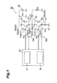
- FIG. 2 is a diagram for explaining the relationship between the parasitic capacitance existing in the semiconductor switch element and the capacitance suppression element section.
- parasitic capacitances C GS , C GD , and C DS exist between the respective terminals of the semiconductor switch element 20 .
- the parasitic capacitances C GS , C GD , and C DS are shown as capacitance elements.
- At least one capacitance suppression element section 50 is connected to the semiconductor switch element 20 so as to suppress at least one of the parasitic capacitances C GS , C GD , and C DS .
- the capacitance suppression element section 50 is connected between the terminals where the parasitic capacitance C GS , C OD , or C DS to be suppressed exists.
- the capacitance suppression element section 50 is connected in parallel with the parasitic capacitance C GS , C GD , or C DS to be suppressed.
- FIG. 2 shows one example in which the capacitance suppression element section 50 is connected between the gate terminal 21 and the drain terminal 22 to suppress the parasitic capacitance C GD .
- the parasitic capacitance to be suppressed by the capacitance suppression element section 50 out of the parasitic capacitances C GS , C GD , and C DS is referred to as parasitic capacitance C X .
- the capacitance suppression element section 50 suppresses the parasitic capacitance C X of the semiconductor switch element 20 at a frequency N times as high as the clock frequency of the PWM signal.
- the capacitance suppression element section 50 is configured to satisfy following conditions.
- An impedance of the parasitic capacitance C X and an impedance of the capacitance suppression element section 50 are equal in magnitude to each other, and have opposite signs from each other at an angular frequency of an N-th order harmonic of the clock frequency of the PWM signal.
- An output impedance R CO of the drive circuit 30 connected to the gate terminal 21 of the semiconductor switch element 20 is sufficiently smaller than an input impedance of the semiconductor switch element 20 .
- the output impedance R CO with respect to the semiconductor switch element 20 a is an output impedance of the first drive circuit section 31 , and corresponds to a resistance value of a resistance R CO shown between the first drive circuit section 31 and the source terminal 23 a .
- the output impedance R CO with respect to the semiconductor switch element 20 b is an output impedance of the second drive circuit section 32 , and corresponds to a resistance value of a resistance R CO shown between the second drive circuit section 32 and the source terminal 23 b.
- a reactance of the capacitance suppression element section 50 is X( ⁇ ) as a function of an angular frequency ⁇
- the above (i) is expressed by an expression (5)
- the above (ii) is expressed by an expression (6). That is, the capacitance suppression element section 50 is configured to satisfy the expressions (5) and (6).
- X( ⁇ ) is also referred to as reactance curve of the capacitance suppression element section 50 .
- ⁇ represents an imaginary unit
- ⁇ 0 represents a product of the clock frequency f CLK of the PWM signal and 2 ⁇
- ⁇ M represents a product of the modulation frequency f M of the PWM signal and 2 ⁇
- C X represents the parasitic capacitance between the terminals of the semiconductor switch element 20 where the capacitance suppression element section 50 is connected.
- C X C GD .
- R CO represents the output impedance of the drive circuit 30 connected to the gate terminal 21 of the semiconductor switch element 20 .
- ⁇ may be sufficiently greater than 1.
- a may be 10 or more, or may be 100 or more.
- the capacitance suppression element section 50 When the capacitance suppression element section 50 is connected between the terminals where the parasitic capacitance C X to be cancelled exists out of the parasitic capacitances C GS , C GD , and C DS between the terminals of the semiconductor switch element 20 , the capacitance suppression element section 50 is connected in parallel with the parasitic capacitance C X .
- the capacitance suppression element section 50 satisfies the expressions (5) and (6), a combined impedance of the capacitance suppression element section 50 and the parasitic capacitance C X in parallel therewith has a very high value (e.g., an infinity ⁇ ) at the N-th order harmonic of the clock frequency f CLK of the PWM signal.
- the semiconductor switch element 20 to which the capacitance suppression element section 50 satisfying the expression (5) is connected can operate as in a case in which the parasitic capacitance C X between the terminals where the capacitance suppression element section 50 is connected practically does not exist. That is, the capacitance suppression element section 50 can reduce the parasitic capacitance C X of the semiconductor switch element 20 in the operation of the semiconductor switch element 20 .
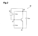
- FIG. 3 is a graph showing the relationship between a reactance curve of the capacitance suppression element section and a reactance curve of the parasitic capacitance, and corresponds to the relationship of the expression (5).
- a horizontal axis represents an angular frequency ⁇
- a vertical axis represents a reactance [ ⁇ ].
- a solid line in FIG. 3 represents the reactance curve X( ⁇ ) of the capacitance suppression element section 50 .
- An dashed dotted line in FIG. 3 represents the reactance curve (1/ ⁇ C X ) of the parasitic capacitance.
- the reactance curve of the parasitic capacitance C X is a curve representing an absolute value of a reactance of the parasitic capacitance C X
- the reactance function X( ⁇ ) of the capacitance suppression element section 50 having the minimum number of elements constituting the capacitance suppression element section 50 can satisfy an expression (7).
- ⁇ pt , ⁇ z0 , and ⁇ zt are values determined so as to satisfy 0 ⁇ z0 ⁇ 0 , and t ⁇ 0 ⁇ pt ⁇ zt ⁇ (t+1) ⁇ 0 , and also satisfy the expressions (5) and (6), and ⁇ is any value determined so as to satisfy the expressions (5) and (6).
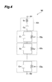
- FIG. 4 is a diagram illustrating one example of the circuit configuration of the capacitance suppression element section 50 that satisfies the expression (7).
- the capacitance suppression element section 50 has N circuit sections of first to N-th circuit sections 53 1 to 53 N connected in series between terminals 51 and 52 of the capacitance suppression element section 50 .
- the first circuit section 53 1 is obtained by connecting a capacitance element C 0 and an inductance element L 0 in series.
- the first circuit section 53 1 is a series circuit.
- the capacitance suppression element section 50 may be composed only of the first circuit section 53 1 .
- an i-th circuit section 53 i (i is an integer of 2 to N) out of the second to N-th circuit sections 53 2 to 53 N is obtained by connecting a capacitance element C i-1 and an inductance element L i-1 in parallel.
- the i-th circuit section 53 i constitutes a parallel resonant circuit.
- the circuit configuration shown in FIG. 4 is also referred to as basic configuration for the purpose of description. In the basic configuration, the parasitic capacitance can be reduced with respect to another harmonic by increasing the parallel resonant circuit by one stage as shown in FIG. 4 .
- the parasitic capacitance when the parasitic capacitance can be reduced with respect to the N-th order harmonic, the parasitic capacitance can be also reduced with respect to any harmonic other than the N-th order harmonic by increasing the number of stages of the parallel resonant circuit. It is not necessary to reduce the parasitic capacitance sequentially from a lowest order harmonic. It is also not necessary to reduce the parasitic capacitance only with respect to a next-order harmonic. For example, the parasitic capacitance may be reduced with respect to harmonics of every two orders such as odd orders of 1, 3, 5, 7 and so on.
- the expression (5) is expressed as expressions (8 0 ) to (8 N-1 ).
- the expression (7) can be transformed into an expression (9).
- L 1 1/(C 1 ( ⁇ p1 ) 2
- L 2 1 /(C 2 ( ⁇ p2 ) 2
- L N-1 1/(C N-1 ( ⁇ p(N-1) ) 2 ).
- An expression (10) is obtained by substituting the expression (9) into the expressions (8 0 ) to (8 N-1 ) and the expression (6), and thereafter performing a matrix calculation.
- ⁇ p1 to ⁇ p(N-1) is given within a range of 0 ⁇ z0 ⁇ 0 , and t ⁇ 0 ⁇ pt ⁇ zt ⁇ (t+1) ⁇ 0 (t is an integer of 1 to N ⁇ 1).
- t is an integer of 1 to N ⁇ 1).
- L 0 , C 0 , L 1 , C 1 , L 2 , and C 2 are as follows.
- ⁇ , ⁇ z0 , and ⁇ z1 can be also obtained.
- One example of a method for obtaining ⁇ , ⁇ z0 , and ⁇ z1 will be described.
- ⁇ , ⁇ z0 , ⁇ z1 , and ⁇ z2 can be obtained based on the expressions (15a) to (15d) and the calculated L 0 , C 0 , L 1 , C 1 , L 2 , and C 2 .
- FIG. 4 one example of the element configuration of the capacitance suppression element section 50 has been described by reference to FIG. 4 .
- the configuration of the capacitance suppression element section 50 is not limited to that in FIG. 4 .
- C 0 , C 1 , C 2 , L 0 , L 1 , and L 2 are assigned to capacitance elements and inductance elements in a similar manner to the case in FIG. 4 .
- Element values of the elements are determined so as to satisfy the expressions (5) and (6).
- the capacitance suppression element section 50 includes six reactance elements.
- the capacitance suppression element section 50 includes at least six reactance elements.
- the expression (16) may also include the circuit configuration in FIG. 6( a ).
- an expression corresponding to the element configuration in FIG. 6( a ) is as in an expression (18).
- C 0 , C 1 , C 2 , L 0 , L 1 , and L 2 are assigned to the capacitance elements and the inductance elements in FIG. 6( a ) in a similar manner to the case in FIG. 4 .
- C 0 , C 1 , C 2 , L 0 , L 1 , and L 2 are represented as C 0a , C 1a , C 2a , L 0a , L 1a , and L 2a so as to be distinguished from the case in FIG. 4 .
- the right-hand side of the expression (16) is transformed into the right-hand side of the expression (18) so as to obtain the respective element values.
- expressions (20a) to (20f), expressions (21a) to (21g), and expressions (22a) to (22d) can be obtained.
- the element values of the respective elements in the case of the circuit configuration shown in FIG. 6( a ), that is, L 0a , C 0a , L 1a , C 1a , L 2a , and C 2a can be obtained.
- a 3 , a 2 , a 1 , a 0 , b 2 , b 1 , and b 0 are obtained by the expressions (17a) to (17g).
- the element values of the elements of other circuit configurations such as the respective circuit configurations shown in FIGS. 5( a ) to 5 ( c ) may be similarly obtained. That is, the expression (11) is transformed so as to represent the characteristics of the respective circuit configurations.
- the element values of the respective circuit configurations can be obtained by using a 3 , a 2 , a 1 , a 0 , b 2 , b 1 , and b 0 obtained by comparison of rational function coefficients before and after the expression transformation.
- the element values may be also determined by using a numerical analytical method.
- the respective element values of the capacitance suppression element section 50 are determined by assuming the circuit configuration as shown in FIG. 4 or the like.
- the circuit configuration of the capacitance suppression element section 50 may be designed so as to satisfy the expressions (5) and (6).
- the circuit configuration may be determined by a topology search method, for example.
- One example of a method for determining the circuit configuration by the topology search method is as follows.
- a polynomial expression expressed as a n (s 2 ) n +a n-1 (s 2 ) n-1 + . . . +a 0 is defined as D n .
- s j ⁇ .
- n (p 2 ) n +a n-1 (p 2 ) n-1 + . . . +a 0 is defined as D n .
- p 1/s.
- the circuit structure is obtained by applying following rules.
- arrows indicate the direction of expression transformation.
- the rule 5 indicates that s and 1/p can be mutually converted to each other.
- the right-hand side of the expression (28) can be transformed as follows by applying the rules 1 to 4 a plurality of times.
- the number of elements of the capacitance suppression element section 50 is determined by the order of the harmonic to be suppressed, i.e., the value of N.
- the number of capacitance elements and the number of inductance elements are equal to each other.
- the capacitance elements and the inductance elements may be arranged according to following rules.
- Rule A Opposite ends of each element are connected to separate relay nodes or terminals.
- Rule B Three or more elements are not connected in parallel between two nodes.
- Rule C The same applies to a dual of the rule B.
- Rule D A closed path in which only two elements are connected in series from one node and return to the same node is not formed.
- Rule E When a plurality of partial two-terminal circuits are connected in series, the circuits in different order are regarded as the same circuits.
- Rule F A circuit in which one element is connected in parallel with remaining elements between the opposite terminals of the capacitance suppression element section 50 is excluded.
- the circuit configuration of the capacitance suppression element section 50 can be determined more quickly by applying the above rules A to F.
- the capacitance suppression element section 50 is connected to the semiconductor switch element 20 .
- the capacitance suppression element section 50 is designed so as to satisfy the expressions (5) and (6) as described above. It is thus considered that the parasitic capacitance C X practically does not exist between the terminals of the semiconductor switch element 20 where the capacitance suppression element section 50 is connected up to the N-th order harmonic of the clock frequency f CLK of the PWM signal. That is, the parasitic capacitance C X is neutralized by the capacitance suppression element section 50 . A time required to charge and discharge the parasitic capacitance C X can be thereby reduced, so that switching is performed at higher speed in the semiconductor switch element 20 . As a result, the switching speed of the switching circuit 10 can be increased, and the power efficiency of the switching circuit 10 can be improved.
- the capacitance suppression element section 50 a is connected between the gate terminal 21 a and the drain terminal 22 a of the semiconductor switch element 20 a .
- the parasitic capacitance C GD of the semiconductor switch element 20 a can be cancelled.
- the parasitic capacitance C GD of the semiconductor switch element 20 b can be cancelled by the capacitance suppression element section 50 b.
- Overdrive may be performed as a method for increasing the switching speed of the switching circuit 10 using the semiconductor switch element 20 .
- the configuration of the drive circuit 30 may become complicated so as to perform the overdrive as compared to a case in which the overdrive is not performed.
- the drive circuit 30 also needs to have a higher ampacity so as to perform the overdrive. Accordingly, the drive circuit 30 may be increased in size, or the power efficiency of the switching circuit 10 including the drive circuit 30 may be reduced as compared to the case in which the overdrive is not performed. In this case, even when the high-speed switching is achieved by the overdrive, an improvement in the power efficiency by the high-speed switching itself may not be obtained.
- the capacitance suppression element section 50 neutralizes the parasitic capacitance C X itself to achieve the high-speed switching. Accordingly, the switching speed of the switching circuit 10 can be increased and the power efficiency can be improved as described above without performing the overdrive.
- the capacitance suppression element section 50 can achieve the state in which the parasitic capacitance C X practically does not exist in the present embodiment, the capacitance suppression element section 50 only needs to reduce the influence of the parasitic capacitance C X when the capacitance suppression element section 50 is connected.
- the circuit configuration of the capacitance suppression element section 50 and the element values of the elements of the capacitance suppression element section 50 may be set to values with which an equivalent capacitance of the terminal value where the capacitance suppression element section 50 is connected becomes 1/10 or less of the original parasitic capacitance C X by connecting the capacitance suppression element section 50 .
- the element values of the elements of the capacitance suppression element section 50 may be also set to values with which the equivalent capacitance becomes half or less of the original parasitic capacitance C X .
- the switching circuit 10 includes the inductance element L L as the inductive load as one example in the present embodiment.
- the switching circuit 10 can be used for an inverter or the like.
- the switching circuit 10 can be used for driving the motor.
- FIG. 9 is a diagram illustrating a model of a semiconductor switch element for simulations.
- a MOS field-effect transistor was assumed to be used as the semiconductor switch element 20 . It was assumed that parasitic resistances R G and R I existed in addition to the parasitic capacitances C GS , C DS , and C GD in the semiconductor switch element 20 .
- FIG. 10 is a circuit diagram for simulations corresponding to the switching circuit 10 shown in FIG. 1 .
- elements corresponding to those in FIG. 1 are assigned the same reference numerals for the convenience of description.
- the first drive circuit section 31 and the second drive circuit section 32 of the drive circuit 30 shown in FIG. 1 are shown as signal sources 61 and 62 respectively corresponding to the semiconductor switch elements 20 a and 20 b .
- the semiconductor switch elements 20 a and 20 b respectively have the configuration shown in FIG. 9 .
- Element values or the like in a simulation circuit model shown in FIG. 10 were set as follows.
- Modulation frequency f M of the PWM signal supplied from the signal sources 61 and 62 60 kHz
- Resistance value of the resistance R CO (Output impedance R CO of the signal sources 61 and 62 from the gate terminals 21 a and 21 b ): 30 ⁇
- Negative voltage V SS supplied to the source terminal 23 b ⁇ 400 V
- the basic configuration shown in FIG. 4 was employed for the capacitance suppression element sections 50 a and 50 b .
- the power efficiency was calculated by (output voltage V out ⁇ output current I out )/(supply voltage V DD ⁇ supply current I EE ) ⁇ 100(%).
- the output current I out is a current flowing through the inductance L L .
- the supply current I EE is a current flowing into the drain terminal 22 a.
- the power efficiency in this case was 96%.
- the power efficiency in this case was 89%.
- simulations 2a to 2c were performed such that the parasitic capacitance C GD was suppressed by use of the capacitance suppression element section 50 by setting the values of the parasitic capacitances C GD , C GS , and C DS of the semiconductor switch element 20 to the values indicated as the device parameters above.
- a simulation 2d was also performed for comparison as a case in which the capacitance suppression element section 50 was not connected.
- Total harmonic distortion (MD) was also calculated so as to examine the influence of the capacitance suppression element section on the THD.
- the simulation was performed for the case in which the capacitance suppression element section 50 was not connected, and power efficiency and time ratio were calculated.
- FIG. 11 is a graph showing the calculation results of the power efficiency and the time ratio in the simulations 2a to 2d.
- a horizontal axis represents the performed simulations.
- a vertical axis represents the power efficiency (%) and the time ratio (%).
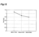
- FIG. 12 is a graph showing the calculation results of the THD in the simulations 2a, 2b, and 2c.
- a horizontal axis represents the performed simulations.
- a vertical axis represents the total harmonic distortion: THD (%).
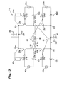
- FIG. 13 is a circuit diagram illustrating the schematic configuration of a switching circuit according to a second embodiment of the present invention.
- a switching circuit 70 is a differential switching circuit.
- the switching circuit 70 includes four semiconductor switch elements 20 a , 20 b , 20 c , and 20 d . All the semiconductor switch elements 20 a to 20 d are the same semiconductor switch element as that of the first embodiment. In the following description, the semiconductor switch elements 20 a to 20 d may be sometimes referred to as semiconductor switch element 20 in a similar manner to the case of the first embodiment.
- the switching circuit 70 may include drive circuits 30 a , 30 b , 30 c , and 30 d that respectively supply PWM signals to gate terminals 21 a , 21 b , 21 c , and 21 d of the semiconductor switch elements 20 a , 20 b , 20 c , and 20 d .
- the drive circuits 30 a , 30 b , 30 c , and 30 d are respectively connected to the four semiconductor switch elements 20 a , 20 b , 20 c , and 20 d in FIG. 11 , only one drive circuit 30 may be employed as in the case of the first embodiment.
- the drive circuit 30 a and the drive circuit 30 b correspond to the first drive circuit section 31 and the second drive circuit section 32 .
- a drain terminal (an output terminal) 22 a of the semiconductor switch element (a first semiconductor switch element) 20 a and a drain terminal (an output terminal) 22 c of the semiconductor switch element (a third semiconductor switch element) 20 c are connected to each other.
- a source terminal (a common terminal) 23 b of the semiconductor switch element (a second semiconductor switch element) 20 b and a source terminal (a common terminal) 23 d of the semiconductor switch element (a fourth semiconductor switch element) 20 d are connected to each other.
- a first power source 40 and a second power source 41 are respectively connected to a connection point between the drain terminal 22 a and the drain terminal 22 c , and a connection point between the source terminal 23 b and the source terminal 23 d .
- the first power source 40 supplies a positive voltage V DD to the drain terminals 22 a and 22 c .
- the second power source 41 supplies a negative voltage V SS to the source terminals 23 b and 23 d.
- the semiconductor switch elements 20 a and 20 b are connected in series in a similar manner to the first embodiment.
- the semiconductor switch elements 20 c and 20 d are also connected in series. That is, a source terminal 23 c of the semiconductor switch element 20 c and a drain terminal 22 d of the semiconductor switch element 20 d are connected to each other.
- a connection point between a source terminal 23 a and a drain terminal 22 b , and a connection point between the source terminal 23 c and the drain terminal 22 d are connected via a load 80 .
- the load 80 may be an inductive load such as an inductance element in a similar manner to the first embodiment, or may be a resistive load. For example, when a motor is connected as the load 80 , the motor may be driven.
- the drive circuits 30 a and 30 d respectively supply positive-phase PWM signals to the gate terminals 21 a and 21 d of the semiconductor switch elements 20 a and 20 d .
- the drive circuits 30 b and 30 c respectively supply negative-phase PWM signals to the gate terminals 21 b and 21 c of the semiconductor switch elements 20 b and 20 c .
- the PWM signals supplied to the gate terminals 21 a to 21 d have the same clock frequency f CLK .
- Resistances R CO between the respective semiconductor switch elements 20 a to 20 d and the corresponding drive circuits 30 a to 30 d represent output impedances of the drive circuits 30 a to 30 d respectively connected to the gate terminals 21 a to 21 d of the semiconductor switch elements 20 a to 20 d .
- Third power sources 42 a to 42 d are respectively connected between the source terminals 23 a to 23 d of the semiconductor switch elements 20 a to 20 d and the drive circuits 30 a to 30 d .
- Positive poles of the third power sources 42 a to 42 d are connected to the corresponding source terminals 23 a to 23 d .
- Negative poles of the third power sources 42 a to 42 d are connected to the corresponding drive circuits 30 a to 30 d . Accordingly, predetermined negative voltages based on the source terminals 23 a to 23 d are supplied to the drive circuits 30 a to 30 d in a similar manner to the first embodiment.
- the magnitude of the predetermined negative voltage may be equal to that of the negative voltage supplied from the third power source 42 a or 42 b in the first embodiment.
- the drive circuits 30 a and 30 d supply the positive-phase PWM signals to the semiconductor switch elements 20 a and 20 d
- the drive circuits 30 b and 30 c supply the negative-phase PWM signals to the semiconductor switch elements 20 b and 20 c .
- the semiconductor switch elements 20 a and 20 d are in an ON state
- the semiconductor switch elements 20 b and 20 c are in an OFF state.
- a current flows in the direction of an arrow B 1 in FIG. 13 .
- the semiconductor switch elements 20 a and 20 d are in the OFF state
- the semiconductor switch elements 20 b and 20 c are in the ON state.
- a current flows in the direction of an arrow B 2 in FIG. 13 . Accordingly, the direction of a current flowing through the load 80 can be switched according to the PWM signals.
- capacitance suppression element sections 50 a and 50 c are connected, at least one by one, to the semiconductor switch elements 20 a and 20 c so as to suppress at least one of three parasitic capacitances C GS , C GD , and C DS of the semiconductor switch elements 20 a and 20 c .
- the capacitance suppression element sections 50 a and 50 c are respectively connected between the terminals where a parasitic capacitance C X to be suppressed exists.
- FIG. 13 shows a configuration in which the capacitance suppression element sections 50 a and 50 c are respectively connected between the gate terminals 21 a and 21 c and the drain terminals 22 a and 22 c of the semiconductor switch elements 20 a and 20 c .
- the capacitance suppression element sections 50 a and 50 c have the same circuit configuration as that of the first embodiment, the description thereof is omitted.
- the capacitance suppression element sections 50 a and 50 c may be sometimes referred to as capacitance suppression element section 50 in a similar manner to the case of the first embodiment.
- capacitance elements 90 and 91 are further respectively connected between the drain terminal 22 b of the semiconductor switch element 20 b and the gate terminal 21 d of the semiconductor switch element 20 d , and between the gate terminal 21 b of the semiconductor switch element 20 b and the drain terminal 22 d of the semiconductor switch element 20 d .
- a capacitance C 90 of the capacitance element (a first capacitance element) 90 is substantially equal to the parasitic capacitance C GD between the gate terminal 21 d and the drain terminal 22 d of the semiconductor switch element 20 d at an N-th order harmonic of the PWM signal.
- a capacitance C 91 of the capacitance element (a second capacitance element) 91 is substantially equal to the parasitic capacitance C GD between the gate terminal 21 b and the drain terminal 22 b of the semiconductor switch element 20 b.
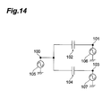
- FIG. 14 is a diagram for explaining the principle that the parasitic capacitance of the semiconductor switch element can be suppressed by connecting the capacitance element.
- FIG. 14 is a model diagram for calculating a capacitance component anticipated from the gate terminal 21 d in the semiconductor switch element 20 d having a differential circuit.
- a capacitance element 102 is connected between a first terminal 100 and a second terminal 101 , and a capacitance element 104 having the same capacitance as that of the capacitance element 102 is connected between the first terminal 100 and a third terminal 103 .
- the capacitance element 102 represents the parasitic capacitance C GD
- the capacitance element 104 corresponds to the capacitance element 90 .
- a signal source 105 is connected to the first terminal 100
- voltage sources 106 and 107 are respectively connected to the second terminal 101 and the third terminal 103 .
- the first terminal 100 corresponds to the gate terminal 21 d of the semiconductor switch element 20 d .
- the signal source 105 supplies a gate voltage V X to the first terminal 100 so as to represent the input of the PWM signal into the gate terminal 21 d .
- the second terminal 101 corresponds to the drain terminal 22 d of the semiconductor switch element 20 d .
- the voltage source 106 supplies a voltage V D to the second terminal 101 so as to represent the voltage of the drain terminal 22 d .
- the third terminal 103 corresponds to the drain terminal 22 b of the semiconductor switch element 20 b .
- a drain potential of the drain terminal 22 b of the semiconductor switch element 20 b is opposite to a drain potential of the drain terminal 22 d of the semiconductor switch element 20 d .
- a drain voltage ( ⁇ V D ) is supplied to the third terminal 103 from the voltage source 107 .
- the parasitic capacitance C GD between the gate and the drain equivalently does not exist, and it appears that a capacitance having the value of 2C GD exists between the gate terminal 21 d and the ground (that is, the source terminal).
- the influence of the parasitic capacitance C GD of the semiconductor switch element 20 d can be neutralized or cancelled.
- the semiconductor switch element 20 d has been mainly described here, the same applies to the semiconductor switch element 20 b . That is, when the capacitance element 91 is provided as shown in FIG. 13 , the influence of the parasitic capacitance C GD of the semiconductor switch element 20 b can be neutralized or cancelled at the N-th order harmonic of the PWM signal.
- the parasitic capacitance C GD between the gate and the drain affects the switching speed the most in the semiconductor switch elements 20 a to 20 d .
- the switching speeds of the semiconductor switch elements 20 b and 20 d can be increased.
- the capacitance elements 90 and 91 neutralize the influence of the parasitic capacitance C GD
- the capacitance elements 90 and 91 only need to reduce or suppress the influence of the parasitic capacitance C GD .
- the capacitances of the capacitance elements 90 and 91 may be set to values with which an equivalent capacitance becomes 1/10 or less of the original parasitic capacitance C X by connecting the capacitance elements 90 and 91 as described in the first embodiment.
- the capacitances of the capacitance elements 90 and 91 may be also set to values with which the equivalent capacitance becomes half or less of the original parasitic capacitance C X .
- the capacitance suppression element sections 50 a and 50 c reduce the influence of the parasitic capacitance C GD with respect to the semiconductor switch elements 20 a and 20 c .
- the capacitance elements 90 and 91 reduce the influence of the parasitic capacitance C GD with respect to the semiconductor switch elements 20 b and 20 d .
- the switching speeds of the semiconductor switch elements 20 a to 20 d can be increased, and the power efficiency can be improved in a similar manner to the case of the first embodiment.
- the switching speed and the power efficiency can be improved without performing overdrive in a similar manner to the case of the first embodiment.
- the capacitance elements 90 and 91 are used to reduce the influence of the parasitic capacitance C GD with respect to the semiconductor switch elements 20 b and 20 d , the switching circuit 70 can be more easily designed. Accordingly, the configuration of the switching circuit 70 is more effectively employed when there is a difference in device parameters of the semiconductor switch elements 20 a to 20 d.
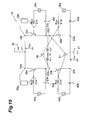
- FIG. 15 is a model diagram for simulations corresponding to the switching circuit 70 shown in FIG. 13 .
- the load 80 is represented by a series circuit of an inductance element L L1 , a resistance R L , and an inductance element L L2 .
- a voltage to the ground of the connection point between the source terminal 23 a of the semiconductor switch element 20 a and the drain terminal 22 b of the semiconductor switch element 20 b was set as an output voltage V out .
- the semiconductor switch elements 20 a to 20 d had the configuration shown in FIG. 9 in a similar manner to the first embodiment.
- the device parameters of the semiconductor switch elements 20 a to 20 d were the same as the device parameters described in the first embodiment.
- the capacitance elements 90 and 91 had a capacitance of 63 pF similarly to the capacitance C GD .
- Element values or the like in the simulation circuit model shown in FIG. 15 were set as follows.
- Modulation frequency f M of the PWM signal supplied from the drive circuits 30 a to 30 d 60 kHz
- Negative voltage V SS supplied to the source terminals 23 b and 23 d ⁇ 400 V
- the simulation was performed by assuming a case in which none of the capacitance elements 90 and 91 and the capacitance suppression element sections 50 a and 50 c was connected. In the simulation, all the parasitic capacitances of each of the semiconductor switch elements 20 a to 20 d were set to the values indicated as the device parameters.
- the simulation was performed by assuming a case in which the parasitic capacitance C GD between the gate and the drain of each of the semiconductor switch elements 20 was cancelled by the capacitance elements 90 and 91 and the capacitance suppression element sections 50 a and 50 c .
- the parasitic capacitance C GD of each of the semiconductor switch elements 20 a to 20 d was set to 0 as an ideal state.
- the simulation was performed by assuming that the parasitic capacitances C GD of the semiconductor switch elements 20 a to 20 d were neutralized by the capacitance suppression element sections 50 without providing the capacitance elements 90 and 91 .
- the parasitic capacitance C GD was set to 0.
- the simulation was performed on the same conditions as the simulation 3 except that the capacitance elements 90 and 91 were connected.
- FIGS. 16 to 19 are graphs respectively showing the results of the simulations 3 to 6.
- FIGS. 16 to 19 show changes in voltages V GS1a and V GS2a between the gate and the source of the semiconductor switch element 20 and the output voltage V out with respect to time.
- a horizontal axis represents the time [ ⁇ s]
- a vertical axis represents the voltages V GS [V] between the gate and the source and the output voltage V out [V].
- FIGS. 16 to 19 show V GSa as V GS in the semiconductor switch element 20 a at an upper left position in FIG. 15 , V GSb as V GS in the semiconductor switch element 20 b at a lower left position in FIG. 15 , and the output voltage V out as the voltage to the ground of the connection point between the semiconductor switch element 20 a and the semiconductor switch element 20 b.
- FIGS. 16 , 17 , and 18 it can be understood that there is a more rapid voltage change, particularly, a more rapid change in the output voltage V out than that in the case shown in FIG. 16 by providing the capacitance suppression element sections 50 a and 50 c and thereby cancelling the parasitic capacitances C GD of the semiconductor switch elements 20 a and 20 c , so that the results shown in FIG. 18 approaches to an ideal state shown in FIG. 17 .
- FIGS. 17 , 18 , and 19 it can be understood that there is a still more rapid voltage change, particularly, a still more rapid change in the output voltage V out than that in the case shown in FIG. 18 by providing the capacitance suppression element sections 50 and also connecting the capacitance elements, so that the results shown in FIG. 19 approaches to an ideal state shown in FIG. 17 .
- the capacitance suppression element section may be also used to reduce the parasitic capacitance with respect to the semiconductor switch elements 20 b and 20 d instead of the capacitance elements 90 and 91 .
- the influence of the capacitance having the value of 2C GD as the capacitance between the gate terminals 21 d and 21 b and the grounds (the source terminals) appearing to equivalently exist by the capacitance elements 90 and 91 may be substantially reduced by further connecting the capacitance suppression element section.
- At least one of the parasitic capacitances C X of the semiconductor switch elements 20 b and 20 d may be reduced by combination of the capacitance suppression element section and the capacitance elements 90 and 91 .
- the semiconductor switch element of the switching circuit is not limited to the MOS field-effect transistor described above.
- the semiconductor switch element may be an insulated gate bipolar transistor, a junction field-effect transistor, or a junction bipolar transistor.
- the semiconductor switch element may be a thyristor.
- the semiconductor switch element is the insulated gate bipolar transistor or the junction bipolar transistor, the semiconductor switch element has a gate terminal as the input terminal, a collector terminal as the output terminal, and an emitter terminal as the common terminal.
- the semiconductor switch element When the semiconductor switch element is the junction field-effect transistor, the semiconductor switch element has a gate terminal as the input terminal, a drain terminal as the output terminal, and a source terminal as the common terminal in a similar manner to the case of the MOS field-effect transistor.
- the semiconductor switch element When the semiconductor switch element is the thyristor, the semiconductor switch element has a gate terminal as the input terminal, an anode terminal as the output terminal, and a cathode terminal as the common terminal.
- the plurality of semiconductor switch elements of the switching circuit may have different configurations.
- the capacitance suppression element sections respectively connected to the plurality of semiconductor switch elements may also have different configurations.
- the number of semiconductor switch elements of the switching circuit is also not limited to 2 or 4 described above.
- the switching circuit only needs to have at least one semiconductor switch element.
- pulse-like signal supplied to the semiconductor switch element is the PWM signal in the various embodiments described above, any pulse-like signal may be employed as long as the ON/OFF switching of the semiconductor switch element can be controlled.
Landscapes
- Electronic Switches (AREA)
- Power Conversion In General (AREA)
- Semiconductor Integrated Circuits (AREA)
Abstract
Description
- This application claims priority to Provisional Application Ser. No. 61/493,823, filed on Jun. 6, 2011 and claims the benefit of Japanese Patent Application No. 2011-126337, filed on Jun. 6, 2011, all of which are incorporated herein by reference in their entirety.
- 1. Field
- Embodiments of the present invention relate to a switching circuit.
- 2. Description of the Related Art
- There are known switching circuits using semiconductor switch elements such as transistors (See Japanese Utility Model Publication No. Hei-07-47993). Since parasitic capacitance exists in the semiconductor switch element due to its configuration, a charge and discharge time of the parasitic capacitance is required when the semiconductor switch element performs a switching operation. As a method for reducing the charge and discharge time of the parasitic capacitance, the semiconductor switch element is overdriven in Japanese Utility Model Publication No. Hei-07-47993.
- In the overdrive, however, it is necessary to supply more voltage (or more current) than is required to drive the semiconductor switch element. Thus, the semiconductor switch element may be damaged in some cases, and the power efficiency of the switching circuit is easily reduced.
- It is an object of the present invention to provide a switching circuit which can increase a switching speed and can also improve power efficiency without performing overdrive.
- A switching circuit according to one aspect of the present invention is a switching circuit including at least one semiconductor switch element having an input terminal, an output terminal, and a common terminal, a pulse-like signal being applied between the input terminal and the common terminal to switch a current between the output terminal and the common terminal. The switching circuit further includes a capacitance suppression element section connected at least one of between the input terminal and the output terminal, between the input terminal and the common terminal, and between the output terminal and the common terminal. The capacitance suppression element section reduces a parasitic capacitance between the terminals of the semiconductor switch element where the capacitance suppression element section is connected to less than that obtained when the capacitance suppression element section is not connected at a frequency N times (N is an integer of 1 or more) as high as a clock frequency of the pulse-like signal.
- A switching circuit according to another aspect of the present invention is a switching circuit including four semiconductor switch elements each having an input terminal, an output terminal, and a common terminal, an output terminal of a first semiconductor switch element out of the four semiconductor switch elements and an output terminal of a third semiconductor switch element out of the four semiconductor switch elements being connected to each other, a common terminal of a second semiconductor switch element out of the four semiconductor switch elements and a common terminal of a fourth semiconductor switch element out of the four semiconductor switch elements being connected to each other, a common terminal of the first semiconductor switch element and an output terminal of the second semiconductor switch element being connected to each other, a common terminal of the third semiconductor switch element and an output terminal of the fourth semiconductor switch element being connected to each other, and a pulse-like signal being applied to each input terminal of the first to fourth semiconductor switch elements such that the second and third semiconductor switch elements are in an OFF state when the first and fourth semiconductor switch elements are in an ON state and the second and third semiconductor switch elements are in an ON state when the first and fourth semiconductor switch elements are in an OFF state. The switching circuit further includes a capacitance suppression element section connected at least one of between the input terminal and the output terminal, between the input terminal and the common terminal, and between the output terminal and the common terminal of at least one of the four semiconductor switch elements. The capacitance suppression element section reduces a parasitic capacitance between the terminals of the semiconductor switch element where the capacitance suppression element section is connected to less than that obtained when the capacitance suppression element section is not connected at a frequency N times (N is an integer of 1 or more) as high as a clock frequency of the pulse-like signal.
- In the configuration of the switching circuit according to the one aspect and the another aspect of the present invention, the influence of the parasitic capacitance itself existing in the semiconductor switch element is reduced by the capacitance suppression element section. Accordingly, a switching speed can be increased, and power efficiency can be improved without performing overdrive.
- The switching circuit according to the another aspect of the present invention may further include a first capacitance element connected between the output terminal of the second semiconductor switch element and the input terminal of the fourth semiconductor switch element, and a second capacitance element connected between the input terminal of the second semiconductor switch element and the output terminal of the fourth semiconductor switch element. In the aspect, the first capacitance element may have a capacitance to reduce a parasitic capacitance between the input terminal and the output terminal of the fourth semiconductor switch element to less than that obtained when the first capacitance element is not connected at a frequency N times (N is an integer of 1 or more) as high as the clock frequency of the pulse-like signal supplied to the fourth semiconductor switch element. The second capacitance element may have a capacitance to reduce a parasitic capacitance between the input terminal and the output terminal of the second semiconductor switch element to less than that obtained when the second capacitance element is not connected at a frequency N times (N is an integer of 1 or more) as high as the clock frequency of the pulse-like signal supplied to the second semiconductor switch element.
- In the configuration, since the first and second capacitance elements are connected, the parasitic capacitance between the input terminal and the output terminal of each of the second and fourth semiconductor switch elements can be reduced. As a result, the switching speed can be further increased and the power efficiency can be further improved.
- The pulse-like signal may be a PWM signal. In this case, the capacitance suppression element section may be configured to satisfy expressions (1) and (2) when a reactance of the capacitance suppression element section is a function X(ω) of an angular frequency.
-
- (In the expressions (1) and (2), j represents an imaginary unit, ω0, ωM represents a product of a clock frequency of the PWM signal and 2π, represents a product of a modulation frequency of the PWM signal and 2π, CX represents a parasitic capacitance between the terminals of the semiconductor switch element as the parasitic capacitance between the terminals of the semiconductor switch element where the capacitance suppression element section is connected, RCO represents an output impedance of a drive circuit that is connected to the input terminal of the semiconductor switch element where the capacitance suppression element section is connected and supplies the PWM signal.)
- In the configuration, a combined impedance of the parasitic capacitance between the terminals where the capacitance suppression element section is connected and the capacitance suppression element section becomes very large in the semiconductor switch element where the capacitance suppression element section is connected. As a result, the semiconductor switch element approaches a state in which the parasitic capacitance between the terminals where the capacitance suppression element section is connected practically does not exist. The influence of the parasitic capacitance can be thereby reduced.
- The function X(ω) may be expressed by an expression (3).
-
- (In the expression (3), when t is an integer of 1 to N−1, ωz0 is a value that satisfies 0<ωz0<ω0, ωzt and ωpt are values that satisfy tω0<ωpt<ωzt<(t+1)ω0, and β is any value.)
- The capacitance suppression element section may be connected between the input terminal and the output terminal of the semiconductor switch element. In this case, the parasitic capacitance of the semiconductor switch element as the parasitic capacitance between the input terminal and the output terminal can be reduced by the capacitance suppression element section.
- N may be 2 or more. In this case, the capacitance suppression element section may have first to N-th circuit sections connected in series. Moreover, the first circuit section may be composed of an inductance element and a capacitance element connected in series, and an i-th circuit section (i is an integer of 2 to N) out of the second to N-th circuit sections may be composed of an inductance element and a capacitance element connected in parallel.
- In this case, the number of elements constituting the capacitance suppression element section that can reduce the parasitic capacitance up to an N-th order harmonic can be minimized.
- When element values of the inductance element and the capacitance element of the first circuit section are respectively Lo and Co, and element values of the inductance element and the capacitance element of the i-th circuit section are respectively Li-1 and Ci-1, the element values of the inductance element and the capacitance element of the first circuit section and an element value of a capacitance element of each of the second to N-th circuit sections may satisfy an expression (4), and Li-1 may be 1/(Ci-1(ωp(i-1))2).
-
- As mentioned above, the switching circuit which can increase the switching speed and can also improve the power efficiency without performing overdrive can be provided.
-
FIG. 1 is a circuit diagram illustrating the schematic configuration of a switching circuit according to a first embodiment; -
FIG. 2 is a diagram illustrating one example of the arrangement relationship between a parasitic capacitance of a semiconductor switch element and a capacitance suppression element section used inFIG. 1 ; -
FIG. 3 is a graph showing the relationship between a reactance curve of the capacitance suppression element section and a reactance curve of the parasitic capacitance; -
FIG. 4 is a diagram illustrating one example of the circuit configuration of the capacitance suppression element section; -
FIG. 5 are diagrams illustrating examples of the circuit configuration of the capacitance suppression element section that can reduce the influence of the parasitic capacitance up to a second-order harmonic of a clock frequency; -
FIG. 6 are diagrams illustrating examples of the circuit configuration of the capacitance suppression element section that can reduce the influence of the parasitic capacitance up to a third-order harmonic of the clock frequency; -
FIG. 7 are diagrams illustrating other examples of the circuit configuration of the capacitance suppression element section that can reduce the influence of the parasitic capacitance up to the third-order harmonic of the clock frequency; -
FIG. 8 are diagrams illustrating still other examples of the circuit configuration of the capacitance suppression element section that can reduce the influence of the parasitic capacitance up to the third-order harmonic of the clock frequency; -
FIG. 9 is a model diagram of a semiconductor switch element for simulations; -
FIG. 10 is a circuit diagram for simulations corresponding to the switching circuit shown inFIG. 1 ; -
FIG. 11 is a graph showing calculation results of power efficiency and time ratio in simulations according to the first embodiment; -
FIG. 12 is a graph showing calculation results of total harmonic distortion (THD) in the simulations according to the first embodiment; -
FIG. 13 is a circuit diagram illustrating the schematic configuration of a switching circuit according to a second embodiment; -
FIG. 14 is a diagram for explaining the principle that a parasitic capacitance of a semiconductor switch element can be suppressed by connecting a capacitance element; -
FIG. 15 is a model diagram for simulations corresponding to the switching circuit shown inFIG. 13 ; -
FIG. 16 is a graph showing a simulation result of a case in which each of four semiconductor switch elements shown inFIG. 15 has all parasitic capacitances; -
FIG. 17 is a graph showing a simulation result of a case in which parasitic capacitances CGD of the four semiconductor switch elements shown inFIG. 15 are 0; -
FIG. 18 is a graph showing a simulation result of a case in which parasitic capacitances CGD of upper two semiconductor switch elements shown inFIG. 15 are 0; and -
FIG. 19 is a graph showing a simulation result of a case in which the parasitic capacitances CGD of the upper two semiconductor switch elements shown inFIG. 15 are 0, and the capacitance element is assumed to be connected. - In the following, embodiments of the present invention will be described by reference to the drawings. In the description of the drawings, the same elements are assigned the same reference numerals to omit the overlapping description. The dimensional ratios in the drawings do not necessarily correspond to those of the description.
- A switching
circuit 10 according to a first embodiment of the present invention will be described based onFIG. 1 .FIG. 1 is a circuit diagram illustrating the schematic configuration of the switchingcircuit 10 according to the first embodiment. - The switching
circuit 10 includes asemiconductor switch element 20 a and asemiconductor switch element 20 b. The switchingcircuit 10 may include adrive circuit 30 that drives the respectivesemiconductor switch elements - Both the
semiconductor switch elements semiconductor switch elements semiconductor switch elements semiconductor switch element 20 a has agate terminal 21 a as an input terminal, adrain terminal 22 a as an output terminal, and a source terminal 23 a as a common terminal. Similarly, thesemiconductor switch element 20 b has agate terminal 21 b as an input terminal, adrain terminal 22 b as an output terminal, and asource terminal 23 b as a common terminal. - The
drain terminal 22 a of thesemiconductor switch element 20 a is connected to afirst power source 40. Thefirst power source 40 supplies a positive voltage VDD to thedrain terminal 22 a. The positive voltage VDD is 400 V, for example. The source terminal 23 a of thesemiconductor switch element 20 a is connected to thedrain terminal 22 b of thesemiconductor switch element 20 b. In this case, thesemiconductor switch element 20 a and thesemiconductor switch element 20 b are connected in series. - The
source terminal 23 b of thesemiconductor switch element 20 b is connected to asecond power source 41. Thesecond power source 41 supplies a negative voltage VSS to thesource terminal 23 b. The negative voltage VSS may be −VDD. - A diode D1 connected between the
drain terminal 22 a and the source terminal 23 a of thesemiconductor switch element 20 a, and a diode D2 connected between thedrain terminal 22 b and thesource terminal 23 b of thesemiconductor switch element 20 b represent parasitic diodes of thesemiconductor switch elements semiconductor switch elements semiconductor switch elements semiconductor switch elements drain terminals source terminals FIG. 1 . Since the diodes D1 and D2 are described as the parasitic diodes of thesemiconductor switch elements - The
drive circuit 30 is a gate drive circuit that performs pulse width modulation (PWM) control of the respectivesemiconductor switch elements drive circuit 30 is connected to the respective gate terminals (the input terminals) 21 a and 21 b of thesemiconductor switch elements drive circuit 30 supplies a PWM signal as a positive-phase pulse-like signal to thegate terminal 21 a of thesemiconductor switch element 20 a, and also supplies a PWM signal as a negative-phase pulse-like signal to thegate terminal 21 b of thesemiconductor switch element 20 b. The PWM signal has a modulation frequency fM and a clock frequency fCLK as a switching frequency for switching each of thesemiconductor switch elements drive circuit 30, a circuit section that supplies the PWM signal to thesemiconductor switch element 20 a is referred to as firstdrive circuit section 31, and a circuit section that supplies the PWM signal to thesemiconductor switch element 20 b is referred to as seconddrive circuit section 32. The first and seconddrive circuit sections third power sources third power sources source terminals semiconductor switch elements third power sources source terminals drive circuit sections - As shown in
FIG. 1 , one end of an inductance element LL as an inductive load is connected to a connection point between the source terminal 23 a of thesemiconductor switch element 20 a and thedrain terminal 22 b of thesemiconductor switch element 20 b. A resistance RL whose one end is grounded is connected to the other end of the inductance element LL. An element value of the inductance element LL is 2.5 mH, for example. A resistance value of the resistance RL is 10Ω, for example. - In the above configuration, the pulse-like signal is supplied between the
gate terminal 21 a and the source terminal 23 a from the firstdrive circuit section 31. Thesemiconductor switch element 20 a is thereby controlled between an ON state in which a current flows between thedrain terminal 22 a and the source terminal 23 a, and an OFF state in which no current flows between thedrain terminal 22 a and the source terminal 23 a according to switching of the PWM signal as the pulse-like signal between a Hi level and a Low level. The same applies to thesemiconductor switch element 20 b. That is, when the PWM signal is supplied to thegate terminal 21 b from the seconddrive circuit section 32, thesemiconductor switch element 20 b can be controlled between the ON state and the OFF state. - The PWM signal supplied to the
semiconductor switch element 20 a from the firstdrive circuit section 31 has a positive phase. Meanwhile, the PWM signal supplied to thesemiconductor switch element 20 b from the seconddrive circuit section 32 has a negative phase. Thus, when thesemiconductor switch element 20 a is in the ON state, thesemiconductor switch element 20 b is in the OFF state. When thesemiconductor switch element 20 a is in the ON state, a current flows from thedrain terminal 22 a to the source terminal 23 a. Since thesemiconductor switch element 20 b is in the OFF state, the current flows toward a coil as the inductance element LL. - Meanwhile, when the
semiconductor switch element 20 a is in the OFF state, thesemiconductor switch element 20 b is in the ON state. In this case, while the current from thesemiconductor switch element 20 a does not flow to the inductance element LL, a current flows between thedrain terminal 22 b and thesource terminal 23 b of thesemiconductor switch element 20 b. As a result, the current flows from the inductance element LL to thesemiconductor switch element 20 b. Accordingly, according to the ON/OFF switching of thesemiconductor switch element 20 a (or thesemiconductor switch element 20 b), the direction of the current flowing through the inductance LL is switched as indicated by arrows A1 and A2 inFIG. 1 . - In the switching
circuit 10, capacitancesuppression element sections semiconductor switch elements semiconductor switch elements circuit 10. The capacitancesuppression element sections semiconductor switch elements - In the following, the capacitance
suppression element sections semiconductor switch elements semiconductor switch elements semiconductor switch element 20 except when thesemiconductor switch elements semiconductor switch elements semiconductor switch elements suppression element sections suppression element sections suppression element section 50 except when the capacitancesuppression element sections -
FIG. 2 is a diagram for explaining the relationship between the parasitic capacitance existing in the semiconductor switch element and the capacitance suppression element section. As shown inFIG. 2 , parasitic capacitances CGS, CGD, and CDS exist between the respective terminals of thesemiconductor switch element 20. InFIG. 2 , the parasitic capacitances CGS, CGD, and CDS are shown as capacitance elements. - At least one capacitance
suppression element section 50 is connected to thesemiconductor switch element 20 so as to suppress at least one of the parasitic capacitances CGS, CGD, and CDS. The capacitancesuppression element section 50 is connected between the terminals where the parasitic capacitance CGS, COD, or CDS to be suppressed exists. In this case, the capacitancesuppression element section 50 is connected in parallel with the parasitic capacitance CGS, CGD, or CDS to be suppressed.FIG. 2 shows one example in which the capacitancesuppression element section 50 is connected between thegate terminal 21 and thedrain terminal 22 to suppress the parasitic capacitance CGD. The parasitic capacitance to be suppressed by the capacitancesuppression element section 50 out of the parasitic capacitances CGS, CGD, and CDS is referred to as parasitic capacitance CX. - The capacitance
suppression element section 50 suppresses the parasitic capacitance CX of thesemiconductor switch element 20 at a frequency N times as high as the clock frequency of the PWM signal. The capacitancesuppression element section 50 is configured to satisfy following conditions. - Condition (i): An impedance of the parasitic capacitance CX and an impedance of the capacitance
suppression element section 50 are equal in magnitude to each other, and have opposite signs from each other at an angular frequency of an N-th order harmonic of the clock frequency of the PWM signal. - Condition (ii): An output impedance RCO of the
drive circuit 30 connected to thegate terminal 21 of thesemiconductor switch element 20 is sufficiently smaller than an input impedance of thesemiconductor switch element 20. In the circuit configuration shown inFIG. 1 , the output impedance RCO with respect to thesemiconductor switch element 20 a is an output impedance of the firstdrive circuit section 31, and corresponds to a resistance value of a resistance RCO shown between the firstdrive circuit section 31 and the source terminal 23 a. Similarly, in the circuit configuration shown inFIG. 1 , the output impedance RCO with respect to thesemiconductor switch element 20 b is an output impedance of the seconddrive circuit section 32, and corresponds to a resistance value of a resistance RCO shown between the seconddrive circuit section 32 and thesource terminal 23 b. - When a reactance of the capacitance
suppression element section 50 is X(ω) as a function of an angular frequency ω, the above (i) is expressed by an expression (5), and the above (ii) is expressed by an expression (6). That is, the capacitancesuppression element section 50 is configured to satisfy the expressions (5) and (6). In the following description, X(ω) is also referred to as reactance curve of the capacitancesuppression element section 50. -
- In the expressions (5) and (6), j represents an imaginary unit, ω0 represents a product of the clock frequency fCLK of the PWM signal and 2π, ωM represents a product of the modulation frequency fM of the PWM signal and 2π, and CX represents the parasitic capacitance between the terminals of the
semiconductor switch element 20 where the capacitancesuppression element section 50 is connected. For example, when the capacitancesuppression element section 50 is connected between thegate terminal 21 and thedrain terminal 22, CX=CGD. As described above, RCO represents the output impedance of thedrive circuit 30 connected to thegate terminal 21 of thesemiconductor switch element 20. In the expression (6), α may be sufficiently greater than 1. For example, a may be 10 or more, or may be 100 or more. - When the capacitance
suppression element section 50 is connected between the terminals where the parasitic capacitance CX to be cancelled exists out of the parasitic capacitances CGS, CGD, and CDS between the terminals of thesemiconductor switch element 20, the capacitancesuppression element section 50 is connected in parallel with the parasitic capacitance CX. When the capacitancesuppression element section 50 satisfies the expressions (5) and (6), a combined impedance of the capacitancesuppression element section 50 and the parasitic capacitance CX in parallel therewith has a very high value (e.g., an infinity ∞) at the N-th order harmonic of the clock frequency fCLK of the PWM signal. Thus, thesemiconductor switch element 20 to which the capacitancesuppression element section 50 satisfying the expression (5) is connected can operate as in a case in which the parasitic capacitance CX between the terminals where the capacitancesuppression element section 50 is connected practically does not exist. That is, the capacitancesuppression element section 50 can reduce the parasitic capacitance CX of thesemiconductor switch element 20 in the operation of thesemiconductor switch element 20. - Next, the circuit configuration of the capacitance
suppression element section 50 will be specifically described. -
FIG. 3 is a graph showing the relationship between a reactance curve of the capacitance suppression element section and a reactance curve of the parasitic capacitance, and corresponds to the relationship of the expression (5).FIG. 3 shows a case of N=3 as one example. InFIG. 3 , a horizontal axis represents an angular frequency ω, and a vertical axis represents a reactance [Ω]. A solid line inFIG. 3 represents the reactance curve X(ω) of the capacitancesuppression element section 50. An dashed dotted line inFIG. 3 represents the reactance curve (1/ωCX) of the parasitic capacitance. InFIG. 3 , the reactance curve of the parasitic capacitance CX is a curve representing an absolute value of a reactance of the parasitic capacitance CX, ωpn represents an angular frequency of an n-th pole from a direct current (i.e., ω=0), and ωz(n-1) represents an angular frequency that satisfies X(ω)=0 as an n-th angular frequency from the direct current. - Referring to
FIG. 3 , the reactance function X(ω) of the capacitancesuppression element section 50 having the minimum number of elements constituting the capacitancesuppression element section 50 can satisfy an expression (7). -
- In the expression (7), when t is an integer of 1 to N−1, ωpt, ωz0, and ωzt are values determined so as to satisfy 0<ωz0<ω0, and tω0<ωpt<ωzt<(t+1)ω0, and also satisfy the expressions (5) and (6), and β is any value determined so as to satisfy the expressions (5) and (6).
-
FIG. 4 is a diagram illustrating one example of the circuit configuration of the capacitancesuppression element section 50 that satisfies the expression (7). The capacitancesuppression element section 50 has N circuit sections of first to N-th circuit sections 53 1 to 53 N connected in series betweenterminals suppression element section 50. The first circuit section 53 1 is obtained by connecting a capacitance element C0 and an inductance element L0 in series. In this case, the first circuit section 53 1 is a series circuit. In a case of N=1, the capacitancesuppression element section 50 may be composed only of the first circuit section 53 1. When N is 2 or more, an i-th circuit section 53 i (i is an integer of 2 to N) out of the second to N-th circuit sections 53 2 to 53 N is obtained by connecting a capacitance element Ci-1 and an inductance element Li-1 in parallel. As shown inFIG. 4 , the i-th circuit section 53 i constitutes a parallel resonant circuit. In the following, the circuit configuration shown inFIG. 4 is also referred to as basic configuration for the purpose of description. In the basic configuration, the parasitic capacitance can be reduced with respect to another harmonic by increasing the parallel resonant circuit by one stage as shown inFIG. 4 . As is also understood from the circuit configuration, when the parasitic capacitance can be reduced with respect to the N-th order harmonic, the parasitic capacitance can be also reduced with respect to any harmonic other than the N-th order harmonic by increasing the number of stages of the parallel resonant circuit. It is not necessary to reduce the parasitic capacitance sequentially from a lowest order harmonic. It is also not necessary to reduce the parasitic capacitance only with respect to a next-order harmonic. For example, the parasitic capacitance may be reduced with respect to harmonics of every two orders such as odd orders of 1, 3, 5, 7 and so on. - One example of a method for deriving element values of the capacitance elements C0 and Ci-1, and the inductance elements L0 and Li-1 in the basic configuration will be described.
- The expression (5) is expressed as expressions (80) to (8N-1).
-
- In the basic configuration, the expression (7) can be transformed into an expression (9).
-
- Please note that L1=1/(C1(ωp1)2), L2=1/(C2(ωp2)2), . . . , and LN-1=1/(CN-1(ωp(N-1))2).
- An expression (10) is obtained by substituting the expression (9) into the expressions (80) to (8N-1) and the expression (6), and thereafter performing a matrix calculation.
-
- In the expression (10), ωp1 to ωp(N-1) is given within a range of 0<ωz0<ω0, and tω0<ωpt<ωzt<(t+1)ω0 (t is an integer of 1 to N−1). The respective element values can be thereby obtained from the expression (10).
- In the following, the case of N=3 will be specifically described. In this case, the expressions (9) and (10) correspond to next expressions (11) and (12).
-
- Here, when ωM=120π [rad/s] by setting the modulation frequency fM of the PWM signal to 60 Hz, ω0=240000π [rad/s], RCO=30[Ω], α=100, C=1.9 [nF], ωp1=264000 [rad/s], and ωp2=504000 [rad/s], L0, C0, L1, C1, L2, and C2 are as follows.
- L0=136.9 [pH]
C0=882.3 [nF]
L1=133.4 [pH]
C1=10.9 [nF] - C2=28.2 [nF]
- By using L0, C0, L1, C1, L2, and C2 obtained by the calculation, β, ωz0, and ωz1 can be also obtained. One example of a method for obtaining β, ωz0, and ωz1 will be described.
- In the case of N=3, the right-hand side of the expression (7) can be transformed as described below.
-
- Moreover, in the case of N=3, a next expression is obtained from the right-hand side of the expression (13).
-
- A relationship described below is obtained by comparing the expressions (13) and (14).
-
- β, ωz0, ωz1, and ωz2 can be obtained based on the expressions (15a) to (15d) and the calculated L0, C0, L1, C1, L2, and C2.
- In the configuration in which the capacitance
suppression element section 50 has the first to N-th circuit sections 53 1 to 53 N as shown inFIG. 4 , the element values of the respective elements of the capacitancesuppression element section 50 can be determined as described above, and β, ωz0, ωz1, ωz2, . . . , and ωz(N-1) can be also obtained as described in the case of N=3. - Here, one example of the element configuration of the capacitance
suppression element section 50 has been described by reference toFIG. 4 . However, the configuration of the capacitancesuppression element section 50 is not limited to that inFIG. 4 . For example, in a case of N=2, element configurations shown inFIGS. 5( a) to 5(c) may be employed. In the case of N=3, element configurations shown inFIGS. 6( a) to 6(j),FIGS. 7( a) to 7(m), andFIGS. 8( a) to 8(h) may be further employed.FIGS. 6( a) to 6(J),FIGS. 7( a) to 7(m), andFIGS. 8( a) to 8(h) respectively show examples of the element configuration of the case where N=3 and the number of elements is minimum. In the drawings, C0, C1, C2, L0, L1, and L2 are assigned to capacitance elements and inductance elements in a similar manner to the case inFIG. 4 . Element values of the elements are determined so as to satisfy the expressions (5) and (6). In the case of N=3 inFIG. 4 , and in the case of N=3 as shown in the examples inFIGS. 6( a) to 6(j),FIGS. 7( a) to 7(m), andFIGS. 8( a) to 8(h), the capacitancesuppression element section 50 includes six reactance elements.FIG. 4 (N=3),FIGS. 6( a) to 6(j),FIGS. 7( a) to 7(m), andFIGS. 8( a) to 8(h) show the examples of the circuit configuration in the case where the capacitancesuppression element section 50 has the minimum number of elements. Thus, in the case of N=3, the capacitancesuppression element section 50 includes at least six reactance elements. - Next, one example of a method for calculating the element values in the case of the circuit configuration shown in
FIG. 6( a) will be described. - The right-hand side of the expression (14) is represented as an expression (16) by substituting s=jω in the right-hand side of the expression (14).
-
- Please note that a3, a2, a1, a0, b2, b1, and b0 in the expression (16) are as follows, and are values determined by the values calculated in the case of N=3 in the basic configuration in
FIG. 4 . -
- The expression (16) corresponds to the expression (7) in the case of N=3, and represents the reactance of the capacitance
suppression element section 50. Thus, the expression (16) may also include the circuit configuration inFIG. 6( a). Meanwhile, an expression corresponding to the element configuration inFIG. 6( a) is as in an expression (18). As described above, C0, C1, C2, L0, L1, and L2 are assigned to the capacitance elements and the inductance elements inFIG. 6( a) in a similar manner to the case inFIG. 4 . In a following calculation in an expression (18), C0, C1, C2, L0, L1, and L2 are represented as C0a, C1a, C2a, L0a, L1a, and L2a so as to be distinguished from the case inFIG. 4 . -
- The right-hand side of the expression (16) is transformed into the right-hand side of the expression (18) so as to obtain the respective element values.
-
- By comparing rational function coefficients before and after each transformation of the right-hand side of the expression (16), expressions (20a) to (20f), expressions (21a) to (21g), and expressions (22a) to (22d) can be obtained. From the expressions, the element values of the respective elements in the case of the circuit configuration shown in
FIG. 6( a), that is, L0a, C0a, L1a, C1a, L2a, and C2a can be obtained. -
- In the expressions (20a) to (20f), a3, a2, a1, a0, b2, b1, and b0 are obtained by the expressions (17a) to (17g). As described above, the expressions (17a) to (17g) are based on the values calculated in the case of N=3 in the basic configuration in
FIG. 4 . - The element values of the elements of other circuit configurations such as the respective circuit configurations shown in
FIGS. 5( a) to 5(c) may be similarly obtained. That is, the expression (11) is transformed so as to represent the characteristics of the respective circuit configurations. The element values of the respective circuit configurations can be obtained by using a3, a2, a1, a0, b2, b1, and b0 obtained by comparison of rational function coefficients before and after the expression transformation. However, if the element values cannot be determined by the expression transformation or the like described above even when the circuit configuration is determined, the element values may be also determined by using a numerical analytical method. - In the above description, the respective element values of the capacitance
suppression element section 50 are determined by assuming the circuit configuration as shown inFIG. 4 or the like. The circuit configuration of the capacitancesuppression element section 50 may be designed so as to satisfy the expressions (5) and (6). The circuit configuration may be determined by a topology search method, for example. One example of a method for determining the circuit configuration by the topology search method is as follows. - By using any coefficient an to a0 (an, a0≠0), a polynomial expression expressed as an(s2)n+an-1(s2)n-1+ . . . +a0 is defined as Dn. Please note that s=jω.
- Similarly, a polynomial expression expressed as an(p2)n+an-1(p2)n-1+ . . . +a0 is defined as Dn. Please note that p=1/s.
- The circuit structure is obtained by applying following rules.
-
- In the
rules 1 to 4, arrows indicate the direction of expression transformation. Therule 5 indicates that s and 1/p can be mutually converted to each other. - In the expression (7), the circuit structure is obtained by substituting s=jω, and applying the
rules 1 to 5 a plurality of times. - A case in which the above method is applied to the case of N=3 in
FIG. 4 will be described. The expression (7) in the case of N=3 may be expressed as follows. -
- The right-hand side of the expression (28) can be transformed as follows by applying the
rules 1 to 4 a plurality of times. -
- In the above transformation, the last expression corresponds to the expression (11). Accordingly, the circuit configuration in the case of N=3 in
FIG. 4 can be obtained. - The number of elements of the capacitance
suppression element section 50 is determined by the order of the harmonic to be suppressed, i.e., the value of N. In the capacitancesuppression element section 50, the number of capacitance elements and the number of inductance elements are equal to each other. When the capacitance elements and the inductance elements are arranged between theopposite terminals suppression element section 50, the capacitance elements and the inductance elements may be arranged according to following rules. - Rule A: Opposite ends of each element are connected to separate relay nodes or terminals.
Rule B: Three or more elements are not connected in parallel between two nodes.
Rule C: The same applies to a dual of the rule B.
Rule D: A closed path in which only two elements are connected in series from one node and return to the same node is not formed.
Rule E: When a plurality of partial two-terminal circuits are connected in series, the circuits in different order are regarded as the same circuits.
Rule F: A circuit in which one element is connected in parallel with remaining elements between the opposite terminals of the capacitancesuppression element section 50 is excluded. - The circuit configuration of the capacitance
suppression element section 50 can be determined more quickly by applying the above rules A to F. - In the switching
circuit 10, the capacitancesuppression element section 50 is connected to thesemiconductor switch element 20. The capacitancesuppression element section 50 is designed so as to satisfy the expressions (5) and (6) as described above. It is thus considered that the parasitic capacitance CX practically does not exist between the terminals of thesemiconductor switch element 20 where the capacitancesuppression element section 50 is connected up to the N-th order harmonic of the clock frequency fCLK of the PWM signal. That is, the parasitic capacitance CX is neutralized by the capacitancesuppression element section 50. A time required to charge and discharge the parasitic capacitance CX can be thereby reduced, so that switching is performed at higher speed in thesemiconductor switch element 20. As a result, the switching speed of the switchingcircuit 10 can be increased, and the power efficiency of the switchingcircuit 10 can be improved. - In the configuration shown in
FIG. 1 , the capacitancesuppression element section 50 a is connected between thegate terminal 21 a and thedrain terminal 22 a of thesemiconductor switch element 20 a. Thus, the parasitic capacitance CGD of thesemiconductor switch element 20 a can be cancelled. Similarly, the parasitic capacitance CGD of thesemiconductor switch element 20 b can be cancelled by the capacitancesuppression element section 50 b. - Overdrive may be performed as a method for increasing the switching speed of the switching
circuit 10 using thesemiconductor switch element 20. However, in this case, the configuration of thedrive circuit 30 may become complicated so as to perform the overdrive as compared to a case in which the overdrive is not performed. Thedrive circuit 30 also needs to have a higher ampacity so as to perform the overdrive. Accordingly, thedrive circuit 30 may be increased in size, or the power efficiency of the switchingcircuit 10 including thedrive circuit 30 may be reduced as compared to the case in which the overdrive is not performed. In this case, even when the high-speed switching is achieved by the overdrive, an improvement in the power efficiency by the high-speed switching itself may not be obtained. - Meanwhile, in the switching
circuit 10, the capacitancesuppression element section 50 neutralizes the parasitic capacitance CX itself to achieve the high-speed switching. Accordingly, the switching speed of the switchingcircuit 10 can be increased and the power efficiency can be improved as described above without performing the overdrive. - Although it is described that the capacitance
suppression element section 50 can achieve the state in which the parasitic capacitance CX practically does not exist in the present embodiment, the capacitancesuppression element section 50 only needs to reduce the influence of the parasitic capacitance CX when the capacitancesuppression element section 50 is connected. For example, the circuit configuration of the capacitancesuppression element section 50 and the element values of the elements of the capacitancesuppression element section 50 may be set to values with which an equivalent capacitance of the terminal value where the capacitancesuppression element section 50 is connected becomes 1/10 or less of the original parasitic capacitance CX by connecting the capacitancesuppression element section 50. The element values of the elements of the capacitancesuppression element section 50 may be also set to values with which the equivalent capacitance becomes half or less of the original parasitic capacitance CX. - It is described that the switching
circuit 10 includes the inductance element LL as the inductive load as one example in the present embodiment. When including such inductive load, the switchingcircuit 10 can be used for an inverter or the like. For example, by connecting a motor as the load instead of the inductance element LL, the switchingcircuit 10 can be used for driving the motor. - Next, the change in the characteristics of the switching
circuit 10 by the capacitancesuppression element section 50 will be more specifically described by reference to simulation results. Simulations were performed by using NGSPICE. -
FIG. 9 is a diagram illustrating a model of a semiconductor switch element for simulations. A MOS field-effect transistor was assumed to be used as thesemiconductor switch element 20. It was assumed that parasitic resistances RG and RI existed in addition to the parasitic capacitances CGS, CDS, and CGD in thesemiconductor switch element 20. - Device parameters of the
semiconductor switch element 20 were set as follows. - Threshold voltage VT=2 V
- Transfer conductance parameter K=420 mS/V
- Channel length modulation coefficient λ=0 mV−1
- Parasitic capacitance CGS between the gate and the source=700 pF
- Parasitic capacitance CDS between the drain and the source=77 pF
- Parasitic capacitance CGD between the gate and the drain=63 pF
- Parasitic resistance RG=1 mΩ
- Parasitic resistance RI=1 mΩ
-
FIG. 10 is a circuit diagram for simulations corresponding to the switchingcircuit 10 shown inFIG. 1 . In the following, elements corresponding to those inFIG. 1 are assigned the same reference numerals for the convenience of description. - In
FIG. 10 , the firstdrive circuit section 31 and the seconddrive circuit section 32 of thedrive circuit 30 shown inFIG. 1 are shown assignal sources semiconductor switch elements semiconductor switch elements FIG. 9 . - Element values or the like in a simulation circuit model shown in
FIG. 10 were set as follows. - Clock frequency fCLK of the PWM signal supplied from the
signal sources 61 and 62: 120 kHz - Modulation frequency fM of the PWM signal supplied from the
signal sources 61 and 62: 60 kHz - Resistance value of the resistance RCO (Output impedance RCO of the
signal sources gate terminals - Positive voltage VDD supplied to the
drain terminal 22 a: 400 V - Negative voltage VSS supplied to the
source terminal 23 b: −400 V - Voltage supplied to the
signal sources source terminals third power sources - Element value (inductance) of the inductance element LL: 2.5 mH
- Element value (resistance value) of the resistance RL: 10Ω
- The basic configuration shown in
FIG. 4 was employed for the capacitancesuppression element sections suppression element sections - The element values in the case of N=1, that is, when the parasitic capacitance CX is suppressed with respect to the clock frequency fCLK are as shown in Table 1.
-
TABLE 1 L0 [μH] 22842.8 C0 [nF] 886.7 - The element values in the case of N=3, that is, when the parasitic capacitance CX is suppressed with respect to up to a third-order harmonic of the clock frequency fCLK are as shown in Table 2.
-
TABLE 2 L0 [μH] 4138.4 C0 [nF] 885.1 L1 [μH] 4031.5 C1 [nF] 0.1 L2 [μH] 426.7 C2 [nF] 0.9 - The element values in the case of N=5, that is, when the parasitic capacitance CX is suppressed with respect to up to a fifth-order harmonic of the clock frequency fCLK are as shown in Table 3.
-
TABLE 3 L0 [μH] 1367.4 C0 [nF] 884.7 L1 [μH] 3576.9 C1 [nF] 0.4 L2 [μH] 521.8 C2 [nF] 0.8 L3 [μH] 136.4 C3 [nF] 1.3 L4 [μH] 36.5 C4 [nF] 2.9 -
Next simulations simulations - In the
simulation 1, power efficiency was calculated in simulations 1a and 1b based on conditions described below. - The power efficiency was calculated by (output voltage Vout×output current Iout)/(supply voltage VDD×supply current IEE)×100(%). Here, the output current Iout is a current flowing through the inductance LL. The supply current IEE is a current flowing into the
drain terminal 22 a. - The simulation was performed with CGS=700 pF, CGD=0, and CDS=77 pF. The power efficiency in this case was 96%.
- The simulation was performed with CGS=700 pF, CGD=63 pF, and CDS=77 pF. The power efficiency in this case was 89%.
- By comparing the result of the simulation 1a and the result of the simulation 1b, it has been found that the power efficiency can be improved by reducing the parasitic capacitance of the semiconductor switch element 20 (the parasitic capacitance CGD in the simulation 1a as one example).
- In the
simulation 2, simulations 2a to 2c were performed such that the parasitic capacitance CGD was suppressed by use of the capacitancesuppression element section 50 by setting the values of the parasitic capacitances CGD, CGS, and CDS of thesemiconductor switch element 20 to the values indicated as the device parameters above. A simulation 2d was also performed for comparison as a case in which the capacitancesuppression element section 50 was not connected. - The simulation was performed by employing the configuration in the case of N=1 as the configuration of the capacitance
suppression element section 50, and power efficiency and time ratio were calculated. Total harmonic distortion (MD) was also calculated so as to examine the influence of the capacitance suppression element section on the THD. - The simulation was performed by employing the configuration in the case of N=3 as the configuration of the capacitance
suppression element section 50, and power efficiency and time ratio were calculated. THD was also calculated in the present simulation in a similar manner to the simulation 2a. - The simulation was performed by employing the configuration in the case of N=5 as the configuration of the capacitance
suppression element section 50, and power efficiency and time ratio were calculated. THD was also calculated in the present simulation in a similar manner to the simulation 2a. - The simulation was performed for the case in which the capacitance
suppression element section 50 was not connected, and power efficiency and time ratio were calculated. -
FIG. 11 is a graph showing the calculation results of the power efficiency and the time ratio in the simulations 2a to 2d. A horizontal axis represents the performed simulations. A vertical axis represents the power efficiency (%) and the time ratio (%). - From
FIG. 11 , it can be understood that the power efficiency and the time ratio are both improved in the simulations 2a, 2b, and 2c using the capacitancesuppression element section 50 as compared to the result of the simulation 2d in which the parasitic capacitance CGD is not cancelled by the capacitancesuppression element section 50. -
FIG. 12 is a graph showing the calculation results of the THD in the simulations 2a, 2b, and 2c. A horizontal axis represents the performed simulations. A vertical axis represents the total harmonic distortion: THD (%). As shown inFIG. 12 , it can be understood that as the order of the harmonic of the clock frequency fCLK increases, the THD decreases when the capacitancesuppression element section 50 is provided. Accordingly, it is understood that an increase in the THD can be reduced in the switchingcircuit 10 including the capacitancesuppression element section 50. -
FIG. 13 is a circuit diagram illustrating the schematic configuration of a switching circuit according to a second embodiment of the present invention. A switchingcircuit 70 is a differential switching circuit. - The switching
circuit 70 includes foursemiconductor switch elements semiconductor switch elements 20 a to 20 d are the same semiconductor switch element as that of the first embodiment. In the following description, thesemiconductor switch elements 20 a to 20 d may be sometimes referred to assemiconductor switch element 20 in a similar manner to the case of the first embodiment. The switchingcircuit 70 may include drivecircuits gate terminals semiconductor switch elements drive circuits semiconductor switch elements FIG. 11 , only onedrive circuit 30 may be employed as in the case of the first embodiment. Thedrive circuit 30 a and thedrive circuit 30 b correspond to the firstdrive circuit section 31 and the seconddrive circuit section 32. - The configuration of the switching
circuit 70 will be described. A drain terminal (an output terminal) 22 a of the semiconductor switch element (a first semiconductor switch element) 20 a and a drain terminal (an output terminal) 22 c of the semiconductor switch element (a third semiconductor switch element) 20 c are connected to each other. A source terminal (a common terminal) 23 b of the semiconductor switch element (a second semiconductor switch element) 20 b and a source terminal (a common terminal) 23 d of the semiconductor switch element (a fourth semiconductor switch element) 20 d are connected to each other. Afirst power source 40 and asecond power source 41 are respectively connected to a connection point between thedrain terminal 22 a and thedrain terminal 22 c, and a connection point between thesource terminal 23 b and thesource terminal 23 d. Thefirst power source 40 supplies a positive voltage VDD to thedrain terminals second power source 41 supplies a negative voltage VSS to thesource terminals - The
semiconductor switch elements semiconductor switch elements source terminal 23 c of thesemiconductor switch element 20 c and adrain terminal 22 d of thesemiconductor switch element 20 d are connected to each other. A connection point between a source terminal 23 a and adrain terminal 22 b, and a connection point between thesource terminal 23 c and thedrain terminal 22 d are connected via aload 80. Theload 80 may be an inductive load such as an inductance element in a similar manner to the first embodiment, or may be a resistive load. For example, when a motor is connected as theload 80, the motor may be driven. - The
drive circuits gate terminals semiconductor switch elements drive circuits gate terminals semiconductor switch elements gate terminals 21 a to 21 d have the same clock frequency fCLK. Resistances RCO between the respectivesemiconductor switch elements 20 a to 20 d and thecorresponding drive circuits 30 a to 30 d represent output impedances of thedrive circuits 30 a to 30 d respectively connected to thegate terminals 21 a to 21 d of thesemiconductor switch elements 20 a to 20 d.Third power sources 42 a to 42 d are respectively connected between thesource terminals 23 a to 23 d of thesemiconductor switch elements 20 a to 20 d and thedrive circuits 30 a to 30 d. Positive poles of thethird power sources 42 a to 42 d are connected to thecorresponding source terminals 23 a to 23 d. Negative poles of thethird power sources 42 a to 42 d are connected to thecorresponding drive circuits 30 a to 30 d. Accordingly, predetermined negative voltages based on thesource terminals 23 a to 23 d are supplied to thedrive circuits 30 a to 30 d in a similar manner to the first embodiment. The magnitude of the predetermined negative voltage may be equal to that of the negative voltage supplied from thethird power source - In the above configuration, while the
drive circuits semiconductor switch elements drive circuits semiconductor switch elements semiconductor switch elements semiconductor switch elements FIG. 13 . Meanwhile, when thesemiconductor switch elements semiconductor switch elements FIG. 13 . Accordingly, the direction of a current flowing through theload 80 can be switched according to the PWM signals. - To improve the power efficiency in accordance with the switching, capacitance
suppression element sections semiconductor switch elements semiconductor switch elements suppression element sections FIG. 13 shows a configuration in which the capacitancesuppression element sections gate terminals drain terminals semiconductor switch elements suppression element sections suppression element sections suppression element section 50 in a similar manner to the case of the first embodiment. - In the switching
circuit 70,capacitance elements drain terminal 22 b of thesemiconductor switch element 20 b and thegate terminal 21 d of thesemiconductor switch element 20 d, and between thegate terminal 21 b of thesemiconductor switch element 20 b and thedrain terminal 22 d of thesemiconductor switch element 20 d. A capacitance C90 of the capacitance element (a first capacitance element) 90 is substantially equal to the parasitic capacitance CGD between thegate terminal 21 d and thedrain terminal 22 d of thesemiconductor switch element 20 d at an N-th order harmonic of the PWM signal. Similarly, a capacitance C91 of the capacitance element (a second capacitance element) 91 is substantially equal to the parasitic capacitance CGD between thegate terminal 21 b and thedrain terminal 22 b of thesemiconductor switch element 20 b. - By connecting the
capacitance elements semiconductor switch elements FIG. 14 . -
FIG. 14 is a diagram for explaining the principle that the parasitic capacitance of the semiconductor switch element can be suppressed by connecting the capacitance element.FIG. 14 is a model diagram for calculating a capacitance component anticipated from thegate terminal 21 d in thesemiconductor switch element 20 d having a differential circuit. - In a circuit model shown in
FIG. 14 , acapacitance element 102 is connected between afirst terminal 100 and asecond terminal 101, and acapacitance element 104 having the same capacitance as that of thecapacitance element 102 is connected between thefirst terminal 100 and athird terminal 103. Thecapacitance element 102 represents the parasitic capacitance CGD, and thecapacitance element 104 corresponds to thecapacitance element 90. Asignal source 105 is connected to thefirst terminal 100, andvoltage sources second terminal 101 and thethird terminal 103. - In the model shown in
FIG. 14 , thefirst terminal 100 corresponds to thegate terminal 21 d of thesemiconductor switch element 20 d. Thesignal source 105 supplies a gate voltage VX to thefirst terminal 100 so as to represent the input of the PWM signal into thegate terminal 21 d. Thesecond terminal 101 corresponds to thedrain terminal 22 d of thesemiconductor switch element 20 d. Thevoltage source 106 supplies a voltage VD to thesecond terminal 101 so as to represent the voltage of thedrain terminal 22 d. Thethird terminal 103 corresponds to thedrain terminal 22 b of thesemiconductor switch element 20 b. It is assumed that a drain potential of thedrain terminal 22 b of thesemiconductor switch element 20 b is opposite to a drain potential of thedrain terminal 22 d of thesemiconductor switch element 20 d. Thus, a drain voltage (−VD) is supplied to the third terminal 103 from thevoltage source 107. - An amount of charge flowing into the
first terminal 100 as thegate terminal 21 d from thesecond terminal 101 and thethird terminal 103 is CGD(VD−VX)+CGD(−VD−VX)=−2CGDVX. Thus, the parasitic capacitance CGD between the gate and the drain equivalently does not exist, and it appears that a capacitance having the value of 2CGD exists between thegate terminal 21 d and the ground (that is, the source terminal). - As described above, when the
capacitance element 90 is provided as shown inFIG. 13 , the parasitic capacitance CGD between the gate and the drain equivalently does not exist at the N-th order harmonic (a so-called fundamental wave in a case of N=1) of the PWM signal. Thus, the influence of the parasitic capacitance CGD of thesemiconductor switch element 20 d can be neutralized or cancelled. Although thesemiconductor switch element 20 d has been mainly described here, the same applies to thesemiconductor switch element 20 b. That is, when thecapacitance element 91 is provided as shown inFIG. 13 , the influence of the parasitic capacitance CGD of thesemiconductor switch element 20 b can be neutralized or cancelled at the N-th order harmonic of the PWM signal. The parasitic capacitance CGD between the gate and the drain affects the switching speed the most in thesemiconductor switch elements 20 a to 20 d. Thus, when the influence of the parasitic capacitance CGD between the gate and the drain is reduced in thesemiconductor switch elements semiconductor switch elements - Although it is described that the
capacitance elements capacitance elements capacitance elements capacitance elements capacitance elements - In the switching
circuit 70, the capacitancesuppression element sections semiconductor switch elements capacitance elements semiconductor switch elements semiconductor switch elements 20 a to 20 d can be increased, and the power efficiency can be improved in a similar manner to the case of the first embodiment. Since the influence of the parasitic capacitance CGD is reduced by using the capacitancesuppression element sections capacitance elements capacitance elements semiconductor switch elements circuit 70 can be more easily designed. Accordingly, the configuration of the switchingcircuit 70 is more effectively employed when there is a difference in device parameters of thesemiconductor switch elements 20 a to 20 d. - The point that the power efficiency can be improved in the switching
circuit 70 will be described by reference to simulation results. -
FIG. 15 is a model diagram for simulations corresponding to the switchingcircuit 70 shown inFIG. 13 . In the following, elements corresponding to those inFIG. 13 are assigned the same reference numerals for the convenience of description. In a circuit model shown inFIG. 15 , theload 80 is represented by a series circuit of an inductance element LL1, a resistance RL, and an inductance element LL2. In simulations, a voltage to the ground of the connection point between the source terminal 23 a of thesemiconductor switch element 20 a and thedrain terminal 22 b of thesemiconductor switch element 20 b was set as an output voltage Vout. In the simulation circuit model, thesemiconductor switch elements 20 a to 20 d had the configuration shown inFIG. 9 in a similar manner to the first embodiment. The device parameters of thesemiconductor switch elements 20 a to 20 d were the same as the device parameters described in the first embodiment. Thecapacitance elements - Element values or the like in the simulation circuit model shown in
FIG. 15 were set as follows. - Clock frequency fCLK of the PWM signal supplied from the
drive circuits 30 a to 30 d: 120 kHz - Modulation frequency fM of the PWM signal supplied from the
drive circuits 30 a to 30 d: 60 kHz - Resistance value of the resistance RCO: 30Ω
- Positive voltage VDD supplied to the
drain terminals - Negative voltage VSS supplied to the
source terminals - Voltage supplied to the
drive circuits 30 a to 30 d based on thesource terminals 23 a to 23 d from thethird power sources 42 a to 42 d: −13 V - Element value (inductance) of the inductance elements LL1 and LL2: 2.5×½ mH
- Element value (resistance value) of the resistance RL: 10Ω
- Following
simulations - [Simulation 3]
- The simulation was performed by assuming a case in which none of the
capacitance elements suppression element sections semiconductor switch elements 20 a to 20 d were set to the values indicated as the device parameters. - [Simulation 4]
- The simulation was performed by assuming a case in which the parasitic capacitance CGD between the gate and the drain of each of the
semiconductor switch elements 20 was cancelled by thecapacitance elements suppression element sections semiconductor switch elements 20 a to 20 d was set to 0 as an ideal state. - [Simulation 5]
- The simulation was performed by assuming that the parasitic capacitances CGD of the
semiconductor switch elements 20 a to 20 d were neutralized by the capacitancesuppression element sections 50 without providing thecapacitance elements - [Simulation 6]
- The simulation was performed on the same conditions as the
simulation 3 except that thecapacitance elements -
FIGS. 16 to 19 are graphs respectively showing the results of thesimulations 3 to 6.FIGS. 16 to 19 show changes in voltages VGS1a and VGS2a between the gate and the source of thesemiconductor switch element 20 and the output voltage Vout with respect to time. A horizontal axis represents the time [μs], and a vertical axis represents the voltages VGS [V] between the gate and the source and the output voltage Vout [V].FIGS. 16 to 19 show VGSa as VGS in thesemiconductor switch element 20 a at an upper left position inFIG. 15 , VGSb as VGS in thesemiconductor switch element 20 b at a lower left position inFIG. 15 , and the output voltage Vout as the voltage to the ground of the connection point between thesemiconductor switch element 20 a and thesemiconductor switch element 20 b. - By comparing
FIGS. 16 , 17, and 18, it can be understood that there is a more rapid voltage change, particularly, a more rapid change in the output voltage Vout than that in the case shown inFIG. 16 by providing the capacitancesuppression element sections semiconductor switch elements FIG. 18 approaches to an ideal state shown inFIG. 17 . - Also, by comparing
FIGS. 17 , 18, and 19, it can be understood that there is a still more rapid voltage change, particularly, a still more rapid change in the output voltage Vout than that in the case shown inFIG. 18 by providing the capacitancesuppression element sections 50 and also connecting the capacitance elements, so that the results shown inFIG. 19 approaches to an ideal state shown inFIG. 17 . - Although the example in which the
capacitance elements semiconductor switch elements semiconductor switch elements capacitance elements gate terminals capacitance elements semiconductor switch elements capacitance elements - Although various embodiments of the present invention have been described above, the present invention is not limited to the various embodiments described above, and various modifications may be made without departing from the scope of the present invention. For example, the semiconductor switch element of the switching circuit is not limited to the MOS field-effect transistor described above. For example, the semiconductor switch element may be an insulated gate bipolar transistor, a junction field-effect transistor, or a junction bipolar transistor. Alternatively, the semiconductor switch element may be a thyristor. When the semiconductor switch element is the insulated gate bipolar transistor or the junction bipolar transistor, the semiconductor switch element has a gate terminal as the input terminal, a collector terminal as the output terminal, and an emitter terminal as the common terminal. When the semiconductor switch element is the junction field-effect transistor, the semiconductor switch element has a gate terminal as the input terminal, a drain terminal as the output terminal, and a source terminal as the common terminal in a similar manner to the case of the MOS field-effect transistor. When the semiconductor switch element is the thyristor, the semiconductor switch element has a gate terminal as the input terminal, an anode terminal as the output terminal, and a cathode terminal as the common terminal.
- Although it is described that the plurality of semiconductor switch elements of the switching circuit have the same configuration, the plurality of semiconductor switch elements may have different configurations. The capacitance suppression element sections respectively connected to the plurality of semiconductor switch elements may also have different configurations. The number of semiconductor switch elements of the switching circuit is also not limited to 2 or 4 described above. The switching circuit only needs to have at least one semiconductor switch element.
- Although the pulse-like signal supplied to the semiconductor switch element is the PWM signal in the various embodiments described above, any pulse-like signal may be employed as long as the ON/OFF switching of the semiconductor switch element can be controlled.
Claims (13)
Li-1 is 1/(Ci-1(ωp(i-1))2):
Li-1 is 1/(Ci-1(ωp(i-1))2):
Priority Applications (1)
| Application Number | Priority Date | Filing Date | Title |
|---|---|---|---|
| US13/490,101 US8760223B2 (en) | 2011-06-06 | 2012-06-06 | Switching circuit |
Applications Claiming Priority (4)
| Application Number | Priority Date | Filing Date | Title |
|---|---|---|---|
| US201161493823P | 2011-06-06 | 2011-06-06 | |
| JP2011126337A JP5580782B2 (en) | 2011-06-06 | 2011-06-06 | Switching circuit |
| JP2011-126337 | 2011-06-06 | ||
| US13/490,101 US8760223B2 (en) | 2011-06-06 | 2012-06-06 | Switching circuit |
Publications (2)
| Publication Number | Publication Date |
|---|---|
| US20120306563A1 true US20120306563A1 (en) | 2012-12-06 |
| US8760223B2 US8760223B2 (en) | 2014-06-24 |
Family
ID=47261203
Family Applications (1)
| Application Number | Title | Priority Date | Filing Date |
|---|---|---|---|
| US13/490,101 Expired - Fee Related US8760223B2 (en) | 2011-06-06 | 2012-06-06 | Switching circuit |
Country Status (6)
| Country | Link |
|---|---|
| US (1) | US8760223B2 (en) |
| EP (2) | EP2720373A4 (en) |
| JP (1) | JP5580782B2 (en) |
| CN (1) | CN103548265B (en) |
| TW (1) | TWI540832B (en) |
| WO (1) | WO2012169271A1 (en) |
Cited By (3)
| Publication number | Priority date | Publication date | Assignee | Title |
|---|---|---|---|---|
| US20120326774A1 (en) * | 2011-06-27 | 2012-12-27 | National University Corporation Toyohashi University Of Technology | Switching circuit |
| US20150072615A1 (en) * | 2013-09-06 | 2015-03-12 | Qualcomm Incorporated | Systems and methods for reducing transmission interference with a parasitic loop |
| US20170019065A1 (en) * | 2015-07-14 | 2017-01-19 | Texas Instruments Incorporated | Ultrasound lens cleaner driver with frequency selectable oscillator |
Families Citing this family (8)
| Publication number | Priority date | Publication date | Assignee | Title |
|---|---|---|---|---|
| US9515645B2 (en) * | 2014-06-03 | 2016-12-06 | Infineon Technologies Ag | System and method for a radio frequency switch |
| US10038442B2 (en) * | 2015-06-30 | 2018-07-31 | Fronius International Gmbh | Circuit arrangement for controlling a transistor |
| US9876518B2 (en) * | 2015-09-22 | 2018-01-23 | The Regents Of The University Of California | Capacitive passive mixer baseband receiver with broadband harmonic rejection |
| FR3043863B1 (en) * | 2015-11-16 | 2017-12-22 | Valeo Japan Co Ltd | METHOD AND SYSTEM FOR DISSIPATING A DETERMINED ENERGY QUANTITY STORED IN A CAPACITY AND COMPUTER PROGRAM PRODUCT STORING AN EXECUTABLE CODE FOR IMPLEMENTING SAID METHOD |
| CN107968584B (en) * | 2016-10-19 | 2020-01-10 | 徐夫子 | Resonance damper |
| JP6653285B2 (en) * | 2017-03-21 | 2020-02-26 | 矢崎総業株式会社 | Switching control device |
| US20230198472A1 (en) * | 2020-05-29 | 2023-06-22 | Nippon Telegraph And Telephone Corporation | Amplifier Circuit |
| WO2021240784A1 (en) * | 2020-05-29 | 2021-12-02 | 日本電信電話株式会社 | Amplification circuit |
Citations (8)
| Publication number | Priority date | Publication date | Assignee | Title |
|---|---|---|---|---|
| US4533836A (en) * | 1983-01-12 | 1985-08-06 | Pacific Electro Dynamics, Inc. | Multiple voltage switching power supply having output voltage limiting |
| US4811192A (en) * | 1986-10-15 | 1989-03-07 | Fanuc Ltd. | Inverter apparatus |
| US6118985A (en) * | 1997-07-25 | 2000-09-12 | Kabushiki Kaisha Toshiba | High frequency switch device, front end unit and transceiver |
| US6320775B1 (en) * | 1997-06-03 | 2001-11-20 | Fuji Electric Co., Ltd. | Power conversion apparatus utilizing zero-phase power supply device that provides zero-phase sequence components |
| US6377095B1 (en) * | 2000-10-10 | 2002-04-23 | National Semiconductor Corporation | Digital-edge-rate control LVDS driver |
| US20080197929A1 (en) * | 2005-08-04 | 2008-08-21 | The Regents Of The University Of California | Resonant Types Of Common-Source/Common-Emitter Struture For High Gain Amplification |
| US7633357B2 (en) * | 2004-03-24 | 2009-12-15 | Mitsubishi Electric Corporation | SPST switch, SPDT switch and MPMT switch |
| US8246133B2 (en) * | 2006-07-24 | 2012-08-21 | Seiko Epson Corporation | Liquid jet apparatus and printing apparatus |
Family Cites Families (11)
| Publication number | Priority date | Publication date | Assignee | Title |
|---|---|---|---|---|
| JPH0747993Y2 (en) | 1990-02-15 | 1995-11-01 | 三洋電機株式会社 | Switching control power supply circuit |
| JPH0747993A (en) | 1993-08-03 | 1995-02-21 | Mitsubishi Heavy Ind Ltd | Guiding magnetic tape of underwater inspection robot |
| JPH098501A (en) * | 1995-06-15 | 1997-01-10 | Hitachi Ltd | High frequency switch |
| JP2002171139A (en) * | 2000-12-01 | 2002-06-14 | Matsushita Electric Ind Co Ltd | High frequency amplifier |
| JP3892865B2 (en) * | 2003-09-19 | 2007-03-14 | 株式会社東芝 | Semiconductor device, communication device, and inspection method of semiconductor device |
| JP2005176331A (en) * | 2003-11-21 | 2005-06-30 | Matsushita Electric Ind Co Ltd | Amplifier and transmitter and communication device using the same |
| US7199652B2 (en) * | 2003-11-21 | 2007-04-03 | Matsushita Electric Industrial Co., Ltd. | Amplifier; and transmitter and communication device incorporating the same |
| US7180370B2 (en) * | 2004-09-01 | 2007-02-20 | Micron Technology, Inc. | CMOS amplifiers with frequency compensating capacitors |
| JP2007336048A (en) * | 2006-06-13 | 2007-12-27 | Nec Electronics Corp | High frequency power amplifier |
| TWI350053B (en) * | 2008-01-25 | 2011-10-01 | Univ Nat Taiwan | Single-pole single-throw switch circuit device |
| JP2010028522A (en) * | 2008-07-22 | 2010-02-04 | Seiko Epson Corp | Semiconductor device |
-
2011
- 2011-06-06 JP JP2011126337A patent/JP5580782B2/en not_active Expired - Fee Related
-
2012
- 2012-04-02 CN CN201280024710.7A patent/CN103548265B/en not_active Expired - Fee Related
- 2012-04-02 EP EP12796228.0A patent/EP2720373A4/en not_active Withdrawn
- 2012-04-02 EP EP15166026.3A patent/EP2928078B1/en not_active Not-in-force
- 2012-04-02 WO PCT/JP2012/058991 patent/WO2012169271A1/en active Application Filing
- 2012-05-10 TW TW101116712A patent/TWI540832B/en not_active IP Right Cessation
- 2012-06-06 US US13/490,101 patent/US8760223B2/en not_active Expired - Fee Related
Patent Citations (8)
| Publication number | Priority date | Publication date | Assignee | Title |
|---|---|---|---|---|
| US4533836A (en) * | 1983-01-12 | 1985-08-06 | Pacific Electro Dynamics, Inc. | Multiple voltage switching power supply having output voltage limiting |
| US4811192A (en) * | 1986-10-15 | 1989-03-07 | Fanuc Ltd. | Inverter apparatus |
| US6320775B1 (en) * | 1997-06-03 | 2001-11-20 | Fuji Electric Co., Ltd. | Power conversion apparatus utilizing zero-phase power supply device that provides zero-phase sequence components |
| US6118985A (en) * | 1997-07-25 | 2000-09-12 | Kabushiki Kaisha Toshiba | High frequency switch device, front end unit and transceiver |
| US6377095B1 (en) * | 2000-10-10 | 2002-04-23 | National Semiconductor Corporation | Digital-edge-rate control LVDS driver |
| US7633357B2 (en) * | 2004-03-24 | 2009-12-15 | Mitsubishi Electric Corporation | SPST switch, SPDT switch and MPMT switch |
| US20080197929A1 (en) * | 2005-08-04 | 2008-08-21 | The Regents Of The University Of California | Resonant Types Of Common-Source/Common-Emitter Struture For High Gain Amplification |
| US8246133B2 (en) * | 2006-07-24 | 2012-08-21 | Seiko Epson Corporation | Liquid jet apparatus and printing apparatus |
Cited By (5)
| Publication number | Priority date | Publication date | Assignee | Title |
|---|---|---|---|---|
| US20120326774A1 (en) * | 2011-06-27 | 2012-12-27 | National University Corporation Toyohashi University Of Technology | Switching circuit |
| US8536930B2 (en) * | 2011-06-27 | 2013-09-17 | Sumitomo Electric Industries, Ltd. | Switching circuit |
| US20150072615A1 (en) * | 2013-09-06 | 2015-03-12 | Qualcomm Incorporated | Systems and methods for reducing transmission interference with a parasitic loop |
| US20170019065A1 (en) * | 2015-07-14 | 2017-01-19 | Texas Instruments Incorporated | Ultrasound lens cleaner driver with frequency selectable oscillator |
| US9667191B2 (en) * | 2015-07-14 | 2017-05-30 | Texas Instruments Incorporated | Ultrasound lens cleaner driver with frequency selectable oscillator |
Also Published As
| Publication number | Publication date |
|---|---|
| TWI540832B (en) | 2016-07-01 |
| EP2720373A4 (en) | 2014-11-12 |
| TW201304409A (en) | 2013-01-16 |
| JP2012253663A (en) | 2012-12-20 |
| WO2012169271A1 (en) | 2012-12-13 |
| EP2928078A1 (en) | 2015-10-07 |
| CN103548265A (en) | 2014-01-29 |
| EP2720373A1 (en) | 2014-04-16 |
| JP5580782B2 (en) | 2014-08-27 |
| CN103548265B (en) | 2016-08-10 |
| EP2928078B1 (en) | 2017-03-22 |
| US8760223B2 (en) | 2014-06-24 |
Similar Documents
| Publication | Publication Date | Title |
|---|---|---|
| US8760223B2 (en) | Switching circuit | |
| US10454529B2 (en) | RF branch with improved power handling | |
| US9917587B2 (en) | Fast voltage level shifter circuit | |
| US20170272066A1 (en) | Radio frequency (rf) switch with on and off switching acceleration | |
| US9209801B2 (en) | High frequency switch circuit including gate bias resistances | |
| US8233250B2 (en) | Over voltage protection of switching converter | |
| US8212536B2 (en) | Stacked NMOS DC-to-DC power conversion | |
| US9035625B2 (en) | Common cascode routing bus for high-efficiency DC-to-DC conversion | |
| CN104579262B (en) | Branch switch | |
| US8766699B2 (en) | Switching circuit | |
| US11251820B2 (en) | Circuit for processing radio frequency signal | |
| JP5482630B2 (en) | Gate drive circuit | |
| CN103023318A (en) | Low-voltage power supply generating circuit for inside of high-voltage chip | |
| WO2020110959A1 (en) | Current output circuit | |
| CN203813767U (en) | Circuit for eliminating harmonic distortion in sampling and holding circuit | |
| US20140028399A1 (en) | Signal Amplifier | |
| CN103580622A (en) | Signal amplifier | |
| CN103634004A (en) | Circuit for removing harmonic distortion in sampling and retaining circuit |
Legal Events
| Date | Code | Title | Description |
|---|---|---|---|
| AS | Assignment |
Owner name: SUMITOMO ELECTRIC INDUSTRIES, LTD., JAPAN Free format text: ASSIGNMENT OF ASSIGNORS INTEREST;ASSIGNORS:FUJIKAWA, KAZUHIRO;SHIGA, NOBUO;OHIRA, TAKASHI;AND OTHERS;SIGNING DATES FROM 20120619 TO 20120702;REEL/FRAME:028787/0725 Owner name: NATIONAL UNIVERSITY CORPORATION TOYOHASHI UNIVERSI Free format text: ASSIGNMENT OF ASSIGNORS INTEREST;ASSIGNORS:FUJIKAWA, KAZUHIRO;SHIGA, NOBUO;OHIRA, TAKASHI;AND OTHERS;SIGNING DATES FROM 20120619 TO 20120702;REEL/FRAME:028787/0725 |
|
| STCF | Information on status: patent grant |
Free format text: PATENTED CASE |
|
| FEPP | Fee payment procedure |
Free format text: PAYOR NUMBER ASSIGNED (ORIGINAL EVENT CODE: ASPN); ENTITY STATUS OF PATENT OWNER: LARGE ENTITY |
|
| RF | Reissue application filed |
Effective date: 20160623 |
|
| MAFP | Maintenance fee payment |
Free format text: PAYMENT OF MAINTENANCE FEE, 4TH YEAR, LARGE ENTITY (ORIGINAL EVENT CODE: M1551) Year of fee payment: 4 |
|
| FEPP | Fee payment procedure |
Free format text: MAINTENANCE FEE REMINDER MAILED (ORIGINAL EVENT CODE: REM.); ENTITY STATUS OF PATENT OWNER: LARGE ENTITY |
|
| LAPS | Lapse for failure to pay maintenance fees |
Free format text: PATENT EXPIRED FOR FAILURE TO PAY MAINTENANCE FEES (ORIGINAL EVENT CODE: EXP.); ENTITY STATUS OF PATENT OWNER: LARGE ENTITY |
|
| STCH | Information on status: patent discontinuation |
Free format text: PATENT EXPIRED DUE TO NONPAYMENT OF MAINTENANCE FEES UNDER 37 CFR 1.362 |
|
| FP | Lapsed due to failure to pay maintenance fee |
Effective date: 20220624 |