US20120249772A1 - Component mounting device, information processing device, position detection method, and substrate manufacturing method - Google Patents
Component mounting device, information processing device, position detection method, and substrate manufacturing method Download PDFInfo
- Publication number
- US20120249772A1 US20120249772A1 US13/413,382 US201213413382A US2012249772A1 US 20120249772 A1 US20120249772 A1 US 20120249772A1 US 201213413382 A US201213413382 A US 201213413382A US 2012249772 A1 US2012249772 A1 US 2012249772A1
- Authority
- US
- United States
- Prior art keywords
- substrate
- detection
- unit
- detection target
- transport
- Prior art date
- Legal status (The legal status is an assumption and is not a legal conclusion. Google has not performed a legal analysis and makes no representation as to the accuracy of the status listed.)
- Abandoned
Links
- 239000000758 substrate Substances 0.000 title claims abstract description 310
- 238000001514 detection method Methods 0.000 title claims abstract description 230
- 230000010365 information processing Effects 0.000 title claims description 8
- 238000004519 manufacturing process Methods 0.000 title claims description 6
- 230000032258 transport Effects 0.000 claims abstract description 87
- 230000009471 action Effects 0.000 claims abstract description 27
- 238000003384 imaging method Methods 0.000 claims description 23
- 230000007246 mechanism Effects 0.000 claims description 18
- 238000011144 upstream manufacturing Methods 0.000 claims description 14
- 238000010586 diagram Methods 0.000 description 18
- 238000000034 method Methods 0.000 description 15
- 238000009434 installation Methods 0.000 description 10
- 230000008569 process Effects 0.000 description 8
- 230000006870 function Effects 0.000 description 4
- 230000004048 modification Effects 0.000 description 3
- 238000012986 modification Methods 0.000 description 3
- 230000002159 abnormal effect Effects 0.000 description 2
- 230000000295 complement effect Effects 0.000 description 1
- 230000003111 delayed effect Effects 0.000 description 1
- 230000003467 diminishing effect Effects 0.000 description 1
- 229910044991 metal oxide Inorganic materials 0.000 description 1
- 150000004706 metal oxides Chemical class 0.000 description 1
- 238000004806 packaging method and process Methods 0.000 description 1
- 230000001105 regulatory effect Effects 0.000 description 1
- 239000004065 semiconductor Substances 0.000 description 1
Images


Classifications
-
- H—ELECTRICITY
- H05—ELECTRIC TECHNIQUES NOT OTHERWISE PROVIDED FOR
- H05K—PRINTED CIRCUITS; CASINGS OR CONSTRUCTIONAL DETAILS OF ELECTRIC APPARATUS; MANUFACTURE OF ASSEMBLAGES OF ELECTRICAL COMPONENTS
- H05K13/00—Apparatus or processes specially adapted for manufacturing or adjusting assemblages of electric components
- H05K13/0061—Tools for holding the circuit boards during processing; handling transport of printed circuit boards
-
- Y—GENERAL TAGGING OF NEW TECHNOLOGICAL DEVELOPMENTS; GENERAL TAGGING OF CROSS-SECTIONAL TECHNOLOGIES SPANNING OVER SEVERAL SECTIONS OF THE IPC; TECHNICAL SUBJECTS COVERED BY FORMER USPC CROSS-REFERENCE ART COLLECTIONS [XRACs] AND DIGESTS
- Y10—TECHNICAL SUBJECTS COVERED BY FORMER USPC
- Y10T—TECHNICAL SUBJECTS COVERED BY FORMER US CLASSIFICATION
- Y10T29/00—Metal working
- Y10T29/49—Method of mechanical manufacture
- Y10T29/49002—Electrical device making
- Y10T29/49117—Conductor or circuit manufacturing
- Y10T29/49124—On flat or curved insulated base, e.g., printed circuit, etc.
- Y10T29/4913—Assembling to base an electrical component, e.g., capacitor, etc.
-
- Y—GENERAL TAGGING OF NEW TECHNOLOGICAL DEVELOPMENTS; GENERAL TAGGING OF CROSS-SECTIONAL TECHNOLOGIES SPANNING OVER SEVERAL SECTIONS OF THE IPC; TECHNICAL SUBJECTS COVERED BY FORMER USPC CROSS-REFERENCE ART COLLECTIONS [XRACs] AND DIGESTS
- Y10—TECHNICAL SUBJECTS COVERED BY FORMER USPC
- Y10T—TECHNICAL SUBJECTS COVERED BY FORMER US CLASSIFICATION
- Y10T29/00—Metal working
- Y10T29/53—Means to assemble or disassemble
- Y10T29/53039—Means to assemble or disassemble with control means energized in response to activator stimulated by condition sensor
- Y10T29/53061—Responsive to work or work-related machine element
Landscapes
- Engineering & Computer Science (AREA)
- Manufacturing & Machinery (AREA)
- Microelectronics & Electronic Packaging (AREA)
- Supply And Installment Of Electrical Components (AREA)
Abstract
A component mounting device includes a transport unit which transports a substrate, a mounting unit which mounts a component on the substrate, a detection unit which is able to detect a first detection target which is provided on the substrate and a second detection target which is provided to be separated by a predetermined distance from the first detection target on the substrate at least in the transportation direction and is a reference position of a mounting action by the mounting unit, and a control unit which outputs a stop signal for stopping the transport of the substrate to the transport unit and detects the second detection target of the substrate which has been stopped using the detection unit based on the detection of the first detection target by the detection unit.
Description
- The present application claims priority to Japanese Priority Patent Application JP 2011-078448 filed in the Japan Patent Office on Mar. 31, 2011, the entire content of which is hereby incorporated by reference.
- The present application relates to a component mounting device, an information processing device, a substrate position detection method, and a substrate manufacturing method which mount a component on a substrate.
- A component mounting device is typically a device in which a head takes out an electronic component by accessing a feeder which supplies the electronic component and mounts the electronic component on a circuit substrate or the like which is disposed in a region for mounting.
- A technique is disclosed in Japanese Unexamined Patent Application Publication No. 2009-27202 where a substrate which is transported is stopped using a stopper in order to dispose the substrate in a region for mounting. In the technique, the substrate is stopped by the front edge portion of the substrate which is transported coming into contact with the stopper which is disposed in a predetermined position (for example, refer to paragraph and
FIG. 15 in the specifications of Japanese Unexamined Patent Application Publication No. 2009-27202). - In addition, a technique is also disclosed in Japanese Unexamined Patent Application Publication No. 2009-27202 where a substrate sensor is used. In the technique, the substrate sensor detects the front edge of the substrate which is transported and outputs a stop command to a transportation device which transports the substrate. A predetermined amount of time is necessary from this point in time until the substrate actually stops. Accordingly, then, the actual stopping position of the substrate is calculated from the point in time where the front edge of the substrate is detected by the substrate sensor by calculating movement distance of the substrate due to the transportation device (for example, refer to paragraphs [0050], [0070], and the like in the specifications of Japanese Unexamined Patent Application Publication No. 2009-27202).
- However, the techniques described above are not able to accurately detect the stopping position of the substrate. For example, in the case where the stopper is used, there is a problem in that the substrate bounces off the stopper and there is a rebound or the like. In addition, as described above, even with a technique where the substrate is stopped with the detection of the substrate which is transported using the substrate sensor as a trigger, the information on the actual stopping position of the substrate is only a prediction (calculation) information.
- It is desirable that a component mounting device, an information processing device, a substrate position detection method, and a substrate manufacturing method are provided which accurately detect the stopping position of a substrate.
- According to an embodiment of the present application, there is provided a component mounting device which includes a transport unit, a mounting unit, a detection unit, and a control unit.
- The transport unit transports a substrate.
- The mounting unit mounts a component on the substrate.
- The detection unit is able to detect a first and a second detection target which are provided on the substrate. The second detection target is provided to be separated by a predetermined distance from the first detection target on the substrate at least in the transportation direction and is a reference position of a mounting action by the mounting unit.
- The control unit outputs a stop signal for stopping the transport of the substrate to the transport unit and detects the second detection target of the substrate which has been stopped using the detection unit based on the detection of the first detection target by the detection unit.
- In the embodiment, it is possible for the second detection target for starting the mounting action to be easily detected since the transportation of the substrate is stopped based on the detection of the first detection target and the second detection target on the substrate which has actually stopped is detected. That is, it is possible to accurately detect the stopping position of the substrate.
- The detection unit may have a camera. In this case, the control unit outputs the stop signal so that the substrate is stopped within an imaging range of the camera and the position of the second detection target is calculated based on the position of the first detection target on the substrate which has stopped. By the first detection target on the substrate from the start of deceleration to stopping entering within the imaging range of the camera, it is possible to recognize both the output timing of the stop signal of the substrate and the position of the first detection target on the substrate which has actually stopped using the camera. Then, if the position of the first detection target on the substrate which has actually stopped is recognized, it is possible to easily detect the second detection target which is separated by a predetermined distance therefrom.
- The detection unit may detect an edge portion of the substrate in the transport direction as the first detection target. Since the edge portion of the substrate becomes the first detection target, the detection is easy compared to a case where, for example, the detection unit detects a mark which is attached on the substrate.
- The control unit may detect one of either out of the edge portion on the downstream side or the edge portion on the upstream side with regard to the substrate in the transport direction based on the information on the shape of the edge portions of the substrate in the transport direction. In a case where the shape of the edge portion on the downstream side or the edge portion on the upstream side with regard to the substrate is different, it is possible to select the edge portion where detection by the detection unit is easier out of the edge portions as the detection target.
- The detection unit may have a detection region which is disposed further downstream than the substrate which is transported at a point in time when the control unit outputs the stop signal and the control unit may output the stop signal at a timing so that the second detection target on the substrate which is transported stops within the detection region of the detection unit. The present application uses the generation of a time lag from the output of the stop signal due to the detection of the first detection target until the stopping of the substrate which is transported. It is possible to easily detect the second detection target by the stop signal being output at a timing so that the second detection target on the substrate stops within the detection region of the detection unit.
- The detection unit may detect the edge portion of the substrate on the downstream side in the transport direction as the first detection target. Since the edge portion of the substrate is the first detection target, for example, the detection is easy compared to a case where the detection unit detects a mark which is attached on the substrate.
- The mounting unit may have a head which holds the component and a movement mechanism which moves the head. In this case, the detection unit may be provided so as to be able to move integrally with the head using the movement mechanism. After the position of the second detection target is calculated, the detection unit is able to move the second detection target until a position where detection is possible using the movement mechanism and start the mounting action by the head which is moved along with the detection unit with the position of the second detection target as a reference position.
- The control unit may control the transport speed of the substrate using the transport unit based on information on the position of the first detection target which has been detected when the substrate has stopped. Due to this, it is possible to appropriately set the transport speed of the substrate using the transport unit to a speed which matches the detection capability of the detection unit.
- The detection unit may be a camera.
- According to another embodiment of the present application, there is provided an information processing device which uses a component mounting device which is provided with a transport unit, a mounting unit, and a detection unit.
- The information processing device is provided with an output section and a detection control section.
- The output section outputs a stop signal for stopping transport of a substrate to the transport unit based on detection of the first detection target by the detection unit.
- The detection control section detects a second detection target on the substrate which has stopped using the detection unit.
- According to still another embodiment of the present application, there is provided a position detection method which includes transporting of a substrate which is a component mounting target using a transport unit.
- A first detection target which is provided on the substrate which is transported is detected using a detection unit.
- A stop signal for stopping the transporting of the substrate is output to the transport unit based on detection of the first detection target using the detection unit.
- A second detection target, which is provided on the substrate which has stopped and is provided to be separated by a predetermined distance from the first detection target on the substrate at least in the transportation direction, is detected using a detection unit. The second detection target is a reference position in a component mounting action.
- According to still another embodiment of the present application, there is provided a substrate manufacturing method which includes transporting of a substrate which is a component mounting target by a transport unit.
- A first detection target which is provided on the substrate which is transported is detected by a detection unit.
- A stop signal for stopping the transporting of the substrate is output to the transport unit based on detection of the first detection target by the detection unit.
- A second detection target, which is provided on the substrate which has stopped and is provided to be separated by a predetermined distance from the first detection target on the substrate at least in the transportation direction, is detected by a detection unit.
- The component is mounted on the substrate with the second detection target which has been detected as a reference position.
- Above, according to the embodiments of the present application, it is possible to accurately detect the stop position of the substrate.
- Additional features and advantages are described herein, and will be apparent from the following Detailed Description and the figures.
-
FIG. 1 is a front surface diagram illustrating in a schematic manner a component mounting device according to a first embodiment of the present application; -
FIG. 2 is a planar diagram of the component mounting device which is shown inFIG. 1 ; -
FIG. 3 is a side surface diagram of the component mounting device which is shown inFIG. 1 ; -
FIG. 4 is a block diagram illustrating a configuration of a control system of a component mounting device; -
FIG. 5 is a flowchart illustrating mainly a process of a main controller when a position of a substrate is detected; -
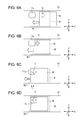
FIGS. 6A to 6D are schematic diagrams for illustrating a detection action of a position of a substrate; -
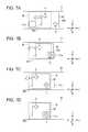
FIGS. 7A to 7D are schematic diagrams for illustrating a detection action of a substrate position according to a second embodiment of the present application; and -
FIGS. 8A to 8C are schematic diagrams for illustrating a detection action of a substrate position according to the second embodiment of the present application. - The present application will be described below in greater detail with reference to the drawings according to an embodiment.
- As described above, there are problems such as components with large heights which are mounted on a substrate being bent or removed due to the force of collision in a case where the transport of the substrate is stopped using a stopper.
- In addition, for example, in a case where a mounting action is started by a
substrate camera 17 recognizing an alignment mark D on the substrate, if the substrate bounces off the stopper and rebounds, thesubstrate camera 17 is not able to accurately recognize the alignment mark D due to the amount of the bounce back. - Furthermore, in the case of the stopper, a raising and lowering action of the stopper is necessary and excess time is taken in the positioning of the substrate to the extent of the raising and lowering action.
- The present application which is described below is able to resolve the problems above. Below, embodiments of the present application will be described while referencing the diagrams.
-
FIG. 1 is a front surface diagram illustrating in a schematic manner a component mounting device according to a first embodiment of the present application.FIG. 2 is a planar diagram of acomponent mounting device 100 which is shown inFIG. 1 , andFIG. 3 is a side surface diagram thereof - The
component mounting device 100 is provided with aframe 10, a mountinghead 30 which holds a component which is not shown and mounted the component on a circuit substrate (referred to below simply as a substrate) W which is a mounting target, a tapefeeder installation section 20 where atape feeder 90 is installed, and a transport unit 16 (refer toFIG. 2 ) which holds and transports the substrate W. - The
frame 10 has a base 11 which is provided on a bottom portion and a plurality of supportingpillars 12 which are fixed to thebase 11. In the upper portion of the plurality of supportingpillars 12, for example, twoX beams 13 which span along the X axis in the diagram are provided. For example, between the twoX beams 13, aY beam 14 spans along the Y axis and the mountinghead 30 is connected to theY beam 14. In the X beams 13 and theY beam 14, an X axis movement mechanism and a Y axis movement mechanism which are not shown are provided, and as such, it is possible for the mountinghead 30 to move along the X axis and the Y axis. The X axis movement mechanism and the Y axis movement mechanism are typically configured using a ball screw driving structure, but other structures such as a belt driving structure may be used. - A mounting
unit 40 is configured from the mountinghead 30, the X axis movement mechanism, and the Y axis movement mechanism. There are cases where a plurality of the mountingunits 40 are provided mainly in order to improve efficiency, and in this case, the plurality of mountingheads 30 are driven in the X and Y axial directions independently. - As shown in
FIG. 2 , the tapefeeder installation section 20 is disposed on both the front portion side (lower side inFIG. 2 ) and the rear portion side (upper side inFIG. 2 ) of thecomponent mounting device 100. The Y axial direction in the diagram is the front and back direction of thecomponent mounting device 100. In the tapefeeder installation section 20, a plurality of thetape feeders 90 are installed so as to line up along the X axial direction. For example, it is possible for 40 to 70 of thetape feeders 90 to be installed on the tapefeeder installation section 20. In the embodiment, it is possible for 58 of thetape feeders 90 on each of the front portion and the rear portion, a total of 116, to be installed. - Here, the tape
feeder installation section 20 is configured to be provided on both the front edge side and the rear edge side of thecomponent mounting device 100, but the tapefeeder installation section 20 may be configured to be provided on either one the front edge side or the rear edge side. - The
taper feeder 90 is formed to be long in the Y axial direction. The details of thetape feeder 90 are not shown in the diagram, but a reel is provided and carrier tape which contains an electronic component such as a condenser, a resistor, an LED, or an IC packaging is wound on the reel. In addition, thetape feeder 90 is provided with a structure for feeding out the carrier tape by step feeding and the electronic components are supplied one at a time for each of the step feeds. As shown inFIG. 2 , asupply window 91 is formed in the upper surface of the edge portion of a cassette of thetape feeder 90 and the electronic component is supplied via thesupply window 91. A region where a plurality of thesupply windows 91 are lined up, which is formed along the X axial direction due to the plurality oftape feeders 90 being lined up, is an electronic component supply region S. - Here, in the carrier tape of one of the
tape feeders 90, a plurality of the same electronic component is contained. There are cases where the same electronic component is contained over a plurality of thetape feeders 90 out of thetape feeders 90 which are mounted on the tapefeeder installation section 20. - The
transport unit 16 described above is provided in the central portion of thecomponent mounting device 100 in the Y axial direction and thetransport unit 16 transports the substrate W along the X axial direction. For example, as shown inFIG. 2 , a region on the substrate W, which is supported by thetransport unit 16 in substantially the central portion on thetransport unit 16 in the X axial direction, is a mounting region M where the mounting of the electronic component is performed due to accessing by the mountinghead 30. - As will be described later, the
component mounting device 100 detects an accurate position on the substrate W, which is transported up to the mounting region M, using thesubstrate camera 17. After the accurate position of the substrate W has been detected, the mountingunit 40 starts the electronic component mounting action. - The mounting
head 30 is provided with acarriage 31 which is connected to the Y axis movement mechanism of theY beam 14, aturret 32 which is provided so as to extend diagonally downward from thecarriage 31, and a plurality ofsuction nozzles 33 which is attached along the circumference direction of theturret 32. The suction nozzles 33 take out and hold the electronic component from the carrier tape due to a vacuum suction action. The suction nozzles 33 are able to move up and down so as to mount the electronic component on the substrate W. For example, 12 of thesuction nozzles 33 are provided. - The mounting
head 30 is able to move in the X and Y axial directions as described above, thesuction nozzles 33 move between the supply region S and the mounting region M, and in addition, moves in the X and Y axial directions in the mounting region M so as to execute the mounting in the mounting region M. - The
turret 32 is able to rotate (spin) with a shaft in a diagonal direction as the central rotation shaft. The suction nozzles 33 which are disposed so that the length direction of thesuction nozzles 33 is along the Z direction out of the plurality ofsuction nozzles 33 are thesuction nozzles 33 which are selected for mounting the electronic component on the substrate W. An arbitrary one of thesuction nozzles 33 is selected using the rotation of theturret 32. The electronic component is suctioned and held by thesuction nozzles 33 which have been selected accessing thesupply window 91 of thetape feeder 90 and the electronic components are mounted on the substrate W by being moved and lowered to the mounting region M. - The mounting
head 30 holds each of a plurality of the electronic components continuously in one process with the plurality ofsuction nozzles 33 while theturret 32 rotates. In addition, the electronic components which are suctioned by the plurality ofsuction nozzles 33 are mounted on one substrate W continuously in one process. - As shown in
FIG. 1 , thesubstrate camera 17 which detects the position of the substrate W is attached in the mountinghead 30. Thesubstrate camera 17 is able to move integrally with the mountinghead 30 using the X axis and Y axis movement mechanisms. Thesubstrate camera 17 is disposed on an upper portion of thetransport unit 16 and images an image of the substrate W from the upper portion side when the position of the substrate W is detected. As will be described later, thesubstrate camera 17 recognizes an alignment mark which is provided on the substrate W and the mountingunit 40 mounts the electronic component on the substrate W with the alignment mark as the reference position. - The
substrate camera 17 has a CCD (Charged Coupled Device), a CMOS (Complementary Metal-Oxide Semiconductor), or the like. Thesubstrate camera 17 may recognize light which has a wavelength region which is mainly visible light or may recognize light which has a wavelength range which is mainly infrared light. - The
transport unit 16 is typically a belt type of conveyer, but is not limited thereto and may be any of a roller type, a type where a support mechanism which supports the substrate W moves by sliding, a non-contact type, or the like. The transport unit has aguide rail 16 a which is provided along the X axial direction. Due to this, there is transportation with deviation in the Y axial direction of the substrate W which is transported being regulated. -
FIG. 4 is a block diagram illustrating a configuration of a control system of thecomponent mounting device 100. - The control system has a main controller 21 (or a host computer). In the
main controller 21, thetape feeder 90, thesubstrate camera 17, thetransport unit 16, the mountingunit 40, aninput section 18, and adisplay section 19 are electrically connected. - The
tape feeder 90 has a built-in memory which is not shown. The built-in memory is electrically connected to themain controller 21 by thetape feeder 90 being set in the tapefeeder installation section 20. In the built-in memory, information on the electronic component which is contained in thetape feeder 90 is stored in advance. Due to this, themain controller 21 recognizes which of thetape feeders 90 which has which type of electronic component is set in which position in the tapefeeder installation section 20. The information on the electronic component is information such as the type of the electronic component or the number of the electronic components which thetape feeder 90 has. - Alternatively, the information on which of the
tape feeders 90 which has which type of the electronic component is set in which position in the tapefeeder installation section 20 may be input into themain controller 21 via theinput section 18 manually by an operator. - In each of the movement mechanisms and the mounting
head 30 of the mountingunit 40, motors (not shown) which are installed therein and drivers which drive each of the motors are provided. The drivers drive each of the movement mechanisms and the mountinghead 30 according to control signals due to themain controller 21 outputting the control signals to the drivers. - The
input section 18 is a device which, for example, is operated by the operator for the operator to input information which is necessary for the mounting process such as the type of the substrate W which is the mounting target to themain controller 21. Thedisplay section 19 is a device which, for example, displays information which is input via theinput section 18 by the operator, information which other information which is necessary. - The
main controller 21 has, for example, a function of a computer such as a CPU, a RAM, and a ROM and functions as a control unit. Themain controller 21 may be realized by a device such as a PLD (Programmable Logic Device) such as a FPGA (Field Programmable Gate Array) or another ASIC (Application Specific Integrated Circuit). -
FIG. 5 is a flowchart illustrating mainly a process of themain controller 21 when the position of the substrate W is detected.FIGS. 6A to 6D are schematic diagrams for describing a detection action of the position of the substrate W. - Before the
component mounting device 100 starts the mounting process, the operator inputs information which is necessary for the mounting process, for example, information on the type of substrate and the like, to themain controller 21 via theinput section 18. - As one example, the
substrate camera 17 waits at the downstream side of the substrate W in the transport direction (the direction from the right side to the left side inFIGS. 6A to 6D ) and is stationary at a position so that animaging range 17 a (the detection region) overlaps with the mounting position M. In addition, thesubstrate camera 17 matches in practice a position in a direction which intersects with the transport direction (the Y axial direction) with a position in the Y axial direction which is the alignment mark D which is a second detection target provided on the substrate W which is the mounting target. Typically, the Y coordinate of the central position of theimaging range 17 a is matched in practice with the Y coordinate of the alignment mark D. The alignment mark D is provided in the downstream edge portion W1 which is a first detection target so as to be separated by a predetermined distance from the downstream edge portion W1 at least in the transportation direction. - The
main controller 21 has the information on the type of substrate as described above. Accordingly, it is sufficient if thesubstrate camera 17 stores the position (here, the position of the Y coordinate) of the alignment mark D which the substrate W which is the mounting target has and waits at the position in the Y axial direction according to the position of the alignment mark. - Here, the
transport unit 16 is set so that deviation in the position of the substrate W in the Y direction is not generated in practice using theguide rail 16 a as described above. Accordingly, it is sufficient if thesubstrate camera 17 waits at the position of the Y coordinate which has been determined in advance (according to the position of the alignment mark D). - As shown in
FIG. 6A , the substrate W is transported into the component mounting device 100 (step 101). Then, as shown inFIG. 6B , thesubstrate camera 17 detects the downstream edge portion W1 which is the first detection target of the substrate W (step 102). Here, the substrate W is recognized using an existing image processing technique. For example, it is possible to recognize the substrate W using the difference in the brightness of the substrate W and the brightness of the background at the downstream side in the Z axial direction due to the substrate W. - When the downstream edge section W1 of the substrate W is detected by the
substrate camera 17, themain controller 21 outputs the stop signal for stopping the transporting of the substrate W to the transport unit 16 (step 103). At this time, themain controller 21 at least has the function as an output section of an information processing device. - The
transport unit 16 receives the stop signal and actually stops the substrate W by stopping the transporting thereof As shown inFIG. 6B , since there is a time lag from the detection of the downstream edge portion W1 of the substrate W by thesubstrate camera 17 until the substrate W actually is stopped, the substrate W moves a predetermined distance in the time lag as shown IFIG. 6C . Alternatively, even if the time lag is sufficiently short, there may be a slip due to the inertia of the substrate W on the transport belt. Below, the distance which the substrate W moves in the time lag and the like is referred to as a surplus movement distance L. - The surplus movement distance L is set so as to be within the
imaging range 17 a of thesubstrate camera 17 in advance. The size of theimaging range 17 a is, for example, 4 mm×4 mm, but is not limited thereto. - The
main controller 21 calculates the coordinate (here, X coordinate) of the downstream edge portion W1 based on the image information of the downstream edge portion W1 of the substrate W when the substrate W has actually stopped which is acquired via the substrate camera 17 (step 104). - The
main controller 21 calculates the position of the alignment mark D based on the coordinates of the downstream edge portion W1 (step 105). The alignment mark D is provided in a predetermined position on the substrate according to, for example, the type of substrate. Since themain controller 21 acquires the information on the type of substrate at the start, there is information on the coordinates of the alignment mark D in the substrate W which is included in the information on the type of substrate. Accordingly, themain controller 21 is able to calculate the coordinates of the alignment mark D which is a position which is separated from the downstream edge portion W1 by the predetermined distance. - When the
main controller 21 calculates the alignment mark D, thesubstrate camera 17 is moved so that the alignment mark D enters theimaging range 17 a as shown inFIG. 6D . Typically, thesubstrate camera 17 is moved so that the central position of the alignment mark D matches with the central position of theimaging range 17 a. Due to this, thesubstrate camera 17 recognizes the alignment mark D (step 106). Then, instep 107, themain controller 21 starts the mounting action using the mountinghead 30 with the coordinates of the alignment mark D as the reference. - Here, in
FIG. 6C , a portion of the alignment mark D enters theimaging range 17 a when the substrate W moves the surplus movement distance L and is stopped. This is because the size of theimaging range 17 a and the alignment mark D are schematically shown to be large with regard to the size of the substrate W. Accordingly, naturally, there are cases where the alignment mark D does not enter theimaging range 17 a when the substrate W is stopped. - The shape of the alignment mark is a cross shape in
FIGS. 6A to 6D , but may be any of a circle, a square, a star shape, or the like. - As described above, in the embodiment, the alignment mark D of the substrate W, where the stop signal is output, and after that, the transporting of the substrate W has been actually stopped when the downstream edge portion W1 of the substrate W has been detected (based on the detection), is detected. Accordingly, it is possible to easily detect the alignment mark D for the mounting
head 30 to start the mounting action. That is, it is possible for the stop position of the substrate W to be accurately detected and it is possible for thesubstrate camera 17 to be moved to an appropriate position where the alignment mark D enters theimaging range 17 a. - Being based on the detection of the downstream edge portion W1 of the substrate W is not limited to the “instant” that the downstream edge portion W1 is detected. The meaning of “based” includes the concept where there is a time lag until the stop signal is output with the detection of the downstream edge portion W1 as a trigger.
- In the embodiment, the
substrate camera 17 is used in the detection of the downstream edge portion W1. In particular, by the downstream edge portion W1 of the substrate W from the start of deceleration to stopping entering theimaging range 17 a of thesubstrate camera 17, both the timing of the output of the stop signal of the substrate W and the position of the downstream edge portion W1 which has been actually stopped are able to be recognized using thesubstrate camera 17. It is possible for the alignment mark D which is separated from the downstream edge portion W1 to be easily detected if the position of the downstream edge portion W1 of the substrate W which is actually stopped is recognized. - In the embodiment, since the downstream edge portion W1 of the substrate W is detected, the detection is easy compared to the case where, for example, a mark or the like which is attached to the substrate W is detected.
-
FIGS. 7A to 7D are schematic diagrams for describing the detection action of the substrate position according to a second embodiment of the present application. In the description from here, the description of the members and functions which are included in thecomponent mounting device 100 according to the embodiment above and the similarities with regard to the actions and the like which are shown inFIGS. 5 to 6D is simplified or omitted and the points which differ are the focus of the description. - The shape of a downstream edge portion W2 of a substrate W′ according to the embodiment is different to the shape of the edge portion of the normal substrate W (refer to
FIG. 6 ) and is a concave shape (notch shape) and an upstream edge portion W3 is a linear shape in the same manner as the normal substrate. That is, the substrate W′ is a so-called abnormal substrate. - In a case where the substrate W′ is transported, as shown in
FIG. 7A , thesubstrate camera 17 waits by being positioned in front (at a lower side inFIG. 7A ) in the Y axial direction on thetransport unit 16. In the substrate W′, the alignment mark D which is provided in the vicinity of the downstream edge portion W2 and the alignment mark D which is provided in the vicinity of the upstream edge portion W3 are coordinates which are different in the Y axial direction. In the example, thesubstrate camera 17 detects the alignment mark D which is provided in the vicinity of the upstream edge portion W3. Here, there are cases where the normal substrate W shown inFIGS. 6A to 6D also has two alignment marks D as in the substrate W′. - As shown in
FIG. 7B , the downstream edge portion W2 of the substrate W′ passes too far past theimaging range 17 a of thesubstrate camera 17. When the upstream edge portion W3 of the substrate W′ enters theimaging range 17 a, themain controller 21 outputs the stop signal to thetransport unit 16. - As shown in
FIG. 7C , the substrate W′ moves the surplus movement distance and is stopped. Themain controller 21 recognizes the coordinates (here, the X coordinates) of the upstream edge portion W3 of the substrate W′ which has been stopped. - The
main controller 21 calculates the coordinates of the upstream edge portion W3 and the position of the alignment mark D on the upstream based on the information on the substrate and moves thesubstrate camera 17 to the coordinates of the alignment mark D as shown inFIG. 7D . Then, the mountinghead 30 starts the mounting action with the position of the alignment mark D as the reference. - In the embodiment such as this, it is possible for the
main controller 21 to select the upstream edge portion W3, which is where the detection using thesubstrate camera 17 is easier out of the edge portions, as the detection target in a case where the shape of the downstream edge portion W2 of the substrate is different from normal. - In the embodiment, the substrate which has a shape where the shape of the downstream edge portion W1 is a shape which is different from normal is used as the substrate which is the mounting target. However, a substrate where the shape of the upstream edge portion is a shape which is different from normal may be used as the substrate which is the mounting target. In this case, the
main controller 21 detects the downstream edge portion W1 and detects the alignment mark D based on the detection as in the first embodiment described above. - As the abnormal substrate, other than the substrate where the edge portion is concave, there are cases where there is a substrate where the edge portion is convex, diagonal, curved or a shape which is a combination of these.
-
FIGS. 8A to 8C are schematic diagrams for describing the detection action of the substrate position according to the second embodiment of the present application. - As shown in
FIG. 8A , the substrate W is transported. Theimaging range 17 a which is the detection region of thesubstrate camera 17 is disposed further to the downstream side than the substrate W. - As shown in
FIG. 8B , themain controller 21 outputs the stop signal based on the detection of the downstream edge portion W1 of the substrate W in theimaging range 17 a. At this time, themain controller 21 outputs the stop signal at a timing where the alignment mark D on the substrate W which is transported is stopped in theimaging range 17 a. By themain controller 21 storing the information which is related to the information on the substrate W and the surplus distance information L described above, it is possible for the action such as this to be realized. Due to this, as shown inFIG. 8C , the output timing of the stop signal is slightly delayed and the alignment mark D enters theimaging range 17 a at a timing when the substrate W is actually stopped. - In this manner, the embodiment uses the generation of the time lag from the output of the stop signal due to the detection of the downstream edge portion W1 until the substrate W which is transported is actually stopped. It is possible to easily detect the alignment mark D by outputting the stop signal at a timing when the alignment mark D of the substrate W is stopped in the
imaging range 17 a of thesubstrate camera 17. - The present application is not limited to the embodiments described above and other various embodiments are able to be realized.
- In the embodiment described above, there is an example where the
substrate camera 17 is the detection unit. However, a sensor other than a camera, for example, a line sensor, may be used as the unit which detects the first detection target (for example, the substrate edge portion). It is possible to use, for example, a light sensor as the line sensor. A first sensor which is a line sensor detects the downstream edge portion W1 of the substrate W, themain controller 21 outputs the stop signal, and furthermore, a second sensor detects the downstream edge portion W1 of the substrate W which has actually stopped. Then, themain controller 21 calculates the position of the alignment mark D based on the position of the downstream edge portion W1 and the second sensor described above or another third sensor detects the alignment mark D. The second sensor described above may be a line sensor or may be a camera sensor. A camera is used as the third sensor. - By using a portion out of a plurality of lines along the X axial direction for each pixel in the
substrate camera 17, thesubstrate camera 17 may be used as a sensor which is close to the line sensor. - The
substrate camera 17 may not be provided so as to be integral with the mountinghead 30. That is, there may be a form where the movement of thesubstrate camera 17 and the mountinghead 30 are individually independent. This is the same as the case where a line sensor or another sensor is used instead of thesubstrate camera 17. - The
main controller 21 may control the transport speed of the substrate using thetransport unit 16 based on the coordinates of the edge portion of the substrate which has been detected when the substrate stops. For example, in a case where the edge portion of the substrate which has actually stopped is excluded from theimaging range 17 a or is in a state which is close to being excluded, themain controller 21 is able to set the transport speed of the substrate which is the next mounting target to be lower to the extent of a predetermined speed. Due to this, it is possible for the transport speed of the substrate due to thetransport unit 16 to be an appropriate speed which matches the detection capability of thesubstrate camera 17. - In the description above, the
main controller 21 before the mounting process stores various pieces of information on the substrate which is the mounting target. However, for example, when a second substrate, which is the next mounting target of a first substrate which is the mounting target, is waiting at the upstream side of the mounting region M, the type of the substrate (shape and the like) of the second substrate may be identified using a sensor such as a camera. - In the embodiment described above, the
substrate camera 17 detects the edge portion of the substrate as the first detection target for outputting the stop signal of the substrate. However, the first detection target may not be the edge portion and may be a mark which is provided at a position which is different to the alignment mark D in the transport direction and which is able to be recognized by the substrate camera 17 (or another sensor described above). The mark is, for example, a perforation, a guide line, or another mark which is able to be identified. - The mounting
head 30 is provided with theturret 32 which rotates and the plurality ofsuction nozzles 33. However, the mounting head may have only one suction nozzle. Alternatively, the mounting head may not have the turret which rotates and may be a linear type where a plurality of suction nozzles which are lined up in a linear manner. - Out of the characteristic sections of each of the embodiments which are described above, it is possible for at least two of the characteristic sections to be combined.
- It is possible for the present application to be configured as below.
-
- (1) A component mounting device which is provided with a transport unit which transports a substrate, a mounting unit which mounts a component on the substrate, a detection unit which is able to detect a first detection target which is provided on the substrate and a second detection target which is provided to be separated by a predetermined distance from the first detection target on the substrate at least in the transportation direction and is a reference position of a mounting action by the mounting unit, and a control unit which outputs a stop signal for stopping the transport of the substrate to the transport unit and detects the second detection target of the substrate which has been stopped using the detection unit based on the detection of the first detection target by the detection unit.
- (2) The component mounting device described in (1) where the detection unit has a camera, and the control unit outputs the stop signal so that the substrate is stopped within an imaging range of the camera and the position of the second detection target is calculated based on the position of the first detection target on the substrate which has stopped.
- (3) The component mounting device described in (1) or (2) where the detection unit detects an edge portion of the substrate in the transport direction as the first detection target.
- (4) The component mounting device described in one out of any of (1) to (3) where the control unit detects one of either out of the edge portion on the downstream side or the edge portion on the upstream side with regard to the substrate in the transport direction based on the information on the shape of the edge portions of the substrate in the transport direction.
- (5) The component mounting device described in (1) where the detection unit has a detection region which is disposed further downstream than the substrate which is transported at a point in time when the control unit outputs the stop signal, and the control unit outputs the stop signal at a timing so that the second detection target on the substrate which is transported stops within the detection region of the detection unit.
- (6) The component mounting device described in (5) where the detection unit detects the edge portion of the substrate on the downstream side in the transport direction as the first detection target.
- (7) The component mounting device described in one out of any of (1) to (6) where the mounting unit has a head which holds the component and a movement mechanism which moves the head, and the detection unit is provided so as to be able to move integrally with the head using the movement mechanism.
- (8) The component mounting device described in one out of any of (1) to (7) where the control unit controls the transport speed of the substrate using the transport unit based on information on the position of the first detection target which has been detected when the substrate has stopped.
- (9) The component mounting device described in (1) or (5) where the detection unit is a camera.
- (10) An information processing device which uses a component mounting device, which is provided with a transport unit which transports a substrate, a mounting unit which mounts a component on the substrate, and a detection unit which is able to detect a first detection target which is provided on the substrate and a second detection target which is provided to be separated by a predetermined distance from the first detection target on the substrate at least in the transportation direction and is a reference position of a mounting action by the mounting unit, which is provided with an output section which outputs a stop signal for stopping transport of a substrate to the transport unit based on detection of the first detection target by the detection unit, and a detection control section which detects a second detection target on the substrate which has stopped using the detection unit.
- (11) A position detection method which includes transporting of a substrate which is a component mounting target using a transport unit, detecting a first detection target which is provided on the substrate which is transported using a detection unit, outputting a stop signal for stopping the transporting of the substrate to the transport unit based on detection of the first detection target using the detection unit, and detecting a second detection target, which is provided on the substrate which has stopped, is provided to be separated by a predetermined distance from the first detection target on the substrate at least in the transportation direction, and is a reference position in a component mounting action, using a detection unit.
- (12) A substrate manufacturing method which includes transporting of a substrate which is a component mounting target using a transport unit, detecting a first detection target which is provided on the substrate which is transported using a detection unit, outputting a stop signal for stopping the transporting of the substrate to the transport unit based on detection of the first detection target using the detection unit, detecting second detection target, which is provided on the substrate which has stopped and is provided to be separated by a predetermined distance from the first detection target on the substrate at least in the transportation direction, using a detection unit, and mounting the component on the substrate with the second detection target which has been detected as a reference position.
- It should be understood that various changes and modifications to the presently preferred embodiments described herein will be apparent to those skilled in the art. Such changes and modifications can be made without departing from the spirit and scope of the present subject matter and without diminishing its intended advantages. It is therefore intended that such changes and modifications be covered by the appended claims.
Claims (12)
1. A component mounting device comprising:
a transport unit which transports a substrate;
a mounting unit which mounts a component on the substrate;
a detection unit which is able to detect a first detection target which is provided on the substrate and a second detection target which is provided to be separated by a predetermined distance from the first detection target on the substrate at least in the transportation direction and is a reference position of a mounting action by the mounting unit; and
a control unit which outputs a stop signal for stopping the transport of the substrate to the transport unit and detects the second detection target of the substrate which has been stopped using the detection unit based on the detection of the first detection target by the detection unit.
2. The component mounting device according to claim 1 ,
wherein the detection unit has a camera, and
the control unit outputs the stop signal so that the substrate is stopped within an imaging range of the camera and the position of the second detection target is calculated based on the position of the first detection target on the substrate which has stopped.
3. The component mounting device according to claim 1 ,
wherein the detection unit detects an edge portion of the substrate in the transport direction as the first detection target.
4. The component mounting device according to claim 1 ,
wherein the control unit detects one of either out of the edge portion on the downstream side or the edge portion on the upstream side with regard to the substrate in the transport direction based on the information on the shape of the edge portions of the substrate in the transport direction.
5. The component mounting device according to claim 1 ,
wherein the detection unit has a detection region which is disposed further downstream than the substrate which is transported at a point in time when the control unit outputs the stop signal, and
the control unit outputs the stop signal at a timing so that the second detection target on the substrate which is transported stops within the detection region of the detection unit.
6. The component mounting device according to claim 5 ,
wherein the detection unit detects the edge portion of the substrate on the downstream side in the transport direction as the first detection target.
7. The component mounting device according to claim 1 ,
wherein the mounting unit has a head which holds the component and a movement mechanism which moves the head, and
the detection unit is provided so as to be able to move integrally with the head using the movement mechanism.
8. The component mounting device according to claim 1 ,
wherein the control unit controls the transport speed of the substrate using the transport unit based on information on the position of the first detection target which has been detected when the substrate has stopped.
9. The component mounting device according to claim 1 ,
wherein the detection unit is a camera.
10. An information processing device which uses a component mounting device, which is provided with a transport unit which transports a substrate, a mounting unit which mounts a component on the substrate, and a detection unit which is able to detect a first detection target which is provided on the substrate and a second detection target which is provided to be separated by a predetermined distance from the first detection target on the substrate at least in the transportation direction and is a reference position of a mounting action by the mounting unit, comprising:
an output section which outputs a stop signal for stopping transport of a substrate to the transport unit based on detection of the first detection target by the detection unit; and
a detection control section which detects a second detection target on the substrate which has stopped using the detection unit.
11. A position detection method comprising:
transporting of a substrate which is a component mounting target using a transport unit;
detecting a first detection target which is provided on the substrate which is transported using a detection unit;
outputting a stop signal for stopping the transporting of the substrate to the transport unit based on detection of the first detection target using the detection unit; and
detecting a second detection target, which is provided on the substrate which has stopped, is provided to be separated by a predetermined distance from the first detection target on the substrate at least in the transportation direction, and is a reference position in a component mounting action, using a detection unit.
12. A substrate manufacturing method comprising:
transporting of a substrate which is a component mounting target using a transport unit;
detecting a first detection target which is provided on the substrate which is transported using a detection unit;
outputting a stop signal for stopping the transporting of the substrate to the transport unit based on detection of the first detection target using the detection unit;
detecting second detection target, which is provided on the substrate which has stopped and is provided to be separated by a predetermined distance from the first detection target on the substrate at least in the transportation direction, using a detection unit; and
mounting the component on the substrate with the second detection target which has been detected as a reference position.
Applications Claiming Priority (2)
| Application Number | Priority Date | Filing Date | Title |
|---|---|---|---|
| JP2011078448A JP5721072B2 (en) | 2011-03-31 | 2011-03-31 | Component mounting apparatus, information processing apparatus, position detection method, and board manufacturing method |
| JP2011-078448 | 2011-03-31 |
Publications (1)
| Publication Number | Publication Date |
|---|---|
| US20120249772A1 true US20120249772A1 (en) | 2012-10-04 |
Family
ID=46926725
Family Applications (1)
| Application Number | Title | Priority Date | Filing Date |
|---|---|---|---|
| US13/413,382 Abandoned US20120249772A1 (en) | 2011-03-31 | 2012-03-06 | Component mounting device, information processing device, position detection method, and substrate manufacturing method |
Country Status (3)
| Country | Link |
|---|---|
| US (1) | US20120249772A1 (en) |
| JP (1) | JP5721072B2 (en) |
| CN (1) | CN102740674B (en) |
Cited By (4)
| Publication number | Priority date | Publication date | Assignee | Title |
|---|---|---|---|---|
| US20120246929A1 (en) * | 2011-03-31 | 2012-10-04 | Sony Corporation | Component mounting device and substrate manufacturing method |
| EP2988583A4 (en) * | 2014-06-20 | 2016-05-18 | Yamaha Motor Co Ltd | Substrate working device, substrate working method, and substrate working system |
| EP3579676A4 (en) * | 2017-01-31 | 2020-01-22 | Fuji Corporation | Coordinate data generation device and coordinate data generation method |
| US11385619B2 (en) * | 2017-03-23 | 2022-07-12 | Fuji Corporation | Mounting system and display control device |
Families Citing this family (11)
| Publication number | Priority date | Publication date | Assignee | Title |
|---|---|---|---|---|
| JP6164863B2 (en) * | 2013-02-18 | 2017-07-19 | Juki株式会社 | Electronic component mounting system and board conveying method of electronic component mounting system |
| WO2014136211A1 (en) * | 2013-03-05 | 2014-09-12 | 富士機械製造株式会社 | Component-mounting machine |
| JP6253177B2 (en) * | 2013-05-13 | 2017-12-27 | Jukiオートメーションシステムズ株式会社 | POSITION DETECTION DEVICE, POSITION DETECTION METHOD, PROGRAM, AND BOARD MANUFACTURING METHOD |
| JP6130240B2 (en) * | 2013-06-21 | 2017-05-17 | 富士機械製造株式会社 | Substrate conveyor control system and substrate work machine using the same |
| JP6198312B2 (en) * | 2013-09-30 | 2017-09-20 | Jukiオートメーションシステムズ株式会社 | Three-dimensional measuring apparatus, three-dimensional measuring method, and substrate manufacturing method |
| JP6645007B2 (en) * | 2014-11-25 | 2020-02-12 | 日本電気株式会社 | Board identification apparatus, board identification method, and board traceability system |
| KR102436258B1 (en) * | 2015-05-04 | 2022-08-26 | 삼성디스플레이 주식회사 | Lamination device of display device and method for detecting align mark |
| JP6528133B2 (en) * | 2016-03-04 | 2019-06-12 | パナソニックIpマネジメント株式会社 | Component mounting device |
| WO2018134892A1 (en) * | 2017-01-17 | 2018-07-26 | 株式会社Fuji | Component mounter |
| JP2018189387A (en) * | 2017-04-28 | 2018-11-29 | セイコーエプソン株式会社 | Electronic component conveyance device and electronic component inspection device |
| JP6843709B2 (en) * | 2017-07-04 | 2021-03-17 | ヤマハ発動機株式会社 | Board work equipment |
Citations (6)
| Publication number | Priority date | Publication date | Assignee | Title |
|---|---|---|---|---|
| US4810154A (en) * | 1988-02-23 | 1989-03-07 | Molex Incorporated | Component feeder apparatus and method for vision-controlled robotic placement system |
| US6195454B1 (en) * | 1995-11-15 | 2001-02-27 | Kabushiki Kaisha Sankyo Seiki Seisakusho | Component mounting apparatus |
| US20050077340A1 (en) * | 2001-03-06 | 2005-04-14 | Matsushita Electric Industrial Co., Ltd. | Method, apparatus, system, method and device for data creating, and program for mounting electronic component |
| US20050115060A1 (en) * | 2002-04-01 | 2005-06-02 | Toshihiro Kondo | Working system for substrate |
| US20080014772A1 (en) * | 2006-07-14 | 2008-01-17 | Juki Corporation | Component mounting position correcting method and component mouting apparatus |
| US8215891B2 (en) * | 2007-12-20 | 2012-07-10 | Dainippon Screen Mfg. Co., Ltd. | Substrate treating apparatus, and a substrate transporting method therefor |
Family Cites Families (5)
| Publication number | Priority date | Publication date | Assignee | Title |
|---|---|---|---|---|
| JP3231344B2 (en) * | 1991-02-14 | 2001-11-19 | 松下電器産業株式会社 | Substrate positioning device |
| JP2003110286A (en) * | 2001-09-28 | 2003-04-11 | Matsushita Electric Ind Co Ltd | Mounting machine |
| JP2004228326A (en) * | 2003-01-22 | 2004-08-12 | Fuji Mach Mfg Co Ltd | Method and device for controlling substrate stop position |
| DE602004011752T2 (en) * | 2004-03-25 | 2009-02-05 | Hitachi High-Tech Instruments Co., Ltd. | Electronic component feed device and device for mounting electronic components with an electronic component feed device |
| JP4788362B2 (en) * | 2006-02-03 | 2011-10-05 | パナソニック株式会社 | Substrate alignment method |
-
2011
- 2011-03-31 JP JP2011078448A patent/JP5721072B2/en active Active
-
2012
- 2012-03-06 US US13/413,382 patent/US20120249772A1/en not_active Abandoned
- 2012-03-23 CN CN201210080976.5A patent/CN102740674B/en active Active
Patent Citations (6)
| Publication number | Priority date | Publication date | Assignee | Title |
|---|---|---|---|---|
| US4810154A (en) * | 1988-02-23 | 1989-03-07 | Molex Incorporated | Component feeder apparatus and method for vision-controlled robotic placement system |
| US6195454B1 (en) * | 1995-11-15 | 2001-02-27 | Kabushiki Kaisha Sankyo Seiki Seisakusho | Component mounting apparatus |
| US20050077340A1 (en) * | 2001-03-06 | 2005-04-14 | Matsushita Electric Industrial Co., Ltd. | Method, apparatus, system, method and device for data creating, and program for mounting electronic component |
| US20050115060A1 (en) * | 2002-04-01 | 2005-06-02 | Toshihiro Kondo | Working system for substrate |
| US20080014772A1 (en) * | 2006-07-14 | 2008-01-17 | Juki Corporation | Component mounting position correcting method and component mouting apparatus |
| US8215891B2 (en) * | 2007-12-20 | 2012-07-10 | Dainippon Screen Mfg. Co., Ltd. | Substrate treating apparatus, and a substrate transporting method therefor |
Cited By (5)
| Publication number | Priority date | Publication date | Assignee | Title |
|---|---|---|---|---|
| US20120246929A1 (en) * | 2011-03-31 | 2012-10-04 | Sony Corporation | Component mounting device and substrate manufacturing method |
| US8720045B2 (en) * | 2011-03-31 | 2014-05-13 | Sony Corporation | Apparatus for mounting components on a substrate |
| EP2988583A4 (en) * | 2014-06-20 | 2016-05-18 | Yamaha Motor Co Ltd | Substrate working device, substrate working method, and substrate working system |
| EP3579676A4 (en) * | 2017-01-31 | 2020-01-22 | Fuji Corporation | Coordinate data generation device and coordinate data generation method |
| US11385619B2 (en) * | 2017-03-23 | 2022-07-12 | Fuji Corporation | Mounting system and display control device |
Also Published As
| Publication number | Publication date |
|---|---|
| JP2012212817A (en) | 2012-11-01 |
| JP5721072B2 (en) | 2015-05-20 |
| CN102740674B (en) | 2017-03-01 |
| CN102740674A (en) | 2012-10-17 |
Similar Documents
| Publication | Publication Date | Title |
|---|---|---|
| US20120249772A1 (en) | Component mounting device, information processing device, position detection method, and substrate manufacturing method | |
| JP5881244B2 (en) | Component mounting apparatus, board detection method, and board manufacturing method | |
| US20120253499A1 (en) | Component mounting device, information processing device, information processing method, and substrate manufacturing method | |
| JP4809799B2 (en) | Mounting machine, mounting method thereof, and moving method of board imaging means in mounting machine | |
| JP5139569B1 (en) | Substrate transfer device, substrate transfer method, and surface mounter | |
| US11357148B2 (en) | Component mounting device | |
| KR20160118906A (en) | An apparatus for supplying component | |
| JP5574690B2 (en) | Component mounting apparatus and component mounting method | |
| US10842060B2 (en) | Component mounting device | |
| US20130074329A1 (en) | Mounting apparatus, electronic component mounting method, substrate production method, and program | |
| US10674650B2 (en) | Component mounting device | |
| JP2005072046A (en) | Apparatus for packaging electronic component | |
| JP6621991B2 (en) | Electronic component supply device and electronic component mounting device | |
| WO2018158888A1 (en) | Backup-pin recognizing method and component mounting device | |
| US8720045B2 (en) | Apparatus for mounting components on a substrate | |
| US20130110277A1 (en) | Component mounting apparatus, information processing apparatus, information processing method, and production method for a substrate | |
| JP5041878B2 (en) | Component recognition device, surface mounter, and component testing device | |
| US10798858B2 (en) | Component mounting device and method for capturing image of nozzle a component mounting device | |
| JP2013179115A (en) | Component mounting device and manufacturing method of substrate | |
| JP5977579B2 (en) | Board work equipment | |
| JP6093214B2 (en) | Component mounting equipment | |
| US20180352691A1 (en) | Component mounting machine | |
| JP2012160525A (en) | Electronic component mounting device and electronic component mounting method | |
| JPH10135693A (en) | Inspection device for electronic parts | |
| US10561051B2 (en) | Movement error detection apparatus of mounting head, and component mounting apparatus |
Legal Events
| Date | Code | Title | Description |
|---|---|---|---|
| AS | Assignment |
Owner name: SONY CORPORATION, JAPAN Free format text: ASSIGNMENT OF ASSIGNORS INTEREST;ASSIGNOR:NAKAMURA, TAKESHI;REEL/FRAME:027822/0602 Effective date: 20120229 |
|
| STCB | Information on status: application discontinuation |
Free format text: ABANDONED -- FAILURE TO RESPOND TO AN OFFICE ACTION |