US20120119384A1 - Semiconductor device and manufacturing method thereof - Google Patents
Semiconductor device and manufacturing method thereof Download PDFInfo
- Publication number
- US20120119384A1 US20120119384A1 US13/387,204 US201113387204A US2012119384A1 US 20120119384 A1 US20120119384 A1 US 20120119384A1 US 201113387204 A US201113387204 A US 201113387204A US 2012119384 A1 US2012119384 A1 US 2012119384A1
- Authority
- US
- United States
- Prior art keywords
- semiconductor substrate
- hole
- layer
- semiconductor device
- forming
- Prior art date
- Legal status (The legal status is an assumption and is not a legal conclusion. Google has not performed a legal analysis and makes no representation as to the accuracy of the status listed.)
- Abandoned
Links
Images


Classifications
-
- H—ELECTRICITY
- H01—ELECTRIC ELEMENTS
- H01L—SEMICONDUCTOR DEVICES NOT COVERED BY CLASS H10
- H01L21/00—Processes or apparatus adapted for the manufacture or treatment of semiconductor or solid state devices or of parts thereof
- H01L21/70—Manufacture or treatment of devices consisting of a plurality of solid state components formed in or on a common substrate or of parts thereof; Manufacture of integrated circuit devices or of parts thereof
- H01L21/71—Manufacture of specific parts of devices defined in group H01L21/70
- H01L21/768—Applying interconnections to be used for carrying current between separate components within a device comprising conductors and dielectrics
- H01L21/76898—Applying interconnections to be used for carrying current between separate components within a device comprising conductors and dielectrics formed through a semiconductor substrate
-
- H—ELECTRICITY
- H01—ELECTRIC ELEMENTS
- H01L—SEMICONDUCTOR DEVICES NOT COVERED BY CLASS H10
- H01L23/00—Details of semiconductor or other solid state devices
- H01L23/48—Arrangements for conducting electric current to or from the solid state body in operation, e.g. leads, terminal arrangements ; Selection of materials therefor
- H01L23/481—Internal lead connections, e.g. via connections, feedthrough structures
-
- H—ELECTRICITY
- H01—ELECTRIC ELEMENTS
- H01L—SEMICONDUCTOR DEVICES NOT COVERED BY CLASS H10
- H01L24/00—Arrangements for connecting or disconnecting semiconductor or solid-state bodies; Methods or apparatus related thereto
- H01L24/01—Means for bonding being attached to, or being formed on, the surface to be connected, e.g. chip-to-package, die-attach, "first-level" interconnects; Manufacturing methods related thereto
- H01L24/02—Bonding areas ; Manufacturing methods related thereto
- H01L24/03—Manufacturing methods
-
- H—ELECTRICITY
- H01—ELECTRIC ELEMENTS
- H01L—SEMICONDUCTOR DEVICES NOT COVERED BY CLASS H10
- H01L24/00—Arrangements for connecting or disconnecting semiconductor or solid-state bodies; Methods or apparatus related thereto
- H01L24/01—Means for bonding being attached to, or being formed on, the surface to be connected, e.g. chip-to-package, die-attach, "first-level" interconnects; Manufacturing methods related thereto
- H01L24/02—Bonding areas ; Manufacturing methods related thereto
- H01L24/04—Structure, shape, material or disposition of the bonding areas prior to the connecting process
- H01L24/05—Structure, shape, material or disposition of the bonding areas prior to the connecting process of an individual bonding area
-
- H—ELECTRICITY
- H01—ELECTRIC ELEMENTS
- H01L—SEMICONDUCTOR DEVICES NOT COVERED BY CLASS H10
- H01L2224/00—Indexing scheme for arrangements for connecting or disconnecting semiconductor or solid-state bodies and methods related thereto as covered by H01L24/00
- H01L2224/01—Means for bonding being attached to, or being formed on, the surface to be connected, e.g. chip-to-package, die-attach, "first-level" interconnects; Manufacturing methods related thereto
- H01L2224/02—Bonding areas; Manufacturing methods related thereto
- H01L2224/023—Redistribution layers [RDL] for bonding areas
- H01L2224/0237—Disposition of the redistribution layers
- H01L2224/02372—Disposition of the redistribution layers connecting to a via connection in the semiconductor or solid-state body
-
- H—ELECTRICITY
- H01—ELECTRIC ELEMENTS
- H01L—SEMICONDUCTOR DEVICES NOT COVERED BY CLASS H10
- H01L2224/00—Indexing scheme for arrangements for connecting or disconnecting semiconductor or solid-state bodies and methods related thereto as covered by H01L24/00
- H01L2224/01—Means for bonding being attached to, or being formed on, the surface to be connected, e.g. chip-to-package, die-attach, "first-level" interconnects; Manufacturing methods related thereto
- H01L2224/02—Bonding areas; Manufacturing methods related thereto
- H01L2224/023—Redistribution layers [RDL] for bonding areas
- H01L2224/0237—Disposition of the redistribution layers
- H01L2224/02375—Top view
-
- H—ELECTRICITY
- H01—ELECTRIC ELEMENTS
- H01L—SEMICONDUCTOR DEVICES NOT COVERED BY CLASS H10
- H01L2224/00—Indexing scheme for arrangements for connecting or disconnecting semiconductor or solid-state bodies and methods related thereto as covered by H01L24/00
- H01L2224/01—Means for bonding being attached to, or being formed on, the surface to be connected, e.g. chip-to-package, die-attach, "first-level" interconnects; Manufacturing methods related thereto
- H01L2224/02—Bonding areas; Manufacturing methods related thereto
- H01L2224/023—Redistribution layers [RDL] for bonding areas
- H01L2224/0237—Disposition of the redistribution layers
- H01L2224/02381—Side view
-
- H—ELECTRICITY
- H01—ELECTRIC ELEMENTS
- H01L—SEMICONDUCTOR DEVICES NOT COVERED BY CLASS H10
- H01L2224/00—Indexing scheme for arrangements for connecting or disconnecting semiconductor or solid-state bodies and methods related thereto as covered by H01L24/00
- H01L2224/01—Means for bonding being attached to, or being formed on, the surface to be connected, e.g. chip-to-package, die-attach, "first-level" interconnects; Manufacturing methods related thereto
- H01L2224/02—Bonding areas; Manufacturing methods related thereto
- H01L2224/03—Manufacturing methods
- H01L2224/0347—Manufacturing methods using a lift-off mask
-
- H—ELECTRICITY
- H01—ELECTRIC ELEMENTS
- H01L—SEMICONDUCTOR DEVICES NOT COVERED BY CLASS H10
- H01L2224/00—Indexing scheme for arrangements for connecting or disconnecting semiconductor or solid-state bodies and methods related thereto as covered by H01L24/00
- H01L2224/01—Means for bonding being attached to, or being formed on, the surface to be connected, e.g. chip-to-package, die-attach, "first-level" interconnects; Manufacturing methods related thereto
- H01L2224/02—Bonding areas; Manufacturing methods related thereto
- H01L2224/04—Structure, shape, material or disposition of the bonding areas prior to the connecting process
- H01L2224/0401—Bonding areas specifically adapted for bump connectors, e.g. under bump metallisation [UBM]
-
- H—ELECTRICITY
- H01—ELECTRIC ELEMENTS
- H01L—SEMICONDUCTOR DEVICES NOT COVERED BY CLASS H10
- H01L2224/00—Indexing scheme for arrangements for connecting or disconnecting semiconductor or solid-state bodies and methods related thereto as covered by H01L24/00
- H01L2224/01—Means for bonding being attached to, or being formed on, the surface to be connected, e.g. chip-to-package, die-attach, "first-level" interconnects; Manufacturing methods related thereto
- H01L2224/02—Bonding areas; Manufacturing methods related thereto
- H01L2224/04—Structure, shape, material or disposition of the bonding areas prior to the connecting process
- H01L2224/05—Structure, shape, material or disposition of the bonding areas prior to the connecting process of an individual bonding area
- H01L2224/05001—Internal layers
- H01L2224/05005—Structure
- H01L2224/05008—Bonding area integrally formed with a redistribution layer on the semiconductor or solid-state body, e.g.
-
- H—ELECTRICITY
- H01—ELECTRIC ELEMENTS
- H01L—SEMICONDUCTOR DEVICES NOT COVERED BY CLASS H10
- H01L2224/00—Indexing scheme for arrangements for connecting or disconnecting semiconductor or solid-state bodies and methods related thereto as covered by H01L24/00
- H01L2224/01—Means for bonding being attached to, or being formed on, the surface to be connected, e.g. chip-to-package, die-attach, "first-level" interconnects; Manufacturing methods related thereto
- H01L2224/02—Bonding areas; Manufacturing methods related thereto
- H01L2224/04—Structure, shape, material or disposition of the bonding areas prior to the connecting process
- H01L2224/05—Structure, shape, material or disposition of the bonding areas prior to the connecting process of an individual bonding area
- H01L2224/0554—External layer
- H01L2224/05541—Structure
- H01L2224/05548—Bonding area integrally formed with a redistribution layer on the semiconductor or solid-state body
-
- H—ELECTRICITY
- H01—ELECTRIC ELEMENTS
- H01L—SEMICONDUCTOR DEVICES NOT COVERED BY CLASS H10
- H01L2224/00—Indexing scheme for arrangements for connecting or disconnecting semiconductor or solid-state bodies and methods related thereto as covered by H01L24/00
- H01L2224/01—Means for bonding being attached to, or being formed on, the surface to be connected, e.g. chip-to-package, die-attach, "first-level" interconnects; Manufacturing methods related thereto
- H01L2224/10—Bump connectors; Manufacturing methods related thereto
- H01L2224/12—Structure, shape, material or disposition of the bump connectors prior to the connecting process
- H01L2224/13—Structure, shape, material or disposition of the bump connectors prior to the connecting process of an individual bump connector
- H01L2224/13001—Core members of the bump connector
- H01L2224/1302—Disposition
- H01L2224/13021—Disposition the bump connector being disposed in a recess of the surface
-
- H—ELECTRICITY
- H01—ELECTRIC ELEMENTS
- H01L—SEMICONDUCTOR DEVICES NOT COVERED BY CLASS H10
- H01L2224/00—Indexing scheme for arrangements for connecting or disconnecting semiconductor or solid-state bodies and methods related thereto as covered by H01L24/00
- H01L2224/01—Means for bonding being attached to, or being formed on, the surface to be connected, e.g. chip-to-package, die-attach, "first-level" interconnects; Manufacturing methods related thereto
- H01L2224/10—Bump connectors; Manufacturing methods related thereto
- H01L2224/12—Structure, shape, material or disposition of the bump connectors prior to the connecting process
- H01L2224/13—Structure, shape, material or disposition of the bump connectors prior to the connecting process of an individual bump connector
- H01L2224/13001—Core members of the bump connector
- H01L2224/1302—Disposition
- H01L2224/13022—Disposition the bump connector being at least partially embedded in the surface
-
- H—ELECTRICITY
- H01—ELECTRIC ELEMENTS
- H01L—SEMICONDUCTOR DEVICES NOT COVERED BY CLASS H10
- H01L2224/00—Indexing scheme for arrangements for connecting or disconnecting semiconductor or solid-state bodies and methods related thereto as covered by H01L24/00
- H01L2224/01—Means for bonding being attached to, or being formed on, the surface to be connected, e.g. chip-to-package, die-attach, "first-level" interconnects; Manufacturing methods related thereto
- H01L2224/10—Bump connectors; Manufacturing methods related thereto
- H01L2224/12—Structure, shape, material or disposition of the bump connectors prior to the connecting process
- H01L2224/13—Structure, shape, material or disposition of the bump connectors prior to the connecting process of an individual bump connector
- H01L2224/13001—Core members of the bump connector
- H01L2224/1302—Disposition
- H01L2224/13024—Disposition the bump connector being disposed on a redistribution layer on the semiconductor or solid-state body
-
- H—ELECTRICITY
- H01—ELECTRIC ELEMENTS
- H01L—SEMICONDUCTOR DEVICES NOT COVERED BY CLASS H10
- H01L2224/00—Indexing scheme for arrangements for connecting or disconnecting semiconductor or solid-state bodies and methods related thereto as covered by H01L24/00
- H01L2224/01—Means for bonding being attached to, or being formed on, the surface to be connected, e.g. chip-to-package, die-attach, "first-level" interconnects; Manufacturing methods related thereto
- H01L2224/10—Bump connectors; Manufacturing methods related thereto
- H01L2224/12—Structure, shape, material or disposition of the bump connectors prior to the connecting process
- H01L2224/13—Structure, shape, material or disposition of the bump connectors prior to the connecting process of an individual bump connector
- H01L2224/13001—Core members of the bump connector
- H01L2224/13099—Material
- H01L2224/131—Material with a principal constituent of the material being a metal or a metalloid, e.g. boron [B], silicon [Si], germanium [Ge], arsenic [As], antimony [Sb], tellurium [Te] and polonium [Po], and alloys thereof
-
- H—ELECTRICITY
- H01—ELECTRIC ELEMENTS
- H01L—SEMICONDUCTOR DEVICES NOT COVERED BY CLASS H10
- H01L23/00—Details of semiconductor or other solid state devices
- H01L23/52—Arrangements for conducting electric current within the device in operation from one component to another, i.e. interconnections, e.g. wires, lead frames
- H01L23/522—Arrangements for conducting electric current within the device in operation from one component to another, i.e. interconnections, e.g. wires, lead frames including external interconnections consisting of a multilayer structure of conductive and insulating layers inseparably formed on the semiconductor body
- H01L23/525—Arrangements for conducting electric current within the device in operation from one component to another, i.e. interconnections, e.g. wires, lead frames including external interconnections consisting of a multilayer structure of conductive and insulating layers inseparably formed on the semiconductor body with adaptable interconnections
-
- H—ELECTRICITY
- H01—ELECTRIC ELEMENTS
- H01L—SEMICONDUCTOR DEVICES NOT COVERED BY CLASS H10
- H01L24/00—Arrangements for connecting or disconnecting semiconductor or solid-state bodies; Methods or apparatus related thereto
- H01L24/01—Means for bonding being attached to, or being formed on, the surface to be connected, e.g. chip-to-package, die-attach, "first-level" interconnects; Manufacturing methods related thereto
- H01L24/10—Bump connectors ; Manufacturing methods related thereto
- H01L24/12—Structure, shape, material or disposition of the bump connectors prior to the connecting process
- H01L24/13—Structure, shape, material or disposition of the bump connectors prior to the connecting process of an individual bump connector
-
- H—ELECTRICITY
- H01—ELECTRIC ELEMENTS
- H01L—SEMICONDUCTOR DEVICES NOT COVERED BY CLASS H10
- H01L2924/00—Indexing scheme for arrangements or methods for connecting or disconnecting semiconductor or solid-state bodies as covered by H01L24/00
- H01L2924/01—Chemical elements
- H01L2924/01004—Beryllium [Be]
-
- H—ELECTRICITY
- H01—ELECTRIC ELEMENTS
- H01L—SEMICONDUCTOR DEVICES NOT COVERED BY CLASS H10
- H01L2924/00—Indexing scheme for arrangements or methods for connecting or disconnecting semiconductor or solid-state bodies as covered by H01L24/00
- H01L2924/01—Chemical elements
- H01L2924/01005—Boron [B]
-
- H—ELECTRICITY
- H01—ELECTRIC ELEMENTS
- H01L—SEMICONDUCTOR DEVICES NOT COVERED BY CLASS H10
- H01L2924/00—Indexing scheme for arrangements or methods for connecting or disconnecting semiconductor or solid-state bodies as covered by H01L24/00
- H01L2924/01—Chemical elements
- H01L2924/01006—Carbon [C]
-
- H—ELECTRICITY
- H01—ELECTRIC ELEMENTS
- H01L—SEMICONDUCTOR DEVICES NOT COVERED BY CLASS H10
- H01L2924/00—Indexing scheme for arrangements or methods for connecting or disconnecting semiconductor or solid-state bodies as covered by H01L24/00
- H01L2924/01—Chemical elements
- H01L2924/01019—Potassium [K]
-
- H—ELECTRICITY
- H01—ELECTRIC ELEMENTS
- H01L—SEMICONDUCTOR DEVICES NOT COVERED BY CLASS H10
- H01L2924/00—Indexing scheme for arrangements or methods for connecting or disconnecting semiconductor or solid-state bodies as covered by H01L24/00
- H01L2924/01—Chemical elements
- H01L2924/01029—Copper [Cu]
-
- H—ELECTRICITY
- H01—ELECTRIC ELEMENTS
- H01L—SEMICONDUCTOR DEVICES NOT COVERED BY CLASS H10
- H01L2924/00—Indexing scheme for arrangements or methods for connecting or disconnecting semiconductor or solid-state bodies as covered by H01L24/00
- H01L2924/01—Chemical elements
- H01L2924/01033—Arsenic [As]
-
- H—ELECTRICITY
- H01—ELECTRIC ELEMENTS
- H01L—SEMICONDUCTOR DEVICES NOT COVERED BY CLASS H10
- H01L2924/00—Indexing scheme for arrangements or methods for connecting or disconnecting semiconductor or solid-state bodies as covered by H01L24/00
- H01L2924/01—Chemical elements
- H01L2924/01073—Tantalum [Ta]
-
- H—ELECTRICITY
- H01—ELECTRIC ELEMENTS
- H01L—SEMICONDUCTOR DEVICES NOT COVERED BY CLASS H10
- H01L2924/00—Indexing scheme for arrangements or methods for connecting or disconnecting semiconductor or solid-state bodies as covered by H01L24/00
- H01L2924/01—Chemical elements
- H01L2924/01074—Tungsten [W]
-
- H—ELECTRICITY
- H01—ELECTRIC ELEMENTS
- H01L—SEMICONDUCTOR DEVICES NOT COVERED BY CLASS H10
- H01L2924/00—Indexing scheme for arrangements or methods for connecting or disconnecting semiconductor or solid-state bodies as covered by H01L24/00
- H01L2924/01—Chemical elements
- H01L2924/01075—Rhenium [Re]
-
- H—ELECTRICITY
- H01—ELECTRIC ELEMENTS
- H01L—SEMICONDUCTOR DEVICES NOT COVERED BY CLASS H10
- H01L2924/00—Indexing scheme for arrangements or methods for connecting or disconnecting semiconductor or solid-state bodies as covered by H01L24/00
- H01L2924/01—Chemical elements
- H01L2924/01082—Lead [Pb]
-
- H—ELECTRICITY
- H01—ELECTRIC ELEMENTS
- H01L—SEMICONDUCTOR DEVICES NOT COVERED BY CLASS H10
- H01L2924/00—Indexing scheme for arrangements or methods for connecting or disconnecting semiconductor or solid-state bodies as covered by H01L24/00
- H01L2924/013—Alloys
- H01L2924/014—Solder alloys
Definitions
- the present invention relates to a semiconductor device and a manufacturing method thereof.
- the present invention relates to a semiconductor device having a through-hole electrode and a manufacturing method thereof.
- the CSP refers to a small package having an outer dimension which is substantially identical to the outer dimension of the semiconductor chip.
- a BGA-type semiconductor device having a through-hole electrode As one type of the CSP, a BGA-type semiconductor device having a through-hole electrode is known.
- the BGA-type semiconductor device has a through-hole electrode that penetrates through the semiconductor substrate and is connected to a pad electrode. Further, the semiconductor device is provided with, on its back surface, a grid-like array of a plurality of ball-like conductive terminals each made of a metal member such as a solder.
- the conductive terminals are connected to a wiring pattern on the circuit board (e.g., a printed circuit board).
- the circuit board e.g., a printed circuit board
- such a BOA-type semiconductor device can be provided with many conductive terminals.
- such a BGA-type semiconductor device is advantageous in its being capable of achieving miniaturization, as compared to other CSP-type semiconductor devices.
- FIG. 7 is a flowchart showing an overview of a manufacturing method of a BOA-type semiconductor device having a through-hole electrode according to Conventional Example 1 disclosed in PATENT LITERATURE 1, and with reference to FIGS. 8A to 8K which are cross-sectional views at respective steps.
- a support member 54 is bonded, having a first insulating film 51 and a resin-made adhesion layer interposed therebetween (step S 101 ).
- the electronic device 52 may be a light receiving element such as a COD, an infrared sensor or the like, or a light emitting element, or the like.
- the pad electrode 53 is an external connection-purpose electrode connected to the electronic device 52 .
- a resist via pattern layer 56 is formed (step S 102 ).
- a hole electrode hole 57 extending from the back surface of the semiconductor substrate 55 to reach the pad electrode 53 is formed by dry etching (step S 103 ).
- the first insulating film 51 is exposed.
- the resist layer 56 used in performing dry etching to the via hole 57 as a mask the first insulating film 51 at the bottom portion of the via hole 57 is removed by dry etching.
- the pad electrode 53 is partially exposed at the bottom portion of the via hole 57 .
- the resist layer 56 is removed from the back surface of the semiconductor substrate 55 .
- a second insulating film 58 is formed (step S 104 ).
- the second insulating film 58 at the bottom portion of the via hole 57 is formed to be thinner than the second insulating film 58 on the front surface of the semiconductor substrate 55 , in accordance with the depth of the via hole 57 .
- step S 105 by performing anisotropic dry etching to the semiconductor substrate 55 where the second insulating film 58 is formed, the second insulating film 58 is etched (step S 105 ). This etching removes the second insulating film 58 at the bottom portion of the via hole 57 , whereby the pad electrode 53 is partially exposed. However, on the front surface of the semiconductor substrate 55 and on the sidewall of the via hole 57 , the second insulating film 58 remains.
- a barrier metal layer 59 is formed (step S 106 ).
- a seed metal layer 60 is formed (step S 107 ).
- the seed metal layer 60 functions as an electrode for forming a wiring formation layer 61 , whose description will be given later, by plating.
- a wiring formation layer 61 is formed so as to cover the barrier metal layer 59 and the seed metal layer 60 formed on the front surface of the semiconductor substrate 55 (step S 112 ).
- a second resist layer 62 is formed at a prescribed region on the wiring formation layer 61 (step S 113 ).
- the prescribed region where the second resist layer 62 is to be formed is a formation region of the via hole 57 , and is a region on the front surface of the semiconductor substrate 55 where a wiring layer having prescribed pattern, whose description will be given later, is to be formed.
- the through-hole electrode 49 is formed by being electrically connected to the pad electrode 53 exposed at the bottom portion of the via hole 57 , having the seed metal layer 60 and the barrier metal layer 59 interposed therebetween. Further, the wiring layer 48 (the wiring formation layer 61 ) which is continuous to the through-hole electrode 49 to be electrically connected thereto is formed to have a prescribed pattern on the front surface of the semiconductor substrate 55 having the seed metal layer 60 and the barrier metal layer 59 interposed therebetween.
- step S 114 the seed metal layer 60 and the barrier metal layer 59 are removed by patterning.
- step S 110 the second resist layer 62 is removed.
- a protection layer 63 is formed so as to cover them (step S 111 ).
- the protection layer 63 is made of, e.g., a resist material or the like.
- an opening 63 a is provided in the protection layer 63 .
- a ball-like conductive terminal 64 made of metal, e.g., solder or the like, is formed.
- the semiconductor substrate 55 is subjected to dicing.
- a plurality of semiconductor devices each being a semiconductor chip having the through-hole electrode 49 is completed.
- FIGS. 9A and 9B each show one example of a part of the semiconductor device prepared in accordance with the manufacturing method described in the foregoing.
- FIGS. 9A and 9B show two through-hole electrodes 49 and the wiring layer 48 connecting between the through-hole electrodes 49 , in a state before the protection film 63 is formed.
- FIG. 9A shows a cross-sectional structure of the through-hole electrode 49 .
- FIG. 9B schematically shows the structure of the two through-hole electrodes 49 and the wiring layer 48 connecting between the through-hole electrodes 49 as seen from above.
- FIG. 9B shows the two through-hole electrodes and the wiring connecting between the through-hole electrodes, and the second insulating film 58 intended to insulate them from the surrounding.
- FIG. 10 is a flowchart of the semiconductor device manufacturing method of Conventional Example 2, and with reference to FIGS. 11A to 11K which are cross-sectional views at respective steps.
- the method of Conventional Example 2 is referred to as the semi-additive process.
- the method of Conventional Example 2 is identical to the semiconductor device manufacturing method of PATENT LITERATURE 1 up to the forming of the barrier metal layer 59 and that of the seed metal layer 60 as shown in FIGS. 11A to 11F . Therefore, the description thereof is not repeated, and a description will mainly be given of different steps.
- a second resist layer 62 is formed at a prescribed region on the barrier metal layer 59 and the seed metal layer 60 (step S 108 ).
- the prescribed region where the second resist layer 62 is to be formed is a region except for the formation region for the via hole 57 , and a region on the front surface of the semiconductor substrate 55 where the wiring layer 48 having a prescribed pattern, whose description will be given later, is not formed.
- step S 109 a wiring formation layer 61 is formed (step S 109 ).
- step S 110 the second resist layer 62 is removed.
- step S 115 the seed metal layer 60 and the barrier metal layer 59 are removed.
- a protection layer 63 is formed so as to cover them (step S 111 ).
- the protection layer 63 is made of, e.g., a resist material or the like.
- an opening 63 a is provided in the protection layer 63 .
- a ball-like conductive terminal 64 made of metal, e.g., solder or the like, is formed.
- the semiconductor substrate 55 is subjected to dicing.
- a plurality of semiconductor devices each being a semiconductor chip having the through-hole electrode 49 is completed.
- FIGS. 12A and 123 each show one example of a part of the semiconductor device prepared in accordance with the manufacturing method described in the foregoing.
- FIGS. 12A and 125 show two through-hole electrodes 49 and the wiring layer 48 connecting between the through-hole electrodes 49 .
- FIGS. 12A and 12B each show a state before the protection film 63 is formed.
- FIG. 12A shows a cross-sectional structure of the through-hole electrode 49 .
- FIG. 12B schematically shows the structure of the two through-hole electrodes 49 and the wiring layer 48 connecting between the through-hole electrodes 49 as seen from above.
- FIG. 12B shows the two through-hole electrodes 49 , the wiring layer 48 connecting between the through-hole electrodes 49 , and the second insulating film 58 intended to insulate them from the surrounding.
- the wiring formation layer, the seed metal layer, and the barrier metal layer are subjected to pattern formation by wet etching.
- the thickness of the wiring formation layer, that of the seed metal layer, and that of the barrier metal layer are as thick as 7 ⁇ m to 10 ⁇ m in total. This necessitates a wet etching time of 70 to 100 minutes. Therefore, with the method of Conventional Example 1, there is an issue of an increase both in the processing time and in the processing cost.
- the wiring formation layer solely is selectively formed by plating. Accordingly, only the seed metal layer and the barrier metal layer in a region except for the wiring formation layer region should be removed. However, the thickness of the seed metal layer and that of the barrier metal layer are as thick as 2 pinto 3 ⁇ m in total, which necessitates wet etching time of 20 to 30 minutes. Though the processing time and the processing cost are smaller than those of Conventional Example 1, the method of Conventional Example 2 still has an issue of the required processing time and processing cost.
- the wiring formation layer formed by plating is used as a mask, a reduction in the thickness of the wiring formation layer when the seed metal layer and the barrier metal layer are subjected to wet etching is great, and consequently, it also involves an issue of inviting variations in the electric characteristic of the semiconductor device.
- an object of the present invention is to provide, in connection with a semiconductor device having a through-hole electrode and a manufacturing method thereof, a semiconductor device and a manufacturing method thereof that can reduce the processing time in the wet etching step.
- the present invention is structured as follows in order to achieve the object stated above.
- a groove for forming insulating portion formed to surround the through-hole electrode and the wiring layer on the back surface of the semiconductor substrate.
- a semiconductor device manufacturing method of the present invention is characterized by comprising: forming a through-hole electrode that penetrates through a semiconductor substrate having an electronic device and a pad electrode disposed on its front surface from a back surface of the semiconductor substrate in a thickness direction thereof to establish an electric conduction with the pad electrode on the front surface of the semiconductor substrate; and forming a wiring layer that establishes an electric conduction with the through-hole electrode and that is disposed on the back surface of the semiconductor substrate, the method comprising:
- the present invention can reduce the processing time of the wet etching step. Further, the shortened processing time of the wet etching step realizes a reduction in the thinning of the wiring formation layer when the conductive layers (e.g., the seed metal layer and the barrier metal layer) are subjected to wet etching, and a reduction in the variation in the electric characteristic. Accordingly, a semiconductor device being high in the reliability of the electric characteristic can be provided.
- the conductive layers e.g., the seed metal layer and the barrier metal layer
- FIG. 1 is a flowchart of a semiconductor device manufacturing method according to a first embodiment of the present invention
- FIG. 2A is a cross-sectional view at a time point when a support member is formed by bonding to the semiconductor substrate according to the semiconductor device manufacturing method of the first embodiment
- FIG. 2B is a cross-sectional view at a time point when a resist for a through via hole is formed according to the semiconductor device manufacturing method of the first embodiment
- FIG. 2C is a cross-sectional view at a time point when the through via hole is formed according to the semiconductor device manufacturing method of the first embodiment
- FIG. 2D is a cross-sectional view at a time point when a resist for a dummy groove hole for forming insulating portion is formed according to the semiconductor device manufacturing method of the first embodiment
- FIG. 2E is a cross-sectional view at a time point when the dummy groove hole for forming insulating portion is formed according to the semiconductor device manufacturing method of the first embodiment
- FIG. 2F is a cross-sectional view at a time point when an insulating film layer is formed according to the semiconductor device manufacturing method of the first embodiment
- FIG. 2G is a cross-sectional view at a time point when the insulating film is removed by etch back according to the semiconductor device manufacturing method of the first embodiment
- FIG. 2H is a cross-sectional view at a time point when a barrier metal layer is formed according to the semiconductor device manufacturing method of the first embodiment
- FIG. 2I is a cross-sectional view at a time point when a seed metal layer is formed according to the semiconductor device manufacturing method of the first embodiment
- FIG. 2J is a cross-sectional view at a time point when a resist for a wiring is formed according to the semiconductor device manufacturing method of the first embodiment
- FIG. 2K is a cross-sectional view at a time point when the wiring layer is formed according to the semiconductor device manufacturing method of the first embodiment
- FIG. 2L is a cross-sectional view at a time point when the resist is removed according to the semiconductor device manufacturing method of the first embodiment
- FIG. 2M is a cross-sectional view at a time point when the seed metal layer and the barrier metal layer are removed according to the semiconductor device manufacturing method of the first embodiment
- FIG. 2N is a cross-sectional view at a time point when a protection layer is formed according to the semiconductor device manufacturing method of the first embodiment
- FIG. 3A is a cross-sectional view at a time point before a protection film is formed in one example of the structure of the semiconductor device according to the first embodiment
- FIG. 3B is a view of two through-hole electrodes and a wiring between the through-hole electrodes in one example in the structure of the semiconductor device according to the first embodiment as seen from above;
- FIG. 3C is a view of two through-hole electrodes and a wiring between the through-hole electrodes, and wirings each between an external terminal and the through-hole electrode in another example in the structure of the semiconductor device of the first embodiment as seen from above;
- FIG. 4 is a flowchart of a semiconductor device manufacturing method according to a second embodiment of the present invention.
- FIG. 5A is a cross-sectional view at a time point when a support member is formed by bonding to the semiconductor substrate according to the semiconductor device manufacturing method of the second embodiment
- FIG. 5B is a cross-sectional view at a time point when a resist for a through via hole and for a dummy groove hole for forming insulating portion is formed in the semiconductor device manufacturing method shown in FIG. 5A ;
- FIG. 5C is a cross-sectional view at a time point when the through via hole and the dummy groove hole for forming insulating portion are formed according to the semiconductor device manufacturing method of the second embodiment;
- FIG. 5D is a cross-sectional view at a time point where an insulating film layer is formed according to the semiconductor device manufacturing method of the second embodiment
- FIG. 5E is a cross-sectional view at a time point when the insulating film is removed by etch back according to the semiconductor device manufacturing method of the second embodiment
- FIG. 5F is a cross-sectional view at a time point when a barrier metal layer is formed according to the semiconductor device manufacturing method of the second embodiment
- FIG. 5G is a cross-sectional view at a time point when a seed metal layer is formed in the semiconductor device manufacturing method of the second embodiment
- FIG. 5H is a cross-sectional view at a time point when a resist for a wiring is formed according to the semiconductor device manufacturing method of the second embodiment
- FIG. 5I is a cross-sectional view at a time point when the wiring layer is formed according to the semiconductor device manufacturing method of the second embodiment
- FIG. 5J is a cross-sectional view at a time point when the resist is removed according to the semiconductor device manufacturing method of the second embodiment
- FIG. 5K is a cross-sectional view at a time point when the seed metal layer and the barrier metal layer are removed according to the semiconductor device manufacturing method of the second embodiment
- FIG. 5L is a cross-sectional view at a time point when a protection layer is formed according to the semiconductor device manufacturing method of the second embodiment
- FIG. 6A is a cross-sectional view of one example of the structure of the semiconductor device according to the second embodiment before a protection film is formed;
- FIG. 6B is a view of two through-hole electrodes and a wiring between the through-hole electrodes in one example in the structure of the semiconductor device in one example shown in FIG. 6A as seen from above;
- FIG. 6C is a cross-sectional view for describing the relationship between a through hole diameter ( ⁇ 1 of an opening (an opening on the back surface of the semiconductor substrate) of a via hole for forming a through-hole electrode and a groove width L 2 of an opening (an opening on the back surface of the semiconductor substrate) of a dummy groove hole portion for forming insulating portion that insulates the wirings from each other, in the structure of the semiconductor device according to the second embodiment;
- FIG. 7 is a flowchart of a semiconductor device manufacturing method according to Conventional Example 1;
- FIG. 8A is a cross-sectional view at a time point when a support member is formed by bonding to the semiconductor substrate according to the semiconductor device manufacturing method of Conventional Example 1;
- FIG. 8B is a cross-sectional view at a time point when a resist for a through via hole is formed according to the semiconductor device manufacturing method of Conventional Example 1;
- FIG. 8C is a cross-sectional view at a time point when the through via hole is formed according to the semiconductor device manufacturing method of Conventional Example 1;
- FIG. 8D is a cross-sectional view at a time point when an insulating film layer is formed according to the semiconductor device manufacturing method of Conventional Example 1;
- FIG. 8E is a cross-sectional view at a time point when the insulating film is removed by etch back according to the semiconductor device manufacturing method of Conventional Example 1;
- FIG. 8F is a cross-sectional view at a time point when a barrier metal layer and a seed metal layer are formed according to the semiconductor device manufacturing method of Conventional Example 1;
- FIG. 8G is a cross-sectional view at a time point when a wiring layer is formed according to the semiconductor device manufacturing method of Conventional Example 1;
- FIG. 8H is a cross-sectional view, at a time point when a resist for a wiring is formed according to the semiconductor device manufacturing method of Conventional Example 1;
- FIG. 8I is a cross-sectional view at a time point when the seed metal layer and the barrier metal layer are removed according to the semiconductor device manufacturing method of Conventional Example 1;
- FIG. 8J is a cross-sectional view at a time point when the resist is removed according to the semiconductor device manufacturing method of Conventional Example 1;
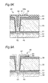
- FIG. 8K is a cross-sectional view at a time point when a protection layer is formed according to the semiconductor device manufacturing method of Conventional Example 1;
- FIG. 9A is a cross-sectional view of one example of the structure of the semiconductor device according to Conventional Example 1 before a protection film is formed;
- FIG. 9B is a view of two through-hole electrodes and a wiring between the through-hole electrodes in one example in the structure of the semiconductor device according to Conventional Example 1 as seen from above;
- FIG. 10 is a flowchart of a semiconductor device manufacturing method according to Conventional Example 2.
- FIG. 11A is a cross-sectional view at a time point when a support member is formed by bonding to the semiconductor substrate according to the semiconductor device manufacturing method of Conventional Example 2;
- FIG. 11B is a cross-sectional view at a time point when a resist for a through via hole is formed according to the semiconductor device manufacturing method of Conventional Example 2;
- FIG. 11C is a cross-sectional view at a time point when a through via hole is formed according to the semiconductor device manufacturing method of Conventional Example 2;
- FIG. 11D is a cross-sectional view at a time point when an insulating film layer is formed according to the semiconductor device manufacturing method of Conventional Example 2;
- FIG. 11E is a cross-sectional view at a time point when the insulating film is removed by etch back according to the semiconductor device manufacturing method of Conventional Example 2;
- FIG. 11F is a cross-sectional view at a time point when a barrier metal layer and a seed metal layer are formed according to the semiconductor device manufacturing method of Conventional Example 2;
- FIG. 11G is a cross-sectional view at a time point when a resist for a wiring is formed according to the semiconductor device manufacturing method of Conventional Example 2;
- FIG. 11H is a cross-sectional view at a time point when the wiring layer is formed in the semiconductor device manufacturing method of Conventional Example 2;
- FIG. 11I is a cross-sectional view at a time point when the resist is removed according to the semiconductor device manufacturing method of Conventional Example 2;
- FIG. 11J is a cross-sectional view at a time point when the seed metal layer and the barrier metal layer are removed in accordance with the semiconductor device manufacturing method of Conventional Example 2;
- FIG. 11K is a cross-sectional view at a time point when a protection layer is formed according to the semiconductor device manufacturing method of Conventional Example 2;
- FIG. 12A is a cross-sectional view of one example of the structure of the semiconductor device according to Conventional Example 2 before a protection film is formed;
- FIG. 12B is a view of two through-hole electrodes and a wiring between the through-hole electrodes in one example in the structure of the semiconductor device according to Conventional Example 2 as seen from above.
- FIG. 1 is the flowchart of the semiconductor device manufacturing method according to the first embodiment
- FIGS. 2A to 2N are cross-sectional views at respective stages (steps).
- a description will be given of the semiconductor device prepared in accordance with the manufacturing method with reference to FIGS. 3A , 3 B, and 3 C.
- a support member 4 is bonded on the front surfaces (the bottom surface in FIG. 2A ) of an electronic device 2 and a semiconductor substrate 5 , having a first insulating film 1 and a resin layer possessing an adhesion function (not shown) interposed therebetween (step S 101 ).
- the electronic device 2 is a light receiving element such as a CCD, an infrared sensor or the like, or a light emitting element, or the like, for example.
- a pad electrode 3 being an external connection-purpose electrode connected to the electronic device 2 is formed.
- the semiconductor substrate 5 is structured with a silicon substrate, for example.
- the resin layer possessing an adhesion function refers to an adhesion layer.
- the support member 4 should be bonded as necessary, and is not necessarily bonded.
- the insulating protection layer 3 A is a layer disposed to surround the pad electrode 3 .
- the hole electrode hole 7 a extending from the back surface of the semiconductor substrate 5 to reach the first insulating film 1 immediately above the pad electrode 3 is formed by dry etching (step S 103 ).
- the etching gas for example, a gas that contains SF 6 , O 2 , C 4 F 8 , or the like is used.
- the first insulating film 1 is exposed.
- the first insulating film 1 at the bottom portion of the via hole 7 a is removed by dry etching using the opening 6 a - 1 .
- the etching gas for example, a gas that contains CF 4 , O 2 , O 438 , or the like is used.
- the pad electrode 3 is partially exposed.
- the resist layer 6 a is removed from the back surface of the semiconductor substrate 5 .
- a frame-like dummy groove hole portion for forming insulating portion (one example of a groove for forming insulating portion) 7 b is formed.
- a resist pattern layer 6 b is formed (step S 201 ).
- the frame-like opening groove portion 6 b - 1 is formed.
- the resist pattern layer 6 b is formed to entirely bury the via hole 7 a.
- a second insulating film 8 is formed (step S 104 ).
- the thickness of the second insulating film 8 at the bottom portion of the via hole 7 a becomes thinner than the thickness of the second insulating film 8 formed on the back surface of the semiconductor substrate 5 , in accordance with the depth of the via hole 7 a .
- the thickness of the second insulating film 8 at the bottom portion of the dummy groove hole portion 7 b becomes thinner than the thickness of the second insulating film 8 formed on the back surface of the semiconductor substrate 5 , in accordance with the depth of the dummy groove hole portion 7 b.
- the second insulating film 8 is etched preferably by anisotropic dry etching (step S 105 ).
- anisotropic dry etching at the bottom portion of the via hole 7 a and the bottom portion of the dummy groove hole portion 7 b , the second insulating film 8 is removed to partially expose the pad electrode 3 .
- the second insulating film 8 remains at the back surface of the semiconductor substrate 5 , the side inner wall of the via hole 7 a , and the side inner wall of the dummy groove hole portion 7 b .
- a conductive barrier metal layer 9 is formed on the entire surface of the second, insulating film 8 including: the side inner wall of the via hole 7 a ; the side inner wall and the bottom surface of the dummy groove hole portion 7 b ; the back surface of the semiconductor substrate 5 ; and on the part of the pad electrode 3 exposed at the bottom portion of the via hole 7 a (step S 106 ).
- the barrier metal layer 9 is formed with a metal layer of, e.g., a titanium tungsten layer, a titanium nitride layer, a tantalum nitride layer, or the like.
- the barrier metal layer 9 is formed by a film growth method such as sputtering, CVD, or the like, for example.
- a conductive seed metal layer 10 is formed on the entire surface of the barrier metal layer 9 including: the side inner wall of the via hole 7 a ; the side inner wall and the bottom surface of the dummy groove hole portion 7 b ; the back surface of the semiconductor substrate 5 , and on the entire surface of the barrier metal layer 9 on the part of the pad electrode 3 exposed at the bottom portion of the via hole 7 a (step S 107 ).
- the seed metal layer 10 is a layer to be an electrode to form a wiring formation layer, whose description will be given later, by plating, and is structured with metal such as copper or the like.
- a second resist layer 12 is formed at a prescribed region on the seed metal layer 10 (step S 108 ).
- the prescribed region where the second resist layer 12 is to be formed is a region except for the formation region of the via hole 7 a .
- the prescribed region where the second resist layer 12 is to be formed is a region on the back surface of the semiconductor substrate 5 where a wiring layer 18 having a prescribed pattern, whose description will be given later, is not to be formed.
- the second resist layer 12 is formed to entirely bury the inside of the dummy groove hole portion 7 b.
- a wiring formation layer 11 is formed at the side inner wall and the bottom surface of the via hole 7 a , and a region on the back surface of the semiconductor substrate 5 where the wiring layer 18 is to be formed (step S 109 ).
- the wiring formation layer 11 is a metal layer structured with, e.g., copper, by the electrolytic plating process, for example.
- the second resist 12 is removed (step S 110 ).
- the asking process is used, for example.
- step S 203 the seed metal layer 10 and the barrier metal layer 9 at the bottom portion of the dummy groove hole portion 7 b b is removed.
- Patterning carried out by removal of the seed metal layer 10 and the barrier metal layer 9 is carried out by wet etching, for example.
- the thickness of the seed metal layer 10 not covered by the wiring formation layer 11 , the seed metal layer 10 at other portions such as at the back surface of the semiconductor substrate 5 and at the inner sidewall of the dummy groove hole portion 7 b , somewhat becomes thinner.
- the seed metal layer 10 and the barrier metal layer 9 removed by wet etching should be just those at the bottom portion of the dummy groove hole portion 7 b .
- the seed metal layer 10 and the barrier metal layer 9 on the back surface of the semiconductor substrate 5 may remain after patterning by wet etching is carried out.
- a protection layer 13 as one example of the insulating layer is formed on the entire back surface of the semiconductor substrate 5 including the inside of the via hole 7 a and the inside of the dummy groove hole portion 7 b , so as to cover them (step S 111 ).
- the entire back surface of the semiconductor substrate 5 refers to the top of the seed metal layer 10 and the wiring formation layer 11 and the like, i.e., the top of the through-hole electrode 19 (a conductor portion structured with a part of the wiring formation layer 11 , the seed metal layer 10 , and the barrier metal layer 9 ) and the wiring layer 18 .
- the protection layer 13 is structured with an insulating resist material or the like, for example.
- the protection layer 13 is provided with an opening 13 a at the position corresponding to the wiring layer 18 . Then, on the wiring layer 18 exposed at the opening 13 a , a ball-like conductive terminal 14 made of metal, e.g., solder or the like, is formed. It is to be noted that, at the bottom portion of the dummy groove hole portion 7 b , the insulating material of the protection layer 13 disposed in the dummy groove hole portion 7 b and the material structuring the semiconductor substrate are in direct contact with each other, so as to exhibit insulation. Hence, by the protection layer 13 being inserted into the dummy groove hole portion 7 b such that the dummy groove hole portion 7 b is filled therewith, a frame-like insulating portion 20 is formed.
- the semiconductor substrate 5 is subjected to dicing.
- a plurality of semiconductor devices each being a semiconductor chip having the through-hole electrode 19 is completed.
- FIGS. 3A and 3B each show one example of a part of the semiconductor device prepared in accordance with the manufacturing method described in the foregoing.
- FIGS. 3A and 3B show two through-hole electrodes 19 and the wiring layer 18 connecting between the through-hole electrodes 19 .
- FIGS. 3A and 33 each show a state before the protection film 13 is formed.
- FIG. 3A shows a cross-sectional structure of the through-hole electrode 19 .
- FIG. 35 schematically shows the structure of the two through-hole electrodes 19 and the wiring layer (rewiring layer) 18 connecting between the through-hole electrodes 19 as seen from above.
- the top portion of the semiconductor device is structured with the two through-hole electrodes 19 , a wiring portion 18 a connecting between the through-hole electrodes 19 , and a frame-like insulating portion 20 intended to insulate the two through-hole electrodes 19 and the wiring portion 18 a from the surrounding.
- the frame-like insulating portion 20 is disposed in a frame-like manner, so as to surround the two through-hole electrodes 19 and the wiring portion 18 a while being away from them by a prescribed interval.
- the disposition so as to surround the two through-hole electrodes 19 and the wiring portion 18 a while being away from them by a prescribed interval is, in other words, a disposition conforming to the outer shape of the two through-hole electrodes 19 and the wiring portion 18 a .
- a disposition conforming to the outer shape even in a case where each through-hole electrode 19 is arranged at a narrow pitch, a high-density wiring can be achieved.
- the frame-like insulating portion 20 is only required to surround the two through-hole electrodes 19 and the wiring portion 18 a , such that they are insulated from other through-hole electrode 19 or wiring portion 18 a .
- the insulating portion 20 is not limited to a frame-like shape conforming to the outer shape of the two through-hole electrodes 19 and the wiring portion 18 a , and it may be a simple quadrilateral shape, an oval shape or the like.
- the wiring layer 18 structures the wiring portion 18 a that functions as a rewiring layer electrically connecting a plurality of through-hole electrodes 19 to one another, for example. It is to be noted that, as shown in FIG. 3C , the wiring layer 18 may be structured to further include external terminals 18 b , second wiring portions 18 c connecting between the external terminals 18 b and the through-hole electrode 19 or the wiring portion 18 a . That is, FIG. 3C schematically shows the structure of the wiring layer 18 including the two through-hole electrodes 19 , the wiring portion 18 a connecting between the through-hole electrodes 19 , the external terminals 18 b , the second wiring portions 18 c connecting between the external terminals 18 b and the through-hole electrodes 19 as seen from above.
- the top portion of the semiconductor device is structured with the two through-hole electrodes 19 , two wiring layers 18 a and second wiring portions 18 c , the external terminals 18 b , and the frame-like insulating portion 20 intended to insulate them from the surrounding.
- the present embodiment is capable of drastically shortening the wet etching time to be as 1/10 to 1 ⁇ 5 (i.e., 2 to 6 minutes) as compared with the wet etching time (20 to 30 minutes) disclosed in Conventional Example 2. Accordingly, it becomes possible to provide a semiconductor device and a manufacturing method thereof that can drastically reduce the processing time and processing cost for the wet etching step of the wiring formation layer 11 , the seed metal layer 10 , and the barrier metal layer 9 . It is to be noted that, of Conventional Examples 1 and 2, Conventional Example 2 is a conventional example that is advantageous in terms of the processing time of the wet etching step of the wiring formation layer 11 , the seed metal layer 10 , and the barrier metal layer 9 .
- the semiconductor device of the present embodiment has the frame-like insulating portion 20 that surrounds the through-hole electrode 19 and the wiring layer 18 on the back surface of the semiconductor substrate 5 , the frame-like insulating portion 20 insulating from other through-hole electrode 19 and rewiring layer 18 . Therefore, structuring the insulating material of the frame-like insulating portion 20 , that is, the material of the protection layer 13 , with a resin material such as resist that is softer than the semiconductor substrate 5 , e.g., silicon of the silicon substrate, it becomes possible to provide the function of stress relaxation. In this case, the stress acting on the semiconductor device can be relieved by the insulating material inside the frame-like insulating portion 20 .
- FIG. 4 a flowchart is shown in FIG. 4 , and cross-sectional views at respective stages (steps) are shown in FIGS. 5A to 5L .
- FIGS. 5A to 5L cross-sectional views at respective stages (steps) are shown in FIGS. 5A to 5L .
- FIGS. 6A and 6B a description will be given with reference to FIGS. 6A and 6B .
- a support member 4 is bonded to the front surfaces (the bottom surface in FIG. 5A ) of an electronic device 2 and a semiconductor substrate 5 , having a first insulating film 1 and a resin layer possessing an adhesion function (not shown) interposed therebetween (step S 101 ).
- the electronic device 2 is a light receiving element, such as a CCD, an infrared sensor or the like, or a light emitting element, or the like, for example.
- a pad electrode 3 being an external connection-purpose electrode connected to the electronic device 2 is formed.
- the semiconductor substrate 5 is structured with a silicon substrate, for example.
- the resin layer possessing an adhesion function refers to an adhesion layer.
- the support member 4 may be bonded as necessary, and is not necessarily bonded.
- the insulating protection layer 3 A is a layer disposed to surround the pad electrode 3 .
- a through-hole electrode forming-purpose via hole 7 a that penetrates through the semiconductor substrate 5 to reach the first insulating film 1 immediately above the pad electrode 3 and a frame-like insulating portion forming-purpose dummy groove hole portion (one example of the groove for forming insulating portion) 7 b are formed.
- a resist layer (a resist via pattern layer) 6 is formed (step S 204 ).
- the resist layer 6 is provided with an opening 6 - 1 at a portion where the via hole 7 a is to be formed.
- the resist layer 6 is provided with a frame-like opening groove portion 6 - 2 at a portion where the dummy groove hole portion 7 b is to be formed.
- the frame-like opening groove portion 6 - 2 for the dummy groove hole portion 7 b is set to be smaller than the resist opening 6 - 1 for the via hole 7 a.
- the hole electrode hole 7 a extending from the back surface of the semiconductor substrate 5 to reach the first insulating film 1 immediately above the pad electrode 3 , and the dummy groove hole portion 7 b are formed simultaneously by dry etching (step S 205 ).
- the etching gas for example, a gas that contains SF 5 , O 2 , C 4 F 8 , or the like is used. At the bottom portion of the via hole 7 a , the first insulating film 1 is exposed.
- the frame-like opening groove portion 6 - 2 of the dummy groove hole portion 7 b is set to be smaller than the opening 6 - 1 for the via hole 7 a , the dummy groove hole portion 7 b will not penetrate through the semiconductor substrate 5 .
- the first insulating film 1 at the bottom portion of the via hole 7 a is removed by dry etching.
- the etching gas for example, a gas that contains CF 4 , O 2 , C 4 F 8 , or the like is used.
- the resist layer 6 is removed from the back surface of the semiconductor substrate 5 .
- a second insulating film 8 is formed (step S 104 ).
- the thickness of the second insulating film 8 at the bottom portion of the via hole 7 a becomes thinner than the thickness of the second insulating film 8 formed at the back surface of the semiconductor substrate 5 in accordance with the depth of the via hole 7 a .
- the thickness of the second insulating film 8 at the bottom portion of the dummy groove hole portion 7 b also becomes thinner than the thickness of the second insulating film 8 formed on the back surface of the semiconductor substrate 5 in accordance with the depth of the dummy groove hole portion 7 b.
- the second insulating film 8 is etched preferably by anisotropic dry etching (step S 105 ).
- anisotropic dry etching at the bottom portion of the via hole 7 a and at the bottom portion of the dummy groove hole portion 7 b , the second insulating film 8 is removed to partially expose the pad electrode 3 .
- the second insulating film 8 remains at the back surface of the semiconductor substrate 5 , the side inner wall of the via hole 7 a , and the side inner wall of the dummy groove hole portion 7 b .
- a conductive barrier metal layer 9 is formed on the entire surface of the second insulating film 8 including: the side inner wall of the via hole 7 a ; the side inner wall and the bottom surface of the dummy groove hole portion 7 b ; and the back surface of the semiconductor substrate 5 , and the part of the pad electrode 3 exposed at the bottom portion of the via hole 7 a (step S 106 ).
- the barrier metal layer 9 is formed with a metal layer of, e.g., a titanium tungsten layer, a titanium nitride layer, a tantalum nitride layer, or the like.
- the barrier metal layer 9 is formed by a film growth method such as sputtering, CVD, or the like.
- a conductive seed metal layer 10 is formed on the entire surface of the barrier metal layer 9 including: the side inner wall of the via hole 7 a ; the side inner wall and the bottom surface of the dummy groove hole portion 7 b ; the back surface of the semiconductor substrate 5 , and on the entire surface of the barrier metal layer 9 on the part of the pad electrode 3 exposed at the bottom portion of the via hole 7 a (step S 107 ).
- the seed metal layer 10 is to be an electrode to form a wiring formation layer, whose description will be given later, by plating, and is structured with metal such as copper or the like, for example.
- a second resist layer 12 is formed at a prescribed region on the seed metal layer 10 (step S 108 ).
- the prescribed region where the second resist layer 12 is formed is a region except for a formation region of the via hole 7 a .
- the prescribed region where the second resist layer 12 is formed is a region on the back surface of the semiconductor substrate 5 where a wiring layer 18 having a prescribed pattern, whose description will be given later, is not formed.
- the second resist layer 12 is formed to entirely bury the inside of the dummy groove hole portion 7 b.
- a wiring formation layer 11 is formed at the side inner wall and the bottom surface of the via hole 7 a , and a region on the back surface of the semiconductor substrate 5 where the wiring layer 18 is to be formed (step S 109 ).
- the wiring formation layer 11 is a metal layer structured with, e.g., copper, by the electrolytic plating process, for example.
- the second resist layer 12 is removed (step S 110 ).
- the ashing process is used, for example.
- the seed metal layer 10 and the barrier metal layer 9 at the bottom portion of the dummy groove hole portion 7 b are removed (step S 203 ).
- Patterning carried out by the removal of the seed metal layer 10 and the barrier metal layer 9 is carried out by wet etching, for example.
- the thickness of the seed metal layer 10 not covered by the wiring formation layer 11 , the seed metal layer 10 at other portions such as at the back surface of the semiconductor substrate 5 and at the inner sidewall of the dummy groove hole portion 7 b somewhat becomes thinner.
- the seed metal layer 10 and the barrier metal layer 9 removed by wet etching may be just those at the bottom portion of the dummy groove hole portion 7 b . That is, the seed metal layer 10 and the barrier metal layer 9 on the back surface of the semiconductor substrate 5 may remain.
- a protection layer 13 is formed on the entire back surface of the semiconductor substrate 5 including the inside of the via hole 7 a and the inside of the dummy groove hole portion 7 b , so as to cover them (step S 111 ).
- the entire back surface of the semiconductor substrate 5 refers to the top of the seed metal layer 10 and the wiring formation layer 11 and the like, i.e., the top of the through-hole electrode 19 (a conductor portion structured with a part of the wiring formation layer 11 , the seed metal layer 10 , and the barrier metal layer 9 ) and the wiring layer 18 .
- the protection layer 13 is structured with an insulating resist material or the like, for example.
- the protection layer 13 is provided with an opening 13 a at the position corresponding to the wiring layer 18 . Then, on the wiring layer 18 exposed at the opening 13 a , a ball-like conductive terminal 14 made of metal, e.g., solder or the like, is formed. It is to be noted that, at the bottom portion of the dummy groove hole portion 7 b , the insulating material of the protection layer 13 disposed in the dummy groove hole portion 7 b and the material structuring the semiconductor substrate 5 are in direct contact with each other, so as to exhibit insulation. Hence, by the protection layer 13 being inserted into the dummy groove hole portion 7 b such that the dummy groove hole portion 7 b is filled therewith, a frame-like insulating portion 20 can be formed.
- the semiconductor substrate 5 is subjected to dicing.
- a plurality of semiconductor devices each being a semiconductor chip having the through-hole electrode 19 is completed.
- FIGS. 6A and 6B each show one example of a part of the semiconductor device prepared in accordance with the manufacturing method described in the foregoing.
- FIGS. 6A and 6B show two through-hole electrodes 19 and the wiring layer 18 connecting between the through-hole electrodes 19 , in a state before the protection film 13 is formed.
- FIG. 6A shows a cross-sectional structure of the through-hole electrode 19
- FIG. 6B schematically shows the structure of the two through-hole electrodes 19 and the wiring layer 18 connecting between the through-hole electrodes 19 as seen from above.
- the top portion of the semiconductor device is structured with the two through-hole electrodes 19 , a wiring layer 18 connecting between the through-hole electrodes 19 , and a frame-like insulating portion 20 intended to insulate the two through-hole electrodes 19 and the wiring portion 18 a from the surrounding.
- the frame-like insulating portion 20 is disposed in a frame-like manner, so as to surround the two through-hole electrodes 19 and the wiring portion 18 a from the surrounding while being away from them by a prescribed interval.
- the disposition so as to surround the two through-hole electrodes 19 and the wiring portion 18 a while being away from them by a prescribed interval is, in other words, a disposition conforming to the outer shape of the two through-hole electrodes 19 and the wiring portion 18 a .
- a disposition conforming to the outer shape even in a case where each through-hole electrode 19 is arranged at a narrow pitch, a high-density wiring can be achieved.
- the frame-like insulating portion 20 is only required to surround the two through-hole electrodes 19 and the wiring portion 18 a , such that they are insulated from other through-hole electrode 19 or wiring portion 18 a .
- the frame-like insulating portion 20 is not limited to a frame-like shape conforming to the outer shape of the two through-hole electrodes 19 and the wiring portion 18 a , and it may be a simple quadrilateral shape, an oval shape or the like.
- the wiring layer 18 is formed to structure the wiring portion 18 a that functions as a rewiring layer electrically connecting a plurality of through-hole electrodes 19 to one another, for example. It is to be noted that, as it is for FIG. 3C , the wiring layer 18 may be structured to further include external terminals 18 b , and second wiring portions 18 c connecting between the external terminals 18 b and the through-hole electrode 19 or the wiring portion 11 a.
- the present invention requires drastically shortened wet etching time which is 1/10 to 1 ⁇ 5 (i.e., 2 to 6 minutes) as compared with that (20 to 30 minutes) disclosed in Conventional Example 2.
- Conventional Example 2 is an example that is advantageous in terms of the processing time of the wet etching step of the wiring formation layer 11 , the seed metal layer 10 , and the barrier metal layer 9 . Accordingly, it becomes possible to provide a semiconductor device and a manufacturing method thereof that can drastically reduce the processing time and processing cost for the wet etching step of the wiring formation layer 11 , the seed metal layer 10 , and the barrier metal layer 9 .
- the wet etching time is shortened, a great reduction in the thinning of the wiring formation layer 11 when the seed metal layer 10 and the barrier metal layer 9 are subjected to wet etching can be achieved, and a drastic reduction in the variation of the electric characteristic can be achieved. Accordingly, a semiconductor device and a manufacturing method thereof being high in the reliability of the electric characteristic can be provided.
- the dummy groove hole portion 7 b can be formed simultaneously with the formation step of the through-hole electrode-purpose via hole 7 a , an increase in the processing time and processing cost due to an increase in the number of steps will not occur in the dummy groove hole portion 7 b.
- the through hole diameter of the opening (the opening on the back surface of the semiconductor substrate 5 ) of the via hole 7 a forming the through-hole electrode 19 is ⁇ 1 ; and the groove width of the opening (the opening on the back surface of the semiconductor substrate 5 ) of the dummy groove hole portion 7 b insulating between the wirings is L 2 , it is desirable that the dummy groove hole portion 7 b is formed such that the through hole diameter ⁇ 1 and the groove width L 2 satisfy the following relational expression:
- the width L 2 of the dummy groove hole portion 7 b exceeds ⁇ 1 /2, the dummy groove hole portion 7 b may penetrate through the semiconductor substrate 5 .
- Another reason for that is to set the width L 2 of the dummy groove hole portion 7 b to assume a value greater than 0, because it is essential to form the dummy groove hole portion 7 b.
- the semiconductor device and the manufacturing method thereof of the present invention can reduce the processing time. Therefore, in particular, it is useful as a semiconductor device having a through-hole electrode and a manufacturing method thereof, e.g., a BGA-type semiconductor device having a through-hole electrode being one type of CSP, and a manufacturing method thereof.
Landscapes
- Engineering & Computer Science (AREA)
- Computer Hardware Design (AREA)
- Microelectronics & Electronic Packaging (AREA)
- Power Engineering (AREA)
- Physics & Mathematics (AREA)
- Condensed Matter Physics & Semiconductors (AREA)
- General Physics & Mathematics (AREA)
- Manufacturing & Machinery (AREA)
- Internal Circuitry In Semiconductor Integrated Circuit Devices (AREA)
Applications Claiming Priority (3)
| Application Number | Priority Date | Filing Date | Title |
|---|---|---|---|
| JP2010124013A JP5352534B2 (ja) | 2010-05-31 | 2010-05-31 | 半導体装置及びその製造方法 |
| JP2010-124013 | 2010-05-31 | ||
| PCT/JP2011/001825 WO2011151961A1 (ja) | 2010-05-31 | 2011-03-28 | 半導体装置及びその製造方法 |
Publications (1)
| Publication Number | Publication Date |
|---|---|
| US20120119384A1 true US20120119384A1 (en) | 2012-05-17 |
Family
ID=45066355
Family Applications (1)
| Application Number | Title | Priority Date | Filing Date |
|---|---|---|---|
| US13/387,204 Abandoned US20120119384A1 (en) | 2010-05-31 | 2011-03-28 | Semiconductor device and manufacturing method thereof |
Country Status (4)
| Country | Link |
|---|---|
| US (1) | US20120119384A1 (enExample) |
| JP (1) | JP5352534B2 (enExample) |
| CN (1) | CN102473640A (enExample) |
| WO (1) | WO2011151961A1 (enExample) |
Cited By (5)
| Publication number | Priority date | Publication date | Assignee | Title |
|---|---|---|---|---|
| US20110193241A1 (en) * | 2010-02-09 | 2011-08-11 | Yu-Lin Yen | Chip package and method for forming the same |
| WO2015147620A1 (fr) * | 2013-10-14 | 2015-10-01 | Nemotek Technologies S.A | Procédé de métallisation en cuivre destiné à la fabrication d'un circuit intégré en utilisant la technologie wafer level packaging 3d |
| US20180122749A1 (en) * | 2016-11-01 | 2018-05-03 | Advanced Semiconductor Engineering, Inc. | Semiconductor wafer, semiconductor package and method for manufacturing the same |
| US10026715B2 (en) | 2015-03-17 | 2018-07-17 | Toshiba Memory Corporation | Semiconductor device and manufacturing method thereof |
| US10763163B2 (en) | 2018-07-19 | 2020-09-01 | Samsung Electronics Co., Ltd. | Integrated circuit device and method of manufacturing the same |
Families Citing this family (5)
| Publication number | Priority date | Publication date | Assignee | Title |
|---|---|---|---|---|
| US9437783B2 (en) * | 2012-05-08 | 2016-09-06 | Cree, Inc. | Light emitting diode (LED) contact structures and process for fabricating the same |
| CN103367139B (zh) * | 2013-07-11 | 2016-08-24 | 华进半导体封装先导技术研发中心有限公司 | 一种tsv孔底部介质层刻蚀方法 |
| JP7067448B2 (ja) * | 2018-12-10 | 2022-05-16 | 三菱電機株式会社 | 半導体装置の製造方法、半導体装置 |
| JP2020098849A (ja) | 2018-12-18 | 2020-06-25 | ソニーセミコンダクタソリューションズ株式会社 | 半導体装置 |
| CN112185984B (zh) * | 2020-09-17 | 2022-07-12 | 武汉华星光电半导体显示技术有限公司 | 一种阵列基板及显示面板 |
Citations (5)
| Publication number | Priority date | Publication date | Assignee | Title |
|---|---|---|---|---|
| US20090284631A1 (en) * | 2007-12-27 | 2009-11-19 | Mie Matsuo | Semiconductor package and camera module |
| US20100127403A1 (en) * | 2008-11-26 | 2010-05-27 | Canon Kabushiki Kaisha | Semiconductor apparatus manufacturing method and semiconductor apparatus |
| US7906430B2 (en) * | 2004-09-29 | 2011-03-15 | Sanyo Electric Co., Ltd. | Method of manufacturing a semiconductor device with a peeling prevention layer |
| US20110092065A1 (en) * | 2003-01-15 | 2011-04-21 | Fujitsu Semiconductor Limited | Semiconductor device suitable for a stacked structure |
| US7968429B2 (en) * | 2004-03-29 | 2011-06-28 | Hamamatsu Photonics K.K. | Method of manufacturing a semiconductor photodetector device by removing the semiconductor substrate on one surface after forming the light-transmitting layer on the opposing surface |
Family Cites Families (6)
| Publication number | Priority date | Publication date | Assignee | Title |
|---|---|---|---|---|
| JPS5829624B2 (ja) * | 1978-09-11 | 1983-06-23 | 富士通株式会社 | 架橋配線方法 |
| JP2003198122A (ja) * | 2001-12-28 | 2003-07-11 | Kanegafuchi Chem Ind Co Ltd | 配線板の製造方法 |
| TWI303864B (en) * | 2004-10-26 | 2008-12-01 | Sanyo Electric Co | Semiconductor device and method for making the same |
| JP5036127B2 (ja) * | 2004-10-26 | 2012-09-26 | オンセミコンダクター・トレーディング・リミテッド | 半導体装置の製造方法 |
| US7633167B2 (en) * | 2005-09-29 | 2009-12-15 | Nec Electronics Corporation | Semiconductor device and method for manufacturing same |
| JP5021992B2 (ja) * | 2005-09-29 | 2012-09-12 | ルネサスエレクトロニクス株式会社 | 半導体装置およびその製造方法 |
-
2010
- 2010-05-31 JP JP2010124013A patent/JP5352534B2/ja not_active Expired - Fee Related
-
2011
- 2011-03-28 US US13/387,204 patent/US20120119384A1/en not_active Abandoned
- 2011-03-28 CN CN2011800030798A patent/CN102473640A/zh active Pending
- 2011-03-28 WO PCT/JP2011/001825 patent/WO2011151961A1/ja not_active Ceased
Patent Citations (5)
| Publication number | Priority date | Publication date | Assignee | Title |
|---|---|---|---|---|
| US20110092065A1 (en) * | 2003-01-15 | 2011-04-21 | Fujitsu Semiconductor Limited | Semiconductor device suitable for a stacked structure |
| US7968429B2 (en) * | 2004-03-29 | 2011-06-28 | Hamamatsu Photonics K.K. | Method of manufacturing a semiconductor photodetector device by removing the semiconductor substrate on one surface after forming the light-transmitting layer on the opposing surface |
| US7906430B2 (en) * | 2004-09-29 | 2011-03-15 | Sanyo Electric Co., Ltd. | Method of manufacturing a semiconductor device with a peeling prevention layer |
| US20090284631A1 (en) * | 2007-12-27 | 2009-11-19 | Mie Matsuo | Semiconductor package and camera module |
| US20100127403A1 (en) * | 2008-11-26 | 2010-05-27 | Canon Kabushiki Kaisha | Semiconductor apparatus manufacturing method and semiconductor apparatus |
Cited By (7)
| Publication number | Priority date | Publication date | Assignee | Title |
|---|---|---|---|---|
| US20110193241A1 (en) * | 2010-02-09 | 2011-08-11 | Yu-Lin Yen | Chip package and method for forming the same |
| US9559001B2 (en) * | 2010-02-09 | 2017-01-31 | Xintec Inc. | Chip package and method for forming the same |
| WO2015147620A1 (fr) * | 2013-10-14 | 2015-10-01 | Nemotek Technologies S.A | Procédé de métallisation en cuivre destiné à la fabrication d'un circuit intégré en utilisant la technologie wafer level packaging 3d |
| US10026715B2 (en) | 2015-03-17 | 2018-07-17 | Toshiba Memory Corporation | Semiconductor device and manufacturing method thereof |
| US20180122749A1 (en) * | 2016-11-01 | 2018-05-03 | Advanced Semiconductor Engineering, Inc. | Semiconductor wafer, semiconductor package and method for manufacturing the same |
| US10763163B2 (en) | 2018-07-19 | 2020-09-01 | Samsung Electronics Co., Ltd. | Integrated circuit device and method of manufacturing the same |
| US11488860B2 (en) | 2018-07-19 | 2022-11-01 | Samsung Electronics Co., Ltd. | Integrated circuit device and method of manufacturing the same |
Also Published As
| Publication number | Publication date |
|---|---|
| CN102473640A (zh) | 2012-05-23 |
| JP2011249718A (ja) | 2011-12-08 |
| WO2011151961A1 (ja) | 2011-12-08 |
| JP5352534B2 (ja) | 2013-11-27 |
Similar Documents
| Publication | Publication Date | Title |
|---|---|---|
| US20120119384A1 (en) | Semiconductor device and manufacturing method thereof | |
| US7732925B2 (en) | Semiconductor device and manufacturing method thereof | |
| JP4873517B2 (ja) | 半導体装置及びその製造方法 | |
| US8841751B2 (en) | Through silicon vias for semiconductor devices and manufacturing method thereof | |
| US9165898B2 (en) | Method of manufacturing semiconductor device with through hole | |
| KR100679572B1 (ko) | 반도체 장치의 제조 방법 | |
| US8159071B2 (en) | Semiconductor package with a metal post | |
| US20100032830A1 (en) | Three-dimensional conducting structure and method of fabricating the same | |
| US8018032B2 (en) | Silicon substrate and chip package structure with silicon base having stepped recess for accommodating chip | |
| JP4775007B2 (ja) | 半導体装置及びその製造方法 | |
| US8450844B2 (en) | Semiconductor package and method of manufacturing the same | |
| US7557017B2 (en) | Method of manufacturing semiconductor device with two-step etching of layer | |
| US20160020191A1 (en) | Functional Spacer for SIP and Methods for Forming the Same | |
| US20180122721A1 (en) | Plug structure of a semiconductor chip and method of manufacturing the same | |
| US9437457B2 (en) | Chip package having a patterned conducting plate and method for forming the same | |
| JP4845986B2 (ja) | 半導体装置 | |
| US20110108993A1 (en) | Semiconductor package and manufacturing method thereof | |
| US8716843B2 (en) | Microelectronic chip, component containing such a chip and manufacturing method | |
| JP2010165921A (ja) | 半導体プロセス、ならびにそれを適用したシリコン基材およびチップパッケージ構造 |
Legal Events
| Date | Code | Title | Description |
|---|---|---|---|
| AS | Assignment |
Owner name: PANASONIC CORPORATION, JAPAN Free format text: ASSIGNMENT OF ASSIGNORS INTEREST;ASSIGNORS:TAKII, YOSHIMASA;KAI, TAKAYUKI;SAITO, DAISHIRO;AND OTHERS;SIGNING DATES FROM 20111206 TO 20111213;REEL/FRAME:027975/0769 |
|
| STCB | Information on status: application discontinuation |
Free format text: ABANDONED -- FAILURE TO RESPOND TO AN OFFICE ACTION |