US20090146292A1 - Semiconductor device thermal connection - Google Patents
Semiconductor device thermal connection Download PDFInfo
- Publication number
- US20090146292A1 US20090146292A1 US11/950,819 US95081907A US2009146292A1 US 20090146292 A1 US20090146292 A1 US 20090146292A1 US 95081907 A US95081907 A US 95081907A US 2009146292 A1 US2009146292 A1 US 2009146292A1
- Authority
- US
- United States
- Prior art keywords
- semiconductor device
- thermal connection
- thermal
- thermal conductivity
- carbon fiber
- Prior art date
- Legal status (The legal status is an assumption and is not a legal conclusion. Google has not performed a legal analysis and makes no representation as to the accuracy of the status listed.)
- Granted
Links
Images


Classifications
-
- H—ELECTRICITY
- H10—SEMICONDUCTOR DEVICES; ELECTRIC SOLID-STATE DEVICES NOT OTHERWISE PROVIDED FOR
- H10W—GENERIC PACKAGES, INTERCONNECTIONS, CONNECTORS OR OTHER CONSTRUCTIONAL DETAILS OF DEVICES COVERED BY CLASS H10
- H10W40/00—Arrangements for thermal protection or thermal control
- H10W40/20—Arrangements for cooling
- H10W40/25—Arrangements for cooling characterised by their materials
- H10W40/255—Arrangements for cooling characterised by their materials having a laminate or multilayered structure, e.g. direct bond copper [DBC] ceramic substrates
-
- H—ELECTRICITY
- H10—SEMICONDUCTOR DEVICES; ELECTRIC SOLID-STATE DEVICES NOT OTHERWISE PROVIDED FOR
- H10W—GENERIC PACKAGES, INTERCONNECTIONS, CONNECTORS OR OTHER CONSTRUCTIONAL DETAILS OF DEVICES COVERED BY CLASS H10
- H10W40/00—Arrangements for thermal protection or thermal control
- H10W40/20—Arrangements for cooling
- H10W40/25—Arrangements for cooling characterised by their materials
- H10W40/257—Arrangements for cooling characterised by their materials having a heterogeneous or anisotropic structure, e.g. powder or fibres in a matrix, wire mesh or porous structures
-
- H—ELECTRICITY
- H10—SEMICONDUCTOR DEVICES; ELECTRIC SOLID-STATE DEVICES NOT OTHERWISE PROVIDED FOR
- H10W—GENERIC PACKAGES, INTERCONNECTIONS, CONNECTORS OR OTHER CONSTRUCTIONAL DETAILS OF DEVICES COVERED BY CLASS H10
- H10W72/00—Interconnections or connectors in packages
- H10W72/30—Die-attach connectors
-
- H—ELECTRICITY
- H10—SEMICONDUCTOR DEVICES; ELECTRIC SOLID-STATE DEVICES NOT OTHERWISE PROVIDED FOR
- H10W—GENERIC PACKAGES, INTERCONNECTIONS, CONNECTORS OR OTHER CONSTRUCTIONAL DETAILS OF DEVICES COVERED BY CLASS H10
- H10W72/00—Interconnections or connectors in packages
- H10W72/071—Connecting or disconnecting
- H10W72/073—Connecting or disconnecting of die-attach connectors
- H10W72/07351—Connecting or disconnecting of die-attach connectors characterised by changes in properties of the die-attach connectors during connecting
- H10W72/07355—Connecting or disconnecting of die-attach connectors characterised by changes in properties of the die-attach connectors during connecting changes in materials
-
- H—ELECTRICITY
- H10—SEMICONDUCTOR DEVICES; ELECTRIC SOLID-STATE DEVICES NOT OTHERWISE PROVIDED FOR
- H10W—GENERIC PACKAGES, INTERCONNECTIONS, CONNECTORS OR OTHER CONSTRUCTIONAL DETAILS OF DEVICES COVERED BY CLASS H10
- H10W72/00—Interconnections or connectors in packages
- H10W72/30—Die-attach connectors
- H10W72/351—Materials of die-attach connectors
- H10W72/352—Materials of die-attach connectors comprising metals or metalloids, e.g. solders
- H10W72/3528—Intermetallic compounds
-
- H—ELECTRICITY
- H10—SEMICONDUCTOR DEVICES; ELECTRIC SOLID-STATE DEVICES NOT OTHERWISE PROVIDED FOR
- H10W—GENERIC PACKAGES, INTERCONNECTIONS, CONNECTORS OR OTHER CONSTRUCTIONAL DETAILS OF DEVICES COVERED BY CLASS H10
- H10W72/00—Interconnections or connectors in packages
- H10W72/90—Bond pads, in general
- H10W72/931—Shapes of bond pads
-
- H—ELECTRICITY
- H10—SEMICONDUCTOR DEVICES; ELECTRIC SOLID-STATE DEVICES NOT OTHERWISE PROVIDED FOR
- H10W—GENERIC PACKAGES, INTERCONNECTIONS, CONNECTORS OR OTHER CONSTRUCTIONAL DETAILS OF DEVICES COVERED BY CLASS H10
- H10W90/00—Package configurations
- H10W90/701—Package configurations characterised by the relative positions of pads or connectors relative to package parts
- H10W90/731—Package configurations characterised by the relative positions of pads or connectors relative to package parts of die-attach connectors
- H10W90/734—Package configurations characterised by the relative positions of pads or connectors relative to package parts of die-attach connectors between a chip and a stacked insulating package substrate, interposer or RDL
-
- H—ELECTRICITY
- H10—SEMICONDUCTOR DEVICES; ELECTRIC SOLID-STATE DEVICES NOT OTHERWISE PROVIDED FOR
- H10W—GENERIC PACKAGES, INTERCONNECTIONS, CONNECTORS OR OTHER CONSTRUCTIONAL DETAILS OF DEVICES COVERED BY CLASS H10
- H10W90/00—Package configurations
- H10W90/701—Package configurations characterised by the relative positions of pads or connectors relative to package parts
- H10W90/731—Package configurations characterised by the relative positions of pads or connectors relative to package parts of die-attach connectors
- H10W90/736—Package configurations characterised by the relative positions of pads or connectors relative to package parts of die-attach connectors between a chip and a stacked lead frame, conducting package substrate or heat sink
Definitions
- the invention relates to the field of thermal control for semiconductor devices.
- a semiconductor device thermal connection includes: a metallic barrier layer on semiconductor material of a semiconductor device; and a high thermal conductivity material on the metallic barrier layer that joins the semiconductor to a high conductivity thermal heat spreader lid attached to the semiconductor device.
- a semiconductor device thermal connection includes: a compressible carbon fiber solid carbon velvet material between a high thermal conductivity heat spreader lid and a heat sink; and a diaphragm enclosing the compressible carbon fiber solid material.
- a method of making a thermal connection to a semiconductor material includes the steps of: sputtering a metallic barrier material on a surface of the semiconductor material; and melting and re-solidifying a metallic high thermal conductivity material on the metallic barrier material.
- the metallic barrier material prevents migration of the metallic high thermal conductivity material into the semiconductor material and promotes adhesion of the high thermal conductivity material to the semiconductor material.
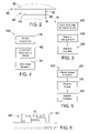
- FIG. 1 is a cross section view of a semiconductor device installation in accordance with an embodiment of the invention
- FIG. 2 is a cross section view of a portion of the installation of FIG. 1 ;
- FIG. 3 is a high-level flow chart of steps in the formation of the semiconductor device installation of FIG. 1 ;
- FIG. 4 is a flow chart showing further details of one of the steps of the method of FIG. 3 , forming a thermally-enhanced integrated circuit;
- FIG. 5 is a flow chart showing further details of another of the steps of the method of FIG. 3 , joining the integrated circuit and a wiring board with a heat sink;
- FIG. 6 is a cross section view of an alternate embodiment in accordance with the present invention, using a heat spreader with channels to allow flow of a cooling fluid;
- FIG. 7 is an oblique view showing configuration of multiple semiconductor device installations of FIG. 1 in a missile
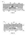
- FIG. 8 is a cross section view of another alternate embodiment semiconductor device installation in accordance with the present invention.
- FIG. 9 is a cross section view of another alternate embodiment semiconductor device installation in accordance with the present invention.
- a semiconductor device thermal connection used to remove heat from a semiconductor device includes a metallic barrier layer on the semiconductor device, and a high thermal conductivity material on the metallic barrier layer that joins the semiconductor to a high conductivity thermal heat spreader lid attached to the semiconductor device.
- the metallic barrier layer may be a sputtered layer
- the high thermal conductivity material may be a metallic material, for instance including indium, that is soldered onto the sputtered material.
- the soldered high thermal conductivity material may form an intermetallic with the material of the sputtered layer.
- the high thermal conductivity material may form a primary thermal connection in conducting heat away from the semiconductor device. The heat may be conducted into a high thermal conductivity heat spreader, such as a plate made of copper.
- the barrier layer prevents migration of the high thermal conductivity material into the semiconductor device. This allows the high thermal conductivity material to include metals that would possibly interfere with proper performance of the semiconductor device, if these materials were to migrate into the semiconductor device.
- the high thermal conductivity material may be a material with a relatively low melting temperature, for instance a solder including indium. Use of a low melting temperature material reduces stresses on the semiconductor device, relative to materials with higher melting points.
- a secondary thermal connection may be made between the heat spreader and a heat sink.
- the secondary thermal connection may include a solid (carbon velvet) carbon fiber material that is coupled to both of the heat spreader and a heat sink.
- a suitable adhesive such as a phase change adhesive, may be used to mechanically couple the carbon fiber material to the heat spreader.
- a diaphragm or membrane may be used to contain the carbon fiber material, to prevent electrically-conductive carbon fibers from coming into contact with the semiconductor device.
- the carbon fiber thermal connection advantageously is compressible, allowing for the secondary thermal connection to vary to some degree in thickness. This aids in compensating for variations in thickness of the semiconductor device package.
- FIG. 1 shows a semiconductor device installation 10 , coupling a semiconductor device 12 such as an integrated circuit, microprocessor die, and/or other electronic components, to a structure 14 .
- the structure 14 is a missile skin, although it will be appreciated that any of a wide variety of structures are encompassed by the structure 14 .
- the semiconductor device 12 is attached to a ceramic substrate 18 , which in turn is electrically coupled to a printed wiring board 20 through a ball grid array 22 .
- Epoxy corner parts 24 attach to both the semiconductor device 12 and the ceramic substrate 18 .
- the corner parts 24 aid in mechanically coupling the semiconductor device or integrated circuit 12 to the ceramic substrate 14 .
- a primary thermal interface 26 is attached to a top surface 28 of the semiconductor device 12 .
- the primary thermal interface 26 provides a path for conducting heat created by the semiconductor device 12 , from the device 12 to a heat spreader 30 .
- the heat spreader 30 and the semiconductor device 12 are attached to opposite major surfaces of the primary thermal interface 26 .
- the heat spreader 30 may be a copper structure that includes a planar member having a larger surface area than both the primary thermal interface 26 and the top surface 28 of the semiconductor device 12 .
- the heat spreader may be made of copper alloys, metal matrix composites, or other suitable high thermal conductivity material.
- the heat spreader 30 provides a high conductivity large surface area interface for conducting heat away from a semiconductor device 12 .
- the heat spreader 30 may have 12 times the area of the semiconductor device or integrated circuit 12 , although it will be appreciated that there are a large variety of possible areas for the heat spreader 30 .
- the heat spreader 30 includes a planar member 32 and a series of pillars 34 .
- the pillars 34 allow attachment of the heat spreader 30 to the ceramic substrate 18 by use of heat spreader adhesive pads 38 .
- the planar member 32 and the pillars 34 may all be made from a single piece of metal, such as copper.
- a suitable adhesive for the heat spreader adhesive pads 38 is Ablestik UF 8807, available from Ablestik Laboratories of Rancho Dominguez, Calif., USA. It will be appreciated that other suitable adhesives may be used to structurally secure the heat spreader 30 to the ceramic substrate 18 .
- the heat spreader 30 may also have downward protrusions to aid in holding the semiconductor device 12 and the primary thermal interface 26 in place.
- the primary thermal interface includes a barrier layer 40 in contact with the semiconductor device top surface 28 , and a high thermal conductivity material 42 .
- the high thermal conductivity material 42 is located between the barrier layer 40 and the heat spreader planar member 32 .
- the barrier layer 40 prevents the high thermal conductivity material 42 from migrating into the semiconductor device 12 .
- the barrier layer 40 thereby prevents unwanted contamination of the semiconductor device 12 by the high thermal conductivity material 42 .
- the barrier layer 40 may serve to facilitate adherence of the high thermal conductivity material 42 onto the semiconductor device 12 .
- the high thermal conductivity material 42 may be a suitable metallic material.
- the high thermal conductivity material 42 may be applied as a solder, by melting it to adhere it to the barrier layer 40 .
- the high thermal conductivity material may be or may include indium or an alloy of indium.
- Substantially pure indium (INDALLOY #4) is one suitable material for the high thermal conductivity material 42 .
- a low solidification temperature combined with low modulus properties of the material in the solid phase places less stress on the semiconductor device 12 from cooling of the high thermal conductivity material 42 below its solidification temperature. It will be appreciated that the melting temperature and solidification temperature are the same for a pure material such as INDALLOY #4. However, there is a difference between the melting and solidification temperatures for alloys.
- the high thermal conductivity material may include material that migrates from the sputtered layer used to form the barrier layer 40 .
- the barrier layer 40 may initially be a sputtered layer containing sequential layers of titanium, nickel, and gold. Upon placement of liquid indium in contact with the sputtered nickel-gold layer the gold of the sputtered layer is dissolved into the indium, forming an indium-gold intermetallic.
- the sputtered barrier layer material may involve first sputtering of 500 angstroms of titanium, followed by 5000 angstroms of nickel, followed by 4000 angstroms of gold.
- Alternative metals may also be used.
- chromium may be used in placed of nickel.
- nickel may be followed by evaporated indium and then gold. The indium would be protected from oxide formation, thus increasing surface wettability and reducing voids in the reflowed indium interface.
- Mechanical supports such as epoxy corner parts 24 and protrusions on the lower side of the heat spreader planar member 32 may aid in holding the semiconductor device 12 in a desired location.
- Indium solder connections may be relatively weak, and may benefit from additional mechanical support.
- the semiconductor device 12 may have a silicon or silicon oxide surface that is not adhered to well by indium or other materials used in the high thermal conductivity material 42 .
- a nickel or other suitable material in the barrier layer 40 may facilitate adherence of the high thermal conductivity material 42 .
- the nickel or other material in the barrier layer 40 may serve to prevent unwanted migration of sputtered gold and high thermal conductivity material into the silicon or other semiconductor material of the semiconductor device 12 .
- the high thermal conductivity material 42 may be melted from a solid foil of material.
- indium foil of about 0.05 mm (0.002 inches) thickness may be placed between the sputtered nickel-gold layer and a bottom surface of the heat spreader 30 . It will be appreciated that other thickness and foil size ratios may be used. Melting and re-solidifying of the indium foil may be used to form the high thermal conductivity material 42 in contact with both the barrier layer 40 and the heat spreader 30 . Gold from the sputtered nickel-gold layer may become soluble into the melted indium in a matter of seconds. The entry of the gold into the indium forms an In 2 Au intermetallic within the high thermal conductivity material 42 .
- indium produces a low void high thermal conductivity material 42 .
- an indium high thermal conductivity material 42 has been found to have less than 10% voids, and in some cases much less that 10% voids.
- the semiconductor device 12 , the metallic barrier layer 40 , the ceramic substrate 18 , the ball grid array 22 , the heat spreader 30 , and the primary thermal interface 26 together constitute a thermally-enhanced semiconductor device or integrated circuit 46 .
- the thermally-enhanced semiconductor device 46 may be a production item that may be produced separately from the other elements of the semiconductor device installation 10 .
- the thermally-enhanced semiconductor device 46 may be produced at a different time or in a different location, and may be stored without being assembled with the rest of the semiconductor device installation 10 .
- the primary thermal interface 26 with its high thermal conductivity material 42 may have a much lower thermal resistance than prior materials for making contact, such as thermal greases and adhesives.
- the high thermal conductivity material 42 has the advantage of being stable over a wide range of environmental conditions.
- the thermally-enhanced semiconductor device 46 is coupled to the printed wiring board 20 through the ball grid array 22 .
- Such couplings are widely known in the art, and further details regarding the coupling across the ball grid array 22 are admitted herein.
- heat from the operation of the semiconductor device 12 is primarily conducted away through the primary thermal interface 26 , it will be appreciated that there is also some conduction away in the opposite direction, through the ceramic substrate 18 , the ball grid array 22 , and the wiring board 20 .
- a secondary thermal interface 50 provides a heat path from the heat spreader 30 to a heat sink 54 .
- the heat sink 54 is a metal part that is attached to the structure 14 .
- the heat sink 54 has heat sink protrusions 56 that define a pocket 58 for receiving the secondary thermal interface 50 .
- the secondary thermal interface 50 includes a carbon fiber flocking material 60 .
- the carbon fiber material 60 is a compressible material. It is a solid material, in that it does not contain any liquid or gel, other than a thin film, about 0.075 mm (0.003 inches) thick, of phase-change adhesive on both sides of the carbon fibers of the material 60 .
- the individual carbon fibers of the material 60 may be substantially parallel to one another, and may be substantially perpendicular to the layers of phase-change adhesive on their ends.
- the thermoplastic phase-change adhesive of the carbon fiber material 60 melts to a gel-like consistency at temperatures above about 50 degrees C. The phase-change adhesive facilitates a low thermal resistance between the carbon fiber material 60 and what the material is in contact with.
- the phase-change adhesive wets the adjoining material, and replaces air at the tips of the carbon fibers.
- the material 60 is compressible in that the carbon fibers making up the carbon fiber material 60 may move relative to one another and may bend, or partially break to allow the material to compress.
- An example of such material is the carbon fiber material described in U.S. Pat. No. 6,119,573, which is herein incorporated by reference in its entirety.
- a suitable material for the compressible carbon fiber material 60 is material sold under the trademark VEL-THERM by Energy Science Laboratories, Inc., of San Diego, Calif., USA.
- the compressible carbon fiber material 60 provides a high level of thermal conductivity. It will be appreciated that other suitable secondary thermal materials may be used to provide a similar, perhaps less thermally conductive interface
- the compressible carbon fiber material 60 provides both high thermal conductivity and a material that can compress in order to compensate for variations in height of the thermally-enhanced semiconductor device 46 .
- the compressible carbon fiber material 60 is adhesively adhered to the heat spreader 30 and to the heat sink 54 by respective adhesive layers 62 and 64 on opposite major surfaces of the compressible carbon fiber material 60 .
- the adhesive layers 62 and 64 may be the phase-change adhesive that is discussed above as part of the carbon fiber material 60 .
- the carbon fiber material 60 may be a polymer coated material, with individual carbon fibers coated with a suitable material such as parylene. The parylene coating of the entire fibers is implemented for two reasons: 1) to stiffen the fiber for increased compressive force and therefore lower thermal contact resistance at the fiber tips; and 2) to provide a dielectric coating on the fiber to render debris less electrically conductive.
- the adhesive material may be mounted while it is in contact with the heat sink 54 and/or the heat spreader 30 . Rapid cooling causes the adhesive layers 62 and 64 to re-solidify, thus bonding the compressible carbon fiber material 60 to the heat sink 54 and/or the heat spreader 30 . It will be appreciated that a wide variety of other suitable types of adhesive materials may be utilized.
- a diaphragm or membrane 70 is a frame that is attached on its inner surface to the compressible carbon fiber material 60 around the perimeter of its major surface having the adhesive layer 62 .
- the diaphragm or membrane 70 is also attached on its outer surface to the outside top ledge of the heat sink pocket 58 .
- the diaphragm 70 serves to contain the carbon fibers of the compressible carbon fiber material 60 .
- the carbon fibers of the material 60 are electrically conductive, and contact with the fibers could cause an electrical short circuit or other failures in the semiconductor device 12 and/or in the printed wiring board 20 . Accordingly, it is desirable to prevent escape of individual carbon fibers from the compressible carbon fiber material 60 .
- the diaphragm 70 like other parts of the secondary thermal interface 50 , fits around the outside top ledge of the pocket 58 .
- any of a variety of suitable materials may be used for the diaphragm 70 .
- An example of the suitable material for the diaphragm 70 is KAPTON tape, a polyimide film with an acrylic adhesive.
- the diaphragm 70 may have small vent holes to allow air to escape, with the holes being small enough to prevent passage of carbon fibers.
- the heat sink 54 may have vent holes.
- FIG. 3 shows some steps of a method 100 of forming the semiconductor device installation 10 .
- the method 100 involves three high-leveled processes, which may be performed at different times and/or different locations.
- a thermally-enhanced integrated circuit or semiconductor device is formed in step 102 .
- the thermally-enhanced semiconductor device is attached to a printed wiring board in step 104 .
- the thermally-enhanced semiconductor device or integrated circuit 46 is attached to the heat sink 54 in step 106 .
- FIG. 4 shows greater detail regarding the substeps of step 102 , the forming of the thermally-enhanced semiconductor device 46 .
- substep 110 a package including the semiconductor device 12 , the substrate 18 , and the ball grid array 22 is provided. All of these devices may be commercially-available off-the-shelf devices. Operations for joining such devices are well known.
- a top surface of the semiconductor device 12 is sputtered with layers of barrier material, such as titanium followed by nickel followed by gold sputtering or otherwise deposited as described above.
- barrier material such as titanium followed by nickel followed by gold sputtering or otherwise deposited as described above.
- the heat spreader 30 may also be sputtered or plated with a nickel-gold metallization).
- the heat spreader 30 is attached to the semiconductor device 12 and the substrate 18 .
- the foil material for the high thermal conductivity material layer 42 is placed atop the sputtered material 40 on the semiconductor device 12 .
- the heat spreader 30 is pressed into place against the substrate 18 , trapping the foil high thermal conductivity material between the sputtered barrier material 40 and the lower surface of the planar member 32 of the heat spreader 30 .
- Suitable heating is applied to melt the foil, to thereby form the high thermal conductivity material 42 in contact with the heat spreader 30 .
- An example of a suitable heating device is Palomar Technologies 3500-II Eutectic die attach workstation or any other reflow oven including vacuum or reducing gas reflow equipment.
- Subsequent cooling solidifies the high thermal conductivity material 42 .
- thermally-enhanced integrated circuit or other semiconductor device 46 After the thermally-enhanced integrated circuit or other semiconductor device 46 is formed, it may be stored for use at a later time. It will be appreciated that the thermally-enhanced integrated circuit 46 may itself be a separate saleable product.
- the thermally-enhanced integrated circuit 46 may be coupled to the wiring board 20 in step 104 ( FIG. 3 ), as described above. Coupling using ball grid arrays is well known, and it need not be further described here.
- FIG. 5 shows further detail regarding substeps of step 106 , the coupling of the thermally-enhanced semiconductor device 46 to the heat sink 54 .
- the secondary thermal interface 50 is placed in the pocket 58 between the heat spreader 30 and the heat sink 54 . It will be appreciated that there are variations in the overall height of the thermally-enhanced semiconductor device 46 . There are tolerances in the dimensions of the various components of the thermally-enhanced semiconductor device 46 , and these tolerances may result in variations in the overall height of different samples of the thermally-enhanced semiconductor device 46 .
- the compressibility of the carbon fiber material 60 allows combination with the different heights of the thermally-enhanced semiconductor device 46 , while still maintaining good thermal conductivity between the heat spreader 30 and the heat sink 54 .
- the thermally-enhanced semiconductor device 46 may have a height that varies, for example, by amounts of about 0.76 mm (0.03 inches) to 1.3 mm (0.05 inches).
- substep 122 the heat sink 54 and the wiring board 20 are placed in a suitable frame, and are held together at a desired overall thickness between outside ends of the printed wiring board 20 and the heat sink 54 . This compresses the compressible carbon fiber material 60 . Contact is maintained between the major surfaces of the carbon fiber material 60 and both the heat spreader 30 and the heat sink 54 .
- the adhesive layers 62 and 64 are activated to cause the carbon fiber material 60 to adhere to both the heat spreader 30 and the heat sink 54 .
- this activation may be effected by localized heating, causing a temporary melting of the phase change material of the adhesive layer 62 and 64 .
- FIG. 6 shows an alternate configuration thermally-enhanced semiconductor device 46 ′, in which a heat spreader 30 ′ has channels 31 there through.
- the channels 31 may be used to pump or otherwise move a suitable cooling fluid through.
- the cooling fluid such as a suitable liquid, may be used to cool the heat spreader 30 ′.
- Other parts of the thermally-enhanced semiconductor device 46 ′ may be substantially identical to the parts of the thermally-enhanced semiconductor device 46 ( FIG. 1 ) described above. Such parts may be indicated by reference numbers in FIG. 6 without being discussed again here.
- the heat spreader 30 ′ may allow sufficient heat removal without the need for the heat sink 54 ( FIG. 1 ).
- FIG. 7 shows a configuration of multiple semiconductor device installations 10 within a missile 150 . It would be appreciated that each of the semiconductor installations 10 may involve multiple semiconductor devices. Heat removal systems as described herein may provide good heat transfer without use of external cooling devices such as cooling fans. This may allow for greater density of devices within a confined space, such as within a missile. In addition, weight and complexity may be saved and reliability increased by avoiding use of fans and power supplies for such fans.
- FIG. 8 shows an alternate semiconductor device installation 210 for making a thermal contact between a circuit device 212 and a heat sink 214 .
- the circuit device 212 includes an integrated circuit or semiconductor device 216 , a substrate 218 , and a ball grid array 222 . These parts may be similar to the semiconductor device 12 , the substrate 18 , and the ball grid array 22 ( FIG. 1 ) described above.
- the installation 210 also includes a printed wiring board or circuit card 220 .
- the heat sink 214 includes a pocket 226 into which the top of the integrated circuit 216 extends.
- a flexible diaphragm 230 encloses this pocket 226 .
- the thermal plane 232 may be a thin plane of highly thermally conductive metal, for instance copper.
- the diaphragm 230 serves to contain fibers of the carbon fiber material 234 within the pocket 226 . This prevents the carbon fibers from escaping the pocket 226 and possibly coming into contact with the circuit device 212 .
- the diaphragm 230 may be permeable or non-permeable, depending on whether airflow is needed there through.
- the top of the semiconductor device 216 enters into the pocket 226 , coming into contact with and pushing against the diaphragm 230 . This in turn presses against the thermal plane 232 , compressing the carbon fiber material 234 .
- the carbon fiber material 234 therefore can accommodate variations in the overall height of the circuit device 212 .
- the diaphragm 230 may be adhesively coupled to the semiconductor device 216 and/or to the thermal plane 232 .
- the thermal path between the circuit device 210 and the heat sink 214 has the advantage of compressibility. This may allow additional or looser tolerances in the manufacture of the circuit device 212 and/or the heat sink 214 .
- FIG. 9 shows another alternative design, in which a spring 250 fits into a notch 252 in the heat sink 254 .
- the lower end of the spring 250 engages a thermal plane 258 that presses against a diaphragm or membrane 260 .
- the thermal plane 258 has upturned ends 262 to help contain the spring 250 .
- the spring 250 surrounds a compressible carbon fiber material 264 , which is bounded at the top by the heat sink 254 , and at the bottom by the thermal plane 258 .
- FIG. 9 differs from that in FIG. 8 principally by the addition of the spring 250 , which provides an additional force pressing down against the diaphragm 260 , and from there onto the circuit device 212 .
- Other aspects of the device alternative design may be similar to those of the installation 210 shown in FIG. 8 .
Landscapes
- Cooling Or The Like Of Semiconductors Or Solid State Devices (AREA)
Abstract
Description
- 1. Field of the Invention
- The invention relates to the field of thermal control for semiconductor devices.
- 2. Description of the Related Art
- Advances in semiconductor technology have lead to faster and smaller chips. These advances have led to a need for advances for removing heat from semiconductor devices. Accordingly, it will be appreciated that improvements would be desirable in this field of endeavor.
- According to an aspect of the invention, a semiconductor device thermal connection includes: a metallic barrier layer on semiconductor material of a semiconductor device; and a high thermal conductivity material on the metallic barrier layer that joins the semiconductor to a high conductivity thermal heat spreader lid attached to the semiconductor device.
- According to another aspect of the invention, a semiconductor device thermal connection includes: a compressible carbon fiber solid carbon velvet material between a high thermal conductivity heat spreader lid and a heat sink; and a diaphragm enclosing the compressible carbon fiber solid material.
- According to yet another aspect of the invention, a method of making a thermal connection to a semiconductor material includes the steps of: sputtering a metallic barrier material on a surface of the semiconductor material; and melting and re-solidifying a metallic high thermal conductivity material on the metallic barrier material. The metallic barrier material prevents migration of the metallic high thermal conductivity material into the semiconductor material and promotes adhesion of the high thermal conductivity material to the semiconductor material.
- To the accomplishment of the foregoing and related ends, the invention comprises the features hereinafter fully described and particularly pointed out in the claims. The following description and the annexed drawings set forth in detail certain illustrative embodiments of the invention. These embodiments are indicative, however, of but a few of the various ways in which the principles of the invention may be employed. Other objects, advantages and novel features of the invention will become apparent from the following detailed description of the invention when considered in conjunction with the drawings.
- In the annexed drawings, which are not necessarily to scale:
-
FIG. 1 is a cross section view of a semiconductor device installation in accordance with an embodiment of the invention; -
FIG. 2 is a cross section view of a portion of the installation ofFIG. 1 ; -
FIG. 3 is a high-level flow chart of steps in the formation of the semiconductor device installation ofFIG. 1 ; -
FIG. 4 is a flow chart showing further details of one of the steps of the method ofFIG. 3 , forming a thermally-enhanced integrated circuit; -
FIG. 5 is a flow chart showing further details of another of the steps of the method ofFIG. 3 , joining the integrated circuit and a wiring board with a heat sink; -
FIG. 6 is a cross section view of an alternate embodiment in accordance with the present invention, using a heat spreader with channels to allow flow of a cooling fluid; -
FIG. 7 is an oblique view showing configuration of multiple semiconductor device installations ofFIG. 1 in a missile; -
FIG. 8 is a cross section view of another alternate embodiment semiconductor device installation in accordance with the present invention; and -
FIG. 9 is a cross section view of another alternate embodiment semiconductor device installation in accordance with the present invention. - A semiconductor device thermal connection used to remove heat from a semiconductor device, such as an integrated circuit, includes a metallic barrier layer on the semiconductor device, and a high thermal conductivity material on the metallic barrier layer that joins the semiconductor to a high conductivity thermal heat spreader lid attached to the semiconductor device. The metallic barrier layer may be a sputtered layer, and the high thermal conductivity material may be a metallic material, for instance including indium, that is soldered onto the sputtered material. The soldered high thermal conductivity material may form an intermetallic with the material of the sputtered layer. The high thermal conductivity material may form a primary thermal connection in conducting heat away from the semiconductor device. The heat may be conducted into a high thermal conductivity heat spreader, such as a plate made of copper.
- The barrier layer prevents migration of the high thermal conductivity material into the semiconductor device. This allows the high thermal conductivity material to include metals that would possibly interfere with proper performance of the semiconductor device, if these materials were to migrate into the semiconductor device. The high thermal conductivity material may be a material with a relatively low melting temperature, for instance a solder including indium. Use of a low melting temperature material reduces stresses on the semiconductor device, relative to materials with higher melting points.
- A secondary thermal connection may be made between the heat spreader and a heat sink. The secondary thermal connection may include a solid (carbon velvet) carbon fiber material that is coupled to both of the heat spreader and a heat sink. A suitable adhesive, such as a phase change adhesive, may be used to mechanically couple the carbon fiber material to the heat spreader. A diaphragm or membrane may be used to contain the carbon fiber material, to prevent electrically-conductive carbon fibers from coming into contact with the semiconductor device. The carbon fiber thermal connection advantageously is compressible, allowing for the secondary thermal connection to vary to some degree in thickness. This aids in compensating for variations in thickness of the semiconductor device package.
-
FIG. 1 shows asemiconductor device installation 10, coupling asemiconductor device 12 such as an integrated circuit, microprocessor die, and/or other electronic components, to astructure 14. In the illustrated embodiment thestructure 14 is a missile skin, although it will be appreciated that any of a wide variety of structures are encompassed by thestructure 14. - The
semiconductor device 12 is attached to aceramic substrate 18, which in turn is electrically coupled to a printedwiring board 20 through aball grid array 22. Epoxycorner parts 24 attach to both thesemiconductor device 12 and theceramic substrate 18. Thecorner parts 24 aid in mechanically coupling the semiconductor device or integratedcircuit 12 to theceramic substrate 14. - With reference now in addition to
FIG. 2 , a primarythermal interface 26 is attached to atop surface 28 of thesemiconductor device 12. The primarythermal interface 26 provides a path for conducting heat created by thesemiconductor device 12, from thedevice 12 to aheat spreader 30. Theheat spreader 30 and thesemiconductor device 12 are attached to opposite major surfaces of the primarythermal interface 26. Theheat spreader 30 may be a copper structure that includes a planar member having a larger surface area than both the primarythermal interface 26 and thetop surface 28 of thesemiconductor device 12. Alternatively the heat spreader may be made of copper alloys, metal matrix composites, or other suitable high thermal conductivity material. Theheat spreader 30 provides a high conductivity large surface area interface for conducting heat away from asemiconductor device 12. Theheat spreader 30 may have 12 times the area of the semiconductor device or integratedcircuit 12, although it will be appreciated that there are a large variety of possible areas for theheat spreader 30. - The
heat spreader 30 includes aplanar member 32 and a series ofpillars 34. Thepillars 34 allow attachment of theheat spreader 30 to theceramic substrate 18 by use of heat spreaderadhesive pads 38. Theplanar member 32 and thepillars 34 may all be made from a single piece of metal, such as copper. A suitable adhesive for the heat spreaderadhesive pads 38 is Ablestik UF 8807, available from Ablestik Laboratories of Rancho Dominguez, Calif., USA. It will be appreciated that other suitable adhesives may be used to structurally secure theheat spreader 30 to theceramic substrate 18. Theheat spreader 30 may also have downward protrusions to aid in holding thesemiconductor device 12 and the primarythermal interface 26 in place. - The primary thermal interface includes a
barrier layer 40 in contact with the semiconductordevice top surface 28, and a highthermal conductivity material 42. The highthermal conductivity material 42 is located between thebarrier layer 40 and the heatspreader planar member 32. Thebarrier layer 40 prevents the highthermal conductivity material 42 from migrating into thesemiconductor device 12. Thebarrier layer 40 thereby prevents unwanted contamination of thesemiconductor device 12 by the highthermal conductivity material 42. In addition, thebarrier layer 40 may serve to facilitate adherence of the highthermal conductivity material 42 onto thesemiconductor device 12. - The high
thermal conductivity material 42 may be a suitable metallic material. The highthermal conductivity material 42 may be applied as a solder, by melting it to adhere it to thebarrier layer 40. The high thermal conductivity material may be or may include indium or an alloy of indium. Substantially pure indium (INDALLOY #4) is one suitable material for the highthermal conductivity material 42. Other suitable indium-containing INDALLOY specialty alloys may also be used. Also, it will be appreciated that other suitable metals and alloys may be utilized. Desirable characteristics for the highthermal conductivity material 42 include a large thermal conductivity and a low solidification temperature. A low solidification temperature combined with low modulus properties of the material in the solid phase places less stress on thesemiconductor device 12 from cooling of the highthermal conductivity material 42 below its solidification temperature. It will be appreciated that the melting temperature and solidification temperature are the same for a pure material such as INDALLOY #4. However, there is a difference between the melting and solidification temperatures for alloys. - The high thermal conductivity material may include material that migrates from the sputtered layer used to form the
barrier layer 40. For instance, thebarrier layer 40 may initially be a sputtered layer containing sequential layers of titanium, nickel, and gold. Upon placement of liquid indium in contact with the sputtered nickel-gold layer the gold of the sputtered layer is dissolved into the indium, forming an indium-gold intermetallic. The sputtered barrier layer material may involve first sputtering of 500 angstroms of titanium, followed by 5000 angstroms of nickel, followed by 4000 angstroms of gold. Alternative metals may also be used. For example, chromium may be used in placed of nickel. As another example nickel may be followed by evaporated indium and then gold. The indium would be protected from oxide formation, thus increasing surface wettability and reducing voids in the reflowed indium interface. - Mechanical supports such as
epoxy corner parts 24 and protrusions on the lower side of the heat spreaderplanar member 32 may aid in holding thesemiconductor device 12 in a desired location. Indium solder connections may be relatively weak, and may benefit from additional mechanical support. - The
semiconductor device 12 may have a silicon or silicon oxide surface that is not adhered to well by indium or other materials used in the highthermal conductivity material 42. A nickel or other suitable material in thebarrier layer 40 may facilitate adherence of the highthermal conductivity material 42. Also, as noted above, the nickel or other material in thebarrier layer 40 may serve to prevent unwanted migration of sputtered gold and high thermal conductivity material into the silicon or other semiconductor material of thesemiconductor device 12. - The high
thermal conductivity material 42 may be melted from a solid foil of material. For example, indium foil of about 0.05 mm (0.002 inches) thickness may be placed between the sputtered nickel-gold layer and a bottom surface of theheat spreader 30. It will be appreciated that other thickness and foil size ratios may be used. Melting and re-solidifying of the indium foil may be used to form the highthermal conductivity material 42 in contact with both thebarrier layer 40 and theheat spreader 30. Gold from the sputtered nickel-gold layer may become soluble into the melted indium in a matter of seconds. The entry of the gold into the indium forms an In2Au intermetallic within the highthermal conductivity material 42. - It has been found that indium produces a low void high
thermal conductivity material 42. When properly treated, an indium highthermal conductivity material 42 has been found to have less than 10% voids, and in some cases much less that 10% voids. - The
semiconductor device 12, themetallic barrier layer 40, theceramic substrate 18, theball grid array 22, theheat spreader 30, and the primarythermal interface 26 together constitute a thermally-enhanced semiconductor device or integratedcircuit 46. The thermally-enhancedsemiconductor device 46 may be a production item that may be produced separately from the other elements of thesemiconductor device installation 10. The thermally-enhancedsemiconductor device 46 may be produced at a different time or in a different location, and may be stored without being assembled with the rest of thesemiconductor device installation 10. - The primary
thermal interface 26 with its highthermal conductivity material 42 may have a much lower thermal resistance than prior materials for making contact, such as thermal greases and adhesives. In addition the highthermal conductivity material 42 has the advantage of being stable over a wide range of environmental conditions. - The thermally-enhanced
semiconductor device 46 is coupled to the printedwiring board 20 through theball grid array 22. Such couplings are widely known in the art, and further details regarding the coupling across theball grid array 22 are admitted herein. Although heat from the operation of thesemiconductor device 12 is primarily conducted away through the primarythermal interface 26, it will be appreciated that there is also some conduction away in the opposite direction, through theceramic substrate 18, theball grid array 22, and thewiring board 20. - A secondary
thermal interface 50 provides a heat path from theheat spreader 30 to aheat sink 54. Theheat sink 54 is a metal part that is attached to thestructure 14. Theheat sink 54 hasheat sink protrusions 56 that define apocket 58 for receiving the secondarythermal interface 50. - The secondary
thermal interface 50 includes a carbonfiber flocking material 60. Thecarbon fiber material 60 is a compressible material. It is a solid material, in that it does not contain any liquid or gel, other than a thin film, about 0.075 mm (0.003 inches) thick, of phase-change adhesive on both sides of the carbon fibers of thematerial 60. The individual carbon fibers of the material 60 may be substantially parallel to one another, and may be substantially perpendicular to the layers of phase-change adhesive on their ends. The thermoplastic phase-change adhesive of thecarbon fiber material 60 melts to a gel-like consistency at temperatures above about 50 degrees C. The phase-change adhesive facilitates a low thermal resistance between thecarbon fiber material 60 and what the material is in contact with. The phase-change adhesive wets the adjoining material, and replaces air at the tips of the carbon fibers. Thematerial 60 is compressible in that the carbon fibers making up thecarbon fiber material 60 may move relative to one another and may bend, or partially break to allow the material to compress. An example of such material is the carbon fiber material described in U.S. Pat. No. 6,119,573, which is herein incorporated by reference in its entirety. A suitable material for the compressiblecarbon fiber material 60 is material sold under the trademark VEL-THERM by Energy Science Laboratories, Inc., of San Diego, Calif., USA. The compressiblecarbon fiber material 60 provides a high level of thermal conductivity. It will be appreciated that other suitable secondary thermal materials may be used to provide a similar, perhaps less thermally conductive interface - The compressible
carbon fiber material 60 provides both high thermal conductivity and a material that can compress in order to compensate for variations in height of the thermally-enhancedsemiconductor device 46. - The compressible
carbon fiber material 60 is adhesively adhered to theheat spreader 30 and to theheat sink 54 by respectiveadhesive layers carbon fiber material 60. The adhesive layers 62 and 64 may be the phase-change adhesive that is discussed above as part of thecarbon fiber material 60. Thecarbon fiber material 60 may be a polymer coated material, with individual carbon fibers coated with a suitable material such as parylene. The parylene coating of the entire fibers is implemented for two reasons: 1) to stiffen the fiber for increased compressive force and therefore lower thermal contact resistance at the fiber tips; and 2) to provide a dielectric coating on the fiber to render debris less electrically conductive. To adhesively attach thecarbon fiber material 60 to theheat sink 54 and theheat spreader 30, heating is used to change the phase of the adhesive material in thelayers heat sink 54 and/or theheat spreader 30. Rapid cooling causes theadhesive layers carbon fiber material 60 to theheat sink 54 and/or theheat spreader 30. It will be appreciated that a wide variety of other suitable types of adhesive materials may be utilized. - A diaphragm or
membrane 70 is a frame that is attached on its inner surface to the compressiblecarbon fiber material 60 around the perimeter of its major surface having theadhesive layer 62. The diaphragm ormembrane 70 is also attached on its outer surface to the outside top ledge of theheat sink pocket 58. Thediaphragm 70 serves to contain the carbon fibers of the compressiblecarbon fiber material 60. The carbon fibers of the material 60 are electrically conductive, and contact with the fibers could cause an electrical short circuit or other failures in thesemiconductor device 12 and/or in the printedwiring board 20. Accordingly, it is desirable to prevent escape of individual carbon fibers from the compressiblecarbon fiber material 60. Thediaphragm 70, like other parts of the secondarythermal interface 50, fits around the outside top ledge of thepocket 58. - Any of a variety of suitable materials may be used for the
diaphragm 70. An example of the suitable material for thediaphragm 70 is KAPTON tape, a polyimide film with an acrylic adhesive. - Some venting may be necessary in order to allow air to escape as the
carbon fiber material 60 is compressed. Thediaphragm 70 may have small vent holes to allow air to escape, with the holes being small enough to prevent passage of carbon fibers. As an alternative, theheat sink 54 may have vent holes. -
FIG. 3 shows some steps of a method 100 of forming thesemiconductor device installation 10. The method 100 involves three high-leveled processes, which may be performed at different times and/or different locations. First, a thermally-enhanced integrated circuit or semiconductor device is formed instep 102. Second, the thermally-enhanced semiconductor device is attached to a printed wiring board instep 104. Finally, the thermally-enhanced semiconductor device or integratedcircuit 46 is attached to theheat sink 54 instep 106. -
FIG. 4 shows greater detail regarding the substeps ofstep 102, the forming of the thermally-enhancedsemiconductor device 46. Insubstep 110, a package including thesemiconductor device 12, thesubstrate 18, and theball grid array 22 is provided. All of these devices may be commercially-available off-the-shelf devices. Operations for joining such devices are well known. - In substep 112 a top surface of the
semiconductor device 12 is sputtered with layers of barrier material, such as titanium followed by nickel followed by gold sputtering or otherwise deposited as described above. Theheat spreader 30 may also be sputtered or plated with a nickel-gold metallization). - In
substep 114 theheat spreader 30 is attached to thesemiconductor device 12 and thesubstrate 18. The foil material for the high thermalconductivity material layer 42 is placed atop the sputteredmaterial 40 on thesemiconductor device 12. Then theheat spreader 30 is pressed into place against thesubstrate 18, trapping the foil high thermal conductivity material between the sputteredbarrier material 40 and the lower surface of theplanar member 32 of theheat spreader 30. Suitable heating is applied to melt the foil, to thereby form the highthermal conductivity material 42 in contact with theheat spreader 30. An example of a suitable heating device is Palomar Technologies 3500-II Eutectic die attach workstation or any other reflow oven including vacuum or reducing gas reflow equipment. Subsequent cooling solidifies the highthermal conductivity material 42. - After the thermally-enhanced integrated circuit or
other semiconductor device 46 is formed, it may be stored for use at a later time. It will be appreciated that the thermally-enhancedintegrated circuit 46 may itself be a separate saleable product. - After formation of the thermally-enhanced
integrated circuit 46, it may be coupled to thewiring board 20 in step 104 (FIG. 3 ), as described above. Coupling using ball grid arrays is well known, and it need not be further described here. -
FIG. 5 shows further detail regarding substeps ofstep 106, the coupling of the thermally-enhancedsemiconductor device 46 to theheat sink 54. Insubstep 120 the secondarythermal interface 50 is placed in thepocket 58 between theheat spreader 30 and theheat sink 54. It will be appreciated that there are variations in the overall height of the thermally-enhancedsemiconductor device 46. There are tolerances in the dimensions of the various components of the thermally-enhancedsemiconductor device 46, and these tolerances may result in variations in the overall height of different samples of the thermally-enhancedsemiconductor device 46. The compressibility of thecarbon fiber material 60 allows combination with the different heights of the thermally-enhancedsemiconductor device 46, while still maintaining good thermal conductivity between theheat spreader 30 and theheat sink 54. The thermally-enhancedsemiconductor device 46 may have a height that varies, for example, by amounts of about 0.76 mm (0.03 inches) to 1.3 mm (0.05 inches). - In
substep 122 theheat sink 54 and thewiring board 20 are placed in a suitable frame, and are held together at a desired overall thickness between outside ends of the printedwiring board 20 and theheat sink 54. This compresses the compressiblecarbon fiber material 60. Contact is maintained between the major surfaces of thecarbon fiber material 60 and both theheat spreader 30 and theheat sink 54. - In
substep 124 theadhesive layers carbon fiber material 60 to adhere to both theheat spreader 30 and theheat sink 54. As noted above, this activation may be effected by localized heating, causing a temporary melting of the phase change material of theadhesive layer -
FIG. 6 shows an alternate configuration thermally-enhancedsemiconductor device 46′, in which aheat spreader 30′ haschannels 31 there through. Thechannels 31 may be used to pump or otherwise move a suitable cooling fluid through. The cooling fluid, such as a suitable liquid, may be used to cool theheat spreader 30′. Other parts of the thermally-enhancedsemiconductor device 46′ may be substantially identical to the parts of the thermally-enhanced semiconductor device 46 (FIG. 1 ) described above. Such parts may be indicated by reference numbers inFIG. 6 without being discussed again here. Theheat spreader 30′ may allow sufficient heat removal without the need for the heat sink 54 (FIG. 1 ). -
FIG. 7 shows a configuration of multiplesemiconductor device installations 10 within amissile 150. It would be appreciated that each of thesemiconductor installations 10 may involve multiple semiconductor devices. Heat removal systems as described herein may provide good heat transfer without use of external cooling devices such as cooling fans. This may allow for greater density of devices within a confined space, such as within a missile. In addition, weight and complexity may be saved and reliability increased by avoiding use of fans and power supplies for such fans. -
FIG. 8 shows an alternatesemiconductor device installation 210 for making a thermal contact between acircuit device 212 and aheat sink 214. Thecircuit device 212 includes an integrated circuit orsemiconductor device 216, asubstrate 218, and a ball grid array 222. These parts may be similar to thesemiconductor device 12, thesubstrate 18, and the ball grid array 22 (FIG. 1 ) described above. Theinstallation 210 also includes a printed wiring board orcircuit card 220. - The
heat sink 214 includes apocket 226 into which the top of theintegrated circuit 216 extends. Aflexible diaphragm 230 encloses thispocket 226. Within thepocket 226 is athermal plane 232 and a compressiblecarbon fiber material 234. Thecarbon fiber material 234 may be similar to the carbon fiber material 60 (FIG. 1 ) described above, and the material for thediaphragm 230 may be similar to the material for the diaphragm 70 (FIG. 1 ) described above. Thethermal plane 232 may be a thin plane of highly thermally conductive metal, for instance copper. Thediaphragm 230 serves to contain fibers of thecarbon fiber material 234 within thepocket 226. This prevents the carbon fibers from escaping thepocket 226 and possibly coming into contact with thecircuit device 212. Thediaphragm 230 may be permeable or non-permeable, depending on whether airflow is needed there through. - As the
heat sink 214 is brought into contact with thecircuit card 220, the top of thesemiconductor device 216 enters into thepocket 226, coming into contact with and pushing against thediaphragm 230. This in turn presses against thethermal plane 232, compressing thecarbon fiber material 234. Thecarbon fiber material 234 therefore can accommodate variations in the overall height of thecircuit device 212. - The
diaphragm 230 may be adhesively coupled to thesemiconductor device 216 and/or to thethermal plane 232. The thermal path between thecircuit device 210 and theheat sink 214 has the advantage of compressibility. This may allow additional or looser tolerances in the manufacture of thecircuit device 212 and/or theheat sink 214. -
FIG. 9 shows another alternative design, in which aspring 250 fits into anotch 252 in theheat sink 254. The lower end of thespring 250 engages athermal plane 258 that presses against a diaphragm ormembrane 260. Thethermal plane 258 has upturned ends 262 to help contain thespring 250. Thespring 250 surrounds a compressiblecarbon fiber material 264, which is bounded at the top by theheat sink 254, and at the bottom by thethermal plane 258. - The arrangement in
FIG. 9 differs from that inFIG. 8 principally by the addition of thespring 250, which provides an additional force pressing down against thediaphragm 260, and from there onto thecircuit device 212. Other aspects of the device alternative design may be similar to those of theinstallation 210 shown inFIG. 8 . - Although the invention has been shown and described with respect to a certain preferred embodiment or embodiments, it is obvious that equivalent alterations and modifications will occur to others skilled in the art upon the reading and understanding of this specification and the annexed drawings. In particular regard to the various functions performed by the above described elements (components, assemblies, devices, compositions, etc.), the terms (including a reference to a “means”) used to describe such elements are intended to correspond, unless otherwise indicated, to any element which performs the specified function of the described element (i.e., that is functionally equivalent), even though not structurally equivalent to the disclosed structure which performs the function in the herein illustrated exemplary embodiment or embodiments of the invention. In addition, while a particular feature of the invention may have been described above with respect to only one or more of several illustrated embodiments, such feature may be combined with one or more other features of the other embodiments, as may be desired and advantageous for any given or particular application.
Claims (20)
Priority Applications (3)
| Application Number | Priority Date | Filing Date | Title |
|---|---|---|---|
| US11/950,819 US7880298B2 (en) | 2007-12-05 | 2007-12-05 | Semiconductor device thermal connection |
| EP08859200.1A EP2232550B1 (en) | 2007-12-05 | 2008-10-03 | Semiconductor device thermal connection |
| PCT/US2008/078689 WO2009075930A1 (en) | 2007-12-05 | 2008-10-03 | Semiconductor device thermal connection |
Applications Claiming Priority (1)
| Application Number | Priority Date | Filing Date | Title |
|---|---|---|---|
| US11/950,819 US7880298B2 (en) | 2007-12-05 | 2007-12-05 | Semiconductor device thermal connection |
Publications (2)
| Publication Number | Publication Date |
|---|---|
| US20090146292A1 true US20090146292A1 (en) | 2009-06-11 |
| US7880298B2 US7880298B2 (en) | 2011-02-01 |
Family
ID=40122518
Family Applications (1)
| Application Number | Title | Priority Date | Filing Date |
|---|---|---|---|
| US11/950,819 Expired - Fee Related US7880298B2 (en) | 2007-12-05 | 2007-12-05 | Semiconductor device thermal connection |
Country Status (3)
| Country | Link |
|---|---|
| US (1) | US7880298B2 (en) |
| EP (1) | EP2232550B1 (en) |
| WO (1) | WO2009075930A1 (en) |
Cited By (5)
| Publication number | Priority date | Publication date | Assignee | Title |
|---|---|---|---|---|
| US20120218713A1 (en) * | 2008-11-14 | 2012-08-30 | Fujitsu Limited | Heat radiation material, electronic device and method of manufacturing electronic device |
| WO2013122734A1 (en) * | 2012-02-15 | 2013-08-22 | General Electric Company | Flexible metallic heat connector |
| JP2017092359A (en) * | 2015-11-16 | 2017-05-25 | 富士通株式会社 | Semiconductor device and manufacturing method of semiconductor device |
| US9848508B1 (en) * | 2016-06-17 | 2017-12-19 | Toyota Motor Engineering & Manufacturing North America, Inc. | Cooling systems and synthetic jets configured to harvest energy and vehicles including the same |
| US20190221495A1 (en) * | 2018-01-12 | 2019-07-18 | KULR Technology Corporation | Method and Apparatus of Operating a Compressible Thermal Interface |
Families Citing this family (2)
| Publication number | Priority date | Publication date | Assignee | Title |
|---|---|---|---|---|
| US8174113B2 (en) * | 2008-09-17 | 2012-05-08 | Intel Corporation | Methods of fabricating robust integrated heat spreader designs and structures formed thereby |
| KR101989516B1 (en) | 2012-09-24 | 2019-06-14 | 삼성전자주식회사 | Semiconductor package |
Citations (13)
| Publication number | Priority date | Publication date | Assignee | Title |
|---|---|---|---|---|
| US6119573A (en) * | 1997-01-27 | 2000-09-19 | Raytheon Company | Carbon fiber flocking for thermal management of compact missile electronics |
| US6529379B1 (en) * | 1998-10-13 | 2003-03-04 | International Business Machines Corporation | Article exhibiting enhanced adhesion between a dielectric substrate and heat spreader and method |
| US20030128521A1 (en) * | 2002-01-04 | 2003-07-10 | Matayabas James C. | Electronic packages having good reliability comprising low modulus thermal interface materials |
| US20040264136A1 (en) * | 2003-06-26 | 2004-12-30 | Intel Corporation | Composite thermal interface devices and methods for integrated circuit heat transfer |
| US20060035085A1 (en) * | 2003-08-26 | 2006-02-16 | Matsushita Electric Industrial Co., Ltd. | High thermal conductivite element, method for manufacturing same, and heat radiating system |
| US20060032622A1 (en) * | 2004-08-11 | 2006-02-16 | Hon Hai Precision Industry Co., Ltd. | Thermal assembly and method for fabricating the same |
| US7023089B1 (en) * | 2004-03-31 | 2006-04-04 | Intel Corporation | Low temperature packaging apparatus and method |
| US20060131738A1 (en) * | 2004-12-17 | 2006-06-22 | Furman Bruce K | Method and apparatus for chip cooling using a liquid metal thermal interface |
| US20060220226A1 (en) * | 2005-03-30 | 2006-10-05 | Intel Corporation | Integrated heat spreader with intermetallic layer and method for making |
| US20060261469A1 (en) * | 2005-05-23 | 2006-11-23 | Taiwan Semiconductor Manufacturing Co., Ltd. | Sealing membrane for thermal interface material |
| US20070069368A1 (en) * | 2005-09-27 | 2007-03-29 | Archer Vance D Iii | Integrated circuit device incorporating metallurigacal bond to enhance thermal conduction to a heat sink |
| US20070111383A1 (en) * | 2000-09-29 | 2007-05-17 | Houle Sabina J | Carbon-carbon and/or metal-carbon fiber composite heat spreader |
| US20070287005A1 (en) * | 2002-02-08 | 2007-12-13 | Saikumar Jayaraman | Phase change material containing fusible particles as thermally conductive filler |
Family Cites Families (3)
| Publication number | Priority date | Publication date | Assignee | Title |
|---|---|---|---|---|
| US6311769B1 (en) * | 1999-11-08 | 2001-11-06 | Space Systems/Loral, Inc. | Thermal interface materials using thermally conductive fiber and polymer matrix materials |
| WO2002067315A2 (en) | 2001-02-14 | 2002-08-29 | Honeywell International Inc. | Processes of forming thermal transfer materials, and thermal transfer materials |
| US7273095B2 (en) * | 2003-03-11 | 2007-09-25 | United States Of America As Represented By The Administrator Of The National Aeronautics And Space Administration | Nanoengineered thermal materials based on carbon nanotube array composites |
-
2007
- 2007-12-05 US US11/950,819 patent/US7880298B2/en not_active Expired - Fee Related
-
2008
- 2008-10-03 WO PCT/US2008/078689 patent/WO2009075930A1/en not_active Ceased
- 2008-10-03 EP EP08859200.1A patent/EP2232550B1/en not_active Not-in-force
Patent Citations (13)
| Publication number | Priority date | Publication date | Assignee | Title |
|---|---|---|---|---|
| US6119573A (en) * | 1997-01-27 | 2000-09-19 | Raytheon Company | Carbon fiber flocking for thermal management of compact missile electronics |
| US6529379B1 (en) * | 1998-10-13 | 2003-03-04 | International Business Machines Corporation | Article exhibiting enhanced adhesion between a dielectric substrate and heat spreader and method |
| US20070111383A1 (en) * | 2000-09-29 | 2007-05-17 | Houle Sabina J | Carbon-carbon and/or metal-carbon fiber composite heat spreader |
| US20030128521A1 (en) * | 2002-01-04 | 2003-07-10 | Matayabas James C. | Electronic packages having good reliability comprising low modulus thermal interface materials |
| US20070287005A1 (en) * | 2002-02-08 | 2007-12-13 | Saikumar Jayaraman | Phase change material containing fusible particles as thermally conductive filler |
| US20040264136A1 (en) * | 2003-06-26 | 2004-12-30 | Intel Corporation | Composite thermal interface devices and methods for integrated circuit heat transfer |
| US20060035085A1 (en) * | 2003-08-26 | 2006-02-16 | Matsushita Electric Industrial Co., Ltd. | High thermal conductivite element, method for manufacturing same, and heat radiating system |
| US7023089B1 (en) * | 2004-03-31 | 2006-04-04 | Intel Corporation | Low temperature packaging apparatus and method |
| US20060032622A1 (en) * | 2004-08-11 | 2006-02-16 | Hon Hai Precision Industry Co., Ltd. | Thermal assembly and method for fabricating the same |
| US20060131738A1 (en) * | 2004-12-17 | 2006-06-22 | Furman Bruce K | Method and apparatus for chip cooling using a liquid metal thermal interface |
| US20060220226A1 (en) * | 2005-03-30 | 2006-10-05 | Intel Corporation | Integrated heat spreader with intermetallic layer and method for making |
| US20060261469A1 (en) * | 2005-05-23 | 2006-11-23 | Taiwan Semiconductor Manufacturing Co., Ltd. | Sealing membrane for thermal interface material |
| US20070069368A1 (en) * | 2005-09-27 | 2007-03-29 | Archer Vance D Iii | Integrated circuit device incorporating metallurigacal bond to enhance thermal conduction to a heat sink |
Cited By (9)
| Publication number | Priority date | Publication date | Assignee | Title |
|---|---|---|---|---|
| US20120218713A1 (en) * | 2008-11-14 | 2012-08-30 | Fujitsu Limited | Heat radiation material, electronic device and method of manufacturing electronic device |
| US8958207B2 (en) * | 2008-11-14 | 2015-02-17 | Fujitsu Limited | Heat radiation material, electronic device and method of manufacturing electronic device |
| WO2013122734A1 (en) * | 2012-02-15 | 2013-08-22 | General Electric Company | Flexible metallic heat connector |
| US9658000B2 (en) | 2012-02-15 | 2017-05-23 | Abaco Systems, Inc. | Flexible metallic heat connector |
| JP2017092359A (en) * | 2015-11-16 | 2017-05-25 | 富士通株式会社 | Semiconductor device and manufacturing method of semiconductor device |
| US9848508B1 (en) * | 2016-06-17 | 2017-12-19 | Toyota Motor Engineering & Manufacturing North America, Inc. | Cooling systems and synthetic jets configured to harvest energy and vehicles including the same |
| US20170367215A1 (en) * | 2016-06-17 | 2017-12-21 | Toyota Motor Engineering & Manufacturing North America, Inc. | Cooling systems and synthetic jets configured to harvest energy and vehicles including the same |
| US20190221495A1 (en) * | 2018-01-12 | 2019-07-18 | KULR Technology Corporation | Method and Apparatus of Operating a Compressible Thermal Interface |
| US10734302B2 (en) * | 2018-01-12 | 2020-08-04 | KULR Technology Corporation | Method and apparatus of operating a compressible thermal interface |
Also Published As
| Publication number | Publication date |
|---|---|
| EP2232550A1 (en) | 2010-09-29 |
| US7880298B2 (en) | 2011-02-01 |
| EP2232550B1 (en) | 2018-11-21 |
| WO2009075930A1 (en) | 2009-06-18 |
Similar Documents
| Publication | Publication Date | Title |
|---|---|---|
| US7880298B2 (en) | Semiconductor device thermal connection | |
| TWI400774B (en) | Semiconductor device and method of manufacturing same | |
| JP3329276B2 (en) | Interconnect structure with conductive adhesive | |
| US8053284B2 (en) | Method and package for circuit chip packaging | |
| TWI379364B (en) | Process of grounding heat spreader/stiffener to a flip chip package using solder and film adhesive | |
| US8159821B2 (en) | Diffusion bonding circuit submount directly to vapor chamber | |
| JPH09298255A (en) | Ceramic circuit board and semiconductor device using the same | |
| US6335563B1 (en) | Semiconductor device, method of fabricating the same, circuit board, and electronic device | |
| CN113436977A (en) | Apparatus and method for producing thermal interface bonding between semiconductor device and heat exchanger | |
| US12476218B2 (en) | Semiconductor device manufacturing method | |
| JP3162068B2 (en) | Semiconductor chip mounting method | |
| JP3659336B2 (en) | Package for storing semiconductor elements | |
| JP4757880B2 (en) | Method for manufacturing electronic component, method for manufacturing heat conductive member, and method for mounting heat conductive member for electronic component | |
| CN100440492C (en) | Method and adhesive strip for bonding liquid metal to interface surfaces | |
| JP3554304B2 (en) | Semiconductor element storage package and semiconductor device | |
| JPH09226280A (en) | Card module | |
| JP3842887B2 (en) | Hybrid module | |
| JP2002076183A (en) | Package for storing semiconductor elements | |
| JP4454164B2 (en) | Package for storing semiconductor elements | |
| JP3457898B2 (en) | Optical semiconductor element storage package | |
| JP3401089B2 (en) | Package for storing semiconductor elements | |
| JP2003273294A (en) | Thermal conductive sheet and semiconductor device using the same | |
| JP2000183236A (en) | Package for storing semiconductor elements | |
| JPS5946051A (en) | Insulated type semiconductor device | |
| CN118116894A (en) | Power semiconductor packaging structure, device and sintering method thereof |
Legal Events
| Date | Code | Title | Description |
|---|---|---|---|
| AS | Assignment |
Owner name: RAYTHEON COMPANY, MASSACHUSETTS Free format text: ASSIGNMENT OF ASSIGNORS INTEREST;ASSIGNORS:DRAKE, PETER J.;BOYACK, CHAD E.;FAORO, JAMES E.;AND OTHERS;REEL/FRAME:020202/0115;SIGNING DATES FROM 20071115 TO 20071130 Owner name: RAYTHEON COMPANY, MASSACHUSETTS Free format text: ASSIGNMENT OF ASSIGNORS INTEREST;ASSIGNORS:DRAKE, PETER J.;BOYACK, CHAD E.;FAORO, JAMES E.;AND OTHERS;SIGNING DATES FROM 20071115 TO 20071130;REEL/FRAME:020202/0115 |
|
| FEPP | Fee payment procedure |
Free format text: PAYOR NUMBER ASSIGNED (ORIGINAL EVENT CODE: ASPN); ENTITY STATUS OF PATENT OWNER: LARGE ENTITY |
|
| STCF | Information on status: patent grant |
Free format text: PATENTED CASE |
|
| CC | Certificate of correction | ||
| FPAY | Fee payment |
Year of fee payment: 4 |
|
| MAFP | Maintenance fee payment |
Free format text: PAYMENT OF MAINTENANCE FEE, 8TH YEAR, LARGE ENTITY (ORIGINAL EVENT CODE: M1552) Year of fee payment: 8 |
|
| FEPP | Fee payment procedure |
Free format text: MAINTENANCE FEE REMINDER MAILED (ORIGINAL EVENT CODE: REM.); ENTITY STATUS OF PATENT OWNER: LARGE ENTITY |
|
| LAPS | Lapse for failure to pay maintenance fees |
Free format text: PATENT EXPIRED FOR FAILURE TO PAY MAINTENANCE FEES (ORIGINAL EVENT CODE: EXP.); ENTITY STATUS OF PATENT OWNER: LARGE ENTITY |
|
| STCH | Information on status: patent discontinuation |
Free format text: PATENT EXPIRED DUE TO NONPAYMENT OF MAINTENANCE FEES UNDER 37 CFR 1.362 |
|
| FP | Lapsed due to failure to pay maintenance fee |
Effective date: 20230201 |