US20030194822A1 - Early response to plasma/charging damage by special pattern design of active region - Google Patents
Early response to plasma/charging damage by special pattern design of active region Download PDFInfo
- Publication number
- US20030194822A1 US20030194822A1 US10/462,266 US46226603A US2003194822A1 US 20030194822 A1 US20030194822 A1 US 20030194822A1 US 46226603 A US46226603 A US 46226603A US 2003194822 A1 US2003194822 A1 US 2003194822A1
- Authority
- US
- United States
- Prior art keywords
- plasma
- damage
- active area
- testing structure
- rectangular shape
- Prior art date
- Legal status (The legal status is an assumption and is not a legal conclusion. Google has not performed a legal analysis and makes no representation as to the accuracy of the status listed.)
- Granted
Links
Images


Classifications
-
- H—ELECTRICITY
- H10—SEMICONDUCTOR DEVICES; ELECTRIC SOLID-STATE DEVICES NOT OTHERWISE PROVIDED FOR
- H10P—GENERIC PROCESSES OR APPARATUS FOR THE MANUFACTURE OR TREATMENT OF DEVICES COVERED BY CLASS H10
- H10P74/00—Testing or measuring during manufacture or treatment of wafers, substrates or devices
- H10P74/27—Structural arrangements therefor
- H10P74/277—Circuits for electrically characterising or monitoring manufacturing processes, e.g. circuits in tested chips or circuits in testing wafers
Definitions
- the present invention relates to the fabrication of integrated circuit devices, and more particularly, to a method of early detection of plasma/charging damage in the fabrication of integrated circuit devices.
- MOSFET metal-oxide-silicon field effect transistor
- This device consists of two shallow regions of one type semiconductor—the source and drain—seperated by a region of another type—the channel region.
- a gate electrode overlies the channel region and is separated from it by a thin gate oxide layer.
- This thin gate oxide layer is one of the most critical components of the MOSFET.
- the gate oxide layer is thermally grown silicon oxide having a thickness on the order of 70-150 Angstroms in the current 0.25 micron design rule.
- An insulating film this thin is highly susceptible to damage such as from ion and electron bombardment from plasmas during backend processing. Plasma-induced degradation of gate oxide reliability is a key issue in achieving high performance MOSFET's.
- Plasma damage test structures are discussed in Silicon Processing for the VLSI Era , Vol. 3, by S. Wolf, Lattice Press, Sunset Beach, Calif. (1995) pp. 507-9.
- the conventional test structures fall into one of two categories: 1) antenna structures which have large areas of conductor exposed to plasma as compared to area of gate oxide, and 2) large area capacitors which are formed over the gate oxide.
- both types of structures may be either edge-intensive or area-intensive. However, it is difficult for these structures to catch plasma-induced damage in a timely manner if the damage is very slight.
- U.S. Pat. No. 5,650,651 to Bui discloses a plasma damage reduction device.
- U.S. Pat. No. 5,781,445 describes a plasma damage test structure consisting of a MOSFET surrounded by a conductive shield grounded to the substrate.
- U.S. Pat. No. 5,596,207 to Krishnan et al discloses a modified MOS structure having conductive sidewalls over a gate used to test for plasma damage.
- U.S. Pat. No. 5,638,006 to Nariani et al teaches the use of a testing structure that can differentiate weak oxide from charge-damaged oxide using an antenna structure.
- a further object of the invention is to provide a process for early and effective detection of plasma damage to a gate oxide layer.
- Another object is to provide a process for early and effective detection of plasma damage to a gate oxide layer by a special design of the active region.
- Yet another object is to provide a testing structure for early and effective detection of plasma damage to a gate oxide layer having a special design of the active region.
- a plasma-damage testing structure is fabricated by providing a gate electrode overlying an active area of a semiconductor substrate wherein a gate oxide layer underlies the gate electrode. A portion of the active area underlying the gate electrode has sharp corners.
- the plasma-damage testing structure is exposed to a plasma environment. Electrical tests are performed to detect plasma damage to the plasma-damage testing structure. This model provides an accurate evaluation of slight plasma damage to actual MOSFET's.
- FIG. 1 is a top-view representation of a testing structure of the prior art.
- FIG. 2 is a representation of the difference in sensitivity of a prior art testing structure and the testing structure of the present invention.
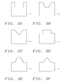
- FIGS. 3A through 3F are top-view representations of preferred embodiments of the special active regions of the present invention.
- FIGS. 4A through 4F are top-view representations of preferred embodiments of the plasma damage testing structure of the present invention.
- FIG. 5 is a cross-sectional representation of a gate structure to be simulated by the testing structure of the invention.
- FIG. 6 is a top-view of the gate structure to be simulated by the testing structure of the invention shown in cross-section in FIG. 5.
- FIG. 7 is a top view of a preferred embodiment of the testing structure of the present invention showing plasma damage.
- FIG. 1 there is illustrated a conventional plasma-damage testing structure of the prior art.
- Active area 10 is shown.
- Field oxide area 12 has been formed over the semiconductor substrate in the active area.
- Polysilicon gate 16 is shown within the active area.
- the gate oxide layer, not shown, underlies and is covered by the polysilicon gate 16 .
- FIG. 2 illustrates the degree of plasma-induced damage to the gate oxide shown across the top of the figure where no damage occurs to the left of line 22 .
- Increasing damage is shown to the right of line 22 in the direction of the arrow 24 .
- Slight damage occurs immediately to the right of line 22 .
- a testing structure of the prior art such as that shown in FIG. 1, there is a large “blind spot” 26 where damage occurs, but is not revealed by the testing structure. Greater damage to the right of the blind spot 26 can be caught by the testing structure.
- the testing structure of the present invention there is only a small blind spot 28 . Damage to the right of the blind spot 28 is revealed by the testing structure of the invention.
- the invention provides a more sensitive testing structure. Slight plasma damage that cannot be detected by the old method can be detected with the new method. This model allows an accurate evaluation of plasma/charging damage of actual MOSFET's for the future VLSI era.
- FIGS. 3A through 3F illustrate top views of various possible configurations of the special active region patterns of the invention.
- the active area is defined, for example, by a silicon nitride hard mask.
- the area outside and surrounding the active area comprises field oxide.
- the special pattern is applied to the active region 30 .
- the special pattern consists of an indentation in or a protuberance from the rectangular part of the active area, as shown in FIGS. 3 A- 3 F.
- the active area has. sharp corners or edges. This pattern enhances the degree of plasma damage to the active region caused by the residual stress from the edges or corners of the active area.
- the active area patterns shown in FIGS. 3 A- 3 F have a rectangular shape in top view.
- An indentation is cut into or a protuberance is formed out of the rectangular part of the active area.
- the indentation may have a rectangular shape as shown in FIG. 3A, inwardly sloping sidewalls with a flat bottom as shown in FIG. 3B, or a V-shape as shown in FIG. 3C.
- the protuberance may have a rectangular shape as shown in FIG. 3D, outwardly sloping sidewalls with a flat top as shown in FIG. 3E, or an inverted V-shape as shown in FIG. 3F.
- Other shapes having sharp corners are possible.
- a gate oxide layer is formed over the active area.
- a conduction layer is deposited over the gate oxide layer.
- the conduction layer and gate oxide layer are patterned to form the gate pattern 32 on the active region, as shown in FIGS. 4 A- 4 F.
- the conduction layer may be polysilicon or a metal, for example.
- testing structures can now be used for both edge-intensive and area-intensive plasma-damage monitoring. Wafers having these testing structures are exposed to a plasma environment. During exposure to a plasma environment, electron charge punches through the gate oxide (underlying the gate 32 ) to the substrate. Thus, pinholes will be formed in the gate oxide due to the plasma charge. Next, electrical tests are performed to calculate the degree of plasma damage.
- FIGS. 5 and 6 illustrate a MOSFET to be modeled by the test structure of the invention.
- polysilicon gate 56 overlies a gate oxide layer 54 and a field oxide region 52 in and on a semiconductor substrate 50 .
- FIG. 5 shows the cross-section 5 - 5 of the top view shown in FIG. 6. Damage to the gate oxide layer 54 is often seen near the edge of the FOX region 52 as indicated by 58 in the two figures.
- FIG. 7 illustrates in top view the testing structure of the present invention to be used to monitor plasma damage for the structure of the MOSFET example shown in FIGS. 5 and 6.
- 30 is the active area pattern used in the testing structure.
- the active area pattern has sharp corners which will enhance the degree of plasma damage to the test structure.
- the dashed line 36 indicates the real active area shape of the MOSFET.
- 32 is the gate pattern comprising a conductive layer overlying a gate oxide layer.
- the x's 38 shown in FIG. 7 indicate weak points due to stress during field oxide formation. Even very slight damage to the gate oxide layer can be detected by the test structures of the invention.
- the process of the present invention applies a special active region pattern as a plasma damage sensor.
- This sensor will monitor plasma/charging damage earlier and more effectively than the prior art testing structures.
- the testing structures of the invention use an active region pattern having sharp corners that enhances the degree of plasma damage by the residual stress from the edges or corners of the active region. This allows slight damage that cannot be caught by the previous methods to be detected, allowing for an early response to plasma damage.
Landscapes
- Insulated Gate Type Field-Effect Transistor (AREA)
- Testing Or Measuring Of Semiconductors Or The Like (AREA)
Abstract
A method of early and effective detection of plasma damage to a gate oxide layer by a special design of the active region is achieved. A plasma-damage testing structure is fabricated by providing a gate electrode overlying an active area of a semiconductor substrate wherein a gate oxide layer underlies the gate electrode. A portion of the active area underlying the gate electrode has sharp corners. The plasma-damage testing structure is exposed to a plasma environment. Electrical tests are performed to detect plasma damage to the plasma-damage testing structure. This model provides an accurate evaluation of plasma damage to actual MOSFET's.
Description
- (1) Field of the Invention
- The present invention relates to the fabrication of integrated circuit devices, and more particularly, to a method of early detection of plasma/charging damage in the fabrication of integrated circuit devices.
- (2) Description of the Prior Art
- The manufacture of large scale integrated circuits involves hundreds of processing steps. Most of these processing steps involve depositing layers of material, patterning them by photolithographic techniques, and etching away the unwanted portions. Plasma etching processes are often used because they are dry processes and they provide the cleanliness and degree of control required in integrated circuit manufacture.
- The most important semiconductor device in current technology is the metal-oxide-silicon field effect transistor (MOSFET). This device consists of two shallow regions of one type semiconductor—the source and drain—seperated by a region of another type—the channel region. A gate electrode overlies the channel region and is separated from it by a thin gate oxide layer. This thin gate oxide layer is one of the most critical components of the MOSFET. Typically, the gate oxide layer is thermally grown silicon oxide having a thickness on the order of 70-150 Angstroms in the current 0.25 micron design rule. An insulating film this thin is highly susceptible to damage such as from ion and electron bombardment from plasmas during backend processing. Plasma-induced degradation of gate oxide reliability is a key issue in achieving high performance MOSFET's.
- The multiple exposures of gate oxides to steps involving plasmas has led to the emergence of several test structures designed to amplify the charging exposure and thereby allow proper and timely assessment of damage caused by the plasma processing steps. Plasma damage test structures are discussed in Silicon Processing for the VLSI Era, Vol. 3, by S. Wolf, Lattice Press, Sunset Beach, Calif. (1995) pp. 507-9. The conventional test structures fall into one of two categories: 1) antenna structures which have large areas of conductor exposed to plasma as compared to area of gate oxide, and 2) large area capacitors which are formed over the gate oxide. In addition, both types of structures may be either edge-intensive or area-intensive. However, it is difficult for these structures to catch plasma-induced damage in a timely manner if the damage is very slight.
- A number of patents have addressed the plasma-induced damage issue. U.S. Pat. No. 5,650,651 to Bui discloses a plasma damage reduction device. U.S. Pat. No. 5,781,445 describes a plasma damage test structure consisting of a MOSFET surrounded by a conductive shield grounded to the substrate. U.S. Pat. No. 5,596,207 to Krishnan et al discloses a modified MOS structure having conductive sidewalls over a gate used to test for plasma damage. U.S. Pat. No. 5,638,006 to Nariani et al teaches the use of a testing structure that can differentiate weak oxide from charge-damaged oxide using an antenna structure.
- Accordingly, it is a primary object of the invention to provide a reliable and very manufacturable method for detecting plasma damage to a gate oxide layer in the fabrication of integrated circuit devices.
- A further object of the invention is to provide a process for early and effective detection of plasma damage to a gate oxide layer.
- Another object is to provide a process for early and effective detection of plasma damage to a gate oxide layer by a special design of the active region.
- Yet another object is to provide a testing structure for early and effective detection of plasma damage to a gate oxide layer having a special design of the active region.
- In accordance with the objects of the invention, a method of early and effective detection of plasma damage to a gate oxide layer by a special design of the active region is achieved. A plasma-damage testing structure is fabricated by providing a gate electrode overlying an active area of a semiconductor substrate wherein a gate oxide layer underlies the gate electrode. A portion of the active area underlying the gate electrode has sharp corners. The plasma-damage testing structure is exposed to a plasma environment. Electrical tests are performed to detect plasma damage to the plasma-damage testing structure. This model provides an accurate evaluation of slight plasma damage to actual MOSFET's.
- In the accompanying drawings forming a material part of this description, there is shown:
- FIG. 1 is a top-view representation of a testing structure of the prior art.
- FIG. 2 is a representation of the difference in sensitivity of a prior art testing structure and the testing structure of the present invention.
- FIGS. 3A through 3F are top-view representations of preferred embodiments of the special active regions of the present invention.
- FIGS. 4A through 4F are top-view representations of preferred embodiments of the plasma damage testing structure of the present invention.
- FIG. 5 is a cross-sectional representation of a gate structure to be simulated by the testing structure of the invention.
- FIG. 6 is a top-view of the gate structure to be simulated by the testing structure of the invention shown in cross-section in FIG. 5.
- FIG. 7 is a top view of a preferred embodiment of the testing structure of the present invention showing plasma damage.
- Referring now to FIG. 1, there is illustrated a conventional plasma-damage testing structure of the prior art.
Active area 10 is shown.Field oxide area 12 has been formed over the semiconductor substrate in the active area. Polysilicongate 16 is shown within the active area. The gate oxide layer, not shown, underlies and is covered by thepolysilicon gate 16. - FIG. 2 illustrates the degree of plasma-induced damage to the gate oxide shown across the top of the figure where no damage occurs to the left of
line 22. Increasing damage is shown to the right ofline 22 in the direction of thearrow 24. Slight damage occurs immediately to the right ofline 22. With a testing structure of the prior art, such as that shown in FIG. 1, there is a large “blind spot” 26 where damage occurs, but is not revealed by the testing structure. Greater damage to the right of theblind spot 26 can be caught by the testing structure. - In contrast, with the testing structure of the present invention, there is only a small
blind spot 28. Damage to the right of theblind spot 28 is revealed by the testing structure of the invention. Thus, the invention provides a more sensitive testing structure. Slight plasma damage that cannot be detected by the old method can be detected with the new method. This model allows an accurate evaluation of plasma/charging damage of actual MOSFET's for the future VLSI era. - The process of the present invention for forming plasma-induced damage testing structures will now be described. FIGS. 3A through 3F illustrate top views of various possible configurations of the special active region patterns of the invention. The active area is defined, for example, by a silicon nitride hard mask. The area outside and surrounding the active area comprises field oxide.
- The special pattern is applied to the
active region 30. The special pattern consists of an indentation in or a protuberance from the rectangular part of the active area, as shown in FIGS. 3A-3F. Thus, the active area has. sharp corners or edges. This pattern enhances the degree of plasma damage to the active region caused by the residual stress from the edges or corners of the active area. - For example, the active area patterns shown in FIGS. 3A-3F have a rectangular shape in top view. An indentation is cut into or a protuberance is formed out of the rectangular part of the active area. The indentation may have a rectangular shape as shown in FIG. 3A, inwardly sloping sidewalls with a flat bottom as shown in FIG. 3B, or a V-shape as shown in FIG. 3C. The protuberance may have a rectangular shape as shown in FIG. 3D, outwardly sloping sidewalls with a flat top as shown in FIG. 3E, or an inverted V-shape as shown in FIG. 3F. Other shapes having sharp corners are possible.
- A gate oxide layer is formed over the active area. A conduction layer is deposited over the gate oxide layer. The conduction layer and gate oxide layer are patterned to form the
gate pattern 32 on the active region, as shown in FIGS. 4A-4F. The conduction layer may be polysilicon or a metal, for example. - These testing structures can now be used for both edge-intensive and area-intensive plasma-damage monitoring. Wafers having these testing structures are exposed to a plasma environment. During exposure to a plasma environment, electron charge punches through the gate oxide (underlying the gate 32) to the substrate. Thus, pinholes will be formed in the gate oxide due to the plasma charge. Next, electrical tests are performed to calculate the degree of plasma damage.
- For example, FIGS. 5 and 6 illustrate a MOSFET to be modeled by the test structure of the invention. In the figures,
polysilicon gate 56 overlies agate oxide layer 54 and afield oxide region 52 in and on asemiconductor substrate 50. FIG. 5 shows the cross-section 5-5 of the top view shown in FIG. 6. Damage to thegate oxide layer 54 is often seen near the edge of theFOX region 52 as indicated by 58 in the two figures. - FIG. 7 illustrates in top view the testing structure of the present invention to be used to monitor plasma damage for the structure of the MOSFET example shown in FIGS. 5 and 6. 30 is the active area pattern used in the testing structure. The active area pattern has sharp corners which will enhance the degree of plasma damage to the test structure. The dashed
line 36 indicates the real active area shape of the MOSFET. 32 is the gate pattern comprising a conductive layer overlying a gate oxide layer. The x's 38 shown in FIG. 7 indicate weak points due to stress during field oxide formation. Even very slight damage to the gate oxide layer can be detected by the test structures of the invention. - The process of the present invention applies a special active region pattern as a plasma damage sensor. This sensor will monitor plasma/charging damage earlier and more effectively than the prior art testing structures. The testing structures of the invention use an active region pattern having sharp corners that enhances the degree of plasma damage by the residual stress from the edges or corners of the active region. This allows slight damage that cannot be caught by the previous methods to be detected, allowing for an early response to plasma damage.
- While the invention has been particularly shown and described with reference to the preferred embodiments thereof, it will be understood by those skilled in the art that various changes in form and details may be made without departing from the spirit and scope of the invention.
Claims (20)
1. A method of forming a plasma-damage testing structure comprising:
providing a gate electrode overlying an active area of a semiconductor substrate wherein a gate oxide layer underlies said gate electrode and wherein a portion of said active area underlying said gate electrode has sharp corners to complete said plasma-damage testing structure wherein said plasma-damage testing structure will simulate plasma damage to said gate oxide layer in the fabrication of an integrated circuit device.
2. The method according to claim 1 wherein said sharp corners cause residual stress in said active area which enhances the degree of plasma damage to said active area.
3. The method according to claim 1 wherein said active area has a rectangular shape in top view having an indentation cut into said rectangular shape wherein said indentation has sharp corners.
4. The method according to claim 3 wherein said indentation has a rectangular shape in top view.
5. The method according to claim 3 wherein said indentation has a V-shape in top view.
6. The method according to claim 3 wherein said indentation has a shape having inward sloping sidewalls and a flat bottom in top view.
7. The method according to claim 1 wherein said active area has a rectangular shape in top view having an protuberance out of said rectangular shape wherein said protuberance has sharp corners.
8. The method according to claim 7 wherein said protuberance has a rectangular shape in top view.
9. The method according to claim 7 wherein said protuberance has an inverted V-shape in top view.
10. The method according to claim 7 wherein said protuberance has a shape having outward sloping sidewalls and a flat top in top view.
11. A method of detecting plasma damage comprising:
fabricating a plasma-damage testing structure comprising providing a gate electrode overlying an active area of a semiconductor substrate wherein a portion of said active area underlying said gate electrode has sharp corners;
exposing said plasma-damage testing structure to a plasma environment; and
performing electrical tests to detect plasma damage to said plasma-damage testing structure.
12. The method according to claim 11 wherein said sharp corners cause residual stress in said active area which enhances the degree of plasma damage to said active area.
13. The method according to claim 11 wherein said active area has a rectangular shape in top view having an indentation cut into said rectangular shape wherein said indentation has sharp corners.
14. The method according to claim 11 wherein aid active area has a rectangular shape in top view having an protuberance out of said rectangular shape wherein said protuberance has sharp corners.
15. A method of detecting plasma damage comprising:
fabricating a plasma-damage testing structure comprising providing a gate electrode overlying an active area of a semiconductor substrate wherein a gate oxide layer underlies said gate electrode and wherein a portion of said active area underlying said gate electrode has sharp corners;
exposing said plasma-damage testing structure to a plasma environment; and
performing electrical tests to detect plasma damage to said plasma-damage testing structure.
16. The method according to claim 15 wherein said sharp corners cause residual stress in said active area which enhances the degree of plasma damage to said gate oxide layer.
17. The method according to claim 15 wherein said active area has a rectangular shape in top view having an indentation cut into said rectangular shape wherein said indentation has sharp corners.
18. The method according to claim 15 wherein said active area has a rectangular shape in top view having an protuberance out of said rectangular shape wherein said protuberance has sharp corners.
19. A plasma-damage testing structure comprising:
a gate electrode overlying an active area of a semiconductor substrate wherein a gate oxide layer underlies said gate electrode and wherein a portion of said active area underlying said gate electrode has sharp corners.
20. The plasma-damage testing structure according to claim 19 wherein said plasma-damage testing structure will simulate plasma damage to said gate oxide layer in the fabrication of an integrated circuit device.
Priority Applications (1)
| Application Number | Priority Date | Filing Date | Title |
|---|---|---|---|
| US10/462,266 US6929965B2 (en) | 1999-07-16 | 2003-06-16 | Early response to plasma/charging damage by special pattern design of active region |
Applications Claiming Priority (2)
| Application Number | Priority Date | Filing Date | Title |
|---|---|---|---|
| US09/356,002 US6593157B1 (en) | 1999-07-16 | 1999-07-16 | Early response to plasma/charging damage by special pattern design of active region |
| US10/462,266 US6929965B2 (en) | 1999-07-16 | 2003-06-16 | Early response to plasma/charging damage by special pattern design of active region |
Related Parent Applications (1)
| Application Number | Title | Priority Date | Filing Date |
|---|---|---|---|
| US09/356,002 Division US6593157B1 (en) | 1999-07-16 | 1999-07-16 | Early response to plasma/charging damage by special pattern design of active region |
Publications (2)
| Publication Number | Publication Date |
|---|---|
| US20030194822A1 true US20030194822A1 (en) | 2003-10-16 |
| US6929965B2 US6929965B2 (en) | 2005-08-16 |
Family
ID=23399673
Family Applications (2)
| Application Number | Title | Priority Date | Filing Date |
|---|---|---|---|
| US09/356,002 Expired - Lifetime US6593157B1 (en) | 1999-07-16 | 1999-07-16 | Early response to plasma/charging damage by special pattern design of active region |
| US10/462,266 Expired - Fee Related US6929965B2 (en) | 1999-07-16 | 2003-06-16 | Early response to plasma/charging damage by special pattern design of active region |
Family Applications Before (1)
| Application Number | Title | Priority Date | Filing Date |
|---|---|---|---|
| US09/356,002 Expired - Lifetime US6593157B1 (en) | 1999-07-16 | 1999-07-16 | Early response to plasma/charging damage by special pattern design of active region |
Country Status (1)
| Country | Link |
|---|---|
| US (2) | US6593157B1 (en) |
Cited By (3)
| Publication number | Priority date | Publication date | Assignee | Title |
|---|---|---|---|---|
| US20080150072A1 (en) * | 2006-12-20 | 2008-06-26 | Winstead Brian A | Integrated circuit having tensile and compressive regions |
| US20080179679A1 (en) * | 2007-01-31 | 2008-07-31 | Freescale Semiconductor, Inc. | Electronic device including insulating layers having different strains and a process for forming the electronic device |
| US20080296633A1 (en) * | 2005-11-08 | 2008-12-04 | Freescale Semiconductor, Inc. | Electronic device including a transistor structure having an active region adjacent to a stressor layer |
Families Citing this family (7)
| Publication number | Priority date | Publication date | Assignee | Title |
|---|---|---|---|---|
| US7115951B1 (en) * | 2002-09-04 | 2006-10-03 | National Semiconductor Corporation | Low triggering voltage ESD protection structure and method for reducing the triggering voltage |
| KR100674935B1 (en) * | 2005-01-06 | 2007-01-26 | 삼성전자주식회사 | Gate layout of semiconductor devices |
| CN101697351B (en) * | 2009-09-25 | 2012-08-08 | 上海宏力半导体制造有限公司 | Structure for testing semiconductor |
| CN101800212B (en) * | 2010-03-12 | 2013-09-25 | 上海宏力半导体制造有限公司 | Test structure for integrity of semiconductor element gate oxide |
| CN101853843B (en) * | 2010-03-12 | 2015-03-18 | 上海华虹宏力半导体制造有限公司 | Structure for testing integrality of gate oxide of semiconductor part |
| CN101819941B (en) * | 2010-04-29 | 2014-03-12 | 上海宏力半导体制造有限公司 | Testing structure of integrity of semiconductor device gate oxide |
| US9228025B2 (en) | 2012-03-12 | 2016-01-05 | Empire Technology Development Llc | Chicken antibodies that bind to nanoparticles |
Citations (8)
| Publication number | Priority date | Publication date | Assignee | Title |
|---|---|---|---|---|
| US5596207A (en) * | 1994-04-08 | 1997-01-21 | Texas Instruments Incorporated | Apparatus and method for detecting defects in insulative layers of MOS active devices |
| US5638006A (en) * | 1995-01-20 | 1997-06-10 | Vlsi Technology, Inc. | Method and apparatus for wafer level prediction of thin oxide reliability using differentially sized gate-like antennae |
| US5650651A (en) * | 1994-11-15 | 1997-07-22 | Advanced Micro Devices, Inc. | Plasma damage reduction device for sub-half micron technology |
| US5781445A (en) * | 1996-08-22 | 1998-07-14 | Taiwan Semiconductor Manufacturing Company, Ltd. | Plasma damage monitor |
| US5886363A (en) * | 1994-03-17 | 1999-03-23 | Fujitsu Limited | Semiconductor device and pattern including varying transistor patterns for evaluating characteristics |
| US6005266A (en) * | 1997-03-13 | 1999-12-21 | The Trustees Of Princeton University | Very low leakage JFET for monolithically integrated arrays |
| US6150669A (en) * | 1998-12-18 | 2000-11-21 | Texas Instruments Incorporated | Combination test structures for in-situ measurements during fabrication of semiconductor devices |
| US6175140B1 (en) * | 1996-08-23 | 2001-01-16 | Kabushiki Kaisha Toshiba | Semiconductor device using a shallow trench isolation |
-
1999
- 1999-07-16 US US09/356,002 patent/US6593157B1/en not_active Expired - Lifetime
-
2003
- 2003-06-16 US US10/462,266 patent/US6929965B2/en not_active Expired - Fee Related
Patent Citations (8)
| Publication number | Priority date | Publication date | Assignee | Title |
|---|---|---|---|---|
| US5886363A (en) * | 1994-03-17 | 1999-03-23 | Fujitsu Limited | Semiconductor device and pattern including varying transistor patterns for evaluating characteristics |
| US5596207A (en) * | 1994-04-08 | 1997-01-21 | Texas Instruments Incorporated | Apparatus and method for detecting defects in insulative layers of MOS active devices |
| US5650651A (en) * | 1994-11-15 | 1997-07-22 | Advanced Micro Devices, Inc. | Plasma damage reduction device for sub-half micron technology |
| US5638006A (en) * | 1995-01-20 | 1997-06-10 | Vlsi Technology, Inc. | Method and apparatus for wafer level prediction of thin oxide reliability using differentially sized gate-like antennae |
| US5781445A (en) * | 1996-08-22 | 1998-07-14 | Taiwan Semiconductor Manufacturing Company, Ltd. | Plasma damage monitor |
| US6175140B1 (en) * | 1996-08-23 | 2001-01-16 | Kabushiki Kaisha Toshiba | Semiconductor device using a shallow trench isolation |
| US6005266A (en) * | 1997-03-13 | 1999-12-21 | The Trustees Of Princeton University | Very low leakage JFET for monolithically integrated arrays |
| US6150669A (en) * | 1998-12-18 | 2000-11-21 | Texas Instruments Incorporated | Combination test structures for in-situ measurements during fabrication of semiconductor devices |
Cited By (7)
| Publication number | Priority date | Publication date | Assignee | Title |
|---|---|---|---|---|
| US20080296633A1 (en) * | 2005-11-08 | 2008-12-04 | Freescale Semiconductor, Inc. | Electronic device including a transistor structure having an active region adjacent to a stressor layer |
| US7714318B2 (en) * | 2005-11-08 | 2010-05-11 | Freescale Semiconductor, Inc | Electronic device including a transistor structure having an active region adjacent to a stressor layer |
| US20080150072A1 (en) * | 2006-12-20 | 2008-06-26 | Winstead Brian A | Integrated circuit having tensile and compressive regions |
| US8569858B2 (en) | 2006-12-20 | 2013-10-29 | Freescale Semiconductor, Inc. | Semiconductor device including an active region and two layers having different stress characteristics |
| US9847389B2 (en) | 2006-12-20 | 2017-12-19 | Nxp Usa, Inc. | Semiconductor device including an active region and two layers having different stress characteristics |
| US20080179679A1 (en) * | 2007-01-31 | 2008-07-31 | Freescale Semiconductor, Inc. | Electronic device including insulating layers having different strains and a process for forming the electronic device |
| US7843011B2 (en) | 2007-01-31 | 2010-11-30 | Freescale Semiconductor, Inc. | Electronic device including insulating layers having different strains |
Also Published As
| Publication number | Publication date |
|---|---|
| US6593157B1 (en) | 2003-07-15 |
| US6929965B2 (en) | 2005-08-16 |
Similar Documents
| Publication | Publication Date | Title |
|---|---|---|
| US6673636B2 (en) | Method of real-time plasma charging voltage measurement on powered electrode with electrostatic chuck in plasma process chambers | |
| US20050026310A1 (en) | Method for in-line monitoring of via/contact holes etch process based on test structures in semiconductor wafer manufacturing | |
| US6586765B2 (en) | Wafer-level antenna effect detection pattern for VLSI | |
| US5869877A (en) | Methods and apparatus for detecting pattern dependent charging on a workpiece in a plasma processing system | |
| US5596207A (en) | Apparatus and method for detecting defects in insulative layers of MOS active devices | |
| US6593157B1 (en) | Early response to plasma/charging damage by special pattern design of active region | |
| CN101114634B (en) | Test structure and method for detecting charge effects in semiconductor processing | |
| JPH02270342A (en) | Manufacture of semiconductor device | |
| US7474001B2 (en) | Method for in-line monitoring of via/contact holes etch process based on test structures in semiconductor wafer manufacturing | |
| JP5276926B2 (en) | Contact hole side wall resistance measurement method | |
| US6274396B1 (en) | Method of manufacturing calibration wafers for determining in-line defect scan tool sensitivity | |
| JPH08298237A (en) | Semiconductor device having superposition measuring mark and manufacture thereof | |
| CN100403508C (en) | Defect detecting element and method for detecting and manufacturing the same | |
| TWI292601B (en) | Defect inspection device and inspecting method thereof | |
| JP3151791B2 (en) | Monitor pattern of critical dimension control device and method of using the same | |
| US6677608B2 (en) | Semiconductor device for detecting gate defects | |
| KR100531952B1 (en) | A monitoring pattern of Shallow Trench Isolation profile | |
| JPH1079407A (en) | Dry etching damage detection device and semiconductor device diagnosis method | |
| JP3341694B2 (en) | Inspection method of plasma damage and its inspection element | |
| JP3249218B2 (en) | How to detect resist scum | |
| JP2004031859A (en) | Semiconductor device and manufacturing method thereof | |
| JP3332022B2 (en) | Semiconductor device damage evaluation method | |
| KR20000056067A (en) | Method for forming semiconductor device antenna pattern for monitoring plasma damage | |
| JPH09139459A (en) | Conductive device structure capable of being rendered non-conductive by an etching process | |
| KR100261178B1 (en) | Method for improving sensitivity of find target |
Legal Events
| Date | Code | Title | Description |
|---|---|---|---|
| FPAY | Fee payment |
Year of fee payment: 4 |
|
| FPAY | Fee payment |
Year of fee payment: 8 |
|
| REMI | Maintenance fee reminder mailed | ||
| LAPS | Lapse for failure to pay maintenance fees |
Free format text: PATENT EXPIRED FOR FAILURE TO PAY MAINTENANCE FEES (ORIGINAL EVENT CODE: EXP.) |
|
| STCH | Information on status: patent discontinuation |
Free format text: PATENT EXPIRED DUE TO NONPAYMENT OF MAINTENANCE FEES UNDER 37 CFR 1.362 |
|
| FP | Lapsed due to failure to pay maintenance fee |
Effective date: 20170816 |