US11738411B2 - Lead-free solder paste with mixed solder powders for high temperature applications - Google Patents
Lead-free solder paste with mixed solder powders for high temperature applications Download PDFInfo
- Publication number
- US11738411B2 US11738411B2 US17/244,141 US202117244141A US11738411B2 US 11738411 B2 US11738411 B2 US 11738411B2 US 202117244141 A US202117244141 A US 202117244141A US 11738411 B2 US11738411 B2 US 11738411B2
- Authority
- US
- United States
- Prior art keywords
- solder
- alloy powder
- solder alloy
- paste
- solder paste
- Prior art date
- Legal status (The legal status is an assumption and is not a legal conclusion. Google has not performed a legal analysis and makes no representation as to the accuracy of the status listed.)
- Active, expires
Links
Images




Classifications
-
- B—PERFORMING OPERATIONS; TRANSPORTING
- B23—MACHINE TOOLS; METAL-WORKING NOT OTHERWISE PROVIDED FOR
- B23K—SOLDERING OR UNSOLDERING; WELDING; CLADDING OR PLATING BY SOLDERING OR WELDING; CUTTING BY APPLYING HEAT LOCALLY, e.g. FLAME CUTTING; WORKING BY LASER BEAM
- B23K35/00—Rods, electrodes, materials, or media, for use in soldering, welding, or cutting
- B23K35/22—Rods, electrodes, materials, or media, for use in soldering, welding, or cutting characterised by the composition or nature of the material
- B23K35/24—Selection of soldering or welding materials proper
- B23K35/26—Selection of soldering or welding materials proper with the principal constituent melting at less than 400°C
- B23K35/262—Sn as the principal constituent
-
- B—PERFORMING OPERATIONS; TRANSPORTING
- B23—MACHINE TOOLS; METAL-WORKING NOT OTHERWISE PROVIDED FOR
- B23K—SOLDERING OR UNSOLDERING; WELDING; CLADDING OR PLATING BY SOLDERING OR WELDING; CUTTING BY APPLYING HEAT LOCALLY, e.g. FLAME CUTTING; WORKING BY LASER BEAM
- B23K1/00—Soldering, e.g. brazing, or unsoldering
- B23K1/20—Preliminary treatment of work or areas to be soldered, e.g. in respect of a galvanic coating
- B23K1/203—Fluxing, i.e. applying flux onto surfaces
-
- B—PERFORMING OPERATIONS; TRANSPORTING
- B23—MACHINE TOOLS; METAL-WORKING NOT OTHERWISE PROVIDED FOR
- B23K—SOLDERING OR UNSOLDERING; WELDING; CLADDING OR PLATING BY SOLDERING OR WELDING; CUTTING BY APPLYING HEAT LOCALLY, e.g. FLAME CUTTING; WORKING BY LASER BEAM
- B23K35/00—Rods, electrodes, materials, or media, for use in soldering, welding, or cutting
- B23K35/02—Rods, electrodes, materials, or media, for use in soldering, welding, or cutting characterised by mechanical features, e.g. shape
- B23K35/0222—Rods, electrodes, materials, or media, for use in soldering, welding, or cutting characterised by mechanical features, e.g. shape for use in soldering or brazing
- B23K35/0244—Powders, particles or spheres; Preforms made therefrom
- B23K35/025—Pastes, creams or slurries
-
- B—PERFORMING OPERATIONS; TRANSPORTING
- B23—MACHINE TOOLS; METAL-WORKING NOT OTHERWISE PROVIDED FOR
- B23K—SOLDERING OR UNSOLDERING; WELDING; CLADDING OR PLATING BY SOLDERING OR WELDING; CUTTING BY APPLYING HEAT LOCALLY, e.g. FLAME CUTTING; WORKING BY LASER BEAM
- B23K35/00—Rods, electrodes, materials, or media, for use in soldering, welding, or cutting
- B23K35/22—Rods, electrodes, materials, or media, for use in soldering, welding, or cutting characterised by the composition or nature of the material
- B23K35/24—Selection of soldering or welding materials proper
- B23K35/26—Selection of soldering or welding materials proper with the principal constituent melting at less than 400°C
-
- B—PERFORMING OPERATIONS; TRANSPORTING
- B23—MACHINE TOOLS; METAL-WORKING NOT OTHERWISE PROVIDED FOR
- B23K—SOLDERING OR UNSOLDERING; WELDING; CLADDING OR PLATING BY SOLDERING OR WELDING; CUTTING BY APPLYING HEAT LOCALLY, e.g. FLAME CUTTING; WORKING BY LASER BEAM
- B23K35/00—Rods, electrodes, materials, or media, for use in soldering, welding, or cutting
- B23K35/22—Rods, electrodes, materials, or media, for use in soldering, welding, or cutting characterised by the composition or nature of the material
- B23K35/36—Selection of non-metallic compositions, e.g. coatings or fluxes; Selection of soldering or welding materials, conjoint with selection of non-metallic compositions, both selections being of interest
- B23K35/362—Selection of compositions of fluxes
-
- C—CHEMISTRY; METALLURGY
- C22—METALLURGY; FERROUS OR NON-FERROUS ALLOYS; TREATMENT OF ALLOYS OR NON-FERROUS METALS
- C22C—ALLOYS
- C22C12/00—Alloys based on antimony or bismuth
-
- C—CHEMISTRY; METALLURGY
- C22—METALLURGY; FERROUS OR NON-FERROUS ALLOYS; TREATMENT OF ALLOYS OR NON-FERROUS METALS
- C22C—ALLOYS
- C22C13/00—Alloys based on tin
-
- C—CHEMISTRY; METALLURGY
- C22—METALLURGY; FERROUS OR NON-FERROUS ALLOYS; TREATMENT OF ALLOYS OR NON-FERROUS METALS
- C22C—ALLOYS
- C22C13/00—Alloys based on tin
- C22C13/02—Alloys based on tin with antimony or bismuth as the next major constituent
-
- H—ELECTRICITY
- H10—SEMICONDUCTOR DEVICES; ELECTRIC SOLID-STATE DEVICES NOT OTHERWISE PROVIDED FOR
- H10W—GENERIC PACKAGES, INTERCONNECTIONS, CONNECTORS OR OTHER CONSTRUCTIONAL DETAILS OF DEVICES COVERED BY CLASS H10
- H10W70/00—Package substrates; Interposers; Redistribution layers [RDL]
- H10W70/40—Leadframes
- H10W70/411—Chip-supporting parts, e.g. die pads
- H10W70/417—Bonding materials between chips and die pads
-
- B—PERFORMING OPERATIONS; TRANSPORTING
- B23—MACHINE TOOLS; METAL-WORKING NOT OTHERWISE PROVIDED FOR
- B23K—SOLDERING OR UNSOLDERING; WELDING; CLADDING OR PLATING BY SOLDERING OR WELDING; CUTTING BY APPLYING HEAT LOCALLY, e.g. FLAME CUTTING; WORKING BY LASER BEAM
- B23K2103/00—Materials to be soldered, welded or cut
- B23K2103/08—Non-ferrous metals or alloys
-
- H—ELECTRICITY
- H10—SEMICONDUCTOR DEVICES; ELECTRIC SOLID-STATE DEVICES NOT OTHERWISE PROVIDED FOR
- H10W—GENERIC PACKAGES, INTERCONNECTIONS, CONNECTORS OR OTHER CONSTRUCTIONAL DETAILS OF DEVICES COVERED BY CLASS H10
- H10W72/00—Interconnections or connectors in packages
- H10W72/071—Connecting or disconnecting
- H10W72/073—Connecting or disconnecting of die-attach connectors
- H10W72/07331—Connecting techniques
- H10W72/07336—Soldering or alloying
-
- H—ELECTRICITY
- H10—SEMICONDUCTOR DEVICES; ELECTRIC SOLID-STATE DEVICES NOT OTHERWISE PROVIDED FOR
- H10W—GENERIC PACKAGES, INTERCONNECTIONS, CONNECTORS OR OTHER CONSTRUCTIONAL DETAILS OF DEVICES COVERED BY CLASS H10
- H10W72/00—Interconnections or connectors in packages
- H10W72/071—Connecting or disconnecting
- H10W72/073—Connecting or disconnecting of die-attach connectors
- H10W72/07351—Connecting or disconnecting of die-attach connectors characterised by changes in properties of the die-attach connectors during connecting
- H10W72/07355—Connecting or disconnecting of die-attach connectors characterised by changes in properties of the die-attach connectors during connecting changes in materials
-
- H—ELECTRICITY
- H10—SEMICONDUCTOR DEVICES; ELECTRIC SOLID-STATE DEVICES NOT OTHERWISE PROVIDED FOR
- H10W—GENERIC PACKAGES, INTERCONNECTIONS, CONNECTORS OR OTHER CONSTRUCTIONAL DETAILS OF DEVICES COVERED BY CLASS H10
- H10W72/00—Interconnections or connectors in packages
- H10W72/30—Die-attach connectors
- H10W72/321—Structures or relative sizes of die-attach connectors
- H10W72/325—Die-attach connectors having a filler embedded in a matrix
-
- H—ELECTRICITY
- H10—SEMICONDUCTOR DEVICES; ELECTRIC SOLID-STATE DEVICES NOT OTHERWISE PROVIDED FOR
- H10W—GENERIC PACKAGES, INTERCONNECTIONS, CONNECTORS OR OTHER CONSTRUCTIONAL DETAILS OF DEVICES COVERED BY CLASS H10
- H10W72/00—Interconnections or connectors in packages
- H10W72/30—Die-attach connectors
- H10W72/351—Materials of die-attach connectors
- H10W72/352—Materials of die-attach connectors comprising metals or metalloids, e.g. solders
-
- H—ELECTRICITY
- H10—SEMICONDUCTOR DEVICES; ELECTRIC SOLID-STATE DEVICES NOT OTHERWISE PROVIDED FOR
- H10W—GENERIC PACKAGES, INTERCONNECTIONS, CONNECTORS OR OTHER CONSTRUCTIONAL DETAILS OF DEVICES COVERED BY CLASS H10
- H10W72/00—Interconnections or connectors in packages
- H10W72/30—Die-attach connectors
- H10W72/351—Materials of die-attach connectors
- H10W72/352—Materials of die-attach connectors comprising metals or metalloids, e.g. solders
- H10W72/3528—Intermetallic compounds
-
- H—ELECTRICITY
- H10—SEMICONDUCTOR DEVICES; ELECTRIC SOLID-STATE DEVICES NOT OTHERWISE PROVIDED FOR
- H10W—GENERIC PACKAGES, INTERCONNECTIONS, CONNECTORS OR OTHER CONSTRUCTIONAL DETAILS OF DEVICES COVERED BY CLASS H10
- H10W72/00—Interconnections or connectors in packages
- H10W72/30—Die-attach connectors
- H10W72/351—Materials of die-attach connectors
- H10W72/353—Materials of die-attach connectors not comprising solid metals or solid metalloids, e.g. ceramics
-
- H—ELECTRICITY
- H10—SEMICONDUCTOR DEVICES; ELECTRIC SOLID-STATE DEVICES NOT OTHERWISE PROVIDED FOR
- H10W—GENERIC PACKAGES, INTERCONNECTIONS, CONNECTORS OR OTHER CONSTRUCTIONAL DETAILS OF DEVICES COVERED BY CLASS H10
- H10W72/00—Interconnections or connectors in packages
- H10W72/90—Bond pads, in general
- H10W72/951—Materials of bond pads
- H10W72/952—Materials of bond pads comprising metals or metalloids, e.g. PbSn, Ag or Cu
-
- H—ELECTRICITY
- H10—SEMICONDUCTOR DEVICES; ELECTRIC SOLID-STATE DEVICES NOT OTHERWISE PROVIDED FOR
- H10W—GENERIC PACKAGES, INTERCONNECTIONS, CONNECTORS OR OTHER CONSTRUCTIONAL DETAILS OF DEVICES COVERED BY CLASS H10
- H10W90/00—Package configurations
- H10W90/701—Package configurations characterised by the relative positions of pads or connectors relative to package parts
- H10W90/731—Package configurations characterised by the relative positions of pads or connectors relative to package parts of die-attach connectors
- H10W90/736—Package configurations characterised by the relative positions of pads or connectors relative to package parts of die-attach connectors between a chip and a stacked lead frame, conducting package substrate or heat sink
Definitions
- the present disclosure relates to lead-free solder pastes.
- a common use of high melting temperature solders is die-attachment for semiconductor surface mounting devices/components in which the chip will be bonded between leads or onto a lead frame. These surface mounting components/devices are then used in one or more subsequent board-level soldering processes. For example, a silicon die is soldered onto a lead-frame using a high melting temperature solder to form an assembly. Subsequently, the device (either encapsulated or not), is attached onto a printed wiring board (PWB) by a board-level reflow. The same board may be exposed to multiple reflows. During the whole process, the internal connection between the silicon die and the lead-frame should be well maintained. This requires that the high melting temperature solder resist multiple reflow soldering processes without causing any functional failures.
- PWB printed wiring board
- Transient liquid phase bonding (TLPB) technology is aimed at achieving a higher remelting temperature of a solder joint through the formation of intermetallic compounds (IMCs) between low melting temperature alloys and high melting temperatures alloys.
- IMCs intermetallic compounds
- the low melting phase is mostly or even completely consumed during reflow to reach the high melting temperature target.
- the interfacial IMC formation on the surface of the high melting alloys and the continuous IMC growth come at the expense of both low melting alloys and high melting alloys during the reflow.
- Some implementations of the disclosure are directed to a lead-free solder paste with mixed solder powders that is particularly suitable for high temperature soldering applications involving multiple board-level reflow operations.
- a solder paste consists of: 10 wt % to 90 wt % of a first solder alloy powder, the first solder alloy powder consisting of an SnSbCuAg solder alloy that has a wt % ratio of Sn:Sb of 0.75 to 1.1; 10 wt % to 90 wt % of a second solder alloy powder, the second solder alloy powder consisting of an Sn solder alloy including at least 80 wt % of Sn; and a remainder of flux.
- the solder paste consists of 50 wt % to 90 wt % of the first solder alloy powder, 10 wt % to 50 wt % of the second solder alloy powder, and a remainder of the flux. In some implementations, the solder paste consists of 75 wt % to 90 wt % of the first solder alloy powder, 10 wt % to 25 wt % of the second solder alloy powder, and a remainder of the flux.
- the solder paste consists of less than 50 wt % of the first solder alloy powder, greater than 50 wt % of the second solder alloy powder, and a remainder of the flux.
- the solidus temperature of the first solder alloy powder is 300° C. to 360° C.
- the solidus temperature of the second solder alloy powder is 200° C. to 250° C.
- the solidus temperature of the second solder alloy powder is 215° C. to 245° C.
- the liquidus temperature of the first solder alloy powder is no greater than 360° C.
- the liquidus temperature of the second solder alloy powder is no greater than 250° C.
- the liquidus temperature of the second solder alloy powder is no greater than 245° C.
- the first solder alloy powder consists of: 4 wt % to 10 wt % of Cu; 4 wt % to 20 wt % of Ag; optionally, 0.5 wt % or less of Bi, Co, In, Ge, Ni, P, or Zn; and a remainder of Sn and Sb in the ratio of 0.75 to 1.1.
- the second solder alloy powder comprises 0.1 to 4 wt % Ag, 0.1 to 1 wt % Cu, or 0.1 to 11 wt % Sb. In some implementations, the second solder alloy powder comprises 0.1 to 4 wt % Ag, 0.1 to 1 wt % Cu, and 0.1 to 11 wt % Sb.
- the second solder alloy powder is doped with Bi, Co, Ge, In, Ni, P, Sb, or Zn.
- a ratio of heat absorption from a first melting peak of the solder paste to heat absorption from a second melting peak of the solder paste is 0.15 or less.
- a method comprises: applying a solder paste between a substrate and device to form an assembly, wherein the solder paste consists of: 10 wt % to 90 wt % of a first solder alloy powder, the first solder alloy powder consisting of an SnSbCuAg solder alloy that has a wt % ratio of Sn:Sb of 0.75 to 1.1; 10 wt % to 90 wt % of a second solder alloy powder, the second solder alloy powder consisting of an Sn solder alloy including at least 80 wt % of Sn; and a remainder of flux; performing a first reflow soldering process with the assembly at a peak temperature of greater than 320° C.
- the device is a silicon die
- the substrate comprises a Cu lead frame
- the solder paste is applied between the Cu lead frame and the silicon die.
- the solder joint maintains a bond shear strength greater than or equal to 10 MPa during the second reflow soldering process.
- a solder joint is formed by the process of: applying a solder paste between a substrate and a device to form an assembly; and reflow soldering the assembly to form the solder joint; wherein the solder paste consists of: 10 wt % to 90 wt % of a first solder alloy powder, the first solder alloy powder consisting of an SnSbCuAg solder alloy that has a wt % ratio of Sn:Sb of 0.75 to 1.1; 10 wt % to 90 wt % of a second solder alloy powder, the second solder alloy powder consisting of an Sn solder alloy including at least 80 wt % of Sn; and a remainder of flux.
- FIG. 1 is a chart showing bond shear strength in MPa as a function of temperature for several lead-free bonding materials and high-lead solders.
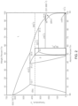
- FIG. 2 depicts a phase diagram of SnSb.
- FIG. 3 is a chart plot showing the bond shear strength in MPa for different testing temperatures (° C.) for five different solder pastes.
- FIG. 4 shows Differential Scanning calorimeter (DSC) heating curves performed with TA Q2000 DSC for the five solder pastes depicted in FIG. 3 .
- high temperature solders may include: (i) a solidus temperature of around 260° C. and above (in accordance with typical SMT solder reflow profiles), (ii) good thermal fatigue resistance, (iii) high thermal/electric conductivity, and/or (iv) low cost. To date, solders with a high lead content still dominate die-attachment applications in the power discrete market.
- Implementations of the disclosure are directed to a lead-free solder paste with mixed solder powders that is particularly suitable for high temperature soldering applications involving multiple board-level reflow operations.
- the solder paste comprises two solder powders and flux.
- One of the solder powders has a substantially higher melting temperature than the other solder powder.
- one of the solder powders may have a solidus temperature of a first solder alloy that is from 300 to 360° C.
- the other of the solder powders may have a solidus temperature of a second solder alloy from 200 to 250° C.
- the higher solidus temperature (higher temperature) solder powder is an SnSb-based solder alloy having an Sn:Sb weight ratio between about 0.75 and 1.1.
- the lower solidus temperature (lower temperature) solder powder is an Sn-rich solder or solder alloy with an Sn content greater than 80% by weight.
- the higher temperature solder powder comprises 50 wt % to 90 wt % of the solder paste
- the lower temperature solder powder comprises 10 wt % to 50 wt % of the solder paste
- the flux comprises 9 wt % to 20 wt % of the solder paste.
- the higher temperature solder powder may dominate the high temperature performance of the final bonding joint, including the melting and the thermo-mechanical behavior.
- the ductile Sn-rich solder powder may improve wetting during reflow and enhance the ductility of the final joint. Additionally, the existence of the Sn-rich solder inside the paste may permit a relatively lower reflow temperature.
- the selection of the lower temperature solder powder and the higher melting temperature solder powder in the solder paste may be made to satisfy one or more of the following properties: (1) the solder powders completely or partially dissolve into each other during the reflow process; 2) after reflow soldering, the remaining low melting phase in the final joint is optimized in quantity and isolated by the high melting SnSb matrix to maintain a desired joint mechanical performance at a temperature above 270° C.; and (3) the solder joint is able to survive a temperature cycle test for typical die attachment applications.
- both solder alloy powders may thoroughly or partially dissolve in to each other during reflow.
- the ratio of the lower temperature alloy powder and the higher temperature alloy powder may be optimized to allow the higher temperature alloy powder to dominate the high temperature performance of the final joint while the low melting phases are isolated inside the high melting phase matrix.
- solder pastes described herein may be used for a variety of high temperature soldering applications, including die attachment and surface mounting of components devices.
- FIG. 1 is a chart showing bond shear strength in megapascal (MPa) as a function of temperature for joints formed from several lead-free bonding materials and high-lead solders. As depicted, most of the lead-free solders have higher bond shear strength than the high-lead ones. Sn-rich solders significantly drop in bond shear strength when approaching the melting temperature of the solder (about 217° C. for SnAgCu and 243° C. for Sn10Sb). After reaching the melting temperature, the bond shear strength of the Sn-rich solders drops close to zero as they become molten. As such, because of the lower melting temperatures of Sn-rich solders, they may not be able to maintain any bond shear strength at high melting temperatures.
- MPa megapascal
- the high lead solders have a bond shear strength around 10 Mpa at 250° C., and the bond shear strength drops even lower at higher temperatures.
- Surface mounting devices with high lead solders as the die attach materials have been proven to survive subsequent SMT reflows at up to 260° C. peak temperatures.
- the novel solder pastes described herein are designed to maintain a bond shear strength above 10 MPa even at a temperature of 270° C. or higher, superior to high lead counterparts, to survive the following SMT process.
- SnSbCuAgX solders will cause the Si die to break during temperature cycling tests, or even right after reflow because they are too rigid to accommodate the strain caused by the coefficient of thermal expansion (CTE) mismatch between Si and Cu. Therefore, SnSbCuAgX solder alloys, by themselves, are not suitable for die attachment in die attach applications.
- solder paste that is a combination of a Sn-rich solder alloy powder, a SnSbCuAgX solder alloy powder, and a flux.
- the solder paste described herein may be reflowed to form a solder joint.
- the reflowed solder joint may demonstrate the benefits of both solder alloys: the ductility of Sn-rich alloys and the high temperature performance of SnSbCuAgX solder alloys.
- the ratio of the Sn-rich powder to the SnSbCuAgX powder may be chosen such that final joint exhibits (1) good mechanical strength (>10 MPa) at 270° C. or even higher; (2) and good ductility to accommodate the strain caused by the CTE mismatch between the Si die and Cu.
- the solder joint may be formed with a morphology that the Sn-rich phase of the low temperature solder alloy is embedded in the SnSb matrix of the high temperature solder alloy, similar to composite materials.
- the Sn-rich phase isolated inside the SnSb matrix may not significantly impact the high temperature strength of the solder joint because the majority of the solder joint is the SnSb matrix and the reinforced Cu-containing and Ag-containing particles.
- the ductile Sn-rich phase may easily deform through creep to accommodate the strain caused by the CTE mismatch between the Si die and the Cu lead frame at least partially.
- the higher temperature solder alloy may dominate high melting temperature performance at about 270° C. and above.
- the ratio between Sn and Sb in the higher temperature solder alloy may be maintained at about 0.75 to 1.1, in which a Sn3Sb2 intermetallic compound and SnSb solid solution ( ⁇ ) are formed and have a melting temperature between about 323° C. and 360° C. This is depicted by the phase SnSb phase diagram of FIG. 2 .
- the solidus temperature of the solder alloy may be maintained around 300° C. depending on the content. Accordingly, in some implementations, it is preferable that the high melting temperature solder alloy has about 4 wt % to 10 wt % Cu and about 4 wt % to 20 wt % Ag.
- Table 1 below shows examples of SnSbCuAg alloys that may be utilized for the higher temperature solder alloy, in accordance with implementations of the disclosure.
- dopants such as Bi, Co, In, Ge, Ni, P, or Zn, may be added to the SnSbCuAg solder alloy to stabilize the precipitates and the interfacial IMC.
- the lower melting temperature solder alloy may be an Sn-rich solder alloy (Sn>80 wt %).
- the solidus temperature of the lower temperature solder alloy may range from about 200° C. to 250° C.
- Table 2 below shows examples of Sn-rich alloys that may be utilized for the lower temperature solder alloy, in accordance with implementations of the disclosure.
- additives of Bi, In, and/or Ni may be included in the solder alloy to enhance its ductility or improve wetting performance.
- the higher temperature solder powder may comprise 10 wt % to 90 wt % of the solder paste
- the lower temperature solder powder comprises 10 wt % to 90 wt % of the solder paste.
- the ratio of first solder alloy and the second solder alloy may be tuned. If the wt % of the first solder alloy relative to the second solder alloy is insufficient, the final solder joint may not maintain high temperature performance. On the other hand, if the wt % of the first solder alloy relative to the second solder alloy is more than enough, the solder joint may be too rigid and result in the damage to the Si die.
- the relative ratios of the first solder alloy and the second solder alloy in the paste may be chosen such that both high temperature performance and sufficient ductility may be satisfied.
- the higher temperature solder powder may more preferably comprise 50 wt % to 90 wt % of the solder paste, and the lower temperature solder powder may comprise 10 wt % to 50 wt % of the solder paste.
- the higher temperature solder powder may more preferably comprise 75 wt % to 90 wt % of the solder paste, and the lower temperature solder powder may comprise 10 wt % to 25 wt % of the solder paste.
- the lower temperature solder powder may comprise greater than 50 wt % of the solder paste.
- Such implementations of the solder paste may be particularly suitable for power module applications that do not necessarily require high temperature strength.
- Table 3 shows the solder alloy elemental composition (in wt %) and reflow soldered joint solder elemental composition (in wt %) of solder pastes in accordance with the disclosure.
- the solder pastes may be utilized for HTLF (high temperature lead-free) die attach applications, or other suitable high temperature soldering applications.
- the ratio of the first solder alloy to the second solder alloy may range from about 9:1 to 5:5.
- the ratio of Sn:Sb in a solder joint formed from the solder paste may be around 1:1 to 1.3:1. In some implementations involving use of the solder paste in power module devices/applications, the ratio of Sn:Sb in a solder joint formed from the solder paste may be around 1:1 to 1.8:1.
- FIG. 3 is a chart plot showing the bond shear strength (MPa) for different testing temperatures (° C.) for solder joints formed from five different solder pastes. Specifically, FIG. 3 shows the bond shear strength for the first five solder pastes of Table 3, where 874-33-1 refers to the first solder paste in Table 1, 847-33-2 refers to the second solder paste in Table 3, etc. As depicted, three out of five solder pastes (874-33-1, 874-33-2 and 874-33-3) maintained a bond shear strength of at least 10 MPa at 270° C. and above.
- MPa bond shear strength
- FIG. 4 shows Differential Scanning calorimeter (DSC) heating curves measured with TA Q2000 DSC for the five solder pastes depicted in FIG. 3 .
- DSC Differential Scanning calorimeter
- a more preferable ratio of heat absorption from the first melting peak of the solder paste to heat absorption from the second melting peak of the solder paste was found to be about 0.15 or less. At these ratios, it was found that a joint formed from the solder paste can maintain sufficient high temperature shear strength (>15 MPa even at 280° C.) (e.g., from having a sufficient amount of the higher melting temperature solder powder) and good ductility (e.g., from having a sufficient amount of the Sn-rich powder).
- the selection of solder powders and the relative wt. % of the solder powders may be based on the H1/H2 ratio.
- implementations described herein do not rely on increasing the melting temperature of the solder joint via the formation of IMCs on the surface of high melting alloys by consuming low melting alloys.
- the IMC forms and grows on the surface of the high melting metal/alloy powders at the expense of the low melting alloys during reflow. With increasing IMC layer thickness, the growth rate becomes significantly slower.
- solder joints formed by the solder pastes described herein are not dependent on the formation of IMCs during reflow to achieve high temperature performance. Rather, high temperature performance may be obtained by selecting the appropriate percentage of the high melting phases in the final joint and by confining the low melting phases with the high melting phases after solidification.
Landscapes
- Engineering & Computer Science (AREA)
- Mechanical Engineering (AREA)
- Chemical & Material Sciences (AREA)
- Materials Engineering (AREA)
- Metallurgy (AREA)
- Organic Chemistry (AREA)
- Electric Connection Of Electric Components To Printed Circuits (AREA)
- Die Bonding (AREA)
Priority Applications (1)
| Application Number | Priority Date | Filing Date | Title |
|---|---|---|---|
| US17/244,141 US11738411B2 (en) | 2020-04-29 | 2021-04-29 | Lead-free solder paste with mixed solder powders for high temperature applications |
Applications Claiming Priority (2)
| Application Number | Priority Date | Filing Date | Title |
|---|---|---|---|
| US202063017469P | 2020-04-29 | 2020-04-29 | |
| US17/244,141 US11738411B2 (en) | 2020-04-29 | 2021-04-29 | Lead-free solder paste with mixed solder powders for high temperature applications |
Publications (2)
| Publication Number | Publication Date |
|---|---|
| US20210339344A1 US20210339344A1 (en) | 2021-11-04 |
| US11738411B2 true US11738411B2 (en) | 2023-08-29 |
Family
ID=76012029
Family Applications (1)
| Application Number | Title | Priority Date | Filing Date |
|---|---|---|---|
| US17/244,141 Active 2041-07-10 US11738411B2 (en) | 2020-04-29 | 2021-04-29 | Lead-free solder paste with mixed solder powders for high temperature applications |
Country Status (9)
| Country | Link |
|---|---|
| US (1) | US11738411B2 (https=) |
| EP (1) | EP4142978B1 (https=) |
| JP (1) | JP7704777B2 (https=) |
| KR (1) | KR102856123B1 (https=) |
| CN (1) | CN115461188B (https=) |
| MY (1) | MY208234A (https=) |
| PH (1) | PH12022553232A1 (https=) |
| PL (1) | PL4142978T3 (https=) |
| WO (1) | WO2021222548A1 (https=) |
Cited By (1)
| Publication number | Priority date | Publication date | Assignee | Title |
|---|---|---|---|---|
| US20220395936A1 (en) * | 2021-06-11 | 2022-12-15 | Indium Corporation | High reliability lead-free solder pastes with mixed solder alloy powders |
Families Citing this family (2)
| Publication number | Priority date | Publication date | Assignee | Title |
|---|---|---|---|---|
| JP6912742B1 (ja) * | 2020-02-14 | 2021-08-04 | 千住金属工業株式会社 | 鉛フリーかつアンチモンフリーのはんだ合金、はんだボール、およびはんだ継手 |
| CN119457561A (zh) * | 2024-10-25 | 2025-02-18 | 东南大学 | 一种无铅焊膏及其焊接方法 |
Citations (4)
| Publication number | Priority date | Publication date | Assignee | Title |
|---|---|---|---|---|
| JP2002001573A (ja) | 2000-06-16 | 2002-01-08 | Nippon Handa Kk | 無鉛クリームはんだ、およびそれを使用した接着方法 |
| JP2005340267A (ja) | 2004-05-24 | 2005-12-08 | Hitachi Ltd | 半導体装置 |
| US20060151889A1 (en) | 2005-01-07 | 2006-07-13 | Ryouichi Kajiwara | Semiconductor apparatus and manufacturing method |
| WO2019198690A1 (ja) | 2018-04-13 | 2019-10-17 | 千住金属工業株式会社 | ソルダペースト |
Family Cites Families (9)
| Publication number | Priority date | Publication date | Assignee | Title |
|---|---|---|---|---|
| JP3879582B2 (ja) * | 2002-04-26 | 2007-02-14 | 千住金属工業株式会社 | ソルダペースト、電子部品およびステップ・ソルダリング方法 |
| JP5142999B2 (ja) | 2006-07-05 | 2013-02-13 | 富士電機株式会社 | クリームはんだ及び電子部品のはんだ付け方法 |
| WO2011027659A1 (ja) | 2009-09-03 | 2011-03-10 | 株式会社村田製作所 | ソルダペースト、それを用いた接合方法、および接合構造 |
| US9636784B2 (en) | 2010-05-03 | 2017-05-02 | Indium Corporation | Mixed alloy solder paste |
| EP2883649B1 (en) * | 2012-08-10 | 2017-04-19 | Senju Metal Industry Co., Ltd | High-temperature lead-free solder alloy |
| CN105307812B (zh) * | 2013-04-09 | 2018-03-27 | 千住金属工业株式会社 | 焊膏 |
| DE112014002345B4 (de) | 2013-05-10 | 2021-02-11 | Fuji Electric Co., Ltd. | Halbleitervorrichtung und Herstellungsverfahren für die Halbleitervorrichtung |
| KR101913994B1 (ko) * | 2015-03-10 | 2018-12-28 | 인듐 코포레이션 | 혼합 합금 땜납 페이스트 |
| JP6975708B2 (ja) * | 2015-04-28 | 2021-12-01 | オルメット・サーキッツ・インコーポレイテッド | 半導体ダイ接着用途のための高金属負荷量の焼結ペースト |
-
2021
- 2021-04-29 EP EP21726777.2A patent/EP4142978B1/en active Active
- 2021-04-29 MY MYPI2022006030A patent/MY208234A/en unknown
- 2021-04-29 WO PCT/US2021/029871 patent/WO2021222548A1/en not_active Ceased
- 2021-04-29 PL PL21726777.2T patent/PL4142978T3/pl unknown
- 2021-04-29 KR KR1020227041822A patent/KR102856123B1/ko active Active
- 2021-04-29 CN CN202180031228.5A patent/CN115461188B/zh active Active
- 2021-04-29 JP JP2022566101A patent/JP7704777B2/ja active Active
- 2021-04-29 PH PH1/2022/553232A patent/PH12022553232A1/en unknown
- 2021-04-29 US US17/244,141 patent/US11738411B2/en active Active
Patent Citations (6)
| Publication number | Priority date | Publication date | Assignee | Title |
|---|---|---|---|---|
| JP2002001573A (ja) | 2000-06-16 | 2002-01-08 | Nippon Handa Kk | 無鉛クリームはんだ、およびそれを使用した接着方法 |
| JP2005340267A (ja) | 2004-05-24 | 2005-12-08 | Hitachi Ltd | 半導体装置 |
| US20060151889A1 (en) | 2005-01-07 | 2006-07-13 | Ryouichi Kajiwara | Semiconductor apparatus and manufacturing method |
| WO2019198690A1 (ja) | 2018-04-13 | 2019-10-17 | 千住金属工業株式会社 | ソルダペースト |
| EP3708290A1 (en) | 2018-04-13 | 2020-09-16 | Senju Metal Industry Co., Ltd | Solder paste |
| US20200398382A1 (en) * | 2018-04-13 | 2020-12-24 | Senju Metal Industry Co., Ltd. | Solder paste |
Non-Patent Citations (1)
| Title |
|---|
| International Search Report and Written Opinion dated Jul. 16, 2021 for International Application No. PCT/US2021/029871, filed Apr. 29, 2021. |
Cited By (1)
| Publication number | Priority date | Publication date | Assignee | Title |
|---|---|---|---|---|
| US20220395936A1 (en) * | 2021-06-11 | 2022-12-15 | Indium Corporation | High reliability lead-free solder pastes with mixed solder alloy powders |
Also Published As
| Publication number | Publication date |
|---|---|
| CN115461188B (zh) | 2025-01-24 |
| JP2023524690A (ja) | 2023-06-13 |
| US20210339344A1 (en) | 2021-11-04 |
| CN115461188A (zh) | 2022-12-09 |
| PL4142978T3 (pl) | 2025-12-22 |
| KR20230015361A (ko) | 2023-01-31 |
| JP7704777B2 (ja) | 2025-07-08 |
| KR102856123B1 (ko) | 2025-09-04 |
| EP4142978A1 (en) | 2023-03-08 |
| PH12022553232A1 (en) | 2024-04-22 |
| EP4142978B1 (en) | 2025-09-03 |
| EP4142978C0 (en) | 2025-09-03 |
| MY208234A (en) | 2025-04-25 |
| WO2021222548A1 (en) | 2021-11-04 |
Similar Documents
| Publication | Publication Date | Title |
|---|---|---|
| US10118260B2 (en) | Mixed alloy solder paste | |
| US10322471B2 (en) | Low temperature high reliability alloy for solder hierarchy | |
| KR101528515B1 (ko) | 접합 방법, 접합 구조, 전자 장치, 전자 장치의 제조 방법 및 전자 부품 | |
| JP7830408B2 (ja) | 鉛フリーはんだ組成物 | |
| EP2589459B1 (en) | Bi-Sn-BASED HIGH-TEMPERATURE SOLDER ALLOY | |
| KR20220048483A (ko) | 고온 초고신뢰성 합금 | |
| WO2016178000A1 (en) | Lead-free solder alloy with low melting point | |
| EP3972776B1 (en) | Low temperature melting and mid temperature melting lead-free solder paste with mixed solder alloy powders | |
| US11738411B2 (en) | Lead-free solder paste with mixed solder powders for high temperature applications | |
| KR101913994B1 (ko) | 혼합 합금 땜납 페이스트 | |
| US9636784B2 (en) | Mixed alloy solder paste |
Legal Events
| Date | Code | Title | Description |
|---|---|---|---|
| FEPP | Fee payment procedure |
Free format text: ENTITY STATUS SET TO UNDISCOUNTED (ORIGINAL EVENT CODE: BIG.); ENTITY STATUS OF PATENT OWNER: LARGE ENTITY |
|
| STPP | Information on status: patent application and granting procedure in general |
Free format text: DOCKETED NEW CASE - READY FOR EXAMINATION |
|
| AS | Assignment |
Owner name: INDIUM CORPORATION, NEW YORK Free format text: ASSIGNMENT OF ASSIGNORS INTEREST;ASSIGNORS:ZHANG, HONGWEN;LYTWYNEC, SAMUEL;WANG, HUAGUANG;AND OTHERS;SIGNING DATES FROM 20210816 TO 20210817;REEL/FRAME:058154/0817 |
|
| STPP | Information on status: patent application and granting procedure in general |
Free format text: NON FINAL ACTION MAILED |
|
| STPP | Information on status: patent application and granting procedure in general |
Free format text: NOTICE OF ALLOWANCE MAILED -- APPLICATION RECEIVED IN OFFICE OF PUBLICATIONS |
|
| STPP | Information on status: patent application and granting procedure in general |
Free format text: PUBLICATIONS -- ISSUE FEE PAYMENT RECEIVED |
|
| STCF | Information on status: patent grant |
Free format text: PATENTED CASE |