US11695388B2 - Elastic wave device - Google Patents
Elastic wave device Download PDFInfo
- Publication number
- US11695388B2 US11695388B2 US15/983,322 US201815983322A US11695388B2 US 11695388 B2 US11695388 B2 US 11695388B2 US 201815983322 A US201815983322 A US 201815983322A US 11695388 B2 US11695388 B2 US 11695388B2
- Authority
- US
- United States
- Prior art keywords
- elastic wave
- wave device
- element substrate
- main surface
- routing wiring
- Prior art date
- Legal status (The legal status is an assumption and is not a legal conclusion. Google has not performed a legal analysis and makes no representation as to the accuracy of the status listed.)
- Active, expires
Links
- 239000000758 substrate Substances 0.000 claims abstract description 141
- 239000003990 capacitor Substances 0.000 claims description 21
- 239000011796 hollow space material Substances 0.000 claims description 16
- 229910052751 metal Inorganic materials 0.000 claims description 10
- 239000002184 metal Substances 0.000 claims description 10
- 229910045601 alloy Inorganic materials 0.000 claims description 6
- 239000000956 alloy Substances 0.000 claims description 6
- 229910052802 copper Inorganic materials 0.000 claims description 5
- 229910052737 gold Inorganic materials 0.000 claims description 4
- 229910052697 platinum Inorganic materials 0.000 claims description 4
- 229910052721 tungsten Inorganic materials 0.000 claims description 4
- 239000012212 insulator Substances 0.000 claims description 3
- 239000004065 semiconductor Substances 0.000 claims description 3
- 238000007789 sealing Methods 0.000 claims 1
- 239000011347 resin Substances 0.000 description 11
- 229920005989 resin Polymers 0.000 description 11
- 238000004519 manufacturing process Methods 0.000 description 10
- 239000000463 material Substances 0.000 description 8
- 239000004020 conductor Substances 0.000 description 5
- 239000011810 insulating material Substances 0.000 description 5
- 230000004048 modification Effects 0.000 description 5
- 238000012986 modification Methods 0.000 description 5
- XUIMIQQOPSSXEZ-UHFFFAOYSA-N Silicon Chemical compound [Si] XUIMIQQOPSSXEZ-UHFFFAOYSA-N 0.000 description 3
- PNEYBMLMFCGWSK-UHFFFAOYSA-N aluminium oxide Inorganic materials [O-2].[O-2].[O-2].[Al+3].[Al+3] PNEYBMLMFCGWSK-UHFFFAOYSA-N 0.000 description 3
- 238000000034 method Methods 0.000 description 3
- 229910052710 silicon Inorganic materials 0.000 description 3
- 239000010703 silicon Substances 0.000 description 3
- 229910052581 Si3N4 Inorganic materials 0.000 description 2
- VYPSYNLAJGMNEJ-UHFFFAOYSA-N Silicium dioxide Chemical compound O=[Si]=O VYPSYNLAJGMNEJ-UHFFFAOYSA-N 0.000 description 2
- 230000008901 benefit Effects 0.000 description 2
- 239000000805 composite resin Substances 0.000 description 2
- 150000002739 metals Chemical class 0.000 description 2
- BPUBBGLMJRNUCC-UHFFFAOYSA-N oxygen(2-);tantalum(5+) Chemical compound [O-2].[O-2].[O-2].[O-2].[O-2].[Ta+5].[Ta+5] BPUBBGLMJRNUCC-UHFFFAOYSA-N 0.000 description 2
- HQVNEWCFYHHQES-UHFFFAOYSA-N silicon nitride Chemical compound N12[Si]34N5[Si]62N3[Si]51N64 HQVNEWCFYHHQES-UHFFFAOYSA-N 0.000 description 2
- 229910052814 silicon oxide Inorganic materials 0.000 description 2
- 229910001936 tantalum oxide Inorganic materials 0.000 description 2
- 229910016570 AlCu Inorganic materials 0.000 description 1
- 229910003327 LiNbO3 Inorganic materials 0.000 description 1
- 229910012463 LiTaO3 Inorganic materials 0.000 description 1
- 239000000919 ceramic Substances 0.000 description 1
- 239000000470 constituent Substances 0.000 description 1
- 229910052593 corundum Inorganic materials 0.000 description 1
- 239000013078 crystal Substances 0.000 description 1
- 230000000694 effects Effects 0.000 description 1
- 239000003822 epoxy resin Substances 0.000 description 1
- 230000002093 peripheral effect Effects 0.000 description 1
- 229920000647 polyepoxide Polymers 0.000 description 1
- 230000008569 process Effects 0.000 description 1
- 230000009467 reduction Effects 0.000 description 1
- 229920002050 silicone resin Polymers 0.000 description 1
- 229910001845 yogo sapphire Inorganic materials 0.000 description 1
Images



Classifications
-
- H—ELECTRICITY
- H03—ELECTRONIC CIRCUITRY
- H03H—IMPEDANCE NETWORKS, e.g. RESONANT CIRCUITS; RESONATORS
- H03H9/00—Networks comprising electromechanical or electro-acoustic elements; Electromechanical resonators
- H03H9/02—Details
- H03H9/02535—Details of surface acoustic wave devices
- H03H9/02818—Means for compensation or elimination of undesirable effects
- H03H9/02834—Means for compensation or elimination of undesirable effects of temperature influence
-
- H—ELECTRICITY
- H03—ELECTRONIC CIRCUITRY
- H03H—IMPEDANCE NETWORKS, e.g. RESONANT CIRCUITS; RESONATORS
- H03H9/00—Networks comprising electromechanical or electro-acoustic elements; Electromechanical resonators
- H03H9/02—Details
- H03H9/02535—Details of surface acoustic wave devices
- H03H9/02637—Details concerning reflective or coupling arrays
-
- H—ELECTRICITY
- H03—ELECTRONIC CIRCUITRY
- H03H—IMPEDANCE NETWORKS, e.g. RESONANT CIRCUITS; RESONATORS
- H03H9/00—Networks comprising electromechanical or electro-acoustic elements; Electromechanical resonators
- H03H9/02—Details
- H03H9/05—Holders or supports
- H03H9/0538—Constructional combinations of supports or holders with electromechanical or other electronic elements
- H03H9/0547—Constructional combinations of supports or holders with electromechanical or other electronic elements consisting of a vertical arrangement
-
- H—ELECTRICITY
- H03—ELECTRONIC CIRCUITRY
- H03H—IMPEDANCE NETWORKS, e.g. RESONANT CIRCUITS; RESONATORS
- H03H9/00—Networks comprising electromechanical or electro-acoustic elements; Electromechanical resonators
- H03H9/02—Details
- H03H9/05—Holders or supports
- H03H9/10—Mounting in enclosures
- H03H9/1064—Mounting in enclosures for surface acoustic wave [SAW] devices
- H03H9/1071—Mounting in enclosures for surface acoustic wave [SAW] devices the enclosure being defined by a frame built on a substrate and a cap, the frame having no mechanical contact with the SAW device
-
- H—ELECTRICITY
- H03—ELECTRONIC CIRCUITRY
- H03H—IMPEDANCE NETWORKS, e.g. RESONANT CIRCUITS; RESONATORS
- H03H9/00—Networks comprising electromechanical or electro-acoustic elements; Electromechanical resonators
- H03H9/02—Details
- H03H9/05—Holders or supports
- H03H9/10—Mounting in enclosures
- H03H9/1064—Mounting in enclosures for surface acoustic wave [SAW] devices
- H03H9/1092—Mounting in enclosures for surface acoustic wave [SAW] devices the enclosure being defined by a cover cap mounted on an element forming part of the surface acoustic wave [SAW] device on the side of the IDT's
-
- H—ELECTRICITY
- H03—ELECTRONIC CIRCUITRY
- H03H—IMPEDANCE NETWORKS, e.g. RESONANT CIRCUITS; RESONATORS
- H03H9/00—Networks comprising electromechanical or electro-acoustic elements; Electromechanical resonators
- H03H9/02—Details
- H03H9/125—Driving means, e.g. electrodes, coils
- H03H9/145—Driving means, e.g. electrodes, coils for networks using surface acoustic waves
-
- H—ELECTRICITY
- H03—ELECTRONIC CIRCUITRY
- H03H—IMPEDANCE NETWORKS, e.g. RESONANT CIRCUITS; RESONATORS
- H03H9/00—Networks comprising electromechanical or electro-acoustic elements; Electromechanical resonators
- H03H9/25—Constructional features of resonators using surface acoustic waves
-
- H—ELECTRICITY
- H03—ELECTRONIC CIRCUITRY
- H03H—IMPEDANCE NETWORKS, e.g. RESONANT CIRCUITS; RESONATORS
- H03H9/00—Networks comprising electromechanical or electro-acoustic elements; Electromechanical resonators
- H03H9/46—Filters
- H03H9/64—Filters using surface acoustic waves
- H03H9/6423—Means for obtaining a particular transfer characteristic
- H03H9/6433—Coupled resonator filters
- H03H9/6483—Ladder SAW filters
-
- H—ELECTRICITY
- H03—ELECTRONIC CIRCUITRY
- H03H—IMPEDANCE NETWORKS, e.g. RESONANT CIRCUITS; RESONATORS
- H03H9/00—Networks comprising electromechanical or electro-acoustic elements; Electromechanical resonators
- H03H9/02—Details
- H03H9/02535—Details of surface acoustic wave devices
- H03H9/02543—Characteristics of substrate, e.g. cutting angles
- H03H9/02559—Characteristics of substrate, e.g. cutting angles of lithium niobate or lithium-tantalate substrates
Definitions
- the present invention relates to an elastic wave device having a WLP structure.
- Japanese Unexamined Patent Application Publication No. 2009-159195 discloses an elastic wave device having a WLP structure.
- a functional electrode that includes an IDT electrode is provided on a piezoelectric substrate.
- a support layer is provided so as to surround the functional electrode and a cover member is provided so as to cover the support layer.
- Via conductors are formed in the piezoelectric substrate. An upper end of each via conductor is electrically connected to the functional electrode and a lower end of each via conductor is electrically connected to an outer electrode provided on a lower surface of the piezoelectric substrate.
- Preferred embodiments of the present invention provide elastic wave devices that each are easy to manufacture and are able to effectively improve a heat dissipating characteristic of an element substrate.
- An elastic wave device is to be mounted on a mounting substrate.
- the elastic wave device includes an element substrate that includes a first main surface that is on a mounting substrate side thereof, a second main surface that faces the first main surface, and a side surface that connects the first main surface and the second main surface to each other, and that includes a piezoelectric layer; an IDT electrode that is provided on the second main surface of the element substrate; a support layer that is provided on the second main surface of the element substrate and surrounds the IDT electrode; a cover member that is provided on the support layer and seals, together with the support layer and the element substrate, the IDT electrode in a hollow space; and a routing wiring line that extends from the second main surface of the element substrate onto the side surface.
- the routing wiring line extends from the second main surface onto the first main surface.
- the routing wiring line is electrically connected to the IDT electrode.
- the elastic wave device further includes a reflector, the reflector is provided on the second main surface of the element substrate, the support layer is provided on the second main surface of the element substrate and surrounds the IDT electrode and the reflector, and the routing wiring line is electrically connected to at least one of the IDT electrode and the reflector.
- a plurality of the routing wiring lines are provided.
- At least two routing wiring lines extend onto the first main surface of the element substrate and are connected to each other on the first main surface.
- the heat dissipating characteristic is able to be further improved.
- a dimension of the routing wiring line in a width direction that is perpendicular or substantially perpendicular to a direction in which the routing wiring line is routed is larger than a largest outer dimension of the IDT electrode.
- the heat dissipating characteristic is able to be further improved.
- the routing wiring line has a band shape.
- the heat dissipating characteristic is able to be more effectively improved.
- routing wiring lines that are connected to different potentials are separated from each other by a gap therebetween on the side surface. In this case, short circuits between the routing wiring lines connected to different potentials are effectively prevented.
- an elastic wave device a plurality of the side surfaces are provided, and the routing wiring lines that are connected to the different potentials are separated from each other by the gap therebetween on a same side surface among the plurality of side surfaces. In this case, short circuits between the routing wiring lines connected to different potentials are effectively prevented.
- an elastic wave device In an elastic wave device according to a preferred embodiment of the present invention, a plurality of the side surfaces are provided, and the routing wiring lines that are connecting to the different potentials are provided on different side surfaces among the plurality of side surfaces. In this case, short circuits between the routing wiring lines connected to different potentials are effectively prevented.
- one of the routing wiring lines covers the entire or substantially the entire side surface. In this case, the heat dissipating characteristic is able to be more effectively improved.
- the second main surface side of the element substrate is narrower than the first main surface side of the element substrate in a dimension in a direction that connects a pair of the side surfaces that face each other.
- the element substrate is a piezoelectric substrate including the piezoelectric layer.
- the element substrate includes a support substrate made of an insulator or a semiconductor, and the piezoelectric layer is provided on the support substrate.
- an insulating layer made of a resin is provided underneath the routing wiring line on the element substrate at an edge between at least one of the first and second main surfaces of the element substrate, and the side surface of the element substrate. In this case, a breakage is unlikely to occur in the routing wiring line at a corner portion.
- the routing wiring line is made of one metal selected from a group consisting of Cu, Au, Pt, and W or an alloy having any one of these metals as a main component.
- further improvements are able to be achieved in terms of loss reduction and the heat dissipating characteristic.
- the elastic wave device further includes capacitor electrodes defining a capacitor that are provided on the cover member.
- the elastic wave device further includes an inductor provided on the cover member.
- an LC circuit in an elastic wave device according to a preferred embodiment of the present invention, includes a capacitor, which includes the capacitor electrodes, and the inductor, which are electrically connected to each other.
- an LC circuit is integrated with the elastic wave device, and as a result, the characteristics are improved and the number of components is reduced.
- the cover member is another element substrate including first and second main surfaces that face each other, another IDT electrode is provided on the second main surface of the other element substrate, and the first or second main surface of the another element substrate faces the second main surface of the element substrate via the hollow space.
- the second main surface of the another element substrate faces the second main surface of the element substrate via the hollow space.
- the first main surface of the another element substrate faces the second main surface of the element substrate via the hollow space
- another support layer which is different from the support layer, is provided on the second main surface of the another element substrate and surrounds the another IDT electrode
- another cover member is provided on the another support layer and seals, together with the another support layer and the another element substrate, the another IDT electrode in a hollow space.
- Elastic wave devices are easy to manufacture and are able to effectively improve a heat dissipating characteristic of an element substrate.
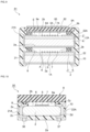
- FIG. 1 A is a front sectional view of an elastic wave device according to a first preferred embodiment of the present invention
- FIG. 1 B is a perspective view for describing the shapes of electrodes on a first main surface side of an element substrate of the elastic wave device of the first preferred embodiment of the present invention.
- FIG. 2 is a perspective view for describing electrode structures provided on a second main surface of the element substrate in the elastic wave device of the first preferred embodiment of the present invention.
- FIG. 3 is a front sectional view of an elastic wave device according to a second preferred embodiment of the present invention.
- FIG. 4 is a plan view illustrating an inductor coil pattern provided on a cover member in the elastic wave device of the second preferred embodiment of the present invention.
- FIG. 5 is a front sectional view of an elastic wave device according to a third preferred embodiment of the present invention.
- FIG. 6 is a front sectional view of an elastic wave device according to a fourth preferred embodiment of the present invention.
- FIG. 7 is a front sectional view of an elastic wave device according to a fifth preferred embodiment of the present invention.
- FIG. 8 is a front sectional view of an elastic wave device according to a sixth preferred embodiment of the present invention.
- FIG. 9 is a front sectional view of an elastic wave device according to a seventh preferred embodiment of the present invention.
- FIG. 10 is a front sectional view of an elastic wave device according to an eighth preferred embodiment of the present invention.
- FIG. 11 is a front sectional view of an elastic wave device according to a modification of the third preferred embodiment of the present invention.
- FIG. 1 A is a front sectional view of an elastic wave device according to a first preferred embodiment of the present invention
- FIG. 1 B is a perspective view for describing electrode structures on a first main surface side of an element substrate used in the first preferred embodiment
- FIG. 2 is a perspective view for describing electrode structures on a second main surface of the element substrate.
- An elastic wave device 1 includes an element substrate 2 .
- the element substrate 2 includes first and second main surfaces 2 a and 2 b , which face each other.
- the element substrate 2 includes a piezoelectric layer 3 and a support substrate 4 .
- the piezoelectric layer 3 is provided on the support substrate 4 . Therefore, the upper surface of the piezoelectric layer 3 defines the second main surface 2 b and the lower surface of the support substrate 4 defines the first main surface 2 a .
- the first main surface 2 a is a mounting-side main surface and the elastic wave device 1 is mounted on a mounting substrate, such as a circuit board, for example, from the first main surface 2 a side.
- the piezoelectric layer 3 is preferably made of a piezoelectric single crystal, such as LiTaO 3 or LiNbO 3 or a piezoelectric ceramic, for example.
- the support substrate 4 is preferably made of a suitable insulator or a semiconductor, for example. Si, Al 2 O 3 , and other suitable materials are examples of a material of the support substrate 4 .
- An IDT electrode 5 and reflectors 6 and 7 which are illustrated in FIG. 1 A , are provided on the second main surface 2 b of the element substrate 2 .
- a plurality of elastic wave resonators 11 to 17 would be provided on the second main surface 2 b in the elastic wave device 1 .
- the elastic wave resonators 11 to 17 are illustrated in a schematic manner using a symbol consisting of an X surrounded by a rectangular frame.
- the elastic wave resonators 11 to 17 are preferably one-port elastic wave resonators, for example.
- the elastic wave resonators 11 to 17 each include the IDT electrode 5 and the reflectors 6 and 7 described above.
- the elastic wave resonators 11 to 17 are electrically connected to each other and define a filter circuit, such as a ladder filter, for example.
- the electrode structures on the second main surface 2 b of the element substrate 2 are not particularly limited and do not need to include reflectors. It is sufficient that at least an IDT electrode that excites an elastic wave is provided.
- the IDT electrode 5 and the reflectors 6 and 7 are preferably made of a suitable metal or alloy such as Al, Cu, or an AlCu alloy, for example.
- the IDT electrode 5 and the reflectors 6 and 7 may include a multilayer metal film in which a plurality of metal films are stacked on top of one another.
- a support layer 8 preferably surrounds the portion in which the IDT electrode 5 and the reflectors 6 and 7 are provided.
- the support layer 8 preferably has a rectangular or substantially rectangular frame shape.
- the support layer 8 is preferably made of a suitable insulating material, such as a composite resin, for example.
- a flat-plate-shaped cover member 9 is mounted on the support layer 8 . As a result, a hollow space A is provided.
- the IDT electrode 5 is located inside the hollow space A.
- a molded resin layer 10 preferably covers side surfaces of a multilayer body including the element substrate 2 , the support layer 8 , and the cover member 9 .
- routing wiring lines 21 and 22 are provided in the elastic wave device 1 . As illustrated in FIG. 1 A , a portion of each of the routing wiring lines 21 and 22 is located on the second main surface 2 b of the element substrate 2 . As illustrated in FIG. 1 A and FIG. 2 , the routing wiring line 21 extends from the second main surface 2 b , across a side surface 2 c , and onto the first main surface 2 a . The routing wiring line 22 extends from the second main surface 2 b , across a side surface 2 d , and onto the first main surface 2 a . As illustrated in FIGS. 1 A and 1 B , the routing wiring line 21 and the routing wiring line 22 are connected to each other on the first main surface 2 a.
- the reason why the routing wiring line 21 and the routing wiring line 22 are preferably connected to each other on the first main surface 2 a is as follows.
- An IDT electrode 5 releases heat when an elastic wave device 1 operates.
- the routing wiring lines are provided on the element substrate 2 to extend up to positions at which the routing wiring lines face a surface of the element substrate 2 on which the IDT electrode 5 is provided, heat dissipating paths along which heat generated by the IDT electrode is transferred to the routing wiring lines via the element substrate 2 become shorter, and therefore, the heat is able to be more efficiently released.
- routing wiring lines 21 and the routing wiring line 22 are connected to each other on the first main surface 2 a , the routing wiring lines are disposed at positions that face the surface of the element substrate 2 on which the IDT electrode 5 is provided, and therefore, this configuration is preferable from the viewpoint of a heat dissipating characteristic.
- routing wiring lines be at a ground potential from the viewpoint of the heat dissipating characteristic.
- routing wiring line 21 and the routing wiring line 22 are not connected to each other on the first main surface 2 a , as long as at least a portion of the routing wiring line 21 and a portion of the routing wiring line 22 are disposed at positions that face the surface of the element substrate 2 on which the IDT electrode 5 is provided, an advantageous effect is achieved from the viewpoint of the heat dissipating characteristic.
- routing wiring lines 21 and 22 In addition to the routing wiring lines 21 and 22 , a plurality of routing wiring lines 23 to 29 are provided.
- the plurality of routing wiring line 21 to 29 extend from the second main surface 2 b , across one of the side surfaces 2 c , 2 d , 2 e , and 2 f , and onto the first main surface 2 a .
- the routing wiring lines 21 to 29 are preferably made of one metal selected from a group consisting of Cu, Au, Pt, and W or an alloy having any one of these metals as a main constituent, for example.
- the routing wiring line 21 is electrically connected to the reflectors and the grounds of the IDT electrodes of elastic wave resonators 13 and 14 illustrated in FIG. 2 .
- the routing wiring line 22 is electrically connected to the reflectors and the ground of the IDT electrode of the elastic wave resonator 15 .
- the routing wiring lines 21 and 22 are not particularly restricted and preferably have a band shape, for example.
- the other routing wiring lines 23 to 29 also similarly have a band shape, for example. There is a high degree of freedom regarding the dimensions of the band shape, such as the width. Therefore, there is a high degree of freedom in terms of design.
- the routing wiring lines 21 and 22 extend from inside the hollow space A to outside the hollow space A on the second main surface 2 b , extend across the side surface 2 c or 2 d , and onto the first main surface 2 a .
- a heat dissipating characteristic is effectively improved.
- the elastic wave device 1 When the elastic wave device 1 is driven, heat is primarily generated in the IDT electrode 5 . Since the element substrate 2 does not have a particularly high thermal conductivity, it is difficult for the heat to dissipate. However, in the elastic wave device 1 , taking the routing wiring lines 21 and 22 as examples, the routing wiring lines 21 and 22 are electrically connected to the IDT electrode, and therefore, the heat rapidly moves toward the first main surface 2 a side via the band-shaped routing wiring lines 21 and 22 . In addition, the heat generated in the IDT electrode 5 is also transferred to the piezoelectric layer 3 and the support substrate 4 . Therefore, heat moves as indicated by arrows B 1 to B 6 in FIGS. 1 A and 1 B .
- the routing wiring lines 21 to 29 it is sufficient for the routing wiring lines 21 to 29 to extend from a surface of the element substrate 2 onto side surfaces of the element substrate 2 .
- the routing wiring lines 21 to 29 may extend onto the first main surface 2 a , which is the lower surface. Therefore, there is no need to perform troublesome through hole processing. Consequently, the elastic wave device 1 is easy to manufacture.
- the IDT electrode 5 is provided on the second main surface 2 b rather than the mounting-surface-side first main surface 2 a . Therefore, the lengths of the routing wiring lines 21 to 29 are relatively short. Consequently, the heat dissipating characteristic is sufficiently high.
- the routing wiring line 21 is connected to the ground potential.
- the routing wiring line 23 is connected to a signal potential. Therefore, the routing wiring line 21 and the routing wiring line 23 are connected to different potentials.
- the routing wiring line 21 and the routing wiring line 23 are arranged with a gap G therebetween on the side surface 2 c . Therefore, short circuits between the routing wiring lines 21 and 23 are effectively reduced or prevented.
- routing wiring lines that are connected to different potentials may be separated by a gap G on the same side surface 2 c in this manner, for example.
- routing wiring lines that are connected to different potentials may be arranged on different side surfaces as in the case of the routing wiring line 23 and the routing wiring line 26 .
- routing wiring lines that are connected to different potentials may be separated by gaps on a plurality of side surfaces.
- the meaning of “on a plurality of side surfaces” also includes a configuration in which routing wiring lines that are arranged on not just one side surface but on two adjacent side surfaces, for example, are separated by a gap.
- the routing wiring lines 21 to 29 preferably cover portions of the side surfaces 2 c to 2 f .
- the routing wiring lines may cover the entirety or substantially the entirety of at least one of the side surfaces 2 c , 2 d , 2 e , and 2 f .
- the routing wiring line 26 illustrated in FIG. 1 B may cover the entire side surface 2 f . In this manner, the heat dissipating characteristics are further improved. In this case, it is sufficient that the routing wiring lines 23 and 24 extend across the side surface 2 c or the side surface 2 d onto the first main surface 2 a.
- a direction indicated by arrow C in FIG. 2 is an elastic wave propagation direction and the electrode fingers of the IDT electrode 5 extend in a direction that is perpendicular or substantially perpendicular to the direction indicated by arrow C.
- the routing wiring line 21 is provided at a position at which the routing wiring line 21 is superposed with the IDT electrode 5 of the elastic wave resonator 14 in the elastic wave propagation direction of the elastic wave resonator 14 .
- the routing wiring line 21 is preferably larger than the largest outer dimension of the IDT electrode of the elastic wave resonator 14 .
- the largest outer dimension of the IDT electrode refers to the largest dimension of the IDT electrode among a dimension of the IDT electrode in the elastic wave propagation direction and a dimension of the IDT electrode in a direction that is perpendicular or substantially perpendicular to the elastic wave propagation direction. It is further preferable that a dimension W of the routing wiring line 21 in a width direction be larger than an outer dimension of the IDT electrode 5 in the direction in which the electrode fingers of the IDT electrode 5 of the elastic wave resonator 14 extend.
- “Dimension W in the width direction” refers to a dimension in a direction that is perpendicular or substantially perpendicular to a direction in which the routing wiring line 21 is routed. “Direction in which the routing wiring line is routed” refers to a routing direction in which the routing wiring line extends from the second main surface 2 b , across the side surface 2 c , and onto the first main surface 2 a , as described above.
- the width direction dimension W of the routing wiring line 21 is preferably larger than an outer dimension of the IDT electrode in the direction in which the electrode fingers of the IDT electrode extend. Therefore, heat generated at the peripheral edges of the IDT electrode 5 is able to be absorbed and the heat dissipating characteristic is further improved.
- the heat dissipating characteristic is effectively improved.
- the routing wiring line 21 and the routing wiring line 22 do not need to be connected to each other on the first main surface 2 a .
- the plurality of routing wiring lines 21 to 29 extend onto the first main surface 2 a
- the plurality of routing wiring lines 21 to 29 do not need to extend onto the first main surface 2 a . Even in such a case, heat transferred to the side surfaces 2 c to 2 f rapidly moves to the routing wiring lines 21 to 29 .
- the plurality of routing wiring lines 21 to 29 are preferably provided to extend onto the first main surface 2 a . In this manner, the heat dissipating characteristic is further improved.
- routing wiring line 21 is electrically connected to the IDT electrode and the reflectors, it is sufficient that each of the routing wiring lines 21 to 29 be electrically connected to at least one of the reflectors and the IDT electrode. It is preferable that at least one routing wiring line among the routing wiring lines 21 to 29 be electrically connected to the corresponding IDT electrode.
- the IDT electrode is a heat-generating element, and therefore, the heat dissipating characteristic is able to be more effectively improved.
- the element substrate 2 has a structure in which the piezoelectric layer 3 is stacked on the support substrate 4 .
- the support substrate 4 be made of a material having a higher thermal conductivity than the piezoelectric layer 3 .
- Si or other suitable material is an example of such a material.
- the thermal conductivity of the support substrate 4 is higher than the thermal conductivity of the piezoelectric layer 3 , the heat dissipating characteristic is further improved.
- FIG. 3 is a front sectional view of an elastic wave device 31 according to a second preferred embodiment of the present invention.
- the elastic wave device 31 is the same or substantially the same as the elastic wave device 1 of the first preferred embodiment except that the elastic wave device 31 includes capacitor electrodes 32 and 33 and an inductor coil pattern 34 and in that the routing wiring lines 21 and 22 are not connected to each other on the first main surface 2 a.
- the capacitor electrode 32 is provided on a lower surface 9 a of the cover member 9 .
- the capacitor electrode 33 is provided on an upper surface 9 b of the cover member 9 .
- the capacitor electrode 32 and the capacitor electrode 33 are preferably superposed with each other with the cover member 9 interposed therebetween. As a result, a capacitor is provided.
- the inductor coil pattern 34 illustrated in FIG. 4 is provided on the lower surface 9 a of the cover member 9 .
- the inductor coil pattern 34 is preferably made of a metal or an alloy such as Cu, for example.
- the inductor coil pattern 34 defines an inductor.
- the inductor coil pattern 34 is electrically connected to the capacitor electrode 33 by a via hole electrode 35 .
- an LC circuit is provided on the cover member 9 .
- This LC circuit is electrically connected to a functional electrode portion of the elastic wave device 31 including the IDT electrode 5 .
- a capacitor and an inductor may be provided on the cover member 9 .
- only one of the capacitor and the inductor may be provided on the cover member 9 instead.
- an outer electrode 36 is provided on the routing wiring line 21 on the first main surface 2 a .
- An outer electrode 37 is provided on the routing wiring line 22 .
- a plurality of routing wiring lines including the routing wiring lines 21 and 22 extend from the second main surface 2 b of the element substrate 2 , across the side surface 2 c , 2 d , and so on, and onto the first main surface 2 a . Therefore, similarly to the case of the elastic wave device of the first preferred embodiment, the heat dissipating characteristic is improved. In addition, the manufacturing process is easy.
- FIG. 5 is a front sectional view illustrating an elastic wave device 41 according to a third preferred embodiment of the present invention.
- the elastic wave device 41 includes an element substrate 2 preferably including only a piezoelectric layer.
- the element substrate 2 is preferably made of the same material as the piezoelectric layer 3 described above. Thus, in the present preferred embodiment, the element substrate 2 may include only a piezoelectric layer.
- an insulating layer 42 preferably extends from the second main surface 2 b of the element substrate 2 , across the side surfaces 2 c and 2 d , and onto the first main surface 2 a .
- the routing wiring lines 21 and 22 are preferably stacked on the insulating layer 42 .
- the insulating layer 42 is preferably made of a resin or an inorganic insulating material, for example.
- a suitable composite resin, such as an epoxy resin or a silicone resin, is an example of such a resin. Silicon oxide, silicon nitride, silicon oxynitride, alumina, tantalum oxide, and other suitable materials are examples of such an inorganic insulating material.
- the insulating layer 42 is provided as an underlayer for the routing wiring lines 21 and 22 .
- the insulating layer 42 is provided between the routing wiring lines 21 and 22 and the element substrate 2 . Then, in the case in which the insulating layer 42 is made of a resin, breakages are unlikely to occur in the routing wiring lines 21 and 22 . This is because in the case in which the elastic wave device 41 is mounted on a mounting substrate or in the case in which heat acts on the elastic wave device 41 , the element substrate 2 expands and contracts and, therefore, stress acts on the routing wiring lines 21 and 22 .
- the insulating layer 42 which is made of resin, is provided as an underlayer between the routing wiring lines 21 and 22 and the element substrate 2 , stress acting on the routing wiring lines 21 and 22 is effectively reduced.
- the locations at which the greatest stress acts on the routing wiring lines 21 and 22 are, for example, the corner portions in the cross section in FIG. 5 as indicated by arrows E 1 , E 2 , E 3 , and E 4 , it is preferable that the insulating layer 42 made of a resin is provided as an underlayer for the routing wiring lines 21 and 22 at the corner portions in the cross section in FIG. 5 as indicated by the arrows E 1 , E 2 , E 3 , and E 4 . Therefore, it is preferable that the insulating layer 42 made of a resin is provided as an underlayer for the routing wiring lines 21 and 22 at the edges between the second main surface 2 b or the first main surface 2 a and the side surfaces 2 c to 2 f.
- the elastic wave device 41 is the same or substantially the same as the elastic wave device 31 in all other respects. Therefore, the same elements are denoted by the same reference symbols and description thereof is omitted. Since a plurality of routing wiring lines including the routing wiring lines 21 and 22 are provided in the elastic wave device 41 , the heat dissipating paths are increased and, therefore, the heat dissipating characteristic is effectively improved. In addition, there is no need to provide through holes and, therefore, the manufacturing process is also easy.
- FIG. 11 is a front sectional view illustrating a modification of the third preferred embodiment of the present invention.
- the modification of the third preferred embodiment differs from the third preferred embodiment in that the element substrate 2 includes the support substrate 4 .
- the modification is the same or substantially the same as the third preferred embodiment in all other respects.
- the support substrate 4 of the elastic wave device 41 includes a substrate having conductivity, such as a silicon substrate, a leakage current is undesirably generated between the routing wiring line 21 and the routing wiring line 22 via the support substrate 4 and the characteristics of the elastic wave device 41 are undesirably degraded.
- an insulating layer 42 made of an inorganic insulating material as an underlayer between the routing wiring lines 21 and 22 and the support substrate 4 .
- silicon oxide, silicon nitride, silicon oxynitride, alumina, tantalum oxide, and other suitable materials are examples of such an inorganic insulating material.
- FIG. 6 is a front sectional view of an elastic wave device 51 according to a fourth preferred embodiment of the present invention.
- the elastic wave device 51 includes an elastic wave device 1 A, which is obtained by removing the cover member 9 from the elastic wave device 1 illustrated in FIGS. 1 A and 1 B .
- An elastic wave device 52 is arranged on the elastic wave device 1 A.
- the elastic wave device 52 corresponds to a cover member of the elastic wave device 1 A.
- a plurality of elastic wave devices may be stacked on top of one another as in the present preferred embodiment.
- the elastic wave device 52 preferably has the same or substantially the same structure as the elastic wave device 1 A.
- the elastic wave device 52 is vertically inverted with respect to the elastic wave device 1 A. Therefore, the second main surfaces 2 b face each other in the hollow space A.
- an IDT electrode 5 A and reflectors 6 A and 7 A are provided on another element substrate 2 A, which is different from the element substrate 2 .
- the elastic wave device 52 includes routing wiring lines 21 A and 22 A.
- the routing wiring lines 21 A and 22 A extend from the second main surface 2 b onto the side surfaces 2 c and 2 d , but do not extend onto the first main surface 2 a .
- the remaining configuration of the elastic wave device 52 is the same or substantially the same as that of the elastic wave device 1 A.
- the plurality of routing wiring lines of the elastic wave device 52 including the routing wiring lines 21 A and 22 A are electrically connected, as appropriate, to the plurality of routing wiring lines 21 , 22 of the elastic wave device 1 A. Consequently, the elastic wave device 1 A and the elastic wave device 52 are electrically connected to each other and a filter circuit or other suitable circuit is thus provided.
- the elastic wave device 1 A has the same or substantially the same configuration as the elastic wave device 1 , the elastic wave device 51 has an excellent heat dissipating characteristic and is easy to manufacture. Furthermore, the elastic wave device 52 , which is stacked to define a cover member, also includes a plurality of routing wiring lines including the routing wiring lines 21 A and 22 A, and therefore, the elastic wave device 52 similarly has an excellent heat dissipating characteristic. In addition, since there is no need to perform through hole processing, the manufacturing process is easy.
- the element substrates 2 and 2 A are each preferably defined by a multilayer body including the support substrate 4 and the piezoelectric layer 3 .
- the element substrates 2 and 2 A may, instead, be defined by only a piezoelectric layer.
- FIG. 7 is a front sectional view of an elastic wave device 61 according to a fifth preferred embodiment of the present invention.
- the routing wiring lines 21 A and 22 A are connected to each other on the first main surface 2 a .
- the remaining configuration of the elastic wave device 61 is the same or substantially the same as that of the elastic wave device 51 .
- a plurality of routing wiring lines 21 A and 22 A may be connected to each other on the first main surface 2 a , and in this case, the heat dissipating characteristic is further improved.
- FIG. 8 is a front sectional view of an elastic wave device 71 according to a sixth preferred embodiment of the present invention.
- an elastic wave device 52 B is stacked above the elastic wave device 1 A, instead of a cover member.
- the first main surface 2 a in the elastic wave device 52 B faces the second main surface 2 b in the elastic wave device 1 A.
- the vertical orientation of the elastic wave device 52 B is the same as the vertical orientation of the elastic wave device 1 A. Consequently, a support layer 8 A and a cover member 9 A are provided on the second main surface 2 b in the elastic wave device 52 B.
- a hollow space E is provided.
- the elastic wave device 52 B includes a plurality of routing wiring lines 21 A and 22 A, similarly to the elastic wave devices 51 and 61 , the elastic wave device 71 is able to effectively improve the heat dissipating characteristic in both of the elastic wave device 1 A and the elastic wave device 52 B. In addition, there is no need to provide through holes and, therefore, the manufacturing process is also easy.
- FIG. 9 is a front sectional view of an elastic wave device 81 according to a seventh preferred embodiment of the present invention.
- capacitor electrodes 82 and 83 are provided on the lower surface 9 a and the upper surface 9 b of the cover member 9 A.
- a capacitor is defined by the capacitor electrodes 82 and 83 .
- the remaining configuration of the elastic wave device 81 is the same or substantially the same as that of the elastic wave device 71 . Therefore, the heat dissipating characteristic is improved in the elastic wave device 81 . In addition, the manufacturing process is also easy.
- FIG. 10 is a front sectional view of an elastic wave device 91 according to an eighth preferred embodiment of the present invention.
- the elastic wave device 91 according the eighth preferred embodiment includes an element substrate 2 defined by a piezoelectric body.
- a level difference is provided on the second main surface 2 b side of the element substrate 2 .
- a direction that connects the side surface 2 c and the side surface 2 d that faces the side surface 2 c to each other is denoted as a width direction.
- the width direction dimension that is, the width is smaller on the second main surface 2 b side than on the first main surface 2 a side.
- level differences 2 x and 2 y are provided on the outer sides in the width direction. Thus, portions having a relatively smaller width are provided on the second main surface 2 b side.
- the element substrate 2 defined by a piezoelectric body an element substrate in which a piezoelectric layer is provided on a support substrate may be used, instead, as in the first preferred embodiment described above.
- the level differences 2 x and 2 y may be provided in the piezoelectric layer and may extend to the support substrate below the piezoelectric layer.
- the other portions and elements of the elastic wave device 91 are the same or substantially the same as those of the elastic wave device 1 of the first preferred embodiment, and therefore, the same portions and elements are denoted by the same reference symbols and reference should be made to the description given in the first preferred embodiment.
- the cover member 9 covers the upper surface of the molded resin layer 10 in the present preferred embodiment, the present invention is not limited to this configuration.
- the molded resin layer 10 may extend onto side surfaces of the cover member 9 .
- the method of providing the element substrate 2 with portions having a relatively small width is not particularly limited.
- cutting is performed using the dicing machine a first time in order to divide the collective board into individual element substrates.
- shallow cutting is performed using the dicing machine using a blade having a larger width than the blade used when performing the cutting the first time.
- the level differences 2 x and 2 y are provided.
Landscapes
- Physics & Mathematics (AREA)
- Acoustics & Sound (AREA)
- Surface Acoustic Wave Elements And Circuit Networks Thereof (AREA)
Applications Claiming Priority (3)
| Application Number | Priority Date | Filing Date | Title |
|---|---|---|---|
| JP2015-248813 | 2015-12-21 | ||
| JP2015248813 | 2015-12-21 | ||
| PCT/JP2016/083779 WO2017110308A1 (ja) | 2015-12-21 | 2016-11-15 | 弾性波装置 |
Related Parent Applications (1)
| Application Number | Title | Priority Date | Filing Date |
|---|---|---|---|
| PCT/JP2016/083779 Continuation WO2017110308A1 (ja) | 2015-12-21 | 2016-11-15 | 弾性波装置 |
Publications (2)
| Publication Number | Publication Date |
|---|---|
| US20180269849A1 US20180269849A1 (en) | 2018-09-20 |
| US11695388B2 true US11695388B2 (en) | 2023-07-04 |
Family
ID=59089318
Family Applications (1)
| Application Number | Title | Priority Date | Filing Date |
|---|---|---|---|
| US15/983,322 Active 2040-09-11 US11695388B2 (en) | 2015-12-21 | 2018-05-18 | Elastic wave device |
Country Status (2)
| Country | Link |
|---|---|
| US (1) | US11695388B2 (ja) |
| WO (1) | WO2017110308A1 (ja) |
Cited By (1)
| Publication number | Priority date | Publication date | Assignee | Title |
|---|---|---|---|---|
| US12331734B2 (en) * | 2020-09-30 | 2025-06-17 | Murata Manufacturing Co., Ltd. | Fluid control device |
Families Citing this family (12)
| Publication number | Priority date | Publication date | Assignee | Title |
|---|---|---|---|---|
| WO2016208287A1 (ja) * | 2015-06-24 | 2016-12-29 | 株式会社村田製作所 | 弾性波フィルタ装置 |
| JP6449836B2 (ja) * | 2016-11-25 | 2019-01-09 | 太陽誘電株式会社 | 電子部品およびその製造方法 |
| WO2018105201A1 (ja) * | 2016-12-08 | 2018-06-14 | 株式会社村田製作所 | 複合部品及びその実装構造 |
| JP2019114985A (ja) | 2017-12-25 | 2019-07-11 | 株式会社村田製作所 | 複合電子部品 |
| WO2020179458A1 (ja) | 2019-03-07 | 2020-09-10 | 株式会社村田製作所 | 電子部品 |
| WO2021079905A1 (ja) | 2019-10-24 | 2021-04-29 | 株式会社村田製作所 | 弾性波装置 |
| WO2021079910A1 (ja) * | 2019-10-24 | 2021-04-29 | 株式会社村田製作所 | 弾性波装置 |
| US12016247B2 (en) * | 2020-08-27 | 2024-06-18 | Qualcomm Incorporated | Package comprising an integrated passive device configured as a cap for a filter |
| US12261583B2 (en) * | 2022-02-04 | 2025-03-25 | Rf360 Singapore Pte. Ltd. | Stacked acoustic wave (AW) filter packages, including cross-talk reduction layers, and related fabrication methods |
| US12401345B2 (en) * | 2022-09-01 | 2025-08-26 | Rf360 Singapore Pte. Ltd. | Stacked acoustic wave (AW) packages with reduced excitation of reflected bulk waves |
| CN115694409A (zh) * | 2022-11-10 | 2023-02-03 | 武汉敏声新技术有限公司 | 一种谐振器封装结构及方法 |
| US20240333260A1 (en) * | 2023-03-28 | 2024-10-03 | Skyworks Solutions, Inc. | Stacked surface acoustic wave device |
Citations (18)
| Publication number | Priority date | Publication date | Assignee | Title |
|---|---|---|---|---|
| US5237235A (en) * | 1991-09-30 | 1993-08-17 | Motorola, Inc. | Surface acoustic wave device package |
| US5281883A (en) * | 1990-11-05 | 1994-01-25 | Fujitsu Limited | Surface acoustic wave device with improved junction bonding and package miniaturization |
| JP2000165192A (ja) | 1998-11-30 | 2000-06-16 | Kyocera Corp | 弾性表面波装置 |
| US20020149295A1 (en) | 1999-06-14 | 2002-10-17 | Matsushita Electric Industrial Co., Ltd. | Surface acoustic wave element, method for producing the same and surface acoustic wave device using the same |
| JP2003087073A (ja) | 2001-09-14 | 2003-03-20 | Murata Mfg Co Ltd | 端面反射型表面波装置及びその製造方法 |
| US6801100B2 (en) * | 1996-05-23 | 2004-10-05 | Matsushita Electric Industrial Co., Ltd. | Inter-digital transducer, surface acoustic wave filter and communication apparatus using the same |
| US20040196119A1 (en) * | 2003-02-24 | 2004-10-07 | Teruhisa Shibahara | Surface acoustic wave filter and communication apparatus |
| US7391090B2 (en) * | 2004-12-17 | 2008-06-24 | Hewlett-Packard Development Company, L.P. | Systems and methods for electrically coupling wires and conductors |
| JP2008546207A (ja) | 2005-06-07 | 2008-12-18 | エプコス アクチエンゲゼルシャフト | 電気的素子および製造方法 |
| JP2009159195A (ja) | 2007-12-26 | 2009-07-16 | Nippon Dempa Kogyo Co Ltd | 圧電部品及びその製造方法 |
| US7808935B2 (en) * | 2006-03-08 | 2010-10-05 | Kyocera Corporation | Duplexer and communication device |
| WO2014034326A1 (ja) | 2012-08-29 | 2014-03-06 | 株式会社村田製作所 | 弾性波装置 |
| US8674498B2 (en) * | 2007-12-07 | 2014-03-18 | Epcos Ag | MEMS package and method for the production thereof |
| US20140252916A1 (en) | 2013-03-08 | 2014-09-11 | Triquint Semiconductor, Inc. | Acoustic wave device |
| US8963655B2 (en) * | 2009-11-27 | 2015-02-24 | Kyocera Corporation | Acoustic wave device and method for producing same |
| WO2015098792A1 (ja) | 2013-12-25 | 2015-07-02 | 株式会社村田製作所 | 弾性波フィルタデバイス |
| US9831850B2 (en) * | 2015-02-19 | 2017-11-28 | Taiyo Yuden Co., Ltd. | Acoustic wave device with a piezoelectric substrate that is not located in some regions |
| US20180013055A1 (en) * | 2015-02-27 | 2018-01-11 | Epcos Ag | Mems component having a high integration density |
-
2016
- 2016-11-15 WO PCT/JP2016/083779 patent/WO2017110308A1/ja not_active Ceased
-
2018
- 2018-05-18 US US15/983,322 patent/US11695388B2/en active Active
Patent Citations (26)
| Publication number | Priority date | Publication date | Assignee | Title |
|---|---|---|---|---|
| US5281883A (en) * | 1990-11-05 | 1994-01-25 | Fujitsu Limited | Surface acoustic wave device with improved junction bonding and package miniaturization |
| US5237235A (en) * | 1991-09-30 | 1993-08-17 | Motorola, Inc. | Surface acoustic wave device package |
| US6801100B2 (en) * | 1996-05-23 | 2004-10-05 | Matsushita Electric Industrial Co., Ltd. | Inter-digital transducer, surface acoustic wave filter and communication apparatus using the same |
| JP2000165192A (ja) | 1998-11-30 | 2000-06-16 | Kyocera Corp | 弾性表面波装置 |
| US20020149295A1 (en) | 1999-06-14 | 2002-10-17 | Matsushita Electric Industrial Co., Ltd. | Surface acoustic wave element, method for producing the same and surface acoustic wave device using the same |
| JP2009118504A (ja) | 1999-06-14 | 2009-05-28 | Panasonic Corp | 弾性表面波素子 |
| US20030071539A1 (en) | 2001-09-14 | 2003-04-17 | Yasuhiro Kuratani | Edge reflection type surface acoustic wave device and manufacturing method for the same |
| JP2003087073A (ja) | 2001-09-14 | 2003-03-20 | Murata Mfg Co Ltd | 端面反射型表面波装置及びその製造方法 |
| US20040196119A1 (en) * | 2003-02-24 | 2004-10-07 | Teruhisa Shibahara | Surface acoustic wave filter and communication apparatus |
| US7295089B2 (en) * | 2003-02-24 | 2007-11-13 | Murata Manufacturing Co., Ltd. | Surface acoustic wave filter and communication apparatus |
| US7391090B2 (en) * | 2004-12-17 | 2008-06-24 | Hewlett-Packard Development Company, L.P. | Systems and methods for electrically coupling wires and conductors |
| JP2008546207A (ja) | 2005-06-07 | 2008-12-18 | エプコス アクチエンゲゼルシャフト | 電気的素子および製造方法 |
| US20090224851A1 (en) | 2005-06-07 | 2009-09-10 | Epcos Ag | Electrical component and production method |
| US7808935B2 (en) * | 2006-03-08 | 2010-10-05 | Kyocera Corporation | Duplexer and communication device |
| US8674498B2 (en) * | 2007-12-07 | 2014-03-18 | Epcos Ag | MEMS package and method for the production thereof |
| JP2009159195A (ja) | 2007-12-26 | 2009-07-16 | Nippon Dempa Kogyo Co Ltd | 圧電部品及びその製造方法 |
| US8963655B2 (en) * | 2009-11-27 | 2015-02-24 | Kyocera Corporation | Acoustic wave device and method for producing same |
| WO2014034326A1 (ja) | 2012-08-29 | 2014-03-06 | 株式会社村田製作所 | 弾性波装置 |
| US20150109071A1 (en) | 2012-08-29 | 2015-04-23 | Murata Manufacturing Co., Ltd. | Elastic wave device |
| US20140252916A1 (en) | 2013-03-08 | 2014-09-11 | Triquint Semiconductor, Inc. | Acoustic wave device |
| JP2014176089A (ja) | 2013-03-08 | 2014-09-22 | Triquint Semiconductor Inc | 弾性波デバイスおよびそれを形成する方法 |
| WO2015098792A1 (ja) | 2013-12-25 | 2015-07-02 | 株式会社村田製作所 | 弾性波フィルタデバイス |
| US20160301386A1 (en) | 2013-12-25 | 2016-10-13 | Murata Manufacturing Co., Ltd. | Elastic wave filter device |
| US9831850B2 (en) * | 2015-02-19 | 2017-11-28 | Taiyo Yuden Co., Ltd. | Acoustic wave device with a piezoelectric substrate that is not located in some regions |
| US20180013055A1 (en) * | 2015-02-27 | 2018-01-11 | Epcos Ag | Mems component having a high integration density |
| US10680159B2 (en) * | 2015-02-27 | 2020-06-09 | Snaptrack, Inc. | MEMS component having a high integration density |
Non-Patent Citations (1)
| Title |
|---|
| Official Communication issued in International Patent Application No. PCT/JP2016/083779, dated Feb. 7, 2017. |
Cited By (1)
| Publication number | Priority date | Publication date | Assignee | Title |
|---|---|---|---|---|
| US12331734B2 (en) * | 2020-09-30 | 2025-06-17 | Murata Manufacturing Co., Ltd. | Fluid control device |
Also Published As
| Publication number | Publication date |
|---|---|
| WO2017110308A1 (ja) | 2017-06-29 |
| US20180269849A1 (en) | 2018-09-20 |
Similar Documents
| Publication | Publication Date | Title |
|---|---|---|
| US11695388B2 (en) | Elastic wave device | |
| CN109417054B (zh) | 高频用陶瓷基板及高频用半导体元件收纳封装体 | |
| US10917069B2 (en) | Electronic component | |
| US10320362B2 (en) | Elastic wave device | |
| US10622964B2 (en) | Elastic wave device | |
| US11165390B2 (en) | Piezoelectric resonator device | |
| JPWO2006001125A1 (ja) | 圧電デバイス | |
| US9654081B2 (en) | Electronic component and manufacturing method therefor | |
| US11509289B2 (en) | Composite component and mounting structure therefor | |
| CN105814796A (zh) | 弹性波滤波器设备 | |
| US11764753B2 (en) | Elastic wave device and electronic component | |
| CN110771037B (zh) | 弹性波装置、前端电路以及通信装置 | |
| US10411672B2 (en) | Elastic wave device | |
| KR20170121702A (ko) | 회로 모듈 | |
| KR102163886B1 (ko) | 탄성파 장치 | |
| JPWO2018235876A1 (ja) | 弾性波装置、フロントエンド回路及び通信装置 | |
| US9065420B2 (en) | Fabrication method of acoustic wave device | |
| KR101987712B1 (ko) | 탄성파 장치의 제조 방법 및 탄성파 장치 | |
| US9935610B2 (en) | Acoustic wave device | |
| JP2022165445A (ja) | 半導体装置 | |
| US10581401B2 (en) | Module device | |
| US10812041B2 (en) | Elastic wave device and manufacturing method for same | |
| JP5467375B2 (ja) | 弾性表面波デバイス | |
| WO2024143086A1 (ja) | 弾性波デバイス、その製造方法およびモジュール | |
| JP6370652B2 (ja) | 半導体装置 |
Legal Events
| Date | Code | Title | Description |
|---|---|---|---|
| AS | Assignment |
Owner name: MURATA MANUFACTURING CO., LTD., JAPAN Free format text: ASSIGNMENT OF ASSIGNORS INTEREST;ASSIGNORS:MATSUMOTO, KATSUYA;NOMIYA, MASATO;SIGNING DATES FROM 20180508 TO 20180510;REEL/FRAME:045842/0655 |
|
| FEPP | Fee payment procedure |
Free format text: ENTITY STATUS SET TO UNDISCOUNTED (ORIGINAL EVENT CODE: BIG.); ENTITY STATUS OF PATENT OWNER: LARGE ENTITY |
|
| STPP | Information on status: patent application and granting procedure in general |
Free format text: DOCKETED NEW CASE - READY FOR EXAMINATION |
|
| STPP | Information on status: patent application and granting procedure in general |
Free format text: NON FINAL ACTION MAILED |
|
| STPP | Information on status: patent application and granting procedure in general |
Free format text: RESPONSE TO NON-FINAL OFFICE ACTION ENTERED AND FORWARDED TO EXAMINER |
|
| STPP | Information on status: patent application and granting procedure in general |
Free format text: FINAL REJECTION MAILED |
|
| STCF | Information on status: patent grant |
Free format text: PATENTED CASE |