US11682720B2 - Switching transistor and semiconductor module to suppress signal distortion - Google Patents
Switching transistor and semiconductor module to suppress signal distortion Download PDFInfo
- Publication number
- US11682720B2 US11682720B2 US17/047,453 US201917047453A US11682720B2 US 11682720 B2 US11682720 B2 US 11682720B2 US 201917047453 A US201917047453 A US 201917047453A US 11682720 B2 US11682720 B2 US 11682720B2
- Authority
- US
- United States
- Prior art keywords
- layer
- barrier layer
- switching transistor
- channel
- insulating film
- Prior art date
- Legal status (The legal status is an assumption and is not a legal conclusion. Google has not performed a legal analysis and makes no representation as to the accuracy of the status listed.)
- Active, expires
Links
Images


Classifications
-
- H01L29/778—
-
- H—ELECTRICITY
- H10—SEMICONDUCTOR DEVICES; ELECTRIC SOLID-STATE DEVICES NOT OTHERWISE PROVIDED FOR
- H10D—INORGANIC ELECTRIC SEMICONDUCTOR DEVICES
- H10D30/00—Field-effect transistors [FET]
- H10D30/40—FETs having zero-dimensional [0D], one-dimensional [1D] or two-dimensional [2D] charge carrier gas channels
- H10D30/47—FETs having zero-dimensional [0D], one-dimensional [1D] or two-dimensional [2D] charge carrier gas channels having 2D charge carrier gas channels, e.g. nanoribbon FETs or high electron mobility transistors [HEMT]
-
- H—ELECTRICITY
- H10—SEMICONDUCTOR DEVICES; ELECTRIC SOLID-STATE DEVICES NOT OTHERWISE PROVIDED FOR
- H10D—INORGANIC ELECTRIC SEMICONDUCTOR DEVICES
- H10D62/00—Semiconductor bodies, or regions thereof, of devices having potential barriers
- H10D62/80—Semiconductor bodies, or regions thereof, of devices having potential barriers characterised by the materials
- H10D62/85—Semiconductor bodies, or regions thereof, of devices having potential barriers characterised by the materials being Group III-V materials, e.g. GaAs
-
- H—ELECTRICITY
- H01—ELECTRIC ELEMENTS
- H01L—SEMICONDUCTOR DEVICES NOT COVERED BY CLASS H10
- H01L21/00—Processes or apparatus adapted for the manufacture or treatment of semiconductor or solid state devices or of parts thereof
- H01L21/02—Manufacture or treatment of semiconductor devices or of parts thereof
- H01L21/02104—Forming layers
- H01L21/02365—Forming inorganic semiconducting materials on a substrate
- H01L21/02518—Deposited layers
- H01L21/0257—Doping during depositing
- H01L21/02573—Conductivity type
-
- H—ELECTRICITY
- H01—ELECTRIC ELEMENTS
- H01L—SEMICONDUCTOR DEVICES NOT COVERED BY CLASS H10
- H01L21/00—Processes or apparatus adapted for the manufacture or treatment of semiconductor or solid state devices or of parts thereof
- H01L21/02—Manufacture or treatment of semiconductor devices or of parts thereof
- H01L21/04—Manufacture or treatment of semiconductor devices or of parts thereof the devices having potential barriers, e.g. a PN junction, depletion layer or carrier concentration layer
- H01L21/18—Manufacture or treatment of semiconductor devices or of parts thereof the devices having potential barriers, e.g. a PN junction, depletion layer or carrier concentration layer the devices having semiconductor bodies comprising elements of Group IV of the Periodic Table or AIIIBV compounds with or without impurities, e.g. doping materials
- H01L21/28—Manufacture of electrodes on semiconductor bodies using processes or apparatus not provided for in groups H01L21/20 - H01L21/268
-
- H01L29/45—
-
- H01L29/49—
-
- H01L29/6653—
-
- H01L29/786—
-
- H—ELECTRICITY
- H10—SEMICONDUCTOR DEVICES; ELECTRIC SOLID-STATE DEVICES NOT OTHERWISE PROVIDED FOR
- H10D—INORGANIC ELECTRIC SEMICONDUCTOR DEVICES
- H10D30/00—Field-effect transistors [FET]
- H10D30/01—Manufacture or treatment
- H10D30/015—Manufacture or treatment of FETs having heterojunction interface channels or heterojunction gate electrodes, e.g. HEMT
-
- H—ELECTRICITY
- H10—SEMICONDUCTOR DEVICES; ELECTRIC SOLID-STATE DEVICES NOT OTHERWISE PROVIDED FOR
- H10D—INORGANIC ELECTRIC SEMICONDUCTOR DEVICES
- H10D30/00—Field-effect transistors [FET]
- H10D30/40—FETs having zero-dimensional [0D], one-dimensional [1D] or two-dimensional [2D] charge carrier gas channels
- H10D30/47—FETs having zero-dimensional [0D], one-dimensional [1D] or two-dimensional [2D] charge carrier gas channels having 2D charge carrier gas channels, e.g. nanoribbon FETs or high electron mobility transistors [HEMT]
- H10D30/471—High electron mobility transistors [HEMT] or high hole mobility transistors [HHMT]
- H10D30/473—High electron mobility transistors [HEMT] or high hole mobility transistors [HHMT] having confinement of carriers by multiple heterojunctions, e.g. quantum well HEMT
- H10D30/4732—High electron mobility transistors [HEMT] or high hole mobility transistors [HHMT] having confinement of carriers by multiple heterojunctions, e.g. quantum well HEMT using Group III-V semiconductor material
-
- H—ELECTRICITY
- H10—SEMICONDUCTOR DEVICES; ELECTRIC SOLID-STATE DEVICES NOT OTHERWISE PROVIDED FOR
- H10D—INORGANIC ELECTRIC SEMICONDUCTOR DEVICES
- H10D30/00—Field-effect transistors [FET]
- H10D30/40—FETs having zero-dimensional [0D], one-dimensional [1D] or two-dimensional [2D] charge carrier gas channels
- H10D30/47—FETs having zero-dimensional [0D], one-dimensional [1D] or two-dimensional [2D] charge carrier gas channels having 2D charge carrier gas channels, e.g. nanoribbon FETs or high electron mobility transistors [HEMT]
- H10D30/471—High electron mobility transistors [HEMT] or high hole mobility transistors [HHMT]
- H10D30/475—High electron mobility transistors [HEMT] or high hole mobility transistors [HHMT] having wider bandgap layer formed on top of lower bandgap active layer, e.g. undoped barrier HEMTs such as i-AlGaN/GaN HEMTs
-
- H—ELECTRICITY
- H10—SEMICONDUCTOR DEVICES; ELECTRIC SOLID-STATE DEVICES NOT OTHERWISE PROVIDED FOR
- H10D—INORGANIC ELECTRIC SEMICONDUCTOR DEVICES
- H10D30/00—Field-effect transistors [FET]
- H10D30/60—Insulated-gate field-effect transistors [IGFET]
- H10D30/67—Thin-film transistors [TFT]
-
- H—ELECTRICITY
- H10—SEMICONDUCTOR DEVICES; ELECTRIC SOLID-STATE DEVICES NOT OTHERWISE PROVIDED FOR
- H10D—INORGANIC ELECTRIC SEMICONDUCTOR DEVICES
- H10D30/00—Field-effect transistors [FET]
- H10D30/60—Insulated-gate field-effect transistors [IGFET]
- H10D30/67—Thin-film transistors [TFT]
- H10D30/6757—Thin-film transistors [TFT] characterised by the structure of the channel, e.g. transverse or longitudinal shape or doping profile
-
- H—ELECTRICITY
- H10—SEMICONDUCTOR DEVICES; ELECTRIC SOLID-STATE DEVICES NOT OTHERWISE PROVIDED FOR
- H10D—INORGANIC ELECTRIC SEMICONDUCTOR DEVICES
- H10D62/00—Semiconductor bodies, or regions thereof, of devices having potential barriers
- H10D62/10—Shapes, relative sizes or dispositions of the regions of the semiconductor bodies; Shapes of the semiconductor bodies
- H10D62/13—Semiconductor regions connected to electrodes carrying current to be rectified, amplified or switched, e.g. source or drain regions
- H10D62/149—Source or drain regions of field-effect devices
- H10D62/151—Source or drain regions of field-effect devices of IGFETs
-
- H10D64/011—
-
- H—ELECTRICITY
- H10—SEMICONDUCTOR DEVICES; ELECTRIC SOLID-STATE DEVICES NOT OTHERWISE PROVIDED FOR
- H10D—INORGANIC ELECTRIC SEMICONDUCTOR DEVICES
- H10D64/00—Electrodes of devices having potential barriers
- H10D64/01—Manufacture or treatment
- H10D64/015—Manufacture or treatment removing at least parts of gate spacers, e.g. disposable spacers
-
- H—ELECTRICITY
- H10—SEMICONDUCTOR DEVICES; ELECTRIC SOLID-STATE DEVICES NOT OTHERWISE PROVIDED FOR
- H10D—INORGANIC ELECTRIC SEMICONDUCTOR DEVICES
- H10D64/00—Electrodes of devices having potential barriers
- H10D64/60—Electrodes characterised by their materials
- H10D64/62—Electrodes ohmically coupled to a semiconductor
-
- H—ELECTRICITY
- H10—SEMICONDUCTOR DEVICES; ELECTRIC SOLID-STATE DEVICES NOT OTHERWISE PROVIDED FOR
- H10D—INORGANIC ELECTRIC SEMICONDUCTOR DEVICES
- H10D64/00—Electrodes of devices having potential barriers
- H10D64/60—Electrodes characterised by their materials
- H10D64/66—Electrodes having a conductor capacitively coupled to a semiconductor by an insulator, e.g. MIS electrodes
- H10D64/68—Electrodes having a conductor capacitively coupled to a semiconductor by an insulator, e.g. MIS electrodes characterised by the insulator, e.g. by the gate insulator
- H10D64/681—Electrodes having a conductor capacitively coupled to a semiconductor by an insulator, e.g. MIS electrodes characterised by the insulator, e.g. by the gate insulator having a compositional variation, e.g. multilayered
- H10D64/685—Electrodes having a conductor capacitively coupled to a semiconductor by an insulator, e.g. MIS electrodes characterised by the insulator, e.g. by the gate insulator having a compositional variation, e.g. multilayered being perpendicular to the channel plane
-
- H10P14/3441—
-
- H10W74/137—
-
- H10W74/147—
-
- H—ELECTRICITY
- H10—SEMICONDUCTOR DEVICES; ELECTRIC SOLID-STATE DEVICES NOT OTHERWISE PROVIDED FOR
- H10D—INORGANIC ELECTRIC SEMICONDUCTOR DEVICES
- H10D62/00—Semiconductor bodies, or regions thereof, of devices having potential barriers
- H10D62/80—Semiconductor bodies, or regions thereof, of devices having potential barriers characterised by the materials
- H10D62/82—Heterojunctions
- H10D62/824—Heterojunctions comprising only Group III-V materials heterojunctions, e.g. GaN/AlGaN heterojunctions
-
- H—ELECTRICITY
- H10—SEMICONDUCTOR DEVICES; ELECTRIC SOLID-STATE DEVICES NOT OTHERWISE PROVIDED FOR
- H10D—INORGANIC ELECTRIC SEMICONDUCTOR DEVICES
- H10D62/00—Semiconductor bodies, or regions thereof, of devices having potential barriers
- H10D62/80—Semiconductor bodies, or regions thereof, of devices having potential barriers characterised by the materials
- H10D62/85—Semiconductor bodies, or regions thereof, of devices having potential barriers characterised by the materials being Group III-V materials, e.g. GaAs
- H10D62/8503—Nitride Group III-V materials, e.g. AlN or GaN
-
- H—ELECTRICITY
- H10—SEMICONDUCTOR DEVICES; ELECTRIC SOLID-STATE DEVICES NOT OTHERWISE PROVIDED FOR
- H10D—INORGANIC ELECTRIC SEMICONDUCTOR DEVICES
- H10D64/00—Electrodes of devices having potential barriers
- H10D64/20—Electrodes characterised by their shapes, relative sizes or dispositions
- H10D64/23—Electrodes carrying the current to be rectified, amplified, oscillated or switched, e.g. sources, drains, anodes or cathodes
- H10D64/251—Source or drain electrodes for field-effect devices
- H10D64/256—Source or drain electrodes for field-effect devices for lateral devices wherein the source or drain electrodes are recessed in semiconductor bodies
-
- H—ELECTRICITY
- H10—SEMICONDUCTOR DEVICES; ELECTRIC SOLID-STATE DEVICES NOT OTHERWISE PROVIDED FOR
- H10D—INORGANIC ELECTRIC SEMICONDUCTOR DEVICES
- H10D64/00—Electrodes of devices having potential barriers
- H10D64/60—Electrodes characterised by their materials
- H10D64/66—Electrodes having a conductor capacitively coupled to a semiconductor by an insulator, e.g. MIS electrodes
- H10D64/665—Electrodes having a conductor capacitively coupled to a semiconductor by an insulator, e.g. MIS electrodes the conductor comprising a layer of elemental metal contacting the insulator, e.g. tungsten or molybdenum
-
- H—ELECTRICITY
- H10—SEMICONDUCTOR DEVICES; ELECTRIC SOLID-STATE DEVICES NOT OTHERWISE PROVIDED FOR
- H10D—INORGANIC ELECTRIC SEMICONDUCTOR DEVICES
- H10D64/00—Electrodes of devices having potential barriers
- H10D64/60—Electrodes characterised by their materials
- H10D64/66—Electrodes having a conductor capacitively coupled to a semiconductor by an insulator, e.g. MIS electrodes
- H10D64/68—Electrodes having a conductor capacitively coupled to a semiconductor by an insulator, e.g. MIS electrodes characterised by the insulator, e.g. by the gate insulator
- H10D64/693—Electrodes having a conductor capacitively coupled to a semiconductor by an insulator, e.g. MIS electrodes characterised by the insulator, e.g. by the gate insulator the insulator comprising nitrogen, e.g. nitrides, oxynitrides or nitrogen-doped materials
Definitions
- a high frequency switch (Radio Frequency-Switch: RF-SW).
- the high frequency switch is to switch high frequency (Radio Frequency: RF) transmission and reception.
- Such a high frequency switch is requested to cause a signal from an antenna, a power amplifier (Power Amplifier: PA), or the like to pass with low loss, and to prevent distortion from being generated in a passing signal.
- a power amplifier Power Amplifier: PA
- Si-based MOSFET Metal-Oxide-Semiconductor
- SOI Silicon On Insulator
- the present disclosure proposes new and improved switching transistor and semiconductor module that make it possible to further suppress distortion of a passing signal.
- a switching transistor including a channel layer, a barrier layer, a gate electrode, and a source electrode and a drain electrode.
- the channel layer includes a compound semiconductor and has a sheet electron density equal to or higher than 1.7 ⁇ 10 13 cm ⁇ 2 .
- the barrier layer is formed on the channel layer by using a compound semiconductor of a different type from the channel layer.
- the gate electrode is provided on the barrier layer.
- the source electrode and the drain electrode are provided on the barrier layer, with the gate electrode interposed between the source electrode and the drain electrode.
- a two-dimensional electron gas formed in the channel layer has the high sheet electron density equal to or higher than 1.7 ⁇ 10 13 cm ⁇ 2 .
- high frequency distortion becomes smaller as the sheet electron density of a channel becomes higher. Therefore, the switching transistor according to an embodiment of the present disclosure makes it possible to further reduce the high frequency distortion.
- FIG. 1 is a schematic diagram explaining an application example of a switching transistor according to an embodiment of the present disclosure.
- FIG. 2 B is schematic cross-sectional diagram illustrating the structure and an off-capacitance of the switching transistor fabricated on the semiconductor substrate.
- FIG. 3 is a graph chart schematically illustrating a correlation between a gate length of a transistor, and R on , C off , and R on *C off .
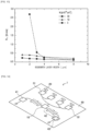
- FIG. 4 is a graph chart illustrating correlativeness between a density Ns of an electron traveling in a channel and third-order harmonic distortion of a series transistor.
- FIG. 5 is a scatter diagram illustrating a correspondence relation between an electron mobility and an electron density in an Si-based MOSFET and a compound semiconductor HEMT usable in a switching transistor.
- FIG. 6 is a graph chart illustrating a difference in a shunt transistor characteristic with respect to a gate structure of an HEMT that uses AlInN.
- FIG. 7 is a schematic cross-sectional diagram explaining a configuration of a switching transistor according to the embodiment of the present disclosure.
- FIG. 8 A is a schematic cross-sectional diagram illustrating an example of a substrate used in the switching transistor according to the embodiment.
- FIG. 8 B is a schematic cross-sectional diagram illustrating an example of a substrate used in the switching transistor according to the embodiment.
- FIG. 8 C is a schematic cross-sectional diagram illustrating an example of a substrate used in the switching transistor according to the embodiment.
- FIG. 9 A is a schematic cross-sectional diagram illustrating an example of a gate structure used in the switching transistor according to the embodiment.
- FIG. 9 B is a schematic cross-sectional diagram illustrating an example of a gate structure used in the switching transistor according to the embodiment.
- FIG. 9 C is a schematic cross-sectional diagram illustrating an example of a gate structure used in the switching transistor according to the embodiment.
- FIG. 10 A is a schematic cross-sectional diagram illustrating an example of a contact structure used in the switching transistor according to the embodiment.
- FIG. 10 B is a schematic cross-sectional diagram illustrating an example of a contact structure used in the switching transistor according to the embodiment.
- FIG. 10 C is a schematic cross-sectional diagram illustrating an example of a contact structure used in the switching transistor according to the embodiment.
- FIG. 11 is a graph chart illustrating a Transfer characteristic of the switching transistor illustrated in FIG. 7 .
- FIG. 12 is a graph chart illustrating an evaluation result of a third-order harmonic distortion characteristic of the switching transistor illustrated in FIG. 7 .
- FIG. 14 is a schematic perspective view explaining a semiconductor module to which the switching transistor according to the embodiment is applied.
- FIG. 1 is a schematic diagram explaining an application example of a switching transistor according to an embodiment of the present disclosure.
- a multitude of high frequency switches are provided for switching of an RF (Radio Frequency) signal.
- a high frequency switch is provided at a front end of the portable communication terminal.
- the high frequency switch allocates RF signals from an antenna ANT to a plurality of input/output ports.
- the high frequency switch illustrated in FIG. 1 is a SP10T (Single Pole 10 Through: single-pole-ten-throw) switch.
- the high frequency switch illustrated in FIG. 1 includes one pole coupled to the antenna ANT, 10 input/output ports that receive the RF signals from the antenna ANT, and one contact that switches ON or OFF between the one pole and the 10 input/output ports. It is possible to configure such a high frequency switch by a switching transistor, for example.
- the switching transistor to be used in such a high frequency switch is requested to have low loss from a standpoint of reducing power consumption of a portable communication terminal in which the switching transistor is to be mounted.
- CA Carrier Aggregation
- the plurality of frequency bands is bundled into one. Consequently, the plurality of frequency bands influences each other, thus resulting in a reduction in the transmission capacitance in some cases.
- a frequency band of 700 MHz and a frequency band of 2.1 GHz are bundled by means of the CA, a third-order harmonic of 700 MHz becomes a noise source for the 2.1 GHz. Therefore, the transmission capacitance decreases due to the noise in some cases.
- the switching transistor for a high frequency switch application to be mounted in the portable communication terminal it has been requested to further suppress harmonic distortion.
- the number of frequency bands to be used in the CA has been on the rise, and a switching transistor with lower distortion has been requested.
- the switching transistor for the high frequency switch application to be mounted in the portable communication terminal has been requested to have lower loss and lower distortion.
- Examples of such a switching transistor for the high frequency switch application may include a silicon (Si)-based MOSFET (Metal-Oxide-Semiconductor Field-Effect Transistor). Specifically, to suppress influence of an Si substrate that causes a parasitic capacitance, the MOSFET provided on an SOI (Silicon On Insulator) substrate is used as the switching transistor.
- Si silicon
- MOSFET Metal-Oxide-Semiconductor Field-Effect Transistor
- a MOSFET-type switching transistor 900 is provided on the SOI substrate in which a substrate 931 , a BOX layer 933 , and a semiconductor layer 935 are stacked in sequence.
- the substrate 931 is a silicon substrate, for example.
- the BOX layer 933 is a silicon oxide layer.
- the semiconductor layer 935 is a silicon layer.
- the SOI substrate may be formed, for example, by ion implanting oxygen molecules into an inside of the silicon substrate and oxidizing the silicon substrate to make it the BOX layer 933 .
- the SOI substrate may be formed, for example, by bonding together a carrier wafer on which the BOX layer 933 and the semiconductor layer 935 are formed, and the substrate 931 , and then peeling off the carrier wafer.
- a gate electrode 910 is provided on the semiconductor layer 935 via a gate insulating film 911 .
- the gate electrode 910 may include polysilicon, or the like, for example.
- the gate insulating film 911 may include silicon oxide (SiO 2 ), for example.
- a second conductivity type impurity is introduced to the semiconductor layer 935 .
- the second conductivity type impurity is a p-type impurity such as boron or aluminum, for example.
- introduction of a first conductivity type impurity to the semiconductor layer 935 on both sides of the gate electrode 910 forms a source region 935 S and a drain region 935 D.
- the first conductivity type impurity is an n-type impurity such as phosphorus or arsenic, for example.
- a source contact 920 S and a drain contact 920 D are provided on the source region 935 S and the drain region 935 D, respectively.
- the source contact 920 S and the drain contact 920 D may include a conductive material such as tungsten, titanium, aluminum, or copper, for example.
- the switching transistor 900 is denoted as an equivalent circuit including on-resistance R on ( ⁇ mm) when being on.
- the on-resistance R on may be generated, for example, due to continuity resistance R sd of a channel between the source region 935 S and the drain region 935 D, contact resistance Rc between the source contact 920 S and the drain contact 920 D, and the source region 935 S and the drain region 935 D, diffusion resistance of the source region 935 S and the drain region 935 D, and the like.
- the switching transistor 900 is denoted as the equivalent circuit including off-capacitance C off (C/mm) when being off.
- the off-capacitance C off may be generated, for example, by capacitances C gs and C gd between the source region 935 S and the drain region 935 D, and the gate electrode 910 , a capacitance C ds between the source region 935 S and the drain region 935 D, capacitances C bs and C bd via a depletion layer between the source region 935 S and the drain region 935 D, and the semiconductor layer 935 , and the like.
- a figure of merit (FoM) (second) of the switching transistor 900 is defined as a product of the above-described on-resistance R on ( ⁇ mm) and the off-capacitance C off (C/mm). It may be said that the switching transistor 900 is a switching transistor which has lower loss as the FoM is smaller.
- FIG. 3 is a graph chart schematically illustrating a correlation between a gate length of the switching transistor 900 , and R on , C off , and R on *C off .
- the MOSFET type switching transistor 900 formed on the SOI substrate aims to improve the FoM, for example, through the use of a decrease in the on-resistance R on due to miniaturization, a decrease in the off-capacitance C off due to provision of multiple stages attributable to a smaller device size, a decrease in the capacitances C bs and C bd due to a change from a PD-SOI (Partially-Depleted-SOI) to an FD-SOI (Fully-Depleted SO1), and the like.
- PD-SOI Partially-Depleted-SOI
- FD-SOI Full-Depleted SO1
- examples of the switching transistor for the high frequency switch application other than the Si-based MOSFET may include a high electron mobility transistor (High Electron Mobility Transistor: HEMT).
- HEMT High Electron Mobility Transistor
- the HEMT is a field-effect transistor that uses, as a channel, a two-dimensional electron gas with a high mobility induced by a semiconductor hetero-junction.
- the HEMT is, in general, formed by the hetero-junction of a compound semiconductor.
- GaAs-based HEMT InGaAs, which are each the compound semiconductor, form a hetero-junction
- a channel having an electron travelling is formed in an InGaAs layer.
- Such a GaAs-based HEMT exhibits the high electron mobility that is 6 times or higher with respect to the Si-based MOSFET. Consequently, it is possible to achieve extremely low sheet resistance and lower the on-resistance R on extremely.
- the GaAs-based HEMT it is not easy to promote reduction of a device size due to a restriction by an ohmic characteristic and it has been difficult to reduce the off-capacitance C off by reducing the device size. Therefore, the GaAs-based HEMT aims to improve the FoM by applying a large gate off voltage and reducing the off-capacitance C off .
- the present inventors have diligently reviewed the transistor with the low loss and the low distortion suitable as the switching transistor for the high frequency switch application. As a result, the present inventors have arrived at findings to be described below and have completed the technology according to the present disclosure. In the following, description is given of the technology according to the present disclosure, with reference to FIG. 4 to FIG. 6 .
- the present inventors have found that in the switching transistor, there is correlativeness between the density of the electron travelling in the channel and the third-order harmonic distortion of the series transistor.
- the decrease in the on-resistance R on that is, the decrease in the sheet resistance of the channel is important to achieve the low loss and the low distortion.
- the sheet resistance is determined by the density of the electron travelling in the channel and the electron mobility, and bears such a relationship that as the electron density becomes higher, the electron mobility decreases.
- the present inventors have reviewed the correspondence relation between the electron density Ns and the third-order harmonic distortion with the sheet resistance fixed, and have found that there is favorable correlativeness between the electron density Ns and the third-order harmonic distortion.
- FIG. 4 is a graph chart illustrating the correlativeness between the density Ns of the electron traveling in the channel and the third-order harmonic distortion of the series transistor.
- the electron density Ns is same, the higher electron mobility makes it possible to improve the characteristic such as the on-resistance R on , but the electron mobility has a smaller range of fluctuation than the electron density Ns. Therefore, it is believed that performing the device design giving importance to the electron density that allows for improvement of the high frequency characteristic makes it possible to implement the switching transistor that is more suitable for the high frequency application.
- FIG. 5 is a scatter diagram illustrating the correspondence relation between the electron mobility and the electron density in the Si-based MOSFET and the compound semiconductor usable in the switching transistor. It is to be noted that the dashed lines in FIG. 5 are lines that indicate identical sheet resistance.
- a filled triangle represents a plot of a laminated body of InAlAs/InGaAs and a white outlined circle represents a plot of a laminated body of AlGaAs/InGaAs.
- a double circle represents a plot of a laminated body of AlGaN/GaN.
- a white outlined square represents a plot of a laminated body of AlGaInN/GaN/SiC
- a filled square represents a plot of a laminated body of AlInN/GaN/Sapphire
- a filled diamond shape represents a plot of a laminated body of AlInN/GaN/Si.
- the HEMT using GaAs and the like has the low electron density Ns of 3 to 4 ⁇ 10 12 cm ⁇ 2 although it has the favorable electron mobility (electron transfer characteristic).
- the Si-based MOSFET Si MOS
- the high electron density Ns of 1 ⁇ 10 13 cm ⁇ 2 although it has the low electron mobility.
- a GaN-based material has the higher electron density than GaAs, etc.
- AlGaInN/GaN is a system that makes it possible to form the switching transistor for the high frequency application with the desired low loss and low distortion, because AlGaInN/GaN has the low sheet resistance of 200 ⁇ / ⁇ and has the high electron density Ns equal to or higher than 1.7 ⁇ 10 13 cm ⁇ 2 and the high electron mobility.
- the switching transistor according to the present embodiment is the HEMT including a barrier layer and a channel layer that form a semiconductor hetero-junction and having the sheet electron density of the channel layer that is equal to or higher than 1.7 ⁇ 10 13 cm ⁇ 2 .
- a leak characteristic between the barrier layer including AlGaInN and the gate electrode and the ohmic characteristic of coupling to the channel layer via the barrier layer may not be favorable in some cases.
- a shunt characteristic of the transistor degrades.
- the ohmic characteristic of coupling to the channel layer via the barrier layer it becomes difficult to achieve a desired switching characteristic.
- FIG. 6 is a graph chart illustrating the difference in the shunt transistor characteristic with respect to the gate structure of the HEMT that uses AlInN.
- the present inventors have found that for the degradation of the ohmic characteristic of the transistor, a contact of the barrier layer with an electrode of each terminal causes the degradation of the ohmic characteristic. Hence, the present inventors have discovered that improvement of the contact of the barrier layer of the HEMT with the electrode of each terminal makes it possible to achieve the more favorable switching characteristic.
- FIG. 7 is a schematic cross-sectional diagram explaining the configuration of the switching transistor according to the present embodiment.
- a switching transistor 100 includes a support substrate 130 , a channel layer 131 , a spacer layer 133 , a barrier layer 135 , a protection layer 137 , ohmic metal layers 121 , source or drain electrodes 120 , an insulation layer 117 , a gate insulating film 111 , and a gate electrode 110 .
- the support substrate 130 is a substrate that supports each component of the switching transistor 100 .
- the support substrate 130 may be, for example, a substrate including a III-V compound semiconductor material and may be, for example, a single-crystalline gallium nitride (GaN) substrate having semi-insulation properties.
- GaN gallium nitride
- a material that the support substrate 130 includes is not limited in particular.
- the support substrate 130 may be a silicon (Si) substrate, a silicon carbide (SiC) substrate, a sapphire substrate, or the like.
- the channel layer 131 includes a compound semiconductor material and is provided on the support substrate 130 .
- the electron travels due to the semiconductor hetero-junction with the barrier layer 135 , to be described later, and the two-dimensional electron gas serving as the channel is formed.
- the channel layer 131 may include GaN, for example, and may include InGaN or AlGaN.
- a buffer layer may be provided between the channel layer 131 and the support substrate 130 to alleviate a difference between a lattice constant of the support substrate 130 and that of the channel layer 131 .
- the buffer layer may include a material having a lattice constant that is intermediate between the lattice constant of the material that the channel layer 131 includes and the lattice constant of a material that the support substrate 130 includes. Provision of the appropriate buffer layer makes a crystal state of the channel layer 131 favorable and suppresses overall warping of the switching transistor 100 .
- the barrier layer 135 includes a compound semiconductor material that is of a different type from the channel layer 131 , and is provided on the channel layer 131 .
- the barrier layer 135 accumulates the electron in the channel layer 131 by the hetero-junction with the channel layer 131 and forms the two-dimensional electron gas in the channel layer 131 .
- the barrier layer 135 may include Al 1-x-y Ga x In y N (where 0 ⁇ x ⁇ 1, 0 ⁇ y ⁇ 1, 0 ⁇ x+y ⁇ 1).
- the compound semiconductor materials that the channel layer 131 and the barrier layer 135 include are selected so that the sheet electron density of the channel layer 131 is equal to or higher than 1.7 ⁇ 10 13 cm ⁇ 2 . That is, as described above, the channel layer 131 may include GaN and the barrier layer 135 may include Al 1-x-y Ga x In y N (where 0 ⁇ x ⁇ 1, 0 ⁇ y ⁇ 1, 0 ⁇ x+y ⁇ 1). In such a case, the channel layer 131 and the barrier layer 135 make it possible to cause the two-dimensional electron gas formed in the channel layer 131 to have the sheet electron density equal to or higher than 1.7 ⁇ 10 13 cm ⁇ 2 .
- the sheet electron density of the two-dimensional electron gas formed in the channel layer 131 be equal to or higher than 1.7 ⁇ 10 13 cm ⁇ 2
- types of the respective compound semiconductor materials that form the channel layer 131 and the barrier layer 135 are not limited to the above-described combination.
- the spacer layer 133 is provided so as to be inserted between the barrier layer 135 and the channel layer 131 .
- the spacer layer 133 includes a compound semiconductor material having larger polarization than the barrier layer 135 and improves the electron mobility of the two-dimensional electron gas formed in the channel layer 131 .
- the spacer layer 133 may include AlN, for example.
- the spacer layer 133 may include InGaN, AlGaN, or the like.
- the protection layer 137 includes an insulating material and is provided on the barrier layer 135 of a region where the gate electrode 110 , and the source or drain electrode 120 are not provided.
- the protection layer 137 is provided to protect the barrier layer 135 from an impurity such as ion in a manufacturing process of the switching transistor 100 .
- the protection layer 137 is removed in the region where the gate electrode 110 and the source or the drain electrode 120 are provided, as these electrodes are formed.
- the protection layer 137 may include the insulating material such as GaN, SiO 2 , SiN, or Al 2 O 3 , for example.
- the insulation layer 117 includes an insulating material and is provided on the barrier layer 135 .
- the insulation layer 117 electrically insulates the barrier layer 135 from an electrode, a wiring line, or the like. However, on the insulation layer 117 , an opening is provided that corresponds to the region where the gate electrode 110 and the source or drain electrode 120 are provided. This allows the gate electrode 110 and the source or drain electrode 120 to electrically contact the barrier layer 135 .
- the insulation layer 117 may be formed as a single-layer film or a laminated film of the insulating material such as SiO 2 , SiN, or Al 2 O 3 , for example.
- the gate insulating film 111 includes a dielectric material having the insulation properties and is provided on the barrier layer 135 . Specifically, the gate insulating film 111 may be provided uniformly over the barrier layer 135 and the insulation layer 117 .
- the gate insulating film 111 may include an oxide such as SiO 2 , Al 2 O 3 , or HfO 2 or a nitride such as SiN, AlN, or BN.
- the gate electrode 110 includes a conductive material and is provided on the gate insulating film 111 . Specifically, the gate electrode 110 may be provided on the opening provided on the insulation layer 117 , so as to contact the barrier layer 135 via the gate insulating film 111 .
- the gate electrode 110 may include the single-layer film or the laminated film of Ti, Al, Ni, Au, or the like, for example.
- the ohmic metal layer 121 includes a conductive material and is provided on the barrier layer 135 . By forming an ohmic junction with the barrier layer 135 , the ohmic metal layer 121 reduces the contact resistance between the source or drain electrode 120 and the two-dimensional electron gas (channel) formed in the channel layer 131 .
- the ohmic metal layer 121 may include the single-layer film or the laminated film of metal having a small work function, such as Ti, Al, Ni, or Au, for example. Because the ohmic metal layer 121 allows for improvement of the ohmic characteristic between the source or drain electrode 120 and the barrier layer 135 , it is possible to improve the switching characteristics of the switching transistor 100 .
- the source or drain electrode 120 includes a conductive material and is provided on the ohmic metal layer 121 .
- the source or drain electrode 120 contacts the two-dimensional electron gas (channel) formed in the channel layer 131 , via the ohmic metal layer 121 .
- the source or drain electrode 120 may include a general wiring line material such as Cu or Al, for example. It is to be noted that the source or drain electrodes 120 are provided on both sides with the gate electrode 110 interposed therebetween, and one is the source electrode and the other the drain electrode.
- the switching transistor 100 it is possible for the switching transistor 100 to improve the shunt transistor characteristic by including the MIS gate structure. Furthermore, by including the ohmic metal layer 121 , the switching transistor 100 allows for the improvement of the ohmic characteristic between the source or drain electrode 120 and the barrier layer 135 , thus making it possible to improve the switching characteristics.
- Formation of the switching transistor 100 according to the present embodiment is possible by repeating film formation by means of sputtering or CVD (Chemical Vapor Deposition), patterning by means of photolithography and etching, and the like. It is to be noted that ALD (Atomic Layer Deposition), in particular, may be used to form a film. It is possible to use the ALD suitably in forming the switching transistor 100 according to the present embodiment because the ALD allows a favorable interface to be obtained on an insulating film or a semiconductor.
- CVD Chemical Vapor Deposition
- FIGS. 8 A, 8 B, and 8 C are each a schematic cross-sectional diagram illustrating an example of the substrate to be used in the switching transistor 100 according to the present embodiment.
- the switching transistor 100 may be formed by means of a substrate where the support substrate 130 , the channel layer 131 , the spacer layer 133 , the barrier layer 135 , and the protection layer 137 are stacked in sequence. It is to be noted that the configurations of these are as described above, and thus description thereof is omitted here.
- the switching transistor 100 it is possible to form the switching transistor 100 by means of the substrate illustrated in FIG. 8 B , as described below. Specifically, first, the protection layer 137 of the region corresponding to the gate electrode 110 and the source or drain electrode 120 is removed by etching. Next, after the films of the ohmic metal layer 121 and the insulation layer 117 are formed on the substrate illustrated in FIG. 8 B , openings are provided on the insulation layer 117 of the region corresponding to the gate electrode 110 and the source or drain electrode 120 . Thereafter, the gate insulating film 111 is formed on the insulation layer 117 , and the gate electrode 110 and the source or drain electrode 120 are formed on the respective openings provided on the insulation layer 117 . This allows for the formation of the switching transistor 100 .
- the substrate illustrated in FIG. 8 B allows for protection of the barrier layer 135 by the protection layer 137 . Therefore, it is possible to suppress degradation of the characteristic of the barrier layer 135 due to entry of the impurity such as ion and resulting degradation of the characteristics of the switching transistor 100 .
- the switching transistor 100 may be formed by means of a substrate where the support substrate 130 , the channel layer 131 , the spacer layer 133 , and the barrier layer 135 are stacked in sequence and a back-barrier layer 139 is inserted into an inside of the channel layer 131 .
- the back-barrier layer 139 includes a compound semiconductor material, and is provided to be inserted into the barrier layer 135 side inside the channel layer 131 .
- the back-barrier layer 139 includes the compound semiconductor material that is similar to the barrier layer 135 .
- the barrier layer 135 includes Al 1-x-y Ga x In y N (where 0 ⁇ x ⁇ 1, 0 ⁇ y ⁇ 1, 0 ⁇ x+y ⁇ 1)
- the back-barrier layer 139 may similarly include Al 1-x-y Ga x In y N (where 0 ⁇ x ⁇ 1, 0 ⁇ y ⁇ 1, 0 ⁇ x+y ⁇ 1). It is to be noted that other configurations are as described above, and thus description thereof is omitted here.
- the switching transistor 100 it is possible to form the switching transistor 100 by means of the substrate illustrated in FIG. 8 C , as described below. Specifically, first, after the films of the ohmic metal layer 121 and the insulation layer 117 are formed on the substrate illustrated in FIG. 8 C , openings are provided on the insulation layer 117 of the region corresponding to the gate electrode 110 and the source or drain electrode 120 . Thereafter, the gate insulating film 111 is formed on the insulation layer 117 , and the gate electrode 110 and the source or drain electrode 120 are formed on the respective openings provided on the insulation layer 117 . This allows for the formation of the switching transistor 100 .
- provision of the back-barrier layer 139 makes it possible to suppress a short-gate effect.
- FIGS. 9 A, 9 B, and 9 C are each a schematic cross-sectional diagram illustrating an example of the gate structure to be used in the switching transistor according to the present embodiment.
- a gate structure of a switching transistor 100 B may be the MIS gate structure in which the gate electrode 110 is provided on the barrier layer 135 via a first gate insulating film 112 B and a second gate insulating film 113 B. That is, in the switching transistor 100 B, the gate insulating film may include the laminated film.
- the first gate insulating film 112 B and the second gate insulating film 113 B may be, for example, the oxide film including SiO 2 , Al 2 O 3 , HfO 2 , BeO, or the like or the nitride film including SiN, Si 2 N 3 , AlN, BN, or the like which are described above as the material of the oxide film or nitride film 111 A illustrated in FIG. 9 A .
- the gate insulating film may include the laminated film in which two or more types of the oxide films or the nitride films are stacked.
- the gate structure of a switching transistor 100 C may be the MIS gate structure in which the gate electrode 110 is provided on the barrier layer 135 via an intermediate layer 114 C and a gate insulating film 111 C.
- the intermediate layer 114 C is provided between the barrier layer 135 and the gate insulating film 111 C to improve an interface characteristic of the MIS gate structure.
- the intermediate layer 114 C may include Si or Ge, for example, and may include other insulating material or non-insulating material as far as it improves the interface characteristic of the MIS gate structure.
- FIGS. 10 A, 10 B, and 10 C are each a schematic cross-sectional diagram illustrating an example of a contact structure to be used in the switching transistor according to the present embodiment.
- doping regions 122 are provided in the barrier layer 135 under the ohmic metal layers 121 .
- the doping region 122 is provided by doping, with a conductive impurity to high density, the region of the barrier layer 135 under each ohmic metal layer 121 that is provided under the source or drain electrode 120 .
- the doping region 122 may be formed as an n-type region having the high density, in a partial region of the barrier layer 135 . After this, by the ohmic metal layer 121 being formed on the doping region 122 of the barrier layer 135 , it is possible to form the switching transistor 101 A.
- provision of the doping region 122 with improved electric conductivity in the barrier layer 135 under the ohmic metal layer 121 makes it possible to further reduce the contact resistance between the ohmic metal layer 121 and the barrier layer 135 .
- the ohmic metal layer 121 is provided to be in direct contact with the channel layer 131 in which the two-dimensional electron gas, which is the channel, is formed. Therefore, it is possible to further reduce the on-resistance of the switching transistor 101 B.
- the barrier layer 135 and the spacer layer 133 of the region corresponding to the source or drain electrode 120 is removed by the etching and an opening that exposes the channel layer 131 is formed on the barrier layer 135 .
- the ohmic regrowth layer 123 is formed on the opening of the barrier layer 135 , by causing GaInN or GaN, which is doped with the n-type having the high density, to regrow. Thereafter, by the ohmic metal layer 121 and the source or drain electrode 120 being formed on the ohmic regrowth layer 123 , the switching transistor 101 C is formed.
- the source or drain electrode 120 it is possible for the source or drain electrode 120 to reduce the contact resistance with the channel layer 131 by intervention of the ohmic metal layer 121 and the ohmic regrowth layer 123 .
- FIGS. 10 A, 10 B, and 10 C it is possible for the contact structure illustrated in FIG. 10 C to achieve the most favorable ohmic characteristic.
- FIG. 11 is a graph chart illustrating a DC (Direct Current) characteristic of the switching transistor 100 illustrated in FIG. 7 .
- FIG. 11 is a graph chart illustrating the Transfer characteristic of the switching transistor 100 illustrated in FIG. 7 .
- the switching transistor 100 As illustrated in FIG. 11 , the switching transistor 100 according to the present embodiment exhibits a low off-current value and it is seen that a leak current is little. In addition, the switching transistor 100 exhibits a steep rising characteristic near a threshold voltage and it is seen that the switching transistor 100 has the favorable switching characteristic.
- FIG. 12 is a graph chart illustrating an evaluation result of a third-order harmonic distortion characteristic of the switching transistor 100 illustrated in FIG. 7 .
- the dashed lines represent estimated values from a simulation
- a filled circle is a plot of an actually measured value using a substrate having the sheet electron density Ns of 1.6 ⁇ 10 13 cm ⁇ 2 .
- the actually measured value is substantially consistent with a simulation result. Therefore, it is seen that the switching transistor 100 according to the present embodiment allows for reduction of the harmonic distortion.
- FIG. 13 is a graph chart illustrating a relation between the size of the ohmic regrowth layer 123 and the ohmic characteristic of the switching transistor 101 C illustrated in FIG. 10 C .
- adoption of the contact structure of the switching transistor 101 C illustrated in FIG. 10 C makes it possible to lower the ohmic resistance extremely.
- the sheet electron density Ns be 1.7 ⁇ 10 13 cm ⁇ 2
- the on-resistance R on be equal to or lower than 0.4 ⁇ mm
- the ohmic resistance be equal to or lower than 0.1 ⁇ mm.
- the adoption of the contact structure illustrated in FIG. 10 C makes it possible to achieve the ohmic resistance that is equal to or lower than 0.1 ⁇ mm.
- the size of the ohmic regrowth layer 123 is also a parameter that contributes to the shunt transistor characteristic. As the size of the ohmic regrowth layer 123 becomes smaller, the shunt transistor characteristic improves. In contrast, as the size of the ohmic regrowth layer 123 becomes smaller, the ohmic resistance increases. Therefore, conditions for forming the ohmic regrowth layer 123 that satisfies both of the shunt transistor characteristic and the ohmic resistance are requested. With reference to the result of FIG.
- the ohmic regrowth layer 123 if it is subjected to the n-type doping with the density equal to or higher than 3 ⁇ 10 20 cm ⁇ 3 and has the size equal to or larger than 3 ⁇ m, makes it possible to achieve the above-described desired characteristics.
- FIG. 14 is a schematic perspective view explaining the semiconductor module to which the switching transistor 100 according to the present embodiment is applied.
- a semiconductor module 1 includes, for example, an edge antenna 20 , a driver 31 , a phase adjustment circuit 32 , a switch 10 , a low-noise amplifier 41 , a bandpass filter 42 , and a power amplifier 43 .
- the semiconductor module 1 is an antenna-integrated-module in which the array-like formed edge antenna 20 , and front-end components such as the switch 10 , the low-noise amplifier 41 , the bandpass filter 42 , and the power amplifier 43 are integrally mounted as one module.
- Such a semiconductor module 1 may be used as a communication transceiver, for example.
- the switching transistor 100 according to the present embodiment may be applied to the switch 10 , for example.
- Use of the switching transistor 100 according to the present embodiment makes it possible to implement the switch 10 for the high frequency application that achieves the low loss and the low distortion requested as the communication transceiver.
- a switching transistor including:
- a channel layer including a compound semiconductor and having sheet electron density that is equal to or higher than 1.7 ⁇ 10 13 cm ⁇ 2 ;
- a source electrode and a drain electrode provided on the barrier layer with the gate electrode interposed between the source electrode and the drain electrode.
- the switching transistor according to (1) in which the gate electrode is provided on the barrier layer via a gate insulating film.
- the switching transistor according to (2) in which the gate insulating film includes a film including an oxide or a nitride.
- the switching transistor according to (4) in which a spacer layer is further provided on an interface between the channel layer and the barrier layer.
- a regrowth layer is further provided under the ohmic metal layer, the regrowth layer including a compound semiconductor containing a conductivity type impurity, and
- the regrowth layer is provided to penetrate through the barrier layer to be in contact with the channel layer.
- the regrowth layer is provided in a planar shape having a minimum width that is equal to or larger than 3 ⁇ m, and
- an amount of the conductivity type impurity contained by the regrowth layer is equal to or larger than 3 ⁇ 10 20 cm ⁇ 3 .
- the switching transistor according to (7) in which the ohmic metal layer is provided to penetrate through the barrier layer to be in contact with the channel layer.
- the switching transistor according to (7) in which a doping region including a conductivity type impurity is formed in the barrier layer under the ohmic metal layer.
- a semiconductor module including:
- a switching transistor provided on the substrate and coupled to the various types of amplifiers, in which
- the switching transistor includes
Landscapes
- Engineering & Computer Science (AREA)
- Computer Hardware Design (AREA)
- Physics & Mathematics (AREA)
- Condensed Matter Physics & Semiconductors (AREA)
- General Physics & Mathematics (AREA)
- Manufacturing & Machinery (AREA)
- Junction Field-Effect Transistors (AREA)
- Microelectronics & Electronic Packaging (AREA)
- Power Engineering (AREA)
- Electrodes Of Semiconductors (AREA)
- Internal Circuitry In Semiconductor Integrated Circuit Devices (AREA)
- Thin Film Transistor (AREA)
- Insulated Gate Type Field-Effect Transistor (AREA)
Abstract
Description
- PTL 1: Japanese Unexamined Patent Application Publication No. 2015-207639
-
- a channel layer including a compound semiconductor and having sheet electron density that is equal to or higher than 1.7×1013 cm−2,
- a barrier layer formed on the channel layer by using a compound semiconductor that is of a different type from the channel layer,
- a gate electrode provided on the barrier layer, and
- a source electrode and a drain electrode provided on the barrier layer with the gate electrode interposed between the source electrode and the drain electrode.
- 1 Semiconductor module
- 10 Switch
- 20 Edge antenna
- 31 Driver
- 32 Phase adjustment circuit
- 41 Low-noise amplifier
- 42 Bandpass filter
- 43 Power amplifier
- 100 Switching transistor
- 110 Gate electrode
- 111 Gate insulating film
- 117 Insulation layer
- 120 Source or drain electrode
- 121 Ohmic metal layer
- 130 Support substrate
- 131 Channel layer
- 133 Spacer layer
- 135 Barrier layer
- 137 Protection layer
Claims (13)
Applications Claiming Priority (4)
| Application Number | Priority Date | Filing Date | Title |
|---|---|---|---|
| JP2018-086845 | 2018-04-27 | ||
| JP2018086845A JP2021120966A (en) | 2018-04-27 | 2018-04-27 | Switching transistor and semiconductor module |
| JPJP2018-086845 | 2018-04-27 | ||
| PCT/JP2019/011679 WO2019208034A1 (en) | 2018-04-27 | 2019-03-20 | Switching transistor and semiconductor module |
Publications (2)
| Publication Number | Publication Date |
|---|---|
| US20210111277A1 US20210111277A1 (en) | 2021-04-15 |
| US11682720B2 true US11682720B2 (en) | 2023-06-20 |
Family
ID=68294534
Family Applications (1)
| Application Number | Title | Priority Date | Filing Date |
|---|---|---|---|
| US17/047,453 Active 2039-07-06 US11682720B2 (en) | 2018-04-27 | 2019-03-20 | Switching transistor and semiconductor module to suppress signal distortion |
Country Status (3)
| Country | Link |
|---|---|
| US (1) | US11682720B2 (en) |
| JP (1) | JP2021120966A (en) |
| WO (1) | WO2019208034A1 (en) |
Families Citing this family (5)
| Publication number | Priority date | Publication date | Assignee | Title |
|---|---|---|---|---|
| CN115668506A (en) * | 2020-05-25 | 2023-01-31 | 索尼半导体解决方案公司 | Semiconductor device, semiconductor module, and electronic apparatus |
| WO2022049983A1 (en) * | 2020-09-01 | 2022-03-10 | ソニーグループ株式会社 | Semiconductor device, semiconductor module, and wireless communication device |
| CN117546301A (en) * | 2021-06-30 | 2024-02-09 | 索尼集团公司 | Semiconductor device, semiconductor module, and wireless communication apparatus |
| US20240194751A1 (en) * | 2022-12-09 | 2024-06-13 | Wolfspeed, Inc. | Transistor devices including self-aligned ohmic contacts and contact regions and related fabrication methods |
| CN119584577B (en) * | 2024-11-21 | 2025-12-02 | 西安电子科技大学 | AlN-based RF power transistors with high thermal conductivity BeO passivation and their fabrication method |
Citations (16)
| Publication number | Priority date | Publication date | Assignee | Title |
|---|---|---|---|---|
| WO2006022453A1 (en) | 2004-08-27 | 2006-03-02 | National Institute Of Information And Communications Technology, Incorporated Administrative Agency | GaN-BASED FIELD EFFECT TRANSISTOR AND PRODUCTION METHOD THEREFOR |
| US20060108606A1 (en) * | 2004-11-23 | 2006-05-25 | Saxler Adam W | Cap layers and/or passivation layers for nitride-based transistors, transistor structures and methods of fabricating same |
| JP2008235613A (en) | 2007-03-22 | 2008-10-02 | Eudyna Devices Inc | Semiconductor device |
| JP2009302370A (en) | 2008-06-16 | 2009-12-24 | Nippon Telegr & Teleph Corp <Ntt> | Semiconductor device |
| US20100038682A1 (en) * | 2007-03-30 | 2010-02-18 | Lahreche Hacene | Electronic devices with improved ohmic contact |
| US20100270559A1 (en) * | 2007-11-19 | 2010-10-28 | Nec Corporation | Field effect transistor and process for manufacturing same |
| US20110127604A1 (en) * | 2009-11-30 | 2011-06-02 | Ken Sato | Semiconductor device |
| JP2011159795A (en) | 2010-02-01 | 2011-08-18 | Nippon Telegr & Teleph Corp <Ntt> | Semiconductor device and method of fabricating the same |
| JP2012049216A (en) | 2010-08-25 | 2012-03-08 | Mitsubishi Electric Corp | Manufacturing method of heterojunction field effect transistor |
| US20140327047A1 (en) * | 2013-05-03 | 2014-11-06 | Texas Instruments Incorporated | Fet dielectric reliability enhancement |
| DE102015000190A1 (en) | 2014-01-16 | 2015-07-16 | Triquint Semiconductor, Inc. | Doped gallium nitride transistor with high electron mobility |
| JP2015207639A (en) | 2014-04-18 | 2015-11-19 | ソニー株式会社 | Semiconductor device for high frequency switch, high frequency switch and high frequency module |
| WO2016068935A1 (en) | 2014-10-30 | 2016-05-06 | Intel Corporation | Source/drain regrowth for low contact resistance to 2d electron gas in gallium nitride transistors |
| US20160225857A1 (en) * | 2015-02-04 | 2016-08-04 | Kabushiki Kaisha Toshiba | Semiconductor device and method for manufacturing the same |
| US20170125545A1 (en) * | 2015-10-30 | 2017-05-04 | Fujitsu Limited | Compound semiconductor device and manufacturing method thereof |
| JP2018064027A (en) | 2016-10-13 | 2018-04-19 | 富士通株式会社 | Compound semiconductor device, and method for manufacturing the same |
-
2018
- 2018-04-27 JP JP2018086845A patent/JP2021120966A/en active Pending
-
2019
- 2019-03-20 US US17/047,453 patent/US11682720B2/en active Active
- 2019-03-20 WO PCT/JP2019/011679 patent/WO2019208034A1/en not_active Ceased
Patent Citations (31)
| Publication number | Priority date | Publication date | Assignee | Title |
|---|---|---|---|---|
| WO2006022453A1 (en) | 2004-08-27 | 2006-03-02 | National Institute Of Information And Communications Technology, Incorporated Administrative Agency | GaN-BASED FIELD EFFECT TRANSISTOR AND PRODUCTION METHOD THEREFOR |
| EP1801865A1 (en) | 2004-08-27 | 2007-06-27 | National Institute of Information and Communications Technology Incorporated Administrative Agency | GaN-BASED FIELD EFFECT TRANSISTOR AND PRODUCTION METHOD THEREFOR |
| US20070295990A1 (en) | 2004-08-27 | 2007-12-27 | National Institute Of Information And Communications Technology, Incorporated Adm | Gan-Based Field Effect Transistor and Production Method Therefor |
| US20060108606A1 (en) * | 2004-11-23 | 2006-05-25 | Saxler Adam W | Cap layers and/or passivation layers for nitride-based transistors, transistor structures and methods of fabricating same |
| JP2008235613A (en) | 2007-03-22 | 2008-10-02 | Eudyna Devices Inc | Semiconductor device |
| US20100038682A1 (en) * | 2007-03-30 | 2010-02-18 | Lahreche Hacene | Electronic devices with improved ohmic contact |
| US20100270559A1 (en) * | 2007-11-19 | 2010-10-28 | Nec Corporation | Field effect transistor and process for manufacturing same |
| JP2009302370A (en) | 2008-06-16 | 2009-12-24 | Nippon Telegr & Teleph Corp <Ntt> | Semiconductor device |
| US20110127604A1 (en) * | 2009-11-30 | 2011-06-02 | Ken Sato | Semiconductor device |
| JP2011159795A (en) | 2010-02-01 | 2011-08-18 | Nippon Telegr & Teleph Corp <Ntt> | Semiconductor device and method of fabricating the same |
| JP2012049216A (en) | 2010-08-25 | 2012-03-08 | Mitsubishi Electric Corp | Manufacturing method of heterojunction field effect transistor |
| US20140327047A1 (en) * | 2013-05-03 | 2014-11-06 | Texas Instruments Incorporated | Fet dielectric reliability enhancement |
| WO2014179809A1 (en) | 2013-05-03 | 2014-11-06 | Texas Instrument Incorporated | Gallium nitride field effect transistor |
| US20150060949A1 (en) | 2013-05-03 | 2015-03-05 | Texas Instruments Incorporated | Fet dielectric reliability enhancement |
| CN105164810A (en) | 2013-05-03 | 2015-12-16 | 德克萨斯仪器股份有限公司 | Gallium nitride field effect transistor |
| JP2016522991A (en) | 2013-05-03 | 2016-08-04 | 日本テキサス・インスツルメンツ株式会社 | Gallium nitride field effect transistor |
| EP2992557A1 (en) | 2013-05-03 | 2016-03-09 | Texas Instruments Incorporated | Gallium nitride field effect transistor |
| DE102015000190A1 (en) | 2014-01-16 | 2015-07-16 | Triquint Semiconductor, Inc. | Doped gallium nitride transistor with high electron mobility |
| JP2015135965A (en) | 2014-01-16 | 2015-07-27 | トライクイント・セミコンダクター・インコーポレイテッドTriQuint Semiconductor,Inc. | Doped gallium nitride high-electron mobility transistor |
| US20150200287A1 (en) * | 2014-01-16 | 2015-07-16 | Triquint Semiconductor, Inc. | Doped gallium nitride high-electron mobility transistor |
| JP2015207639A (en) | 2014-04-18 | 2015-11-19 | ソニー株式会社 | Semiconductor device for high frequency switch, high frequency switch and high frequency module |
| EP3213350A1 (en) | 2014-10-30 | 2017-09-06 | Intel Corporation | Source/drain regrowth for low contact resistance to 2d electron gas in gallium nitride transistors |
| WO2016068935A1 (en) | 2014-10-30 | 2016-05-06 | Intel Corporation | Source/drain regrowth for low contact resistance to 2d electron gas in gallium nitride transistors |
| JP2017539073A (en) | 2014-10-30 | 2017-12-28 | インテル・コーポレーション | Source / drain regrowth for low contact resistance to 2D electron gas in gallium nitride transistors |
| US20170278959A1 (en) | 2014-10-30 | 2017-09-28 | Intel Corporation | Source/drain regrowth for low contact resistance to 2d electron gas in gallium nitride transistor |
| CN106796953A (en) | 2014-10-30 | 2017-05-31 | 英特尔公司 | Low contact resistance regrowth of source/drain to 2D electron gas in GaN transistors |
| US20160225857A1 (en) * | 2015-02-04 | 2016-08-04 | Kabushiki Kaisha Toshiba | Semiconductor device and method for manufacturing the same |
| JP2017085060A (en) | 2015-10-30 | 2017-05-18 | 富士通株式会社 | Compound semiconductor device and manufacturing method thereof |
| US20170125545A1 (en) * | 2015-10-30 | 2017-05-04 | Fujitsu Limited | Compound semiconductor device and manufacturing method thereof |
| JP2018064027A (en) | 2016-10-13 | 2018-04-19 | 富士通株式会社 | Compound semiconductor device, and method for manufacturing the same |
| US20180108768A1 (en) | 2016-10-13 | 2018-04-19 | Fujitsu Limited | Compound semiconductor device and method of manufacturing compound semiconductor device |
Non-Patent Citations (1)
| Title |
|---|
| International Search Report and Written Opinion of PCT Application No. PCT/JP2019/011679, dated Jun. 18, 2019, 13 pages of ISRWO. |
Also Published As
| Publication number | Publication date |
|---|---|
| WO2019208034A1 (en) | 2019-10-31 |
| JP2021120966A (en) | 2021-08-19 |
| US20210111277A1 (en) | 2021-04-15 |
Similar Documents
| Publication | Publication Date | Title |
|---|---|---|
| US11682720B2 (en) | Switching transistor and semiconductor module to suppress signal distortion | |
| JP6554530B2 (en) | Group III nitride transistor using regrowth structure | |
| US9112010B2 (en) | Nitride-based semiconductor device | |
| US20130099284A1 (en) | Group iii-nitride metal-insulator-semiconductor heterostructure field-effect transistors | |
| JP2013251544A (en) | In-situ barrier oxidation techniques and configurations | |
| JP2013118360A (en) | High electron mobility transistor structure and method | |
| US11869887B2 (en) | Semiconductor device and manufacturing method thereof | |
| US20210043744A1 (en) | Semiconductor device, method of manufacturing semiconductor device, and electronic apparatus | |
| JP6279294B2 (en) | III-nitride transistors with gate dielectrics containing fluoride or chloride compounds | |
| CN112447837A (en) | High-voltage-resistant high-electron-mobility transistor | |
| JP2019096739A (en) | Semiconductor device and method of manufacturing the same | |
| US20240030332A1 (en) | Semiconductor device, semiconductor module, and wireless communication apparatus | |
| TW201513345A (en) | Linear high electron mobility transistor | |
| Ueda et al. | GaN transistors for power switching and millimeter-wave applications | |
| US12402346B2 (en) | Circuits and group III-nitride transistors with buried p-layers and controlled gate voltages and methods thereof | |
| CN108352408B (en) | Semiconductor device, electronic component, electronic apparatus, and method for manufacturing semiconductor device | |
| US20220278210A1 (en) | Semiconductor device, semiconductor module, and electronic apparatus | |
| WO2023286307A1 (en) | Semiconductor device, semiconductor module and electronic machine | |
| US12414319B2 (en) | Semiconductor device, semiconductor module, and wireless communication apparatus | |
| US20250227972A1 (en) | High electron mobility transistor and semiconductor device | |
| US12557322B2 (en) | Group III-nitride transistors with back barrier structures and buried p-type layers and methods thereof | |
| Tsurumi et al. | Gan transistors for power switching and high frequency applications | |
| US20220367697A1 (en) | Group iii-nitride transistors with back barrier structures and buried p-type layers and methods thereof | |
| US20230178612A1 (en) | Semiconductor unit, semiconductor module, and electronic apparatus | |
| JP2025528662A (en) | High electron mobility transistor with reduced drain current drift and method for fabricating the device |
Legal Events
| Date | Code | Title | Description |
|---|---|---|---|
| AS | Assignment |
Owner name: SONY SEMICONDUCTOR SOLUTIONS CORPORATION, JAPAN Free format text: ASSIGNMENT OF ASSIGNORS INTEREST;ASSIGNORS:TANIGUCHI, SATOSHI;YANAGITA, MASASHI;TAKEUCHI, KATSUHIKO;AND OTHERS;SIGNING DATES FROM 20200807 TO 20200827;REEL/FRAME:054075/0310 |
|
| FEPP | Fee payment procedure |
Free format text: ENTITY STATUS SET TO UNDISCOUNTED (ORIGINAL EVENT CODE: BIG.); ENTITY STATUS OF PATENT OWNER: LARGE ENTITY |
|
| STPP | Information on status: patent application and granting procedure in general |
Free format text: APPLICATION DISPATCHED FROM PREEXAM, NOT YET DOCKETED |
|
| STPP | Information on status: patent application and granting procedure in general |
Free format text: DOCKETED NEW CASE - READY FOR EXAMINATION |
|
| STPP | Information on status: patent application and granting procedure in general |
Free format text: NON FINAL ACTION MAILED |
|
| STPP | Information on status: patent application and granting procedure in general |
Free format text: RESPONSE TO NON-FINAL OFFICE ACTION ENTERED AND FORWARDED TO EXAMINER |
|
| STPP | Information on status: patent application and granting procedure in general |
Free format text: FINAL REJECTION MAILED |
|
| STPP | Information on status: patent application and granting procedure in general |
Free format text: ADVISORY ACTION MAILED |
|
| STPP | Information on status: patent application and granting procedure in general |
Free format text: DOCKETED NEW CASE - READY FOR EXAMINATION |
|
| STPP | Information on status: patent application and granting procedure in general |
Free format text: NON FINAL ACTION MAILED |
|
| STCF | Information on status: patent grant |
Free format text: PATENTED CASE |