US11662614B2 - Display panel and display apparatus - Google Patents
Display panel and display apparatus Download PDFInfo
- Publication number
- US11662614B2 US11662614B2 US17/406,109 US202117406109A US11662614B2 US 11662614 B2 US11662614 B2 US 11662614B2 US 202117406109 A US202117406109 A US 202117406109A US 11662614 B2 US11662614 B2 US 11662614B2
- Authority
- US
- United States
- Prior art keywords
- substrate
- region
- layer
- display
- disposed
- Prior art date
- Legal status (The legal status is an assumption and is not a legal conclusion. Google has not performed a legal analysis and makes no representation as to the accuracy of the status listed.)
- Active
Links
- 239000000758 substrate Substances 0.000 claims abstract description 263
- 238000005520 cutting process Methods 0.000 claims abstract description 62
- 239000004973 liquid crystal related substance Substances 0.000 claims abstract description 17
- 239000000565 sealant Substances 0.000 claims description 27
- BASFCYQUMIYNBI-UHFFFAOYSA-N platinum Chemical compound [Pt] BASFCYQUMIYNBI-UHFFFAOYSA-N 0.000 claims description 18
- 229910052751 metal Inorganic materials 0.000 claims description 17
- 239000002184 metal Substances 0.000 claims description 17
- 238000003698 laser cutting Methods 0.000 claims description 15
- 239000011651 chromium Substances 0.000 claims description 12
- 239000010931 gold Substances 0.000 claims description 12
- 239000010936 titanium Substances 0.000 claims description 12
- 238000002834 transmittance Methods 0.000 claims description 12
- 239000000463 material Substances 0.000 claims description 7
- VYZAMTAEIAYCRO-UHFFFAOYSA-N Chromium Chemical compound [Cr] VYZAMTAEIAYCRO-UHFFFAOYSA-N 0.000 claims description 6
- ZOKXTWBITQBERF-UHFFFAOYSA-N Molybdenum Chemical compound [Mo] ZOKXTWBITQBERF-UHFFFAOYSA-N 0.000 claims description 6
- KJTLSVCANCCWHF-UHFFFAOYSA-N Ruthenium Chemical compound [Ru] KJTLSVCANCCWHF-UHFFFAOYSA-N 0.000 claims description 6
- BQCADISMDOOEFD-UHFFFAOYSA-N Silver Chemical compound [Ag] BQCADISMDOOEFD-UHFFFAOYSA-N 0.000 claims description 6
- RTAQQCXQSZGOHL-UHFFFAOYSA-N Titanium Chemical compound [Ti] RTAQQCXQSZGOHL-UHFFFAOYSA-N 0.000 claims description 6
- 229910052782 aluminium Inorganic materials 0.000 claims description 6
- XAGFODPZIPBFFR-UHFFFAOYSA-N aluminium Chemical compound [Al] XAGFODPZIPBFFR-UHFFFAOYSA-N 0.000 claims description 6
- 229910052804 chromium Inorganic materials 0.000 claims description 6
- PCHJSUWPFVWCPO-UHFFFAOYSA-N gold Chemical compound [Au] PCHJSUWPFVWCPO-UHFFFAOYSA-N 0.000 claims description 6
- 229910052737 gold Inorganic materials 0.000 claims description 6
- 150000002739 metals Chemical class 0.000 claims description 6
- 229910052750 molybdenum Inorganic materials 0.000 claims description 6
- 239000011733 molybdenum Substances 0.000 claims description 6
- 229910052697 platinum Inorganic materials 0.000 claims description 6
- 229910052707 ruthenium Inorganic materials 0.000 claims description 6
- 229910052709 silver Inorganic materials 0.000 claims description 6
- 239000004332 silver Substances 0.000 claims description 6
- 229910052715 tantalum Inorganic materials 0.000 claims description 6
- GUVRBAGPIYLISA-UHFFFAOYSA-N tantalum atom Chemical compound [Ta] GUVRBAGPIYLISA-UHFFFAOYSA-N 0.000 claims description 6
- 229910052719 titanium Inorganic materials 0.000 claims description 6
- WFKWXMTUELFFGS-UHFFFAOYSA-N tungsten Chemical compound [W] WFKWXMTUELFFGS-UHFFFAOYSA-N 0.000 claims description 6
- 229910052721 tungsten Inorganic materials 0.000 claims description 6
- 239000010937 tungsten Substances 0.000 claims description 6
- 239000011159 matrix material Substances 0.000 claims description 5
- 239000010409 thin film Substances 0.000 description 39
- 238000000034 method Methods 0.000 description 31
- 238000000059 patterning Methods 0.000 description 23
- 229920002120 photoresistant polymer Polymers 0.000 description 17
- 238000010586 diagram Methods 0.000 description 16
- 239000004642 Polyimide Substances 0.000 description 12
- 238000000151 deposition Methods 0.000 description 12
- 229920001721 polyimide Polymers 0.000 description 12
- 238000002360 preparation method Methods 0.000 description 11
- 238000000576 coating method Methods 0.000 description 10
- 238000001035 drying Methods 0.000 description 10
- 238000002161 passivation Methods 0.000 description 10
- 239000011248 coating agent Substances 0.000 description 8
- 239000010408 film Substances 0.000 description 8
- VYPSYNLAJGMNEJ-UHFFFAOYSA-N silicon dioxide Inorganic materials O=[Si]=O VYPSYNLAJGMNEJ-UHFFFAOYSA-N 0.000 description 8
- 229910052814 silicon oxide Inorganic materials 0.000 description 6
- 238000005530 etching Methods 0.000 description 5
- 229910004205 SiNX Inorganic materials 0.000 description 4
- 238000005516 engineering process Methods 0.000 description 4
- 230000008646 thermal stress Effects 0.000 description 4
- 230000008021 deposition Effects 0.000 description 3
- 239000011521 glass Substances 0.000 description 3
- 229910052581 Si3N4 Inorganic materials 0.000 description 2
- QVGXLLKOCUKJST-UHFFFAOYSA-N atomic oxygen Chemical compound [O] QVGXLLKOCUKJST-UHFFFAOYSA-N 0.000 description 2
- 239000002131 composite material Substances 0.000 description 2
- 230000002950 deficient Effects 0.000 description 2
- 238000004519 manufacturing process Methods 0.000 description 2
- 239000001301 oxygen Substances 0.000 description 2
- 229910052760 oxygen Inorganic materials 0.000 description 2
- 239000010453 quartz Substances 0.000 description 2
- 239000011347 resin Substances 0.000 description 2
- 229920005989 resin Polymers 0.000 description 2
- 239000004065 semiconductor Substances 0.000 description 2
- HQVNEWCFYHHQES-UHFFFAOYSA-N silicon nitride Chemical compound N12[Si]34N5[Si]62N3[Si]51N64 HQVNEWCFYHHQES-UHFFFAOYSA-N 0.000 description 2
- 239000004984 smart glass Substances 0.000 description 2
- 239000002904 solvent Substances 0.000 description 2
- XLYOFNOQVPJJNP-UHFFFAOYSA-N water Substances O XLYOFNOQVPJJNP-UHFFFAOYSA-N 0.000 description 2
- XUIMIQQOPSSXEZ-UHFFFAOYSA-N Silicon Chemical compound [Si] XUIMIQQOPSSXEZ-UHFFFAOYSA-N 0.000 description 1
- 238000013459 approach Methods 0.000 description 1
- 238000005229 chemical vapour deposition Methods 0.000 description 1
- 238000005137 deposition process Methods 0.000 description 1
- 238000011161 development Methods 0.000 description 1
- 230000008020 evaporation Effects 0.000 description 1
- 238000001704 evaporation Methods 0.000 description 1
- 229920002457 flexible plastic Polymers 0.000 description 1
- AMGQUBHHOARCQH-UHFFFAOYSA-N indium;oxotin Chemical compound [In].[Sn]=O AMGQUBHHOARCQH-UHFFFAOYSA-N 0.000 description 1
- 229910044991 metal oxide Inorganic materials 0.000 description 1
- 150000004706 metal oxides Chemical class 0.000 description 1
- 238000012986 modification Methods 0.000 description 1
- 230000004048 modification Effects 0.000 description 1
- 230000000149 penetrating effect Effects 0.000 description 1
- 238000011160 research Methods 0.000 description 1
- 229910052710 silicon Inorganic materials 0.000 description 1
- 239000010703 silicon Substances 0.000 description 1
- 238000004544 sputter deposition Methods 0.000 description 1
- YVTHLONGBIQYBO-UHFFFAOYSA-N zinc indium(3+) oxygen(2-) Chemical compound [O--].[Zn++].[In+3] YVTHLONGBIQYBO-UHFFFAOYSA-N 0.000 description 1
Images


Classifications
-
- G—PHYSICS
- G02—OPTICS
- G02F—OPTICAL DEVICES OR ARRANGEMENTS FOR THE CONTROL OF LIGHT BY MODIFICATION OF THE OPTICAL PROPERTIES OF THE MEDIA OF THE ELEMENTS INVOLVED THEREIN; NON-LINEAR OPTICS; FREQUENCY-CHANGING OF LIGHT; OPTICAL LOGIC ELEMENTS; OPTICAL ANALOGUE/DIGITAL CONVERTERS
- G02F1/00—Devices or arrangements for the control of the intensity, colour, phase, polarisation or direction of light arriving from an independent light source, e.g. switching, gating or modulating; Non-linear optics
- G02F1/01—Devices or arrangements for the control of the intensity, colour, phase, polarisation or direction of light arriving from an independent light source, e.g. switching, gating or modulating; Non-linear optics for the control of the intensity, phase, polarisation or colour
- G02F1/13—Devices or arrangements for the control of the intensity, colour, phase, polarisation or direction of light arriving from an independent light source, e.g. switching, gating or modulating; Non-linear optics for the control of the intensity, phase, polarisation or colour based on liquid crystals, e.g. single liquid crystal display cells
- G02F1/133—Constructional arrangements; Operation of liquid crystal cells; Circuit arrangements
- G02F1/1333—Constructional arrangements; Manufacturing methods
- G02F1/133305—Flexible substrates, e.g. plastics, organic film
-
- G—PHYSICS
- G02—OPTICS
- G02F—OPTICAL DEVICES OR ARRANGEMENTS FOR THE CONTROL OF LIGHT BY MODIFICATION OF THE OPTICAL PROPERTIES OF THE MEDIA OF THE ELEMENTS INVOLVED THEREIN; NON-LINEAR OPTICS; FREQUENCY-CHANGING OF LIGHT; OPTICAL LOGIC ELEMENTS; OPTICAL ANALOGUE/DIGITAL CONVERTERS
- G02F1/00—Devices or arrangements for the control of the intensity, colour, phase, polarisation or direction of light arriving from an independent light source, e.g. switching, gating or modulating; Non-linear optics
- G02F1/01—Devices or arrangements for the control of the intensity, colour, phase, polarisation or direction of light arriving from an independent light source, e.g. switching, gating or modulating; Non-linear optics for the control of the intensity, phase, polarisation or colour
- G02F1/13—Devices or arrangements for the control of the intensity, colour, phase, polarisation or direction of light arriving from an independent light source, e.g. switching, gating or modulating; Non-linear optics for the control of the intensity, phase, polarisation or colour based on liquid crystals, e.g. single liquid crystal display cells
- G02F1/133—Constructional arrangements; Operation of liquid crystal cells; Circuit arrangements
- G02F1/1333—Constructional arrangements; Manufacturing methods
- G02F1/1335—Structural association of cells with optical devices, e.g. polarisers or reflectors
- G02F1/133509—Filters, e.g. light shielding masks
- G02F1/133512—Light shielding layers, e.g. black matrix
-
- G—PHYSICS
- G02—OPTICS
- G02F—OPTICAL DEVICES OR ARRANGEMENTS FOR THE CONTROL OF LIGHT BY MODIFICATION OF THE OPTICAL PROPERTIES OF THE MEDIA OF THE ELEMENTS INVOLVED THEREIN; NON-LINEAR OPTICS; FREQUENCY-CHANGING OF LIGHT; OPTICAL LOGIC ELEMENTS; OPTICAL ANALOGUE/DIGITAL CONVERTERS
- G02F1/00—Devices or arrangements for the control of the intensity, colour, phase, polarisation or direction of light arriving from an independent light source, e.g. switching, gating or modulating; Non-linear optics
- G02F1/01—Devices or arrangements for the control of the intensity, colour, phase, polarisation or direction of light arriving from an independent light source, e.g. switching, gating or modulating; Non-linear optics for the control of the intensity, phase, polarisation or colour
- G02F1/13—Devices or arrangements for the control of the intensity, colour, phase, polarisation or direction of light arriving from an independent light source, e.g. switching, gating or modulating; Non-linear optics for the control of the intensity, phase, polarisation or colour based on liquid crystals, e.g. single liquid crystal display cells
- G02F1/133—Constructional arrangements; Operation of liquid crystal cells; Circuit arrangements
- G02F1/1333—Constructional arrangements; Manufacturing methods
- G02F1/1335—Structural association of cells with optical devices, e.g. polarisers or reflectors
- G02F1/133509—Filters, e.g. light shielding masks
- G02F1/133514—Colour filters
-
- G—PHYSICS
- G02—OPTICS
- G02F—OPTICAL DEVICES OR ARRANGEMENTS FOR THE CONTROL OF LIGHT BY MODIFICATION OF THE OPTICAL PROPERTIES OF THE MEDIA OF THE ELEMENTS INVOLVED THEREIN; NON-LINEAR OPTICS; FREQUENCY-CHANGING OF LIGHT; OPTICAL LOGIC ELEMENTS; OPTICAL ANALOGUE/DIGITAL CONVERTERS
- G02F1/00—Devices or arrangements for the control of the intensity, colour, phase, polarisation or direction of light arriving from an independent light source, e.g. switching, gating or modulating; Non-linear optics
- G02F1/01—Devices or arrangements for the control of the intensity, colour, phase, polarisation or direction of light arriving from an independent light source, e.g. switching, gating or modulating; Non-linear optics for the control of the intensity, phase, polarisation or colour
- G02F1/13—Devices or arrangements for the control of the intensity, colour, phase, polarisation or direction of light arriving from an independent light source, e.g. switching, gating or modulating; Non-linear optics for the control of the intensity, phase, polarisation or colour based on liquid crystals, e.g. single liquid crystal display cells
- G02F1/133—Constructional arrangements; Operation of liquid crystal cells; Circuit arrangements
- G02F1/1333—Constructional arrangements; Manufacturing methods
- G02F1/1339—Gaskets; Spacers; Sealing of cells
-
- G—PHYSICS
- G02—OPTICS
- G02F—OPTICAL DEVICES OR ARRANGEMENTS FOR THE CONTROL OF LIGHT BY MODIFICATION OF THE OPTICAL PROPERTIES OF THE MEDIA OF THE ELEMENTS INVOLVED THEREIN; NON-LINEAR OPTICS; FREQUENCY-CHANGING OF LIGHT; OPTICAL LOGIC ELEMENTS; OPTICAL ANALOGUE/DIGITAL CONVERTERS
- G02F1/00—Devices or arrangements for the control of the intensity, colour, phase, polarisation or direction of light arriving from an independent light source, e.g. switching, gating or modulating; Non-linear optics
- G02F1/01—Devices or arrangements for the control of the intensity, colour, phase, polarisation or direction of light arriving from an independent light source, e.g. switching, gating or modulating; Non-linear optics for the control of the intensity, phase, polarisation or colour
- G02F1/13—Devices or arrangements for the control of the intensity, colour, phase, polarisation or direction of light arriving from an independent light source, e.g. switching, gating or modulating; Non-linear optics for the control of the intensity, phase, polarisation or colour based on liquid crystals, e.g. single liquid crystal display cells
- G02F1/133—Constructional arrangements; Operation of liquid crystal cells; Circuit arrangements
- G02F1/1333—Constructional arrangements; Manufacturing methods
- G02F1/1345—Conductors connecting electrodes to cell terminals
Definitions
- Embodiments of the present disclosure relate to, but are not limited to, the field of display technologies, and in particular to a display panel and a display apparatus.
- a Liquid crystal display has advantages of high image quality, small size, light weight, low voltage drive, low power consumption, wide application range, and etc., and is widely used in consumer electronics or computer products such as a TV, a mobile phone, and a computer monitor.
- a demand for flexible display devices in a display industry is increasing.
- a flexible liquid crystal display has gradually become a new research hotspot in the industry.
- a display panel includes a first substrate and a second substrate oppositely disposed and a liquid crystal layer disposed between the first substrate and the second substrate; wherein the first substrate includes a first display region and a bonding region disposed on a side of the first display region; the second substrate includes a second display region and a cutting region disposed on a side of the second display region; an orthographic projection of the cutting region on the first substrate overlaps an orthographic projection of the bonding region on the first substrate; the cutting region is provided with cutting lines; a side of the second substrate facing the first substrate is provided with a cut stop layer; and an orthographic projection of the cut stop layer on the second substrate includes an orthographic projection of the cutting line on the second substrate.
- a length of the cut stop layer in a first direction is equal to a length of the second substrate in the first direction.
- the cut stop layer includes a first side and a second side which are oppositely disposed along a second direction; a distance between an orthographic projection of the first side on the second substrate and the orthographic projection of the cutting line on the second substrate is greater than or equal to a preset first distance; a distance between an orthographic projection of the second side on the second substrate and the orthographic projection of the cutting line on the second substrate is greater than or equal to the preset first distance; and the first direction and the second direction intersect.
- the first distance is 30 microns to 2 millimeters.
- a width of the cut stop layer in the second direction is greater than 100 microns.
- a distance between the first side and the second display region is smaller than a distance between the second side and the second display region;
- the first substrate further includes a first sealant region disposed around the first display region and located on a side of the bonding region facing the first display region;
- the second substrate further includes a second sealant region disposed around the second display region and located on a side of the cutting region facing the second display region, wherein a sealant is disposed between the first sealant region and the second sealant region, and a shortest distance between the first side and the second sealant region is greater than 30 microns.
- a material of the cut stop layer is one or more metals among platinum (Pt), ruthenium (Ru), gold (Au), silver (Ag), molybdenum (Mo), chromium (Cr), aluminum (Al), tantalum (Ta), titanium (Ti), and tungsten (W).
- a thickness of the cut stop layer is 500 to 5000 angstroms.
- the second display region includes a second flexible base substrate layer, a second insulating layer disposed on the second flexible base substrate layer, a black matrix disposed on the second insulating layer, and a color filter layer disposed on the second insulating layer and between adjacent black matrices;
- the cutting region includes a second flexible base substrate layer, a second insulating layer disposed on the second flexible base substrate layer, and the cut stop layer disposed on the second insulating layer.
- a display apparatus includes any of the above display panel.
- FIG. 1 is a schematic diagram of a structure of a first substrate according to an embodiment of the present disclosure.
- FIG. 2 is a schematic diagram of a structure of a second substrate according to an embodiment of the present disclosure.
- FIG. 3 is a schematic sectional view of a display panel in an AA direction after the first substrate shown in FIG. 1 and the second substrate shown in FIG. 2 being cell-assembled.
- FIG. 4 is a schematic diagram of a structure of a first substrate after a first flexible base substrate layer is formed according to an embodiment of the present disclosure.
- FIG. 5 is a schematic diagram of a structure of a first substrate after a first insulating layer is formed according to an embodiment of the present disclosure.
- FIG. 6 is a schematic diagram of a structure of a first substrate after a common electrode is formed according to an embodiment of the present disclosure.
- FIG. 7 is a schematic diagram of a structure of a first substrate after a gate line, a common electrode line, and a gate electrode are formed according to an embodiment of the present disclosure.
- FIG. 8 is a schematic diagram of a structure of a first substrate after an active layer is formed according to an embodiment of the present disclosure.
- FIG. 9 is a schematic diagram of a structure of a first substrate after a data line, a source electrode, and a drain electrode are formed according to an embodiment of the present disclosure.
- FIG. 10 is a schematic diagram of a structure of a first substrate after a passivation layer is formed according to an embodiment of the present disclosure.
- FIG. 11 is a schematic diagram of a structure of a first substrate after a pixel electrode is formed according to an embodiment of the present disclosure.
- FIG. 12 is a schematic diagram of a structure of a second substrate after a second flexible base substrate layer is formed according to an embodiment of the present disclosure.
- FIG. 13 is a schematic diagram of a structure of a second substrate after a second insulating layer is formed according to an embodiment of the present disclosure.
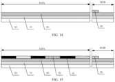
- FIG. 14 is a schematic diagram of a structure of a second substrate after a cut stop layer is formed according to an embodiment of the present disclosure.
- FIG. 15 is a schematic diagram of a structure of a second substrate after a black matrix and a color filter layer are formed according to an embodiment of the present disclosure.
- a display panel is mainly composed of a Thin Film Transistor (TFT) substrate, a second substrate, and a Liquid Crystal (LC) layer disposed between the two substrates.
- TFT Thin Film Transistor
- LC Liquid Crystal
- the second substrate needs to be cut to expose a bonding pad on the first substrate, and laser cutting is a commonly-used method. If the second substrate is cut before the first substrate and the second substrate are cell-assembled, due to a high energy density of a laser, large thermal stress will be generated at a cutting position, leading to a ridge at an edge of a cutting line, which in turn causes problems such as defective cell-assembly and uneven thickness of boxes between the first substrate and the second substrate.
- a Liquid crystal display has advantages of high image quality, small size, light weight, low voltage drive, low power consumption, wide application range, and etc., and is widely used in consumer electronics or computer products such as a TV, a mobile phone, and a computer monitor.
- a liquid crystal display panel is mainly composed of a Thin Film Transistor (TFT) substrate, a second substrate, and a Liquid Crystal (LC) layer disposed between the two substrates.
- TFT Thin Film Transistor
- LC Liquid Crystal
- the second substrate is cut before the first substrate and the second substrate are cell-assembled, due to a high energy density of a laser, a large thermal stress will be generated at a laser cutting position, leading to a ridge at an edge of a cutting line, which in turn causes problems such as defective cell-assembly and uneven thickness of boxes between the first substrate and the second substrate.
- a thermal stress generated at a laser cutting position will easily cause damage or failure to bonding pads and signal leads on the first substrate, thereby resulting in a problem of poor display or display failure of the display panel.
- An exemplary embodiment of the present disclosure provides a display panel including a first substrate, a second substrate, and a liquid crystal layer disposed between the first substrate and the second substrate, wherein the first substrate includes a first display region and a bonding region disposed on a side of the first display region; the second substrate includes a second display region and a cutting region disposed on a side of the second display region; an orthographic projection of the cutting region on the first substrate overlaps an orthographic projection of the bonding region on the first substrate; and the cutting region is provided with a cutting line.
- a side of the second substrate facing the first substrate is further provided with a cut stop layer, and an orthographic projection of the cut stop layer on the second substrate includes an orthographic projection of the cutting line on the second substrate.
- the cut stop layer is disposed on the side of the second substrate facing the first substrate, and the orthographic projection of the cut stop layer on the second substrate includes the orthographic projection of the cutting line on the second substrate, so that a laser energy will not cause damage or failure to bonding pad or signal leads on the first substrate, thereby improving display performance of the display panel.
- the cut stop layer may be disposed on a side of the first substrate facing the second substrate, which is not limited hereto in the present disclosure.
- FIG. 1 is a schematic diagram of a structure of a first substrate 100 according to an embodiment of the present disclosure
- FIG. 2 is a schematic diagram of a structure of a second substrate 101 according to an embodiment of the present disclosure
- FIG. 3 is a schematic sectional view in an AA direction after the first substrate 100 and the second substrate 101 respectively as shown in FIG. 1 and FIG. 2 being cell-assembled.
- the first substrate 100 includes a first display region 100 A, and a bonding region 100 B disposed on a side of the first display region 100 A.
- the bonding region 100 B includes a plurality of bonding pads 46 and a plurality of signal leads 47 ;
- the second substrate 101 includes a second display region 101 A and a cutting region 101 B disposed on a side of the second display region 101 A; positions of the first display region 100 A and the second display region 101 A correspond to each other; an orthographic projection of the cutting region 101 B on the first substrate 100 and an orthographic projection of the bonding region 100 B on the first substrate 100 overlap.
- the cutting region 101 B is provided with a cutting line 1011 .
- a side of the second substrate 101 facing the first substrate 100 or a side of the first substrate 100 facing the second substrate 101 includes a cut stop layer 90
- an orthographic projection of the cut stop layer 90 on the second substrate 101 includes an orthographic projection of the cutting line 1011 on the second substrate 101 .
- FIG. 3 only illustrates a relative positional relationship among the cutting region 101 B, a bonding pad 46 , and the cut stop layer 90 , and does not represent an actual film layer structure of the first substrate 100 and the second substrate 101 .
- an orthographic projection of the cut stop layer 90 on the second substrate 101 includes an orthographic projection of the cutting line 1011 on the second substrate 101 , which means that the orthographic projection of the cutting line 1011 on the second substrate 101 falls within a boundary line of the orthographic projection of the cut stop layer 90 on the second substrate 101 .
- a length of the cut stop layer 90 in a first direction is equal to a length of the second substrate 101 in the first direction.
- the cut stop layer 90 includes a first side 9001 and a second side 9002 which are oppositely disposed along a second direction y.
- a distance a between an orthographic projection of the first side 9001 on the second substrate 101 and an orthographic projection of the cutting line 1011 on the second substrate 101 is greater than or equal to a preset first distance.
- a distance a between an orthographic projection of the second side 9002 on the second substrate 101 and an orthographic projection of the cutting line 1011 on the second substrate 101 is greater than or equal to a preset first distance, the first direction x and the second direction y intersect.
- the first distance may be 30 microns to 2 millimeters.
- the first distance a may be 200 microns.
- the first direction x and the second direction y are perpendicular to each other.
- a distance between the first side 9001 and the second display region 101 A is smaller than a distance between the second side 9002 and the second display region 101 A.
- the first substrate 100 further includes a first sealant region 100 C, which is disposed around the first display region 100 A and located on a side of the bonding region 100 B facing the first display region 100 A; the second substrate 101 further includes a second sealant region 101 C, which is disposed around the second display region 101 A and located on a side of the cutting region 101 B facing the second display region 101 A.
- a sealant 93 is disposed between the first sealant region 100 C and the second sealant region 101 C, and a shortest distance b between the first side 9001 and the second sealant region 101 C is greater than a preset second distance.
- the second distance may be 25 microns to 35 microns.
- the second distance may be 30 microns.
- the cut stop layer 90 may be made of one or more metals such as platinum (Pt), ruthenium (Ru), gold (Au), silver (Ag), molybdenum (Mo), chromium (Cr), aluminum (Al), tantalum (Ta), titanium (Ti), and tungsten (W).
- metals such as platinum (Pt), ruthenium (Ru), gold (Au), silver (Ag), molybdenum (Mo), chromium (Cr), aluminum (Al), tantalum (Ta), titanium (Ti), and tungsten (W).
- a thickness of the cut stop layer 90 may be 500 to 5000 angstroms.
- a thickness of the cut stop layer 90 may be 1000 angstroms.
- a width of the cut stop layer 90 in the second direction y may be greater than 100 microns.
- a width of the cut stop layer 90 in the second direction y may be 300 microns.
- the second display region 101 A includes a second flexible base substrate layer, a second insulating layer disposed on the second flexible base substrate layer, a black matrix disposed on the second insulating layer, and a color filter layer disposed on the second insulating layer and located between adjacent black matrices.
- the cutting region 101 B includes a second flexible base substrate layer, a second insulating layer disposed on the second flexible base substrate layer, and a cut stop layer disposed on the second insulating layer.
- a “patterning process” mentioned in the exemplary embodiment includes procedures such as film layer deposition, photoresist coating, mask exposure, development, etching, and photoresist stripping, and is a mature preparation process in related art.
- Deposition may be performed by using a known process such as sputtering, evaporation, and chemical vapor deposition.
- Coating may be performed by using a known coating process, and etching may be performed by using a known approach, and a display apparatus is not limited here.
- a “thin film” refers to a layer of thin film manufactured through a certain material on a base substrate by using a deposition or coating process. If the “thin film” does not need a patterning process during a whole manufacturing process, the “thin film” may also be called a “layer”. If the “thin film” needs a patterning process during the whole manufacturing process, it is called a “thin film” before the patterning process and is called a “layer” after the patterning process. The “layer” subsequent to the patterning process contains at least one “pattern”.
- the preparation process of the display panel in the exemplary embodiment mainly includes following acts.
- the preparation of the first substrate 100 in the act (1) includes following contents.
- the first rigid substrate 10 may be a substrate made of a material with certain firmness such as glass, quartz, or transparent resin.
- the first flexible base substrate layer 20 may be a Polyimide (PI) layer.
- forming the first flexible base substrate layer 20 on the first rigid substrate 10 may include: coating a layer of PI solution on the first rigid substrate 10 , and drying the PI solution to remove solvent of the PI solution, so that solutes of the PI solution are remained to form the first flexible base substrate layer 20 .
- a drying process may be, for example, a low-pressure drying process, a high-pressure drying process, or an air-cooled drying process, which is not limited hereto in the embodiments of the present disclosure.
- the first insulating layer 30 is also called a first Buffer layer, which is used to improve water and oxygen resistance of a base substrate.
- Forming the pattern of the common electrode 40 includes: depositing a first transparent conductive thin film on the first insulating layer 30 of the first display region 100 A; coating a layer of photoresist on the first transparent conductive thin film; exposing and developing the photoresist by using a mask; forming an unexposed region at a position of the pattern of the common electrode; keeping the photoresist; forming a fully exposed region at other positions; removing the photoresist; etching the first transparent conductive thin film at the fully exposed region and stripping the remaining photoresist to form the pattern of the common electrode 40 .
- the common electrode may be a planar electrode.
- the bonding region 100 B which includes the first rigid substrate 10 , the first flexible base substrate layer 20 disposed on the first rigid substrate 10 , and the first insulating layer 30 disposed on the first flexible base substrate layer 20 .
- Forming the patterns of the gate line, the common electrode line, and the gate electrode 41 include: depositing a first metal thin film on the first insulating layer 30 of the first display region 100 A; coating a layer of photoresist on the first metal thin film; exposing and developing the photoresist by using a mask; forming an unexposed region at positions of the patterns of the gate line, the common electrode line, and the gate electrode 41 ; keeping the photoresist; forming a fully exposed region at other positions; removing the photoresist; etching the first metal thin film at the fully exposed region and stripping the remaining photoresist to form the patterns of the gate line, the common electrode line, and the gate electrode 41 .
- the gate line and the gate electrode 41 may have an integrated structure, and the gate electrode 41 is in charge of providing turn-on and turn-off voltages of a thin film transistor.
- the common electrode line is parallel to the gate line and directly connected to the common electrode 40 (the common electrode line is directly deposited on an upper edge of the common electrode), and is in charge of introducing a common voltage. In this patterning process, there is no change in a film layer structure of the bonding region 100 B.
- Forming the pattern of the active layer in the first display region 100 A includes: depositing a gate insulating layer 42 covering an entire base substrate, then depositing an active layer thin film, patterning the active layer thin film, and forming the pattern of the active layer 43 in the first display region 100 A, wherein the active layer 43 is above the gate electrode 41 .
- this patterning process only one gate insulating layer 42 is added on the first insulating layer 30 in the film layer structure of the bonding region 100 B.
- the process includes: depositing a second metal thin film, patterning the second metal thin film to form the patterns of the data line, the source electrode 44 , and the drain electrode 45 , and the patterns of the bonding pads 46 and the signal leads 47 , wherein the source electrode 44 is connected to the data line, and the drain electrode 45 and the source electrode 44 are oppositely disposed to form a horizontal channel.
- the gate electrode 41 , the active layer 43 , the source electrode 44 , and the drain electrode 45 constitute a thin film transistor, and the data line perpendicularly intersects with the gate line and is in charge of providing a signal voltage.
- Forming the pattern of the passivation layer 48 with via holes includes: depositing a passivation layer thin film, coating a layer of photoresist on the passivation layer thin film, exposing and developing the photoresist by a mask, forming a fully exposed region at a position of a first via hole, removing the photoresist, forming unexposed regions at other positions, keeping the photoresist, etching the passivation layer thin film in the fully exposed region and stripping the remaining photoresist to form the pattern of the passivation layer 48 with the first via hole 48 a and a second via hole 48 b , wherein the first via hole 48 a is located at a position of the drain electrode 45 , and the passivation layer thin film in the first via hole 48 a is etched away to expose a surface of the drain electrode 45 ; the second via hole
- Forming the pattern of the pixel electrode 50 includes: depositing a second transparent conductive thin film, patterning the second transparent conductive thin film to form the pattern of the pixel electrode 50 , wherein the pixel electrode 50 is located in a pixel region defined by a gate line and a data line, and is connected to the drain electrode 45 through the first via 48 a .
- the pixel electrode 50 is a slit electrode with a certain inclination angle. In this patterning process, there is no change in a film layer structure of the bonding region 100 B.
- the first metal thin film and the second metal thin film may be made of one or more metals, such as platinum (Pt), ruthenium (Ru), gold (Au), silver (Ag), molybdenum (Mo), chromium (Cr), aluminum (Al), tantalum (Ta), titanium (Ti), and tungsten (W).
- the first insulating thin film, the gate insulating layer, and the passivation layer may be made of silicon nitride (SiNx), silicon oxide (SiOx), or a SiNx/SiOx composite thin film.
- the first transparent conductive thin film and the second transparent conductive thin film may be made of indium tin oxide (ITO) or indium zinc oxide (IZO).
- the material of the active layer may be silicon semiconductor or metal oxide semiconductor.
- the first substrate 100 of this exemplary embodiment may be prepared through five patterning processes or fewer patterning processes.
- the above-mentioned patterning process for forming the pattern of the common electrode and the patterning process for forming the patterns of the gate line, the common electrode line, and the gate electrode may be formed by an one-time patterning process using a halftone mask or gray tone mask technology
- the patterning process for forming the pattern of the active layer and the patterning process for forming the patterns of the data line, the source electrode, and the drain electrode may also be formed by an one-time patterning process using a halftone mask or gray tone mask technology.
- this exemplary embodiment describes a structure of a thin film transistor by taking a bottom gate structure as an example, the thin film transistor may also adopt a top gate structure in an actual implementation, which is not limited hereto in the present disclosure.
- ADS type first substrate is taken as an example in this exemplary embodiment, a technical concept of the present disclosure may also be applied to Twisted Nematic (TN) type, In Plane switching (IPS) type, and Fringe Field Switching (FFS) type first substrates.
- TN Twisted Nematic
- IPS In Plane switching
- FFS Fringe Field Switching
- the preparation of the second substrate 101 in the act (1) may include following contents.
- the second rigid substrate 60 may be a substrate made of a material with certain firmness such as glass, quartz, or transparent resin.
- the second flexible base substrate layer 70 may be a Polyimide (PI) layer.
- forming the second flexible base substrate layer 70 on the second rigid substrate 60 may include: coating a layer of PI solution on the second rigid substrate 60 , and drying the PI solution to remove solvent of the PI solution, so that solutes of the PI solution remain to form the second flexible base substrate layer 70 .
- a drying process may be, for example, a low-pressure drying process, a high-pressure drying process, or an air-cooled drying process, which is not limited hereto in the embodiments of the present disclosure.
- the second insulating layer 80 is also called a second Buffer layer, which is used to improve water and oxygen resistance of a base substrate.
- the first insulating film may be made of silicon nitride (SiNx), silicon oxide (SiOx), or a SiNx/SiOx composite thin film.
- Forming the cut stop layer 90 includes: depositing a third metal thin film and patterning the third metal thin film to form a pattern of the cut stop layer 90 .
- an orthographic projection of the cut stop layer 90 on the second substrate 101 covers an orthographic projection of the cutting line 1011 on the second substrate 101 .
- the cutting line 1011 in the exemplary embodiment of the present disclosure may be a virtual straight line, which may be identified by an alignment mark and used for alignment during laser cutting.
- a width of the cut stop layer 90 in the second direction y is greater than 100 microns, and preferably, a width of the cut stop layer 90 in the second direction y may be 300 microns.
- a thickness of the cut stop layer 90 may be 500 to 5000 angstroms, and preferably, a thickness of the cut stop layer 90 may be 1000 angstroms.
- the cut stop layer 90 may be made of one or more metals, such as platinum (Pt), ruthenium (Ru), gold (Au), silver (Ag), molybdenum (Mo), chromium (Cr), aluminum (Al), tantalum (Ta), titanium (Ti), and tungsten (W).
- metals such as platinum (Pt), ruthenium (Ru), gold (Au), silver (Ag), molybdenum (Mo), chromium (Cr), aluminum (Al), tantalum (Ta), titanium (Ti), and tungsten (W).
- an order of forming patterns of the black matrices and the color filter layers and forming the cut stop layer 90 may be reversed, that is, the pattern of the cut stop layer 90 may be formed first, and then the patterns of the black matrices and color filter layers are formed.
- the act (2) may include: coating a sealant 93 on a periphery of the first substrate 100 , dropping liquid crystal on the second substrate 101 , and cell-assembling the second substrate 101 filled with liquid crystal with the first substrate 100 coated with the sealant 93 ; and solidifying the sealant 93 by ultraviolet rays to complete an cell-assembly process.
- the act (3) may include: performing single-side cutting on the second substrate 101 by using a laser incident from a side of the second rigid substrate 60 along a cutting region. A residual energy of the laser penetrating after cutting the second substrate 101 will be absorbed or reflected by the cut stop layer, and will not cause damage to the first substrate. After the cutting is completed, the cutting region 101 B is cut off, and there will be residual metal of the cut stop layer in the cutting region. However, due to protection of an insulating layer on the bonding region, the residual metal of the cut stop layer will not cause a risk of a short circuit.
- a transmittance of a laser wavelength used for laser cutting to a rigid carrier is greater than 80%, and preferably, a transmittance to the rigid carrier is greater than 90%.
- a transmittance of a laser wavelength used for laser cutting to a flexible substrate is less than 5%; preferably, a transmittance to the flexible substrate is less than 1%.
- a transmittance of a laser wavelength used for laser cutting to the cut stop layer 90 is less than 1%; preferably, a transmittance to the cut stop layer 90 is less than 0.01%.
- the act (4) may include: lifting off the second rigid substrate 60 and the second flexible base substrate layer 70 and lifting off the first rigid substrate 10 and the second flexible base substrate layer 20 by using a lift-off process or a laser.
- the act (5) may include: attaching a first polarizer on a side of the first substrate 100 away from the second substrate 101 and attaching a second polarizer on a side of the second substrate 101 away from the first substrate 100 .
- the act (6) may include: bonding a chip and a flexible circuit board for the first substrate 100 .
- the cut stop layer 90 is disposed on a side of the second substrate 101 facing the first substrate 100 , and an orthographic projection of the cut stop layer 90 on the second substrate 101 includes an orthographic projection of the cutting line 1011 on the second substrate 101 , so that a laser energy will not cause damage or failure to the bonding pads 46 or signal leads 47 on the first substrate 100 , thereby improving display performance of the display panel.
- An exemplary embodiment of the present disclosure further provides a display apparatus, including the aforementioned display panel.
- the display apparatus may be: any product or component with a display function, such as a mobile phone, a tablet computer, a television, a display, a laptop computer, a digital photo frame, or a navigator.
- an orientation or positional relation indicated by terms “middle”, “up”, “down”, “front”, “back”, “vertical”, “horizontal”, “top”, “bottom”, “inside”, “outside”, and etc. is based on an orientation or positional relation shown in the drawings, and is merely for convenience of describing the present disclosure and simplifying the description, rather than indicating or implying that the apparatus or elements referred to must have a particular orientation, or configured or operated in a particular orientation. Thus, it may not be construed as limitations on the present disclosure.
Landscapes
- Physics & Mathematics (AREA)
- Nonlinear Science (AREA)
- Mathematical Physics (AREA)
- Chemical & Material Sciences (AREA)
- Crystallography & Structural Chemistry (AREA)
- General Physics & Mathematics (AREA)
- Optics & Photonics (AREA)
- Devices For Indicating Variable Information By Combining Individual Elements (AREA)
Abstract
Description
Claims (12)
Applications Claiming Priority (2)
| Application Number | Priority Date | Filing Date | Title |
|---|---|---|---|
| CN202022141857.9U CN212694214U (en) | 2020-09-25 | 2020-09-25 | Display panel and display device |
| CN202022141857.9 | 2020-09-25 |
Publications (2)
| Publication Number | Publication Date |
|---|---|
| US20220100012A1 US20220100012A1 (en) | 2022-03-31 |
| US11662614B2 true US11662614B2 (en) | 2023-05-30 |
Family
ID=74885803
Family Applications (1)
| Application Number | Title | Priority Date | Filing Date |
|---|---|---|---|
| US17/406,109 Active US11662614B2 (en) | 2020-09-25 | 2021-08-19 | Display panel and display apparatus |
Country Status (2)
| Country | Link |
|---|---|
| US (1) | US11662614B2 (en) |
| CN (1) | CN212694214U (en) |
Families Citing this family (1)
| Publication number | Priority date | Publication date | Assignee | Title |
|---|---|---|---|---|
| CN113539127B (en) * | 2021-07-09 | 2023-04-11 | 京东方科技集团股份有限公司 | Display substrate, preparation method thereof and display device |
Citations (3)
| Publication number | Priority date | Publication date | Assignee | Title |
|---|---|---|---|---|
| KR20060073757A (en) * | 2004-12-24 | 2006-06-29 | 삼성전자주식회사 | Scribing stage and liquid crystal display manufactured using the same |
| US20120099056A1 (en) * | 2010-10-26 | 2012-04-26 | Samsung Electronics Co., Ltd. | Display panel, display apparatus having the same, method of manufacturing the same and method of cutting the same |
| US20220085306A1 (en) * | 2020-09-17 | 2022-03-17 | Innolux Corporation | Electronic device |
-
2020
- 2020-09-25 CN CN202022141857.9U patent/CN212694214U/en active Active
-
2021
- 2021-08-19 US US17/406,109 patent/US11662614B2/en active Active
Patent Citations (3)
| Publication number | Priority date | Publication date | Assignee | Title |
|---|---|---|---|---|
| KR20060073757A (en) * | 2004-12-24 | 2006-06-29 | 삼성전자주식회사 | Scribing stage and liquid crystal display manufactured using the same |
| US20120099056A1 (en) * | 2010-10-26 | 2012-04-26 | Samsung Electronics Co., Ltd. | Display panel, display apparatus having the same, method of manufacturing the same and method of cutting the same |
| US20220085306A1 (en) * | 2020-09-17 | 2022-03-17 | Innolux Corporation | Electronic device |
Also Published As
| Publication number | Publication date |
|---|---|
| US20220100012A1 (en) | 2022-03-31 |
| CN212694214U (en) | 2021-03-12 |
Similar Documents
| Publication | Publication Date | Title |
|---|---|---|
| US7050131B2 (en) | Liquid crystal display device having black seal pattern and external resin pattern, and method of fabricating the same | |
| KR101283366B1 (en) | An Electrophoretic display device and method of fabricating the same | |
| KR101905757B1 (en) | Array substrate for fringe field switching mode liquid crystal display device and method for fabricating the same | |
| KR100857133B1 (en) | Array substrate for liquid crystal display device and manufacturing method thereof | |
| US9244320B2 (en) | Liquid crystal display and manufacturing method thereof | |
| CN103474432B (en) | A kind of array base palte and preparation method thereof and display unit | |
| US12105383B2 (en) | Array substrate having conductive bumps, liquid crystal display panel and method for manufacturing the same, and display apparatus | |
| JP4235576B2 (en) | Color filter substrate and display device using the same | |
| KR101870986B1 (en) | Method for fabricating thin film transistor array substrate | |
| KR100710532B1 (en) | Liquid crystal display and fabricating the same | |
| CN104360557A (en) | Array substrate, manufacturing method thereof and display device | |
| JP5107596B2 (en) | Liquid crystal display device and manufacturing method thereof | |
| KR102503756B1 (en) | Display device and manufacturing method thereof | |
| JP2004252047A (en) | Transflective display | |
| JP4875702B2 (en) | Transflective liquid crystal display device and manufacturing method thereof | |
| KR20110040222A (en) | Fringe field type liquid crystal display device and manufacturing method thereof | |
| US11662614B2 (en) | Display panel and display apparatus | |
| KR20040050237A (en) | Array substrate for LCD and Method for fabricating of the same | |
| KR20130030975A (en) | Liquid crystal display device | |
| KR20070070806A (en) | Thin film transistor substrate and its manufacturing method | |
| CN101140939A (en) | Display panel and manufacturing method thereof | |
| KR20170054597A (en) | Display substrate, liquid crystal display comprising the same, and manufacturing method the same | |
| WO2010097855A1 (en) | Method for manufacturing display panel | |
| KR20020089005A (en) | A substrate for Transflective LCD and a method of fabricating thereof | |
| JP2005215277A (en) | Liquid crystal display device and manufacturing method thereof |
Legal Events
| Date | Code | Title | Description |
|---|---|---|---|
| FEPP | Fee payment procedure |
Free format text: ENTITY STATUS SET TO UNDISCOUNTED (ORIGINAL EVENT CODE: BIG.); ENTITY STATUS OF PATENT OWNER: LARGE ENTITY |
|
| AS | Assignment |
Owner name: BOE TECHNOLOGY GROUP CO., LTD., CHINA Free format text: ASSIGNMENT OF ASSIGNORS INTEREST;ASSIGNOR:HSIEH, CHANGHAN;REEL/FRAME:057391/0569 Effective date: 20210802 |
|
| STPP | Information on status: patent application and granting procedure in general |
Free format text: DOCKETED NEW CASE - READY FOR EXAMINATION |
|
| STPP | Information on status: patent application and granting procedure in general |
Free format text: NON FINAL ACTION MAILED |
|
| STPP | Information on status: patent application and granting procedure in general |
Free format text: RESPONSE TO NON-FINAL OFFICE ACTION ENTERED AND FORWARDED TO EXAMINER |
|
| STPP | Information on status: patent application and granting procedure in general |
Free format text: FINAL REJECTION MAILED |
|
| STPP | Information on status: patent application and granting procedure in general |
Free format text: DOCKETED NEW CASE - READY FOR EXAMINATION |
|
| STCF | Information on status: patent grant |
Free format text: PATENTED CASE |