US11600968B2 - Single-mode micro-laser based on single whispering gallery mode optical microcavity and preparation method thereof - Google Patents
Single-mode micro-laser based on single whispering gallery mode optical microcavity and preparation method thereof Download PDFInfo
- Publication number
- US11600968B2 US11600968B2 US17/397,992 US202117397992A US11600968B2 US 11600968 B2 US11600968 B2 US 11600968B2 US 202117397992 A US202117397992 A US 202117397992A US 11600968 B2 US11600968 B2 US 11600968B2
- Authority
- US
- United States
- Prior art keywords
- mode
- optical
- optical microcavity
- microcavity
- optical fiber
- Prior art date
- Legal status (The legal status is an assumption and is not a legal conclusion. Google has not performed a legal analysis and makes no representation as to the accuracy of the status listed.)
- Active, expires
Links
Images


Classifications
-
- H—ELECTRICITY
- H01—ELECTRIC ELEMENTS
- H01S—DEVICES USING THE PROCESS OF LIGHT AMPLIFICATION BY STIMULATED EMISSION OF RADIATION [LASER] TO AMPLIFY OR GENERATE LIGHT; DEVICES USING STIMULATED EMISSION OF ELECTROMAGNETIC RADIATION IN WAVE RANGES OTHER THAN OPTICAL
- H01S5/00—Semiconductor lasers
- H01S5/10—Construction or shape of the optical resonator, e.g. extended or external cavity, coupled cavities, bent-guide, varying width, thickness or composition of the active region
- H01S5/1042—Optical microcavities, e.g. cavity dimensions comparable to the wavelength
-
- H—ELECTRICITY
- H01—ELECTRIC ELEMENTS
- H01S—DEVICES USING THE PROCESS OF LIGHT AMPLIFICATION BY STIMULATED EMISSION OF RADIATION [LASER] TO AMPLIFY OR GENERATE LIGHT; DEVICES USING STIMULATED EMISSION OF ELECTROMAGNETIC RADIATION IN WAVE RANGES OTHER THAN OPTICAL
- H01S5/00—Semiconductor lasers
- H01S5/10—Construction or shape of the optical resonator, e.g. extended or external cavity, coupled cavities, bent-guide, varying width, thickness or composition of the active region
- H01S5/1071—Ring-lasers
- H01S5/1075—Disk lasers with special modes, e.g. whispering gallery lasers
-
- H—ELECTRICITY
- H01—ELECTRIC ELEMENTS
- H01S—DEVICES USING THE PROCESS OF LIGHT AMPLIFICATION BY STIMULATED EMISSION OF RADIATION [LASER] TO AMPLIFY OR GENERATE LIGHT; DEVICES USING STIMULATED EMISSION OF ELECTROMAGNETIC RADIATION IN WAVE RANGES OTHER THAN OPTICAL
- H01S3/00—Lasers, i.e. devices using stimulated emission of electromagnetic radiation in the infrared, visible or ultraviolet wave range
- H01S3/05—Construction or shape of optical resonators; Accommodation of active medium therein; Shape of active medium
- H01S3/06—Construction or shape of active medium
- H01S3/063—Waveguide lasers, i.e. whereby the dimensions of the waveguide are of the order of the light wavelength
- H01S3/0632—Thin film lasers in which light propagates in the plane of the thin film
- H01S3/0637—Integrated lateral waveguide, e.g. the active waveguide is integrated on a substrate made by Si on insulator technology (Si/SiO2)
-
- H—ELECTRICITY
- H01—ELECTRIC ELEMENTS
- H01S—DEVICES USING THE PROCESS OF LIGHT AMPLIFICATION BY STIMULATED EMISSION OF RADIATION [LASER] TO AMPLIFY OR GENERATE LIGHT; DEVICES USING STIMULATED EMISSION OF ELECTROMAGNETIC RADIATION IN WAVE RANGES OTHER THAN OPTICAL
- H01S5/00—Semiconductor lasers
- H01S5/02—Structural details or components not essential to laser action
- H01S5/022—Mountings; Housings
- H01S5/0225—Out-coupling of light
- H01S5/02251—Out-coupling of light using optical fibres
-
- H—ELECTRICITY
- H01—ELECTRIC ELEMENTS
- H01S—DEVICES USING THE PROCESS OF LIGHT AMPLIFICATION BY STIMULATED EMISSION OF RADIATION [LASER] TO AMPLIFY OR GENERATE LIGHT; DEVICES USING STIMULATED EMISSION OF ELECTROMAGNETIC RADIATION IN WAVE RANGES OTHER THAN OPTICAL
- H01S5/00—Semiconductor lasers
- H01S5/02—Structural details or components not essential to laser action
- H01S5/026—Monolithically integrated components, e.g. waveguides, monitoring photo-detectors, drivers
-
- H—ELECTRICITY
- H01—ELECTRIC ELEMENTS
- H01S—DEVICES USING THE PROCESS OF LIGHT AMPLIFICATION BY STIMULATED EMISSION OF RADIATION [LASER] TO AMPLIFY OR GENERATE LIGHT; DEVICES USING STIMULATED EMISSION OF ELECTROMAGNETIC RADIATION IN WAVE RANGES OTHER THAN OPTICAL
- H01S5/00—Semiconductor lasers
- H01S5/06—Arrangements for controlling the laser output parameters, e.g. by operating on the active medium
- H01S5/065—Mode locking; Mode suppression; Mode selection ; Self pulsating
- H01S5/0651—Mode control
- H01S5/0653—Mode suppression, e.g. specific multimode
- H01S5/0654—Single longitudinal mode emission
-
- H—ELECTRICITY
- H01—ELECTRIC ELEMENTS
- H01S—DEVICES USING THE PROCESS OF LIGHT AMPLIFICATION BY STIMULATED EMISSION OF RADIATION [LASER] TO AMPLIFY OR GENERATE LIGHT; DEVICES USING STIMULATED EMISSION OF ELECTROMAGNETIC RADIATION IN WAVE RANGES OTHER THAN OPTICAL
- H01S5/00—Semiconductor lasers
- H01S5/10—Construction or shape of the optical resonator, e.g. extended or external cavity, coupled cavities, bent-guide, varying width, thickness or composition of the active region
- H01S5/1003—Waveguide having a modified shape along the axis, e.g. branched, curved, tapered, voids
- H01S5/1014—Tapered waveguide, e.g. spotsize converter
-
- H—ELECTRICITY
- H01—ELECTRIC ELEMENTS
- H01S—DEVICES USING THE PROCESS OF LIGHT AMPLIFICATION BY STIMULATED EMISSION OF RADIATION [LASER] TO AMPLIFY OR GENERATE LIGHT; DEVICES USING STIMULATED EMISSION OF ELECTROMAGNETIC RADIATION IN WAVE RANGES OTHER THAN OPTICAL
- H01S5/00—Semiconductor lasers
- H01S5/10—Construction or shape of the optical resonator, e.g. extended or external cavity, coupled cavities, bent-guide, varying width, thickness or composition of the active region
- H01S5/1028—Coupling to elements in the cavity, e.g. coupling to waveguides adjacent the active region, e.g. forward coupled [DFC] structures
-
- B—PERFORMING OPERATIONS; TRANSPORTING
- B82—NANOTECHNOLOGY
- B82Y—SPECIFIC USES OR APPLICATIONS OF NANOSTRUCTURES; MEASUREMENT OR ANALYSIS OF NANOSTRUCTURES; MANUFACTURE OR TREATMENT OF NANOSTRUCTURES
- B82Y20/00—Nanooptics, e.g. quantum optics or photonic crystals
-
- G—PHYSICS
- G02—OPTICS
- G02B—OPTICAL ELEMENTS, SYSTEMS OR APPARATUS
- G02B6/00—Light guides; Structural details of arrangements comprising light guides and other optical elements, e.g. couplings
- G02B6/24—Coupling light guides
- G02B6/25—Preparing the ends of light guides for coupling, e.g. cutting
-
- H—ELECTRICITY
- H01—ELECTRIC ELEMENTS
- H01S—DEVICES USING THE PROCESS OF LIGHT AMPLIFICATION BY STIMULATED EMISSION OF RADIATION [LASER] TO AMPLIFY OR GENERATE LIGHT; DEVICES USING STIMULATED EMISSION OF ELECTROMAGNETIC RADIATION IN WAVE RANGES OTHER THAN OPTICAL
- H01S2301/00—Functional characteristics
- H01S2301/16—Semiconductor lasers with special structural design to influence the modes, e.g. specific multimode
- H01S2301/163—Single longitudinal mode
-
- H—ELECTRICITY
- H01—ELECTRIC ELEMENTS
- H01S—DEVICES USING THE PROCESS OF LIGHT AMPLIFICATION BY STIMULATED EMISSION OF RADIATION [LASER] TO AMPLIFY OR GENERATE LIGHT; DEVICES USING STIMULATED EMISSION OF ELECTROMAGNETIC RADIATION IN WAVE RANGES OTHER THAN OPTICAL
- H01S3/00—Lasers, i.e. devices using stimulated emission of electromagnetic radiation in the infrared, visible or ultraviolet wave range
- H01S3/10—Controlling the intensity, frequency, phase, polarisation or direction of the emitted radiation, e.g. switching, gating, modulating or demodulating
- H01S3/102—Controlling the intensity, frequency, phase, polarisation or direction of the emitted radiation, e.g. switching, gating, modulating or demodulating by controlling the active medium, e.g. by controlling the processes or apparatus for excitation
- H01S3/1022—Controlling the intensity, frequency, phase, polarisation or direction of the emitted radiation, e.g. switching, gating, modulating or demodulating by controlling the active medium, e.g. by controlling the processes or apparatus for excitation by controlling the optical pumping
-
- H—ELECTRICITY
- H01—ELECTRIC ELEMENTS
- H01S—DEVICES USING THE PROCESS OF LIGHT AMPLIFICATION BY STIMULATED EMISSION OF RADIATION [LASER] TO AMPLIFY OR GENERATE LIGHT; DEVICES USING STIMULATED EMISSION OF ELECTROMAGNETIC RADIATION IN WAVE RANGES OTHER THAN OPTICAL
- H01S3/00—Lasers, i.e. devices using stimulated emission of electromagnetic radiation in the infrared, visible or ultraviolet wave range
- H01S3/14—Lasers, i.e. devices using stimulated emission of electromagnetic radiation in the infrared, visible or ultraviolet wave range characterised by the material used as the active medium
- H01S3/16—Solid materials
- H01S3/1601—Solid materials characterised by an active (lasing) ion
- H01S3/1603—Solid materials characterised by an active (lasing) ion rare earth
- H01S3/1608—Solid materials characterised by an active (lasing) ion rare earth erbium
-
- H—ELECTRICITY
- H01—ELECTRIC ELEMENTS
- H01S—DEVICES USING THE PROCESS OF LIGHT AMPLIFICATION BY STIMULATED EMISSION OF RADIATION [LASER] TO AMPLIFY OR GENERATE LIGHT; DEVICES USING STIMULATED EMISSION OF ELECTROMAGNETIC RADIATION IN WAVE RANGES OTHER THAN OPTICAL
- H01S3/00—Lasers, i.e. devices using stimulated emission of electromagnetic radiation in the infrared, visible or ultraviolet wave range
- H01S3/14—Lasers, i.e. devices using stimulated emission of electromagnetic radiation in the infrared, visible or ultraviolet wave range characterised by the material used as the active medium
- H01S3/16—Solid materials
- H01S3/1628—Solid materials characterised by a semiconducting matrix
-
- H—ELECTRICITY
- H01—ELECTRIC ELEMENTS
- H01S—DEVICES USING THE PROCESS OF LIGHT AMPLIFICATION BY STIMULATED EMISSION OF RADIATION [LASER] TO AMPLIFY OR GENERATE LIGHT; DEVICES USING STIMULATED EMISSION OF ELECTROMAGNETIC RADIATION IN WAVE RANGES OTHER THAN OPTICAL
- H01S3/00—Lasers, i.e. devices using stimulated emission of electromagnetic radiation in the infrared, visible or ultraviolet wave range
- H01S3/14—Lasers, i.e. devices using stimulated emission of electromagnetic radiation in the infrared, visible or ultraviolet wave range characterised by the material used as the active medium
- H01S3/16—Solid materials
- H01S3/169—Nanoparticles, e.g. doped nanoparticles acting as a gain material
-
- H—ELECTRICITY
- H01—ELECTRIC ELEMENTS
- H01S—DEVICES USING THE PROCESS OF LIGHT AMPLIFICATION BY STIMULATED EMISSION OF RADIATION [LASER] TO AMPLIFY OR GENERATE LIGHT; DEVICES USING STIMULATED EMISSION OF ELECTROMAGNETIC RADIATION IN WAVE RANGES OTHER THAN OPTICAL
- H01S5/00—Semiconductor lasers
- H01S5/04—Processes or apparatus for excitation, e.g. pumping, e.g. by electron beams
- H01S5/041—Optical pumping
-
- H—ELECTRICITY
- H01—ELECTRIC ELEMENTS
- H01S—DEVICES USING THE PROCESS OF LIGHT AMPLIFICATION BY STIMULATED EMISSION OF RADIATION [LASER] TO AMPLIFY OR GENERATE LIGHT; DEVICES USING STIMULATED EMISSION OF ELECTROMAGNETIC RADIATION IN WAVE RANGES OTHER THAN OPTICAL
- H01S5/00—Semiconductor lasers
- H01S5/10—Construction or shape of the optical resonator, e.g. extended or external cavity, coupled cavities, bent-guide, varying width, thickness or composition of the active region
- H01S5/1028—Coupling to elements in the cavity, e.g. coupling to waveguides adjacent the active region, e.g. forward coupled [DFC] structures
- H01S5/1032—Coupling to elements comprising an optical axis that is not aligned with the optical axis of the active region
-
- H—ELECTRICITY
- H01—ELECTRIC ELEMENTS
- H01S—DEVICES USING THE PROCESS OF LIGHT AMPLIFICATION BY STIMULATED EMISSION OF RADIATION [LASER] TO AMPLIFY OR GENERATE LIGHT; DEVICES USING STIMULATED EMISSION OF ELECTROMAGNETIC RADIATION IN WAVE RANGES OTHER THAN OPTICAL
- H01S5/00—Semiconductor lasers
- H01S5/20—Structure or shape of the semiconductor body to guide the optical wave ; Confining structures perpendicular to the optical axis, e.g. index or gain guiding, stripe geometry, broad area lasers, gain tailoring, transverse or lateral reflectors, special cladding structures, MQW barrier reflection layers
- H01S5/22—Structure or shape of the semiconductor body to guide the optical wave ; Confining structures perpendicular to the optical axis, e.g. index or gain guiding, stripe geometry, broad area lasers, gain tailoring, transverse or lateral reflectors, special cladding structures, MQW barrier reflection layers having a ridge or stripe structure
- H01S5/2205—Structure or shape of the semiconductor body to guide the optical wave ; Confining structures perpendicular to the optical axis, e.g. index or gain guiding, stripe geometry, broad area lasers, gain tailoring, transverse or lateral reflectors, special cladding structures, MQW barrier reflection layers having a ridge or stripe structure comprising special burying or current confinement layers
- H01S5/2206—Structure or shape of the semiconductor body to guide the optical wave ; Confining structures perpendicular to the optical axis, e.g. index or gain guiding, stripe geometry, broad area lasers, gain tailoring, transverse or lateral reflectors, special cladding structures, MQW barrier reflection layers having a ridge or stripe structure comprising special burying or current confinement layers based on III-V materials
-
- H—ELECTRICITY
- H01—ELECTRIC ELEMENTS
- H01S—DEVICES USING THE PROCESS OF LIGHT AMPLIFICATION BY STIMULATED EMISSION OF RADIATION [LASER] TO AMPLIFY OR GENERATE LIGHT; DEVICES USING STIMULATED EMISSION OF ELECTROMAGNETIC RADIATION IN WAVE RANGES OTHER THAN OPTICAL
- H01S5/00—Semiconductor lasers
- H01S5/30—Structure or shape of the active region; Materials used for the active region
- H01S5/34—Structure or shape of the active region; Materials used for the active region comprising quantum well or superlattice structures, e.g. single quantum well [SQW] lasers, multiple quantum well [MQW] lasers or graded index separate confinement heterostructure [GRINSCH] lasers
- H01S5/341—Structures having reduced dimensionality, e.g. quantum wires
- H01S5/3412—Structures having reduced dimensionality, e.g. quantum wires quantum box or quantum dash
Definitions
- the present invention relates to preparation of a single-mode micro-lasers, and more particularly to a single-mode narrow-linewidth laser based on a single whispering gallery mode optical microcavity and a preparation method thereof, wherein dry etching is applied to film materials such as crystal, silicon dioxide, silicon, compound semiconductor materials and silicon nitride doped with a certain concentration of rare earth ions or organic macromolecules or containing quantum dots, and chemical polishing technology is also adopted, so as to obtain an active optical microcavity with a low loss and a high Q value.
- the single-mode micro-laser with a narrow line width and a low threshold can be obtained.
- Integrated optical path is designed to miniaturize and integrate optical devices and optical paths on a substrate, so as to reduce the size, energy consumption, and time delay of the optical system, as well as improve performance of the optical system such as stability and processing speed. It is expected to break through the energy consumption and bandwidth bottlenecks faced by conventional optical information processing systems.
- Micro-lasers especially single-mode micro-lasers with narrow linewidths, are one of the most important optical devices for constructing integrated optical paths, which have important applications in laser communication, precision measurement, and biosensing (L. He, et al., Nature Nanotechnol. Vol. 6, P 428-432, 2011).
- micro-lasers are usually prepared based on photonic crystal microcavities, Fabry-Perot microcavities and whispering gallery mode optical microcavities.
- the whispering gallery mode optical microcavity can realize confinement of the photons through continuous total internal reflection of light at the interface between the cavity material and the surrounding material with lower refractive index, which has a high quality factor and a small mode volume (DK Armani, et al., Nature Vol. 421, P 925-928, 2003). Therefore, the micro-laser based on the whispering gallery mode optical microcavity has the advantages of low threshold and narrow line width.
- optical microcavity For single-mode lasing, the size of the whispering gallery mode optical microcavity (hereinafter referred to as optical microcavity) is usually required to be in the sub-micron order to suppress the mode numbers, which inevitably increases the bending radiation loss of the microcavity, reduces the quality factor of the microcavity, and significantly increases the pump threshold and laser linewidth of the micro-laser.
- a commonly used effective method is to take advantage of the vernier effect of two coupled optical microcavities, so as to excite only the whispering gallery mode shared by the two microcavities, thereby obtaining single-mode lasing with low threshold and narrow linewidth (G. Griffel, IEEE Photon. Technol. Lett. Vol 12, P 1642-1644, 2000; L. Shang, et al., Opt. Lett. Vol. 33, P 1150-1152, 2008).
- the preparation process is complicated and such method is unsuitable for cost-effective preparation.
- Preparing a single-mode micro-laser with low threshold and narrow linewidth based on single optical microcavity has become an urgent need to improve the application level of optoelectronic integration technology.
- An object of the present invention is to provide to overcome challenges of conventional on-chip single-mode micro-laser preparation and provide a single-mode micro-laser based on a single whispering gallery mode optical microcavity.
- the single-mode micro-laser has a simple preparation process, a low threshold and a narrow line width.
- the present invention provides:
- a preparation method of a single-mode micro-laser based on a single whispering gallery mode optical microcavity comprising steps of:
- optical microcavity containing a gain material by dry etching, wherein the optical microcavity is the whispering gallery mode optical microcavity; a free spectral range of the optical microcavity is at least 1 ⁇ 2 of a spectral width of the gain material; the gain material is rare earth ions, quantum dots, or organic macromolecular luminescent materials; a cavity material of the optical microcavity is crystals, silicon dioxides, silicon, III-V compound semiconductor materials or silicon nitride films;
- the pump threshold is determined by a Q factor and a mode volume of the optical microcavity and a gain coefficient of the gain material, which comprises specific steps of: attaching the waist of the optical fiber cone to an edge of the optical microcavity, and inputting the pump light into one end of the optical fiber cone; restricting a wavelength of the pump light within an absorption spectrum wide range of the gain material;
- the optical microcavity displays a coherently combined composite mode with a polygonal configuration within an absorption range of the gain material, wherein the coherently combined mode is formed by superposition of a fundamental longitudinal spatial mode and a high-order longitudinal spatial modes, and is identical to the polygonal configuration in the step 4, wherein at this time, the pump light resonates with the coherently combined mode within the absorption spectrum of the gain material, and a lasing light resonates with a coherently combined mode within a fluorescence spectrum of the gain material;
- a preparation method of a single-mode micro-laser based on a single whispering gallery mode optical microcavity comprising steps of:
- optical microcavity containing a gain material by dry etching, wherein the optical microcavity is the whispering gallery mode optical microcavity; a free spectral range of the optical microcavity is at least 1 ⁇ 2 of a spectral width of the gain material; the gain material is rare earth ions, quantum dots, or organic macromolecular luminescent materials; a cavity material of the optical microcavity is crystals, silicon dioxides, silicon, III-V compound semiconductor materials or silicon nitride films;
- the pump threshold is determined by a Q factor and a mode volume of the optical microcavity and a gain coefficient of the gain material, which comprises specific steps of: attaching the optical waveguide to an edge of the optical microcavity, and inputting the pump light into one end of the optical waveguide; restricting a wavelength of the pump light within the absorption spectrum wide range of the gain material; continuously increasing the pump power of the pump light, wherein when the pump power of the pump light is greater than the pump threshold, the output power of the micro-laser from the optical waveguide increases linearly with the pump power; obtaining the pump threshold at an inflection point on a calculated growth curve;
- the single-mode micro-laser based on the single whispering gallery mode optical microcavity prepared by the above preparation methods comprises the single whispering gallery mode optical microcavity containing an active material, and the optical fiber cone or the optical waveguide, wherein the active material is rare earth ions, quantum dots, or organic macromolecular luminescent materials; the cavity material of the optical microcavity is crystals, silicon dioxides, silicon, III-V compound semiconductor materials or silicon nitride films; a line width of the single-mode micro-laser is most 1 megahertz, and a threshold is at most 1 milliwatt.
- the present invention utilizes the optical fiber cone or the optical waveguide that can support the high-order spatial mode transmission to couple with the optical microcavity.
- the quality factor of the fundamental spatial mode of the optical microcavity is selectively reduced.
- the polygonal coherently combined mode with the high quality factor in the optical microcavity which is formed by the superposition of the fundamental spatial mode and the high-order spatial mode, is effectively excited.
- the pump light and the lasing light are resonant with the coherently combined modes, respectively, so as to obtain a single-mode lasing with the low threshold and the narrow line width.
- the single whispering gallery mode optical microcavity is used to prepare the single-mode micro-laser with the low threshold and the narrow line width, and to promote development of related high-tech industries.
- a platform material of the optical microcavity is doped with rare earth ions or organic macromolecules of a certain concentration, or films such as crystals containing quantum dots, silicon dioxide, silicon, III-V compound semiconductor materials and silicon nitride.
- the polygonal configuration coherently combined mode formed by superposition of the fundamental spatial mode and the high-order spatial mode in the optical microcavity is excited, and a quality factor of an normal mode of the optical microcavity is reduced. Only one coherently combined mode can be excited in the free spectral range, and such mode is basically unaffected by coupling effect of the optical fiber cone or the optical waveguide. Therefore, the high quality factor is maintained. Under mode competition, only the coherently combined mode is cable of lasing, so the single-mode lasing with the low threshold and the narrow line width can be obtained.
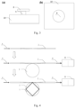
- FIG. 1 is sketch view of a micro-laser of the present invention
- FIG. 2 illustrates a field distribution of a coherently combined mode of a microcavity of the present invention, which is formed by superposition of a fundamental spatial mode and a high-order spatial mode;
- FIG. 3 is a structural view of an ion-doped optical microcavity of the present invention.
- FIG. 4 is a flow chart for coupling an optical fiber cone and the ion-doped optical microcavity of the present invention.
- FIG. 5 is a flow chart for coupling an optical waveguide and an optical microcavity containing quantum dots of the present invention.
- a single-mode micro-laser which is formed by coupling and packaging an optical fiber cone or an optical waveguide and a single whispering gallery mode optical microcavity.
- one optical fiber cone 2 or one optical waveguide 3 is coupled with an on-chip single whispering gallery mode optical microcavity 1 , so as to realize single-mode lasing with a low threshold and a narrow line width based on a high-quality coherently combined mode 5 with a quadrilateral geometry.
- a platform material of the optical microcavity is doped with rare earth ions or organic macromolecules of a certain concentration, or films such as crystals containing quantum dots, silicon dioxide, silicon, III-V compound semiconductor materials and silicon nitride, wherein a lithium niobate film doped with 1 mol % erbium ions and a lithium niobate film containing quantum dots will be further described to illustrate the present invention, but the claims of the present invention should not be limited thereby.
- FIG. 3 A structure of the optical microcavity (specifically a micro-disk cavity) is shown in FIG. 3 , wherein part (a) is a cross-sectional view, and part (b) is a top view of the part (a).
- a heat stretching method for preparing the optical fiber cone 2 comprises steps of: first stripping a polymer layer of a standard single-mode optical fiber; cleaning the optical fiber and heating with hydrogen-oxygen flame, meanwhile stretching both ends of the optical fiber with a translation stage, so that a heated portion of the optical fiber is thinned; controlling a stretching time to obtain the required optical fiber cone.
- a diameter of the optical fiber cone to be used is about 2 microns.
- the pump threshold is determined by the Q factor and mode volume of the microcavities and the gain coefficient of the gain material, which comprises specific steps of: attaching the waist of the optical fiber cone to an edge of the optical microcavity, and inputting the pump light into one end of the optical fiber cone; restricting a wavelength of the pump light within an absorption spectrum wide range of the gain material;
- the optical microcavity 1 displays a coherently combined mode 5 with a polygonal configuration within an absorption range of the gain material, wherein the coherently combined mode is formed by superposition of a fundamental spatial mode and high-order spatial modes, and is identical to the polygonal configuration in the step 4, wherein at this time, the pump light resonates with the coherently combined mode within the absorption spectrum of the gain material, and a lasing light resonates with a coherently combined mode within a fluorescence spectrum of the gain material.
- FIG. 5 coupling of an optical waveguide and an optical microcavity containing quantum dots is illustrated.
- the pump threshold is determined by the Q factor and mode volume of the microcavities and the gain coefficient of the gain material, which comprises specific steps of: attaching the optical waveguide to an edge of the optical microcavity, and inputting the pump light into one end of the optical waveguide; restricting a wavelength of the pump light within the absorption spectrum wide range of the gain material.
- the optical microcavity displays a coherently combined mode with a polygonal configuration within an absorption range of the gain material, wherein the coherently combined mode is formed by superposition of a fundamental spatial mode and a high-order spatial mode, and is identical to the polygonal configuration in the step 4, wherein at this time, the pump light resonates with the coherently combined mode within the absorption spectrum of the gain material, and a lasing light resonates with a coherently combined mode within a fluorescence spectrum of the gain material.
Abstract
A single-mode micro-laser based on a single whispering gallery mode optical microcavity and a preparation method thereof described includes: preparing a desired single whispering gallery mode optical microcavity doped with rare earth ions or containing a gain material such as quantum dots, wherein an optical microcavity configuration include a micro-disk cavity, a ring-shaped microcavity, and a racetrack-shaped microcavity; a material type include lithium niobate, silicon dioxide, silicon nitride, etc.; preparing an optical fiber cone or an optical waveguide of a required size which can excite high-order modes of the optical microcavity, such as a ridge waveguide and a circular waveguides; and coupling, integrating, and packaging the optical fiber cone or the optical waveguide with the microcavity. A pump light is coupled to the optical fiber cone or the optical waveguide to excite a compound mode with a polygonal configuration.
Description
The present invention claims priority under 35 U.S.C. 119(a-d) to CN 202110521827.7, filed May 13, 2021.
The present invention relates to preparation of a single-mode micro-lasers, and more particularly to a single-mode narrow-linewidth laser based on a single whispering gallery mode optical microcavity and a preparation method thereof, wherein dry etching is applied to film materials such as crystal, silicon dioxide, silicon, compound semiconductor materials and silicon nitride doped with a certain concentration of rare earth ions or organic macromolecules or containing quantum dots, and chemical polishing technology is also adopted, so as to obtain an active optical microcavity with a low loss and a high Q value. Finally, through coupling and integration of an optical fiber cone or an optical waveguide, the single-mode micro-laser with a narrow line width and a low threshold can be obtained.
Integrated optical path is designed to miniaturize and integrate optical devices and optical paths on a substrate, so as to reduce the size, energy consumption, and time delay of the optical system, as well as improve performance of the optical system such as stability and processing speed. It is expected to break through the energy consumption and bandwidth bottlenecks faced by conventional optical information processing systems. Micro-lasers, especially single-mode micro-lasers with narrow linewidths, are one of the most important optical devices for constructing integrated optical paths, which have important applications in laser communication, precision measurement, and biosensing (L. He, et al., Nature Nanotechnol. Vol. 6, P 428-432, 2011). Conventionally, micro-lasers are usually prepared based on photonic crystal microcavities, Fabry-Perot microcavities and whispering gallery mode optical microcavities. Among them, the whispering gallery mode optical microcavity can realize confinement of the photons through continuous total internal reflection of light at the interface between the cavity material and the surrounding material with lower refractive index, which has a high quality factor and a small mode volume (DK Armani, et al., Nature Vol. 421, P 925-928, 2003). Therefore, the micro-laser based on the whispering gallery mode optical microcavity has the advantages of low threshold and narrow line width. For single-mode lasing, the size of the whispering gallery mode optical microcavity (hereinafter referred to as optical microcavity) is usually required to be in the sub-micron order to suppress the mode numbers, which inevitably increases the bending radiation loss of the microcavity, reduces the quality factor of the microcavity, and significantly increases the pump threshold and laser linewidth of the micro-laser.
Conventionally, in order to overcome the above defects, a commonly used effective method is to take advantage of the vernier effect of two coupled optical microcavities, so as to excite only the whispering gallery mode shared by the two microcavities, thereby obtaining single-mode lasing with low threshold and narrow linewidth (G. Griffel, IEEE Photon. Technol. Lett. Vol 12, P 1642-1644, 2000; L. Shang, et al., Opt. Lett. Vol. 33, P 1150-1152, 2008). However, the preparation process is complicated and such method is unsuitable for cost-effective preparation. Preparing a single-mode micro-laser with low threshold and narrow linewidth based on single optical microcavity has become an urgent need to improve the application level of optoelectronic integration technology.
An object of the present invention is to provide to overcome challenges of conventional on-chip single-mode micro-laser preparation and provide a single-mode micro-laser based on a single whispering gallery mode optical microcavity. The single-mode micro-laser has a simple preparation process, a low threshold and a narrow line width.
Accordingly, in order to accomplish the above objects, the present invention provides:
a preparation method of a single-mode micro-laser based on a single whispering gallery mode optical microcavity, comprising steps of:
1: preparing an optical microcavity containing a gain material by dry etching, wherein the optical microcavity is the whispering gallery mode optical microcavity; a free spectral range of the optical microcavity is at least ½ of a spectral width of the gain material; the gain material is rare earth ions, quantum dots, or organic macromolecular luminescent materials; a cavity material of the optical microcavity is crystals, silicon dioxides, silicon, III-V compound semiconductor materials or silicon nitride films;
2: preparing an optical fiber cone:
stripping a polymer layer of a standard single-mode optical fiber; cleaning the optical fiber and heating with hydrogen-oxygen flame, meanwhile stretching both ends of the optical fiber with a translation stage, so that a heated portion of the optical fiber is thinned to obtain the required optical fiber cone, and a thinned position is called a waist;
3: performing a coupling test on the optical microcavity and the optical fiber cone, and coupling a pump light, whose pump power is greater than a pump threshold, into the optical fiber cone; wherein the pump threshold is determined by a Q factor and a mode volume of the optical microcavity and a gain coefficient of the gain material, which comprises specific steps of: attaching the waist of the optical fiber cone to an edge of the optical microcavity, and inputting the pump light into one end of the optical fiber cone; restricting a wavelength of the pump light within an absorption spectrum wide range of the gain material;
4: continuously scanning the wavelength of the pump light within the absorption spectrum wide range of the gain material and adjusting or controlling a lateral coupling position of the optical fiber cone and the optical microcavity; observing the optical microcavity in real time through charge coupled device microscopic imaging until a coherently combined mode with a polygonal configuration appears at a pump wavelength, wherein the coherently combined mode is formed by superposition of a fundamental spatial mode and high-order spatial modes; then obtaining a Q value of the optical microcavity when the polygonal configuration appears through a transmission spectrum with a weak pump power, wherein the Q factor of the fundamental spatial mode of the optical microcavity is at least 2 times lower than the Q value of a polygonal mode;
5: fixing the wavelength of the pump light and continuously adjusting the pump power of the pump light until the optical microcavity displays a coherently combined composite mode with a polygonal configuration within an absorption range of the gain material, wherein the coherently combined mode is formed by superposition of a fundamental longitudinal spatial mode and a high-order longitudinal spatial modes, and is identical to the polygonal configuration in the step 4, wherein at this time, the pump light resonates with the coherently combined mode within the absorption spectrum of the gain material, and a lasing light resonates with a coherently combined mode within a fluorescence spectrum of the gain material;
6: coupling the lasing light from an output end of the optical fiber cone, and testing a spectrum and a line width of the lasing light with a spectrum analyzer, wherein the output power of the micro-laser from the optical fiber cone increases linearly with the pump power; obtaining the pump threshold at an inflection point on a calculated growth curve; and
7: fixing, integrating and packaging the optical fiber cone and the optical microcavity to obtain the single-mode micro-laser based on the single whispering gallery mode optical microcavity.
Alternatively, a preparation method of a single-mode micro-laser based on a single whispering gallery mode optical microcavity is provided, comprising steps of:
1: preparing an optical microcavity containing a gain material by dry etching, wherein the optical microcavity is the whispering gallery mode optical microcavity; a free spectral range of the optical microcavity is at least ½ of a spectral width of the gain material; the gain material is rare earth ions, quantum dots, or organic macromolecular luminescent materials; a cavity material of the optical microcavity is crystals, silicon dioxides, silicon, III-V compound semiconductor materials or silicon nitride films;
2: preparing a required optical waveguide by photolithography assisted dry etching to simultaneously accommodate high-order mode transmission and excite a high-order mode of the optical microcavity within an absorption spectrum wide range and a gain spectrum wide range of the gain material;
3: performing a coupling test on the optical microcavity and the optical waveguide, and coupling a pump light, whose pump power is greater than a pump threshold, into the optical waveguide; wherein the pump threshold is determined by a Q factor and a mode volume of the optical microcavity and a gain coefficient of the gain material, which comprises specific steps of: attaching the optical waveguide to an edge of the optical microcavity, and inputting the pump light into one end of the optical waveguide; restricting a wavelength of the pump light within the absorption spectrum wide range of the gain material; continuously increasing the pump power of the pump light, wherein when the pump power of the pump light is greater than the pump threshold, the output power of the micro-laser from the optical waveguide increases linearly with the pump power; obtaining the pump threshold at an inflection point on a calculated growth curve;
4: continuously scanning the wavelength of the pump light within the absorption spectrum wide range of the gain material, and adjusting or controlling a spatial position of the optical waveguide and the optical microcavity to excite fundamental and high-order spatial modes within the microcavities; observing the optical microcavity in real time through charge coupled device microscopic imaging until a coherently combined mode with a polygonal configuration appears at pump wavelength, wherein the coherently combined mode is formed by superposition of a fundamental spatial mode and high-order spatial modes; then obtaining a Q value of the optical microcavity when the polygonal configuration appears through a transmission spectrum with weak pump power; and the Q factor of the fundamental spatial mode is at least 2 times lower than the Q factor of the coherently combined mode;
5: fixing the wavelength of the pump light and continuously adjusting the pump power of the pump light until the optical microcavity displays a coherently combined mode with a polygonal configuration within an absorption range of the gain material, wherein at this time, the pump light resonates with the coherently combined mode within the absorption spectrum of the gain material, and a lasing light resonates with a coherently combined mode within a fluorescence spectrum of the gain material;
6: coupling the lasing light from an output end of the optical waveguide, and testing a spectrum and a line width of the lasing light with a spectrum analyzer until a lasing with a single-mode, a narrow line width, and a low-threshold is obtained; where the output power of the micro-laser from the optical fiber cone increases linearly with the pump power; obtaining the pump threshold at an inflection point on a calculated growth curve; and
7: fixing, integrating and packaging the optical waveguide and the optical microcavity to obtain the single-mode micro-laser based on the single whispering gallery mode optical microcavity.
The single-mode micro-laser based on the single whispering gallery mode optical microcavity prepared by the above preparation methods comprises the single whispering gallery mode optical microcavity containing an active material, and the optical fiber cone or the optical waveguide, wherein the active material is rare earth ions, quantum dots, or organic macromolecular luminescent materials; the cavity material of the optical microcavity is crystals, silicon dioxides, silicon, III-V compound semiconductor materials or silicon nitride films; a line width of the single-mode micro-laser is most 1 megahertz, and a threshold is at most 1 milliwatt.
The present invention utilizes the optical fiber cone or the optical waveguide that can support the high-order spatial mode transmission to couple with the optical microcavity. By adjusting the coupling position, the quality factor of the fundamental spatial mode of the optical microcavity is selectively reduced. At the same time, the polygonal coherently combined mode with the high quality factor in the optical microcavity, which is formed by the superposition of the fundamental spatial mode and the high-order spatial mode, is effectively excited. Furthermore, the pump light and the lasing light are resonant with the coherently combined modes, respectively, so as to obtain a single-mode lasing with the low threshold and the narrow line width.
Beneficial effects of the present invention are that: the single whispering gallery mode optical microcavity is used to prepare the single-mode micro-laser with the low threshold and the narrow line width, and to promote development of related high-tech industries. A platform material of the optical microcavity is doped with rare earth ions or organic macromolecules of a certain concentration, or films such as crystals containing quantum dots, silicon dioxide, silicon, III-V compound semiconductor materials and silicon nitride. By using the optical fiber cone with high transmittance and precisely controlled size (Y. Xu, et al., Opt. Express Vol. 25, P 10434-10440, 2017) or the optical waveguide which is easy to be integrated on chip, the polygonal configuration coherently combined mode formed by superposition of the fundamental spatial mode and the high-order spatial mode in the optical microcavity is excited, and a quality factor of an normal mode of the optical microcavity is reduced. Only one coherently combined mode can be excited in the free spectral range, and such mode is basically unaffected by coupling effect of the optical fiber cone or the optical waveguide. Therefore, the high quality factor is maintained. Under mode competition, only the coherently combined mode is cable of lasing, so the single-mode lasing with the low threshold and the narrow line width can be obtained.
The present invention will be further illustrated with the following embodiments and accompanying drawings, but the protection scope of the present invention should not be limited thereby.
Referring to FIG. 1 , a single-mode micro-laser is provided, which is formed by coupling and packaging an optical fiber cone or an optical waveguide and a single whispering gallery mode optical microcavity. As an example of the present invention, one optical fiber cone 2 or one optical waveguide 3 is coupled with an on-chip single whispering gallery mode optical microcavity 1, so as to realize single-mode lasing with a low threshold and a narrow line width based on a high-quality coherently combined mode 5 with a quadrilateral geometry. A platform material of the optical microcavity is doped with rare earth ions or organic macromolecules of a certain concentration, or films such as crystals containing quantum dots, silicon dioxide, silicon, III-V compound semiconductor materials and silicon nitride, wherein a lithium niobate film doped with 1 mol % erbium ions and a lithium niobate film containing quantum dots will be further described to illustrate the present invention, but the claims of the present invention should not be limited thereby.
1) Coupling an optical fiber cone to a lithium niobate film optical microcavity doped with erbium ions, wherein referring to FIG. 4 , a wafer of a lithium niobate film 8 doped with 1 mol % erbium ions is illustrated; plating a 700 nm-thick chromium film as a mask, and etching the optical microcavity of a required size by a femtosecond laser; wherein the optical microcavity has a diameter of about 30 microns, and is located on a 2 μm-thick silicon dioxide layer pillar 9 supported by a underlying lithium niobate substrate 10; a free spectral range of the optical microcavity near a wavelength of 1550 nm is about 13 nm, which is about half of an erbium ion gain bandwidth (1535˜1560 nm); processing the optical microcavity etched by the femtosecond laser with a chemical mechanical polishing technology (R. Wu, et al., Opt. Lett., Vol. 43, P 4116-4118, 2018) to obtain a whispering gallery mode optical microcavity 1 which has a smooth edge and is doped with the erbium ions, then performing auxiliary polishing with a polishing liquid containing 60 nm silica beads, wherein after polishing, a golden velvet polishing pad is used for carefully cleaning, so as to prevent small particles from scratching the optical microcavity, and an ultrasonic method can be used for deep cleaning; cleaning the polished optical microcavity by ultrasonic and cotton swab scrubbing methods to remove organic matters and particles on the surface, making a surface of the optical microcavity cleaner and reducing loss. A structure of the optical microcavity (specifically a micro-disk cavity) is shown in FIG. 3 , wherein part (a) is a cross-sectional view, and part (b) is a top view of the part (a).
2) preparing an optical fiber cone with a size that can excite a fundamental spatial mode and a high-order spatial mode of the optical microcavity 2; wherein a heat stretching method for preparing the optical fiber cone 2 comprises steps of: first stripping a polymer layer of a standard single-mode optical fiber; cleaning the optical fiber and heating with hydrogen-oxygen flame, meanwhile stretching both ends of the optical fiber with a translation stage, so that a heated portion of the optical fiber is thinned; controlling a stretching time to obtain the required optical fiber cone. A diameter of the optical fiber cone to be used is about 2 microns.
3) after the optical microcavity 1 and the optical fiber cone 2 are prepared, performing a coupling test on the optical microcavity 1 and the optical fiber cone 2; adjusting a pump power of a pump light and coupling the pump light, whose pump power is greater than a pump threshold, into one end of the optical fiber cone; wherein the pump threshold is determined by the Q factor and mode volume of the microcavities and the gain coefficient of the gain material, which comprises specific steps of: attaching the waist of the optical fiber cone to an edge of the optical microcavity, and inputting the pump light into one end of the optical fiber cone; restricting a wavelength of the pump light within an absorption spectrum wide range of the gain material;
4) continuously scanning the wavelength of the pump light within the absorption spectrum wide range of the gain material and adjusting or controlling a lateral coupling position of the optical fiber cone and the optical microcavity; observing the optical microcavity in real time through charge coupled device microscopic imaging until a coherently combined mode with a polygonal configuration (quadrilateral) appears at pump wavelength, wherein the coherently combined mode is formed by superposition of a fundamental spatial mode and high-order spatial modes; then obtaining a Q value of the optical microcavity when the polygonal configuration appears through a transmission spectrum with weak pump power, where the Q factor of the fundamental spatial mode of the optical microcavity is at least 2 times lower than the Q value of the polygonal mode.
5) fixing the wavelength of the pump light and adjusting the pump power of the pump light 4 until the optical microcavity 1 displays a coherently combined mode 5 with a polygonal configuration within an absorption range of the gain material, wherein the coherently combined mode is formed by superposition of a fundamental spatial mode and high-order spatial modes, and is identical to the polygonal configuration in the step 4, wherein at this time, the pump light resonates with the coherently combined mode within the absorption spectrum of the gain material, and a lasing light resonates with a coherently combined mode within a fluorescence spectrum of the gain material.
6) coupling the lasing light 6 from an output end of the optical fiber cone 2, and testing a spectrum and a line width of the lasing light 6 with a spectrum analyzer 11 until a lasing with a single-mode, a narrow line width, and a low-threshold is obtained.
7) fixing, integrating and packaging the optical fiber cone 2 and the optical microcavity 1 to assemble a portable single-mode micro-laser 7 with a narrow line width (less than 10000 Hz) and a low threshold (80 microwatts).
Referring to FIG. 5 , coupling of an optical waveguide and an optical microcavity containing quantum dots is illustrated.
1) Etching the optical microcavity containing the quantum dots of a required size by a femtosecond laser; wherein after etching a free spectral range of the optical microcavity is at least ½ of a spectral width of a material containing the quantum dots; processing the optical microcavity with a chemical mechanical polishing technology (R. Wu, et al., Opt. Lett., Vol. 43, P 4116-4118, 2018) to obtain an optical microcavity with a smooth edge, wherein before polishing, a golden velvet polishing pad is used for carefully cleaning, so as to prevent small particles from scratching the optical microcavity, and an ultrasonic method can be used for deep cleaning; cleaning the polished optical microcavity by ultrasonic and cotton swab scrubbing methods to remove organic matters and particles on the surface, making a surface of the optical microcavity cleaner and reducing loss.
2) preparing a required optical waveguide by photolithography assisted dry etching and the chemo mechanical polishing technology to simultaneously accommodate high-order mode transmission and excite high-order modes of the optical microcavity within an absorption spectrum wide range and a gain spectrum wide range of the gain material; wherein a chemical mechanical polishing method can make two sides of the optical waveguide smoother (observable under a microscope) and reduce loss; cleaning the polishing pad before polishing to prevent particles from scratching the optical waveguide, and cleaning the polished optical waveguide for subsequent use. 3) performing a coupling test on the optical microcavity and the optical waveguide, and coupling a pump light, whose pump power is greater than a pump threshold, into the optical waveguide; wherein the pump threshold is determined by the Q factor and mode volume of the microcavities and the gain coefficient of the gain material, which comprises specific steps of: attaching the optical waveguide to an edge of the optical microcavity, and inputting the pump light into one end of the optical waveguide; restricting a wavelength of the pump light within the absorption spectrum wide range of the gain material.
4) coupling the pump light within the absorption spectrum wide range of the gain material to the optical waveguide, so as to be coupled with the microcavity; and adjusting or controlling a spatial position of the optical waveguide and the optical microcavity to excite fundamental and high-order spatial modes within the microcavities; continuously scanning the wavelength of the pump light; observing the optical microcavity in real time through charge coupled device microscopic imaging until a coherently combined mode with a polygonal configuration (triangular) appears at pump wavelength, wherein the coherently combined mode is formed by superposition of a fundamental spatial mode and high-order spatial modes; then obtaining a Q value of the optical microcavity when the polygonal configuration appears through a transmission spectrum with weak pump power; and the Q factor of the fundamental spatial mode is at least 2 times lower than the Q factor of the coherently combined mode.
5) fixing the wavelength of the pump light 4 and continuously adjusting the pump power of the pump light within the gain spectrum wide range of the gain material until the optical microcavity displays a coherently combined mode with a polygonal configuration within an absorption range of the gain material, wherein the coherently combined mode is formed by superposition of a fundamental spatial mode and a high-order spatial mode, and is identical to the polygonal configuration in the step 4, wherein at this time, the pump light resonates with the coherently combined mode within the absorption spectrum of the gain material, and a lasing light resonates with a coherently combined mode within a fluorescence spectrum of the gain material.
6) coupling the lasing light 6 from an output end of the optical waveguide 3, and testing a spectrum and a line width of the lasing light 6 with a spectrum analyzer 11 until a lasing with a single-mode, a narrow line width, and a low-threshold is obtained.
7) fixing, integrating and packaging the optical waveguide 3 and the optical microcavity 1 to assemble a portable single-mode micro-laser 7 with a narrow line width (less than 10000 Hz) and a low threshold (80 microwatts).
Claims (6)
1. A preparation method of a single-mode micro-laser based on a single whispering gallery mode optical microcavity, comprising steps of:
1: preparing an optical microcavity containing a gain material by dry etching, wherein the optical microcavity is the whispering gallery mode optical microcavity; a free spectral range of the optical microcavity is at least ½ of a spectral width of the gain material; the gain material is rare earth ions, quantum dots, or organic macromolecular luminescent materials; a cavity material of the optical microcavity is crystals, silicon dioxides, silicon, III-V compound semiconductor materials or silicon nitride films;
2: preparing an optical fiber cone:
stripping a polymer layer of a standard single-mode optical fiber; cleaning the optical fiber and heating with hydrogen-oxygen flame, meanwhile stretching both ends of the optical fiber with a translation stage, so that a heated portion of the optical fiber is thinned to obtain the optical fiber cone, and a thinned position is called a waist;
3: performing a coupling test on the optical microcavity and the optical fiber cone, and coupling a pump light, whose pump power is greater than a pump threshold, into the optical fiber cone; wherein the pump threshold is determined by a Q factor and a mode volume of the optical microcavity and a gain coefficient of the gain material, which comprises specific steps of: attaching the waist of the optical fiber cone to an edge of the optical microcavity, and inputting the pump light into one end of the optical fiber cone; restricting a wavelength of the pump light within an absorption spectrum wide range of the gain material;
4: continuously scanning the wavelength of the pump light within the absorption spectrum wide range of the gain material and adjusting or controlling a lateral coupling position of the optical fiber cone and the optical microcavity; observing the optical microcavity in real time through charge coupled device microscopic imaging until a coherently combined mode with a polygonal configuration appears at a pump wavelength, wherein the coherently combined mode is formed by superposition of a fundamental spatial mode and high-order spatial modes; then obtaining the Q factor of the optical microcavity when the polygonal configuration appears through a transmission spectrum; wherein the Q factor of the fundamental spatial mode of the optical microcavity is at least 2 times lower than the Q factor of a polygonal mode;
5: fixing the wavelength of the pump light and continuously adjusting the pump power of the pump light until the optical microcavity displays a coherently combined mode with a polygonal configuration within an absorption range of the gain material, wherein the coherently combined mode is formed by superposition of a fundamental spatial mode and high-order spatial modes, and is identical to the polygonal configuration in the step 4, wherein at this time, the pump light resonates with the coherently combined mode within the absorption spectrum of the gain material, and a lasing light resonates with a coherently combined mode within a fluorescence spectrum of the gain material;
6: coupling the lasing light from an output end of the optical fiber cone, and testing a spectrum and a line width of the lasing light with a spectrum analyzer until a lasing with a single-mode is obtained; and
7: fixing, integrating and packaging the optical fiber cone and the optical microcavity to obtain the single-mode micro-laser based on the single whispering gallery mode optical microcavity.
2. A preparation method of a single-mode micro-laser based on a single whispering gallery mode optical microcavity, comprising steps of:
1: preparing an optical microcavity containing a gain material by dry etching, wherein the optical microcavity is the whispering gallery mode optical microcavity; a free spectral range of the optical microcavity is at least ½ of a spectral width of the gain material; the gain material is rare earth ions, quantum dots, or organic macromolecular luminescent materials; a cavity material of the optical microcavity is crystals, silicon dioxides, silicon, III-V compound semiconductor materials or silicon nitride films;
2: preparing an optical waveguide by photolithography assisted dry etching to simultaneously accommodate high-order mode transmission and excite a high-order mode of the optical microcavity within an absorption spectrum wide range and a gain spectrum wide range of the gain material;
3: performing a coupling test on the optical microcavity and the optical waveguide, and coupling a pump light, whose pump power is greater than a pump threshold, into the optical waveguide; wherein the pump threshold is determined by a Q factor and a mode volume of the optical microcavity and a gain coefficient of the gain material, which comprises specific steps of: attaching the optical waveguide to an edge of the optical microcavity, and inputting the pump light into one end of the optical waveguide; restricting a wavelength of the pump light within the absorption spectrum wide range of the gain material;
4: continuously scanning the wavelength of the pump light within the absorption spectrum wide range of the gain material, and adjusting or controlling a spatial position of the optical waveguide and the optical microcavity to excite fundamental and high-order spatial modes within the optical microcavity; observing the optical microcavity in real time through charge coupled device microscopic imaging until a coherently combined mode with a polygonal configuration appears at a pump wavelength, wherein the coherently combined mode is formed by superposition of a fundamental spatial mode and high-order spatial modes; then obtaining the Q factor of the optical microcavity when the polygonal configuration appears through a transmission spectrum; and the Q factor of the fundamental spatial mode is at least 2 times lower than the Q factor of the coherently combined mode;
5: fixing the wavelength of the pump light and continuously adjusting the pump power of the pump light until the optical microcavity displays a coherently combined mode with a polygonal configuration within an absorption range of the gain material, wherein the coherently combined mode is formed by superposition of a fundamental spatial mode and a high-order spatial mode, and is identical to the polygonal configuration in the step 4, wherein at this time, the pump light resonates with the coherently combined mode within the absorption spectrum of the gain material, and a lasing light resonates with a coherently combined mode within a fluorescence spectrum of the gain material;
6: coupling the lasing light from an output end of the optical waveguide, and testing a spectrum and a line width of the lasing light with a spectrum analyzer until a lasing with a single-mode is obtained; and
7: fixing, integrating and packaging the optical waveguide and the optical microcavity to obtain the single-mode micro-laser based on the single whispering gallery mode optical microcavity.
3. The single-mode micro-laser based on the single whispering gallery mode optical microcavity prepared by the preparation method as recited in claim 1 .
4. The single-mode micro-laser based on the single whispering gallery mode optical microcavity prepared by the preparation method as recited in claim 2 .
5. The single-mode micro-laser, as recited in claim 3 , comprising: the single whispering gallery mode optical microcavity containing an active material, and the optical fiber cone or the optical waveguide, wherein the active material is rare earth ions, quantum dots, or organic macromolecular luminescent materials; the cavity material of the optical microcavity is crystals, silicon dioxides, silicon, III-V compound semiconductor materials or silicon nitride films; a line width of the single-mode micro-laser is less than 1 megahertz, and a threshold is less than 1 milliwatt.
6. The single-mode micro-laser, as recited in claim 4 , comprising: the single whispering gallery mode optical microcavity containing an active material, and the optical fiber cone or the optical waveguide, wherein the active material is rare earth ions, quantum dots, or organic macromolecular luminescent materials; the cavity material of the optical microcavity is crystals, silicon dioxides, silicon, III-V compound semiconductor materials or silicon nitride films; a line width of the single-mode micro-laser is less than 1 megahertz, and a threshold is less than 1 milliwatt.
Applications Claiming Priority (2)
| Application Number | Priority Date | Filing Date | Title |
|---|---|---|---|
| CN202110521827.7A CN113507039B (en) | 2021-05-13 | 2021-05-13 | Single-mode micro-laser based on single whispering gallery mode optical microcavity and implementation method |
| CN202110521827.7 | 2021-05-13 |
Publications (2)
| Publication Number | Publication Date |
|---|---|
| US20210367402A1 US20210367402A1 (en) | 2021-11-25 |
| US11600968B2 true US11600968B2 (en) | 2023-03-07 |
Family
ID=78008470
Family Applications (1)
| Application Number | Title | Priority Date | Filing Date |
|---|---|---|---|
| US17/397,992 Active 2041-10-06 US11600968B2 (en) | 2021-05-13 | 2021-08-10 | Single-mode micro-laser based on single whispering gallery mode optical microcavity and preparation method thereof |
Country Status (2)
| Country | Link |
|---|---|
| US (1) | US11600968B2 (en) |
| CN (1) | CN113507039B (en) |
Families Citing this family (6)
| Publication number | Priority date | Publication date | Assignee | Title |
|---|---|---|---|---|
| CN114089473B (en) * | 2021-11-24 | 2023-08-22 | 深圳技术大学 | On-chip microcavity photon integrated chip structure and preparation method thereof |
| CN115290558A (en) * | 2022-01-30 | 2022-11-04 | 浙江师范大学 | CRDS gas detection device and method based on high-Q-value microcavity laser |
| CN115014599B (en) * | 2022-04-21 | 2023-06-02 | 深圳大学 | Method for preparing whispering gallery mode microbubble probe resonator by carbon dioxide laser, resonator and pressure sensing system |
| CN114951961B (en) * | 2022-05-17 | 2023-03-07 | 电子科技大学 | Preparation method of few-mode stable-coupling WGM (micro waveguide graticule) optical micro-rod cavity |
| CN116131075B (en) * | 2022-12-29 | 2024-01-05 | 南京大学 | Octave optical comb generation system and method based on scattered waves |
| CN116073219B (en) * | 2023-04-07 | 2023-06-06 | 南京邮电大学 | Preparation method of all-inorganic perovskite liquid laser based on micro-flow channel |
Citations (9)
| Publication number | Priority date | Publication date | Assignee | Title |
|---|---|---|---|---|
| US20010033587A1 (en) * | 2000-03-09 | 2001-10-25 | California Institute Of Technology | Micro-cavity laser |
| US6711200B1 (en) * | 1999-09-07 | 2004-03-23 | California Institute Of Technology | Tuneable photonic crystal lasers and a method of fabricating the same |
| US20040179573A1 (en) * | 2002-10-02 | 2004-09-16 | California Institute Of Technology | Ultra-high Q micro-resonator and method of fabrication |
| US20110163421A1 (en) * | 2010-01-04 | 2011-07-07 | The Royal Institution For The Advancement Of Learning / Mcgill University | Method for Fabricating Optical Semiconductor Tubes and Devices Thereof |
| US20110188525A1 (en) * | 2008-06-13 | 2011-08-04 | Julien Claudon | Terahertz wave emission laser device |
| US20120320939A1 (en) * | 2010-02-24 | 2012-12-20 | Roeland Baets | Laser light coupling into soi cmos photonic integrated circuit |
| US20150092808A1 (en) * | 2011-06-17 | 2015-04-02 | Jiang Li | Chip-based laser resonator device for highly coherent laser generation |
| US20190346625A1 (en) * | 2018-05-08 | 2019-11-14 | Shanghai Institute of Optics And Fine Mechanics, Chiness Academy of Sciences | Method for preparing film micro-optical structure based on photolithography and chemomechanical polishing |
| US20210104861A1 (en) * | 2018-01-29 | 2021-04-08 | Ronald LaComb | Concentric cylindrical circumferential laser |
Family Cites Families (9)
| Publication number | Priority date | Publication date | Assignee | Title |
|---|---|---|---|---|
| CN108899755B (en) * | 2015-07-03 | 2020-07-31 | 安徽大学 | Tunable optical microcavity doped laser |
| CN105098575A (en) * | 2015-07-22 | 2015-11-25 | 南京邮电大学 | Narrow-band fiber laser for mixed medium microcavity full-optical tuning |
| CN106635773B (en) * | 2016-09-29 | 2020-01-21 | 南开大学 | DNA hybridization micro-fluidic detector based on fiber microcavity echo wall |
| CN107046221A (en) * | 2017-02-24 | 2017-08-15 | 南京邮电大学 | A kind of single-frequency narrow band fiber laser based on the high symmetrical microcavity of circularity three-dimensional rotation |
| CN109755850B (en) * | 2019-03-08 | 2020-01-03 | 江苏师范大学 | Intermediate infrared Raman ultrafast fiber laser oscillator based on micro-cavity |
| CN109809685B (en) * | 2019-03-18 | 2022-05-24 | 华南理工大学 | Microcrystalline glass whispering gallery mode resonant cavity capable of outputting single-mode high-performance laser and preparation method thereof |
| CN111129934B (en) * | 2019-11-26 | 2021-10-12 | 华东师范大学 | Microcavity-adjustable optical frequency comb based on lithium niobate and preparation method thereof |
| CN111367019A (en) * | 2020-02-20 | 2020-07-03 | 华东师范大学 | Optical waveguide coupling method based on optical fiber cone |
| CN112268636B (en) * | 2020-09-22 | 2022-06-03 | 北京航空航天大学 | Liquid temperature sensing system based on whispering gallery mode spherical optical microcavity |
-
2021
- 2021-05-13 CN CN202110521827.7A patent/CN113507039B/en active Active
- 2021-08-10 US US17/397,992 patent/US11600968B2/en active Active
Patent Citations (9)
| Publication number | Priority date | Publication date | Assignee | Title |
|---|---|---|---|---|
| US6711200B1 (en) * | 1999-09-07 | 2004-03-23 | California Institute Of Technology | Tuneable photonic crystal lasers and a method of fabricating the same |
| US20010033587A1 (en) * | 2000-03-09 | 2001-10-25 | California Institute Of Technology | Micro-cavity laser |
| US20040179573A1 (en) * | 2002-10-02 | 2004-09-16 | California Institute Of Technology | Ultra-high Q micro-resonator and method of fabrication |
| US20110188525A1 (en) * | 2008-06-13 | 2011-08-04 | Julien Claudon | Terahertz wave emission laser device |
| US20110163421A1 (en) * | 2010-01-04 | 2011-07-07 | The Royal Institution For The Advancement Of Learning / Mcgill University | Method for Fabricating Optical Semiconductor Tubes and Devices Thereof |
| US20120320939A1 (en) * | 2010-02-24 | 2012-12-20 | Roeland Baets | Laser light coupling into soi cmos photonic integrated circuit |
| US20150092808A1 (en) * | 2011-06-17 | 2015-04-02 | Jiang Li | Chip-based laser resonator device for highly coherent laser generation |
| US20210104861A1 (en) * | 2018-01-29 | 2021-04-08 | Ronald LaComb | Concentric cylindrical circumferential laser |
| US20190346625A1 (en) * | 2018-05-08 | 2019-11-14 | Shanghai Institute of Optics And Fine Mechanics, Chiness Academy of Sciences | Method for preparing film micro-optical structure based on photolithography and chemomechanical polishing |
Also Published As
| Publication number | Publication date |
|---|---|
| CN113507039A (en) | 2021-10-15 |
| CN113507039B (en) | 2022-07-08 |
| US20210367402A1 (en) | 2021-11-25 |
Similar Documents
| Publication | Publication Date | Title |
|---|---|---|
| US11600968B2 (en) | Single-mode micro-laser based on single whispering gallery mode optical microcavity and preparation method thereof | |
| EP3072188B1 (en) | Sagnac loop mirror based laser cavity on silicon photonics platform | |
| Liu et al. | Optical amplification and lasing by stimulated Raman scattering in silicon waveguides | |
| US9831635B2 (en) | Quantum dot SOA-silicon external cavity multi-wavelength laser | |
| US7528403B1 (en) | Hybrid silicon-on-insulator waveguide devices | |
| CN111129920A (en) | Preparation method of distributed Bragg reflection laser based on erbium-doped lithium niobate thin film | |
| WO2016138506A2 (en) | Multi-wavelength laser | |
| Bradley et al. | 1.8-µm thulium microlasers integrated on silicon | |
| Li et al. | Optically pumped milliwatt whispering-gallery microcavity laser | |
| Boust et al. | Compact optical frequency comb source based on a DFB butt-coupled to a silicon nitride microring | |
| Wang et al. | Thin-film Lithium Niobate Photonic Devices on 8-inch Silicon Substrates | |
| Boust et al. | Single-mode and multi-mode DBR lasers using InP-Si3N4/SiO2 integration | |
| Pu et al. | AlGaAs-on-insulator nonlinear photonics | |
| Yue et al. | Single photon emissions from InAs/GaAs quantum dots embedded in GaAs/SiO2 hybrid microdisks | |
| Buyukkaya | Integration of Classical/Nonclassical Optical Nonlinearities With Photonic Circuits | |
| Davenport et al. | Efficient and broad band coupling between silicon and ultra-low-loss silicon nitride waveguides | |
| Mendoza-Castro et al. | Compact side-coupled Silicon Nitride Photonic Crystal Nanobeam Cavity for refractive index sensing | |
| Liang et al. | Monolithically integrated waveguide-coupled single-frequency microlaser on erbium-doped thin film lithium niobate | |
| Shankar | Mid-infrared photonics in silicon | |
| Zhang et al. | Ultrahigh-Q lithium niobate microring Resonator | |
| Liu et al. | On-chip Lithium Niobate Heterogeneous Photonic Crystal Nanocavity Laser | |
| Swillo et al. | Characterization and modeling of InP/GaInAsP photonic-crystal waveguides | |
| Bürger et al. | Applying CMOS capabilities of CEITEC´ s foundry towards silicon photonic devices | |
| Xiong | Novel Materials for Active Silicon Photonics | |
| Shoman et al. | A single microring resonator for measuring waveguide losses |
Legal Events
| Date | Code | Title | Description |
|---|---|---|---|
| FEPP | Fee payment procedure |
Free format text: ENTITY STATUS SET TO UNDISCOUNTED (ORIGINAL EVENT CODE: BIG.); ENTITY STATUS OF PATENT OWNER: SMALL ENTITY |
|
| FEPP | Fee payment procedure |
Free format text: ENTITY STATUS SET TO SMALL (ORIGINAL EVENT CODE: SMAL); ENTITY STATUS OF PATENT OWNER: SMALL ENTITY |
|
| STPP | Information on status: patent application and granting procedure in general |
Free format text: DOCKETED NEW CASE - READY FOR EXAMINATION |
|
| STPP | Information on status: patent application and granting procedure in general |
Free format text: NON FINAL ACTION MAILED |
|
| STPP | Information on status: patent application and granting procedure in general |
Free format text: RESPONSE TO NON-FINAL OFFICE ACTION ENTERED AND FORWARDED TO EXAMINER |
|
| STCF | Information on status: patent grant |
Free format text: PATENTED CASE |