US11459290B2 - Compound and organic light emitting device using the same - Google Patents
Compound and organic light emitting device using the same Download PDFInfo
- Publication number
- US11459290B2 US11459290B2 US16/487,404 US201816487404A US11459290B2 US 11459290 B2 US11459290 B2 US 11459290B2 US 201816487404 A US201816487404 A US 201816487404A US 11459290 B2 US11459290 B2 US 11459290B2
- Authority
- US
- United States
- Prior art keywords
- compound
- group
- layer
- light emitting
- preparation
- Prior art date
- Legal status (The legal status is an assumption and is not a legal conclusion. Google has not performed a legal analysis and makes no representation as to the accuracy of the status listed.)
- Active, expires
Links
- YQJZCDPROCFBOQ-UHFFFAOYSA-N CC1(C)c2cc(-c3ccc4c(c3)C3(c5ccccc5-4)c4ccccc4C(C)(C)c4ccccc43)ccc2-c2ccc(N(c3ccccc3)c3ccccc3)cc21.CC1(C)c2ccccc2C2(c3ccccc3-c3c(-c4ccc(N(c5ccccc5)c5ccccc5)c5ccccc45)cccc32)c2ccccc21.CC1(C)c2ccccc2C2(c3ccccc3-c3cc(-c4ccc(N(c5ccccc5)c5ccccc5)c5ccccc45)ccc32)c2ccccc21.CC1(C)c2ccccc2C2(c3ccccc3-c3ccc(-c4ccc(N(c5ccccc5)c5ccccc5)c5ccccc45)cc32)c2ccccc21 Chemical compound CC1(C)c2cc(-c3ccc4c(c3)C3(c5ccccc5-4)c4ccccc4C(C)(C)c4ccccc43)ccc2-c2ccc(N(c3ccccc3)c3ccccc3)cc21.CC1(C)c2ccccc2C2(c3ccccc3-c3c(-c4ccc(N(c5ccccc5)c5ccccc5)c5ccccc45)cccc32)c2ccccc21.CC1(C)c2ccccc2C2(c3ccccc3-c3cc(-c4ccc(N(c5ccccc5)c5ccccc5)c5ccccc45)ccc32)c2ccccc21.CC1(C)c2ccccc2C2(c3ccccc3-c3ccc(-c4ccc(N(c5ccccc5)c5ccccc5)c5ccccc45)cc32)c2ccccc21 YQJZCDPROCFBOQ-UHFFFAOYSA-N 0.000 description 2
- PQPOFHRUTJCNQN-UHFFFAOYSA-N CC1(C)c2ccccc2-c2ccc(N(c3ccc(-c4ccc5c(c4)C4(c6ccccc6-5)c5ccccc5C(C)(C)c5ccccc54)cc3)c3cc(-c4ccccc4)cc(-c4ccccc4)c3)cc21.CC1(C)c2ccccc2-c2ccc(N(c3ccc(-c4ccc5c(c4)C4(c6ccccc6-5)c5ccccc5C(C)(C)c5ccccc54)cc3)c3cccc(-c4ccccc4)c3)cc21.CC1(C)c2ccccc2-c2ccc(N(c3ccc(-c4ccc5c(c4)C4(c6ccccc6-5)c5ccccc5C(c5ccccc5)(c5ccccc5)c5ccccc54)cc3)c3cc(-c4ccccc4)cc(-c4ccccc4)c3)cc21.CC1(C)c2ccccc2-c2ccc(N(c3ccc(-c4ccc5c(c4)C4(c6ccccc6-5)c5ccccc5C(c5ccccc5)(c5ccccc5)c5ccccc54)cc3)c3cccc(-c4ccccc4)c3)cc21 Chemical compound CC1(C)c2ccccc2-c2ccc(N(c3ccc(-c4ccc5c(c4)C4(c6ccccc6-5)c5ccccc5C(C)(C)c5ccccc54)cc3)c3cc(-c4ccccc4)cc(-c4ccccc4)c3)cc21.CC1(C)c2ccccc2-c2ccc(N(c3ccc(-c4ccc5c(c4)C4(c6ccccc6-5)c5ccccc5C(C)(C)c5ccccc54)cc3)c3cccc(-c4ccccc4)c3)cc21.CC1(C)c2ccccc2-c2ccc(N(c3ccc(-c4ccc5c(c4)C4(c6ccccc6-5)c5ccccc5C(c5ccccc5)(c5ccccc5)c5ccccc54)cc3)c3cc(-c4ccccc4)cc(-c4ccccc4)c3)cc21.CC1(C)c2ccccc2-c2ccc(N(c3ccc(-c4ccc5c(c4)C4(c6ccccc6-5)c5ccccc5C(c5ccccc5)(c5ccccc5)c5ccccc54)cc3)c3cccc(-c4ccccc4)c3)cc21 PQPOFHRUTJCNQN-UHFFFAOYSA-N 0.000 description 2
- GMSGKSJJABGKTJ-UHFFFAOYSA-N CC1(C)c2ccccc2-c2ccc(N(c3ccc(-c4ccc5c(c4)C4(c6ccccc6-5)c5ccccc5C(C)(C)c5ccccc54)cc3)c3ccc(-c4ccccc4)cc3-c3ccccc3)cc21.CC1(C)c2ccccc2-c2ccc(N(c3ccc(-c4ccc5c(c4)C4(c6ccccc6-5)c5ccccc5C(C)(C)c5ccccc54)cc3)c3ccccc3-c3ccccc3)cc21.CC1(C)c2ccccc2-c2ccc(N(c3ccc(-c4ccc5c(c4)C4(c6ccccc6-5)c5ccccc5C(c5ccccc5)(c5ccccc5)c5ccccc54)cc3)c3ccc(-c4ccccc4)cc3-c3ccccc3)cc21.CC1(C)c2ccccc2-c2ccc(N(c3ccc(-c4ccc5c(c4)C4(c6ccccc6-5)c5ccccc5C(c5ccccc5)(c5ccccc5)c5ccccc54)cc3)c3ccccc3-c3ccccc3)cc21 Chemical compound CC1(C)c2ccccc2-c2ccc(N(c3ccc(-c4ccc5c(c4)C4(c6ccccc6-5)c5ccccc5C(C)(C)c5ccccc54)cc3)c3ccc(-c4ccccc4)cc3-c3ccccc3)cc21.CC1(C)c2ccccc2-c2ccc(N(c3ccc(-c4ccc5c(c4)C4(c6ccccc6-5)c5ccccc5C(C)(C)c5ccccc54)cc3)c3ccccc3-c3ccccc3)cc21.CC1(C)c2ccccc2-c2ccc(N(c3ccc(-c4ccc5c(c4)C4(c6ccccc6-5)c5ccccc5C(c5ccccc5)(c5ccccc5)c5ccccc54)cc3)c3ccc(-c4ccccc4)cc3-c3ccccc3)cc21.CC1(C)c2ccccc2-c2ccc(N(c3ccc(-c4ccc5c(c4)C4(c6ccccc6-5)c5ccccc5C(c5ccccc5)(c5ccccc5)c5ccccc54)cc3)c3ccccc3-c3ccccc3)cc21 GMSGKSJJABGKTJ-UHFFFAOYSA-N 0.000 description 2
- NEPRSDINUYFOIB-UHFFFAOYSA-N CC1(C)c2ccccc2-c2ccc(N(c3ccc(-c4ccccc4)cc3)c3ccc(-c4ccc(-c5ccc6c(c5)C5(c7ccccc7-6)c6ccccc6C(C)(C)c6ccccc65)cc4)cc3)cc21.CC1(C)c2ccccc2-c2ccc(N(c3ccc(-c4ccccc4)cc3)c3ccc(-c4cccc(-c5ccc6c(c5)C5(c7ccccc7-6)c6ccccc6C(C)(C)c6ccccc65)c4)cc3)cc21.CC1(C)c2ccccc2-c2ccc(N(c3ccc(-c4ccccc4)cc3)c3cccc(-c4cccc(-c5ccc6c(c5)C5(c7ccccc7-6)c6ccccc6C(C)(C)c6ccccc65)c4)c3)cc21 Chemical compound CC1(C)c2ccccc2-c2ccc(N(c3ccc(-c4ccccc4)cc3)c3ccc(-c4ccc(-c5ccc6c(c5)C5(c7ccccc7-6)c6ccccc6C(C)(C)c6ccccc65)cc4)cc3)cc21.CC1(C)c2ccccc2-c2ccc(N(c3ccc(-c4ccccc4)cc3)c3ccc(-c4cccc(-c5ccc6c(c5)C5(c7ccccc7-6)c6ccccc6C(C)(C)c6ccccc65)c4)cc3)cc21.CC1(C)c2ccccc2-c2ccc(N(c3ccc(-c4ccccc4)cc3)c3cccc(-c4cccc(-c5ccc6c(c5)C5(c7ccccc7-6)c6ccccc6C(C)(C)c6ccccc65)c4)c3)cc21 NEPRSDINUYFOIB-UHFFFAOYSA-N 0.000 description 2
- PVFBQGGCBFIOLV-UHFFFAOYSA-N CC1(C)c2ccccc2-c2ccc(N(c3ccc(-c4ccccc4)cc3)c3ccc(-c4ccc5c(c4)C4(c6ccccc6-5)c5ccccc5C(C)(C)c5ccccc54)cc3)cc21.CC1(C)c2ccccc2-c2ccc(N(c3ccc(-c4ccccc4)cc3)c3ccc(-c4ccc5c(c4)C4(c6ccccc6-5)c5ccccc5C(c5ccccc5)(c5ccccc5)c5ccccc54)cc3)cc21.CC1(C)c2ccccc2-c2ccc(N(c3ccccc3)c3ccc(-c4ccc5c(c4)C4(c6ccccc6-5)c5ccccc5C(C)(C)c5ccccc54)cc3)cc21.CC1(C)c2ccccc2-c2ccc(N(c3ccccc3)c3ccc(-c4ccc5c(c4)C4(c6ccccc6-5)c5ccccc5C(c5ccccc5)(c5ccccc5)c5ccccc54)cc3)cc21 Chemical compound CC1(C)c2ccccc2-c2ccc(N(c3ccc(-c4ccccc4)cc3)c3ccc(-c4ccc5c(c4)C4(c6ccccc6-5)c5ccccc5C(C)(C)c5ccccc54)cc3)cc21.CC1(C)c2ccccc2-c2ccc(N(c3ccc(-c4ccccc4)cc3)c3ccc(-c4ccc5c(c4)C4(c6ccccc6-5)c5ccccc5C(c5ccccc5)(c5ccccc5)c5ccccc54)cc3)cc21.CC1(C)c2ccccc2-c2ccc(N(c3ccccc3)c3ccc(-c4ccc5c(c4)C4(c6ccccc6-5)c5ccccc5C(C)(C)c5ccccc54)cc3)cc21.CC1(C)c2ccccc2-c2ccc(N(c3ccccc3)c3ccc(-c4ccc5c(c4)C4(c6ccccc6-5)c5ccccc5C(c5ccccc5)(c5ccccc5)c5ccccc54)cc3)cc21 PVFBQGGCBFIOLV-UHFFFAOYSA-N 0.000 description 2
- LNVHIVSJIBVPNZ-UHFFFAOYSA-N CC1(C)c2ccccc2-c2ccc(N(c3ccc(-c4ccccc4)cc3)c3ccc(-c4cccc(-c5ccc6c(c5)C5(c7ccccc7-6)c6ccccc6C(C)(C)c6ccccc65)c4)cc3)cc21.CC1(C)c2ccccc2-c2ccc(N(c3ccc(-c4ccccc4)cc3)c3ccc(-c4cccc(-c5cccc(-c6ccc7c(c6)C6(c8ccccc8-7)c7ccccc7C(C)(C)c7ccccc76)c5)c4)cc3)cc21.CC1(C)c2ccccc2-c2ccc(N(c3ccc(-c4ccccc4)cc3)c3cccc(-c4ccc(-c5ccc6c(c5)C5(c7ccccc7-6)c6ccccc6C(C)(C)c6ccccc65)cc4)c3)cc21.c1ccc(N(c2ccccc2)c2ccc(-c3ccc(-c4ccc5c(c4)C4(c6ccccc6-5)c5ccccc5C(c5ccccc5)(c5ccccc5)c5ccccc54)cc3)cc2)cc1 Chemical compound CC1(C)c2ccccc2-c2ccc(N(c3ccc(-c4ccccc4)cc3)c3ccc(-c4cccc(-c5ccc6c(c5)C5(c7ccccc7-6)c6ccccc6C(C)(C)c6ccccc65)c4)cc3)cc21.CC1(C)c2ccccc2-c2ccc(N(c3ccc(-c4ccccc4)cc3)c3ccc(-c4cccc(-c5cccc(-c6ccc7c(c6)C6(c8ccccc8-7)c7ccccc7C(C)(C)c7ccccc76)c5)c4)cc3)cc21.CC1(C)c2ccccc2-c2ccc(N(c3ccc(-c4ccccc4)cc3)c3cccc(-c4ccc(-c5ccc6c(c5)C5(c7ccccc7-6)c6ccccc6C(C)(C)c6ccccc65)cc4)c3)cc21.c1ccc(N(c2ccccc2)c2ccc(-c3ccc(-c4ccc5c(c4)C4(c6ccccc6-5)c5ccccc5C(c5ccccc5)(c5ccccc5)c5ccccc54)cc3)cc2)cc1 LNVHIVSJIBVPNZ-UHFFFAOYSA-N 0.000 description 2
- AYFLMKFZKTXLJU-UHFFFAOYSA-N CC1(C)c2ccccc2-c2ccc(N(c3ccc(-c4ccccc4)cc3)c3cccc4c3-c3ccccc3C43c4ccccc4C(c4ccccc4)(c4ccccc4)c4ccccc43)cc21.CC1(C)c2ccccc2C2(c3ccccc3-c3cc(-c4ccc(N(c5ccccc5)c5ccccc5)cc4)ccc32)c2ccccc21.c1ccc(N(c2ccccc2)c2ccc(-c3ccc4c(c3)-c3ccccc3C43c4ccccc4C(c4ccccc4)(c4ccccc4)c4ccccc43)cc2)cc1 Chemical compound CC1(C)c2ccccc2-c2ccc(N(c3ccc(-c4ccccc4)cc3)c3cccc4c3-c3ccccc3C43c4ccccc4C(c4ccccc4)(c4ccccc4)c4ccccc43)cc21.CC1(C)c2ccccc2C2(c3ccccc3-c3cc(-c4ccc(N(c5ccccc5)c5ccccc5)cc4)ccc32)c2ccccc21.c1ccc(N(c2ccccc2)c2ccc(-c3ccc4c(c3)-c3ccccc3C43c4ccccc4C(c4ccccc4)(c4ccccc4)c4ccccc43)cc2)cc1 AYFLMKFZKTXLJU-UHFFFAOYSA-N 0.000 description 2
- DHMWBJBGMDVUGJ-UHFFFAOYSA-N CC1(C)c2ccccc2-c2ccc(N(c3ccc4c(c3)C(C)(C)c3ccccc3-4)c3cccc4c3-c3ccccc3C43c4ccccc4C(c4ccccc4)(c4ccccc4)c4ccccc43)cc21.CC1(C)c2ccccc2C2(c3ccccc3-c3cc(-c4ccc(N(c5ccccc5)c5ccc(-c6ccc(-c7ccccc7)cc6)cc5)cc4)ccc32)c2ccccc21.c1ccc(-c2ccc(-c3ccc(N(c4ccccc4)c4ccc(-c5ccc6c(c5)-c5ccccc5C65c6ccccc6C(c6ccccc6)(c6ccccc6)c6ccccc65)cc4)cc3)cc2)cc1 Chemical compound CC1(C)c2ccccc2-c2ccc(N(c3ccc4c(c3)C(C)(C)c3ccccc3-4)c3cccc4c3-c3ccccc3C43c4ccccc4C(c4ccccc4)(c4ccccc4)c4ccccc43)cc21.CC1(C)c2ccccc2C2(c3ccccc3-c3cc(-c4ccc(N(c5ccccc5)c5ccc(-c6ccc(-c7ccccc7)cc6)cc5)cc4)ccc32)c2ccccc21.c1ccc(-c2ccc(-c3ccc(N(c4ccccc4)c4ccc(-c5ccc6c(c5)-c5ccccc5C65c6ccccc6C(c6ccccc6)(c6ccccc6)c6ccccc65)cc4)cc3)cc2)cc1 DHMWBJBGMDVUGJ-UHFFFAOYSA-N 0.000 description 2
- SIMASTQDDFDKAN-UHFFFAOYSA-N CC1(C)c2ccccc2-c2ccc(N(c3ccccc3)c3ccc(-c4ccc(-c5ccc6c(c5)C5(c7ccccc7-6)c6ccccc6C(C)(C)c6ccccc65)cc4)cc3)cc21.CC1(C)c2ccccc2-c2ccc(N(c3ccccc3)c3ccc(-c4cccc(-c5ccc6c(c5)C5(c7ccccc7-6)c6ccccc6C(C)(C)c6ccccc65)c4)cc3)cc21.CC1(C)c2ccccc2-c2ccc(N(c3ccccc3)c3cccc(-c4cccc(-c5ccc6c(c5)C5(c7ccccc7-6)c6ccccc6C(C)(C)c6ccccc65)c4)c3)cc21.CC1(C)c2ccccc2C2(c3ccccc3-c3ccc(-c4ccc(-c5cccc(N(c6ccccc6)c6ccc(-c7ccccc7)cc6)c5)cc4)cc32)c2ccccc21.CC1(C)c2ccccc2C2(c3ccccc3-c3ccc(-c4cccc(-c5ccc(N(c6ccccc6)c6ccc(-c7ccccc7)cc6)cc5)c4)cc32)c2ccccc21 Chemical compound CC1(C)c2ccccc2-c2ccc(N(c3ccccc3)c3ccc(-c4ccc(-c5ccc6c(c5)C5(c7ccccc7-6)c6ccccc6C(C)(C)c6ccccc65)cc4)cc3)cc21.CC1(C)c2ccccc2-c2ccc(N(c3ccccc3)c3ccc(-c4cccc(-c5ccc6c(c5)C5(c7ccccc7-6)c6ccccc6C(C)(C)c6ccccc65)c4)cc3)cc21.CC1(C)c2ccccc2-c2ccc(N(c3ccccc3)c3cccc(-c4cccc(-c5ccc6c(c5)C5(c7ccccc7-6)c6ccccc6C(C)(C)c6ccccc65)c4)c3)cc21.CC1(C)c2ccccc2C2(c3ccccc3-c3ccc(-c4ccc(-c5cccc(N(c6ccccc6)c6ccc(-c7ccccc7)cc6)c5)cc4)cc32)c2ccccc21.CC1(C)c2ccccc2C2(c3ccccc3-c3ccc(-c4cccc(-c5ccc(N(c6ccccc6)c6ccc(-c7ccccc7)cc6)cc5)c4)cc32)c2ccccc21 SIMASTQDDFDKAN-UHFFFAOYSA-N 0.000 description 2
- TWOFWBVKGYTMFY-UHFFFAOYSA-N CC1(C)c2ccccc2-c2ccc(N(c3ccccc3)c3ccc(-c4cccc(-c5ccc6c(c5)C5(c7ccccc7-6)c6ccccc6C(C)(C)c6ccccc65)c4)cc3)cc21.CC1(C)c2ccccc2-c2ccc(N(c3ccccc3)c3ccc(-c4cccc(-c5cccc(-c6ccc7c(c6)C6(c8ccccc8-7)c7ccccc7C(C)(C)c7ccccc76)c5)c4)cc3)cc21.CC1(C)c2ccccc2-c2ccc(N(c3ccccc3)c3cccc(-c4ccc(-c5ccc6c(c5)C5(c7ccccc7-6)c6ccccc6C(C)(C)c6ccccc65)cc4)c3)cc21 Chemical compound CC1(C)c2ccccc2-c2ccc(N(c3ccccc3)c3ccc(-c4cccc(-c5ccc6c(c5)C5(c7ccccc7-6)c6ccccc6C(C)(C)c6ccccc65)c4)cc3)cc21.CC1(C)c2ccccc2-c2ccc(N(c3ccccc3)c3ccc(-c4cccc(-c5cccc(-c6ccc7c(c6)C6(c8ccccc8-7)c7ccccc7C(C)(C)c7ccccc76)c5)c4)cc3)cc21.CC1(C)c2ccccc2-c2ccc(N(c3ccccc3)c3cccc(-c4ccc(-c5ccc6c(c5)C5(c7ccccc7-6)c6ccccc6C(C)(C)c6ccccc65)cc4)c3)cc21 TWOFWBVKGYTMFY-UHFFFAOYSA-N 0.000 description 2
- XXLMQZYCZRASNI-UHFFFAOYSA-N CC1(C)c2ccccc2C2(c3ccccc3-c3c(-c4ccc(N(c5ccc(-c6ccccc6)cc5)c5ccc(-c6ccc7sc8ccccc8c7c6)cc5)cc4)cccc32)c2ccccc21.c1ccc(-c2ccc(N(c3ccc(-c4ccc5sc6ccccc6c5c4)cc3)c3ccc(-c4cccc5c4-c4ccccc4C54c5ccccc5C(c5ccccc5)(c5ccccc5)c5ccccc54)cc3)cc2)cc1 Chemical compound CC1(C)c2ccccc2C2(c3ccccc3-c3c(-c4ccc(N(c5ccc(-c6ccccc6)cc5)c5ccc(-c6ccc7sc8ccccc8c7c6)cc5)cc4)cccc32)c2ccccc21.c1ccc(-c2ccc(N(c3ccc(-c4ccc5sc6ccccc6c5c4)cc3)c3ccc(-c4cccc5c4-c4ccccc4C54c5ccccc5C(c5ccccc5)(c5ccccc5)c5ccccc54)cc3)cc2)cc1 XXLMQZYCZRASNI-UHFFFAOYSA-N 0.000 description 2
- MVVIXKJFASWDKV-UHFFFAOYSA-N CC1(C)c2ccccc2C2(c3ccccc3-c3c(-c4ccc(N(c5ccc(-c6ccccc6)cc5)c5ccc(-c6cccc7c6sc6ccccc67)cc5)cc4)cccc32)c2ccccc21.c1ccc(-c2ccc(N(c3ccc(-c4cccc5c4-c4ccccc4C54c5ccccc5C(c5ccccc5)(c5ccccc5)c5ccccc54)cc3)c3ccc(-c4cccc5c4sc4ccccc45)cc3)cc2)cc1 Chemical compound CC1(C)c2ccccc2C2(c3ccccc3-c3c(-c4ccc(N(c5ccc(-c6ccccc6)cc5)c5ccc(-c6cccc7c6sc6ccccc67)cc5)cc4)cccc32)c2ccccc21.c1ccc(-c2ccc(N(c3ccc(-c4cccc5c4-c4ccccc4C54c5ccccc5C(c5ccccc5)(c5ccccc5)c5ccccc54)cc3)c3ccc(-c4cccc5c4sc4ccccc45)cc3)cc2)cc1 MVVIXKJFASWDKV-UHFFFAOYSA-N 0.000 description 2
- HRRJJGUQBRDTOC-UHFFFAOYSA-N CC1(C)c2ccccc2C2(c3ccccc3-c3cc(-c4ccc(N(c5ccc(-c6ccccc6)cc5)c5cc(-c6ccccc6)cc(-c6ccccc6)c5)cc4)ccc32)c2ccccc21.c1ccc(-c2ccc(N(c3ccc(-c4ccc5c(c4)-c4ccccc4C54c5ccccc5C(c5ccccc5)(c5ccccc5)c5ccccc54)cc3)c3cc(-c4ccccc4)cc(-c4ccccc4)c3)cc2)cc1 Chemical compound CC1(C)c2ccccc2C2(c3ccccc3-c3cc(-c4ccc(N(c5ccc(-c6ccccc6)cc5)c5cc(-c6ccccc6)cc(-c6ccccc6)c5)cc4)ccc32)c2ccccc21.c1ccc(-c2ccc(N(c3ccc(-c4ccc5c(c4)-c4ccccc4C54c5ccccc5C(c5ccccc5)(c5ccccc5)c5ccccc54)cc3)c3cc(-c4ccccc4)cc(-c4ccccc4)c3)cc2)cc1 HRRJJGUQBRDTOC-UHFFFAOYSA-N 0.000 description 2
- GXRWTUNJROZAKQ-UHFFFAOYSA-N CC1(C)c2ccccc2C2(c3ccccc3-c3cc(-c4ccc(N(c5ccc(-c6ccccc6)cc5)c5ccc(-c6ccc7ccccc7c6)cc5)cc4)ccc32)c2ccccc21.c1ccc(-c2ccc(N(c3ccc(-c4ccc5c(c4)-c4ccccc4C54c5ccccc5C(c5ccccc5)(c5ccccc5)c5ccccc54)cc3)c3ccc(-c4ccc5ccccc5c4)cc3)cc2)cc1 Chemical compound CC1(C)c2ccccc2C2(c3ccccc3-c3cc(-c4ccc(N(c5ccc(-c6ccccc6)cc5)c5ccc(-c6ccc7ccccc7c6)cc5)cc4)ccc32)c2ccccc21.c1ccc(-c2ccc(N(c3ccc(-c4ccc5c(c4)-c4ccccc4C54c5ccccc5C(c5ccccc5)(c5ccccc5)c5ccccc54)cc3)c3ccc(-c4ccc5ccccc5c4)cc3)cc2)cc1 GXRWTUNJROZAKQ-UHFFFAOYSA-N 0.000 description 2
- CODXKXXMOLXWNM-UHFFFAOYSA-N CC1(C)c2ccccc2C2(c3ccccc3-c3cc(-c4ccc(N(c5ccc(-c6ccccc6)cc5)c5ccc(-c6cccc7c6oc6ccccc67)cc5)cc4)ccc32)c2ccccc21.c1ccc(-c2ccc(N(c3ccc(-c4ccc5c(c4)-c4ccccc4C54c5ccccc5C(c5ccccc5)(c5ccccc5)c5ccccc54)cc3)c3ccc(-c4cccc5c4oc4ccccc45)cc3)cc2)cc1 Chemical compound CC1(C)c2ccccc2C2(c3ccccc3-c3cc(-c4ccc(N(c5ccc(-c6ccccc6)cc5)c5ccc(-c6cccc7c6oc6ccccc67)cc5)cc4)ccc32)c2ccccc21.c1ccc(-c2ccc(N(c3ccc(-c4ccc5c(c4)-c4ccccc4C54c5ccccc5C(c5ccccc5)(c5ccccc5)c5ccccc54)cc3)c3ccc(-c4cccc5c4oc4ccccc45)cc3)cc2)cc1 CODXKXXMOLXWNM-UHFFFAOYSA-N 0.000 description 2
- XUZCFMGUNSIXGJ-UHFFFAOYSA-N CC1(C)c2ccccc2C2(c3ccccc3-c3cc(-c4ccc(N(c5ccc(-c6ccccc6)cc5)c5ccc(-c6cccc7ccccc67)cc5)cc4)ccc32)c2ccccc21.c1ccc(-c2ccc(N(c3ccc(-c4ccc5c(c4)-c4ccccc4C54c5ccccc5C(c5ccccc5)(c5ccccc5)c5ccccc54)cc3)c3ccc(-c4cccc5ccccc45)cc3)cc2)cc1 Chemical compound CC1(C)c2ccccc2C2(c3ccccc3-c3cc(-c4ccc(N(c5ccc(-c6ccccc6)cc5)c5ccc(-c6cccc7ccccc67)cc5)cc4)ccc32)c2ccccc21.c1ccc(-c2ccc(N(c3ccc(-c4ccc5c(c4)-c4ccccc4C54c5ccccc5C(c5ccccc5)(c5ccccc5)c5ccccc54)cc3)c3ccc(-c4cccc5ccccc45)cc3)cc2)cc1 XUZCFMGUNSIXGJ-UHFFFAOYSA-N 0.000 description 2
- MSHUKQAAHUKAHH-UHFFFAOYSA-N CC1(C)c2ccccc2C2(c3ccccc3-c3cc(-c4ccc(N(c5ccc(-c6ccccc6)cc5)c5cccc(-c6ccccc6)c5)cc4)ccc32)c2ccccc21.c1ccc(-c2ccc(N(c3ccc(-c4ccc5c(c4)-c4ccccc4C54c5ccccc5C(c5ccccc5)(c5ccccc5)c5ccccc54)cc3)c3cccc(-c4ccccc4)c3)cc2)cc1 Chemical compound CC1(C)c2ccccc2C2(c3ccccc3-c3cc(-c4ccc(N(c5ccc(-c6ccccc6)cc5)c5cccc(-c6ccccc6)c5)cc4)ccc32)c2ccccc21.c1ccc(-c2ccc(N(c3ccc(-c4ccc5c(c4)-c4ccccc4C54c5ccccc5C(c5ccccc5)(c5ccccc5)c5ccccc54)cc3)c3cccc(-c4ccccc4)c3)cc2)cc1 MSHUKQAAHUKAHH-UHFFFAOYSA-N 0.000 description 2
- RMLBLFZNYBTBTL-UHFFFAOYSA-N CC1(C)c2ccccc2C2(c3ccccc3-c3ccc(-c4ccc(-c5ccc(N(c6ccccc6)c6ccc7ccccc7c6)cc5)cc4)cc32)c2ccccc21.CC1(C)c2ccccc2C2(c3ccccc3-c3ccc(-c4cccc(-c5ccc(N(c6ccccc6)c6ccc7ccccc7c6)cc5)c4)cc32)c2ccccc21.CC1(C)c2ccccc2C2(c3ccccc3-c3ccc(-c4cccc(-c5cccc(N(c6ccccc6)c6ccc7ccccc7c6)c5)c4)cc32)c2ccccc21.c1ccc(N(c2ccccc2)c2ccc(-c3cccc(-c4ccc5c(c4)C4(c6ccccc6-5)c5ccccc5C(c5ccccc5)(c5ccccc5)c5ccccc54)c3)cc2)cc1 Chemical compound CC1(C)c2ccccc2C2(c3ccccc3-c3ccc(-c4ccc(-c5ccc(N(c6ccccc6)c6ccc7ccccc7c6)cc5)cc4)cc32)c2ccccc21.CC1(C)c2ccccc2C2(c3ccccc3-c3ccc(-c4cccc(-c5ccc(N(c6ccccc6)c6ccc7ccccc7c6)cc5)c4)cc32)c2ccccc21.CC1(C)c2ccccc2C2(c3ccccc3-c3ccc(-c4cccc(-c5cccc(N(c6ccccc6)c6ccc7ccccc7c6)c5)c4)cc32)c2ccccc21.c1ccc(N(c2ccccc2)c2ccc(-c3cccc(-c4ccc5c(c4)C4(c6ccccc6-5)c5ccccc5C(c5ccccc5)(c5ccccc5)c5ccccc54)c3)cc2)cc1 RMLBLFZNYBTBTL-UHFFFAOYSA-N 0.000 description 2
- SASFDSYROTXRCY-UHFFFAOYSA-N CC1(C)c2ccccc2C2(c3ccccc3-c3ccc(-c4ccc(-c5ccc(N(c6ccccc6)c6cccc7ccccc67)cc5)cc4)cc32)c2ccccc21.CC1(C)c2ccccc2C2(c3ccccc3-c3ccc(-c4cccc(-c5ccc(N(c6ccccc6)c6cccc7ccccc67)cc5)c4)cc32)c2ccccc21.CC1(C)c2ccccc2C2(c3ccccc3-c3ccc(-c4cccc(-c5cccc(N(c6ccccc6)c6cccc7ccccc67)c5)c4)cc32)c2ccccc21.c1ccc(N(c2ccccc2)c2cccc3c(-c4cccc5c4-c4ccccc4C54c5ccccc5C(c5ccccc5)(c5ccccc5)c5ccccc54)cccc23)cc1 Chemical compound CC1(C)c2ccccc2C2(c3ccccc3-c3ccc(-c4ccc(-c5ccc(N(c6ccccc6)c6cccc7ccccc67)cc5)cc4)cc32)c2ccccc21.CC1(C)c2ccccc2C2(c3ccccc3-c3ccc(-c4cccc(-c5ccc(N(c6ccccc6)c6cccc7ccccc67)cc5)c4)cc32)c2ccccc21.CC1(C)c2ccccc2C2(c3ccccc3-c3ccc(-c4cccc(-c5cccc(N(c6ccccc6)c6cccc7ccccc67)c5)c4)cc32)c2ccccc21.c1ccc(N(c2ccccc2)c2cccc3c(-c4cccc5c4-c4ccccc4C54c5ccccc5C(c5ccccc5)(c5ccccc5)c5ccccc54)cccc23)cc1 SASFDSYROTXRCY-UHFFFAOYSA-N 0.000 description 2
- NPFBIPJWJBHGJF-UHFFFAOYSA-N CC1(C)c2ccccc2C2(c3ccccc3-c3ccc(-c4ccc(-c5ccc(N(c6ccccc6)c6ccccc6)cc5)cc4)cc32)c2ccccc21.CC1(C)c2ccccc2C2(c3ccccc3-c3ccc(-c4ccc(-c5cccc(N(c6ccccc6)c6cccc7ccccc67)c5)cc4)cc32)c2ccccc21.CC1(C)c2ccccc2C2(c3ccccc3-c3ccc(-c4cccc(-c5ccc(N(c6ccccc6)c6cccc7ccccc67)cc5)c4)cc32)c2ccccc21.CC1(C)c2ccccc2C2(c3ccccc3-c3ccc(-c4cccc(-c5cccc(-c6ccc(N(c7ccccc7)c7cccc8ccccc78)cc6)c5)c4)cc32)c2ccccc21 Chemical compound CC1(C)c2ccccc2C2(c3ccccc3-c3ccc(-c4ccc(-c5ccc(N(c6ccccc6)c6ccccc6)cc5)cc4)cc32)c2ccccc21.CC1(C)c2ccccc2C2(c3ccccc3-c3ccc(-c4ccc(-c5cccc(N(c6ccccc6)c6cccc7ccccc67)c5)cc4)cc32)c2ccccc21.CC1(C)c2ccccc2C2(c3ccccc3-c3ccc(-c4cccc(-c5ccc(N(c6ccccc6)c6cccc7ccccc67)cc5)c4)cc32)c2ccccc21.CC1(C)c2ccccc2C2(c3ccccc3-c3ccc(-c4cccc(-c5cccc(-c6ccc(N(c7ccccc7)c7cccc8ccccc78)cc6)c5)c4)cc32)c2ccccc21 NPFBIPJWJBHGJF-UHFFFAOYSA-N 0.000 description 2
- ROLUDXTVWJNBEE-UHFFFAOYSA-N CC1(C)c2ccccc2C2(c3ccccc3-c3ccc(-c4ccc(-c5cccc(N(c6ccc(-c7ccccc7)cc6)c6ccc(-c7ccccc7)cc6)c5)cc4)cc32)c2ccccc21.CC1(C)c2ccccc2C2(c3ccccc3-c3ccc(-c4cccc(-c5ccc(N(c6ccc(-c7ccccc7)cc6)c6ccc(-c7ccccc7)cc6)cc5)c4)cc32)c2ccccc21.CC1(C)c2ccccc2C2(c3ccccc3-c3ccc(-c4cccc(-c5cccc(-c6ccc(N(c7ccc(-c8ccccc8)cc7)c7ccc(-c8ccccc8)cc7)cc6)c5)c4)cc32)c2ccccc21 Chemical compound CC1(C)c2ccccc2C2(c3ccccc3-c3ccc(-c4ccc(-c5cccc(N(c6ccc(-c7ccccc7)cc6)c6ccc(-c7ccccc7)cc6)c5)cc4)cc32)c2ccccc21.CC1(C)c2ccccc2C2(c3ccccc3-c3ccc(-c4cccc(-c5ccc(N(c6ccc(-c7ccccc7)cc6)c6ccc(-c7ccccc7)cc6)cc5)c4)cc32)c2ccccc21.CC1(C)c2ccccc2C2(c3ccccc3-c3ccc(-c4cccc(-c5cccc(-c6ccc(N(c7ccc(-c8ccccc8)cc7)c7ccc(-c8ccccc8)cc7)cc6)c5)c4)cc32)c2ccccc21 ROLUDXTVWJNBEE-UHFFFAOYSA-N 0.000 description 2
- QZLKAGQWGPTSMB-UHFFFAOYSA-N CC1(C)c2ccccc2C2(c3ccccc3-c3ccc(-c4ccc(-c5cccc(N(c6ccccc6)c6ccc7ccccc7c6)c5)cc4)cc32)c2ccccc21.CC1(C)c2ccccc2C2(c3ccccc3-c3ccc(-c4ccc(N(c5ccc(-c6cccc7c6sc6ccccc67)cc5)c5ccc6c(c5)oc5ccccc56)cc4)cc32)c2ccccc21.CC1(C)c2ccccc2C2(c3ccccc3-c3ccc(-c4cccc(-c5ccc(N(c6ccccc6)c6ccc7ccccc7c6)cc5)c4)cc32)c2ccccc21.CC1(C)c2ccccc2C2(c3ccccc3-c3ccc(-c4cccc(-c5cccc(-c6ccc(N(c7ccccc7)c7ccc8ccccc8c7)cc6)c5)c4)cc32)c2ccccc21 Chemical compound CC1(C)c2ccccc2C2(c3ccccc3-c3ccc(-c4ccc(-c5cccc(N(c6ccccc6)c6ccc7ccccc7c6)c5)cc4)cc32)c2ccccc21.CC1(C)c2ccccc2C2(c3ccccc3-c3ccc(-c4ccc(N(c5ccc(-c6cccc7c6sc6ccccc67)cc5)c5ccc6c(c5)oc5ccccc56)cc4)cc32)c2ccccc21.CC1(C)c2ccccc2C2(c3ccccc3-c3ccc(-c4cccc(-c5ccc(N(c6ccccc6)c6ccc7ccccc7c6)cc5)c4)cc32)c2ccccc21.CC1(C)c2ccccc2C2(c3ccccc3-c3ccc(-c4cccc(-c5cccc(-c6ccc(N(c7ccccc7)c7ccc8ccccc8c7)cc6)c5)c4)cc32)c2ccccc21 QZLKAGQWGPTSMB-UHFFFAOYSA-N 0.000 description 2
- MHTSQJZYEHJGGP-UHFFFAOYSA-N CC1(C)c2ccccc2C2(c3ccccc3-c3ccc(-c4ccc(-c5cccc(N(c6ccccc6)c6ccccc6)c5)cc4)cc32)c2ccccc21.CC1(C)c2ccccc2C2(c3ccccc3-c3ccc(-c4cccc(-c5ccc(N(c6ccccc6)c6ccccc6)cc5)c4)cc32)c2ccccc21.CC1(C)c2ccccc2C2(c3ccccc3-c3ccc(-c4cccc(-c5cccc(-c6ccc(N(c7ccccc7)c7ccccc7)cc6)c5)c4)cc32)c2ccccc21.CC1(C)c2ccccc2C2(c3ccccc3-c3ccc(-c4cccc(-c5cccc(N(c6ccccc6)c6ccccc6)c5)c4)cc32)c2ccccc21 Chemical compound CC1(C)c2ccccc2C2(c3ccccc3-c3ccc(-c4ccc(-c5cccc(N(c6ccccc6)c6ccccc6)c5)cc4)cc32)c2ccccc21.CC1(C)c2ccccc2C2(c3ccccc3-c3ccc(-c4cccc(-c5ccc(N(c6ccccc6)c6ccccc6)cc5)c4)cc32)c2ccccc21.CC1(C)c2ccccc2C2(c3ccccc3-c3ccc(-c4cccc(-c5cccc(-c6ccc(N(c7ccccc7)c7ccccc7)cc6)c5)c4)cc32)c2ccccc21.CC1(C)c2ccccc2C2(c3ccccc3-c3ccc(-c4cccc(-c5cccc(N(c6ccccc6)c6ccccc6)c5)c4)cc32)c2ccccc21 MHTSQJZYEHJGGP-UHFFFAOYSA-N 0.000 description 2
- HNFVHVXFWRDFOY-UHFFFAOYSA-N CC1(C)c2ccccc2C2(c3ccccc3-c3ccc(-c4ccc(N(c5ccc(-c6cccc7c6oc6ccccc67)cc5)c5ccc6c(c5)oc5ccccc56)cc4)cc32)c2ccccc21.CC1(C)c2ccccc2C2(c3ccccc3-c3ccc(-c4ccc(N(c5ccc(-c6cccc7c6sc6ccccc67)cc5)c5ccc6oc7ccccc7c6c5)cc4)cc32)c2ccccc21.CC1(C)c2ccccc2C2(c3ccccc3-c3ccc(-c4ccc(N(c5ccc(-c6cccc7c6sc6ccccc67)cc5)c5cccc6c5oc5ccccc56)cc4)cc32)c2ccccc21.CC1(C)c2ccccc2C2(c3ccccc3-c3ccc(-c4ccc(N(c5ccc(-c6cccc7c6sc6ccccc67)cc5)c5cccc6oc7ccccc7c56)cc4)cc32)c2ccccc21 Chemical compound CC1(C)c2ccccc2C2(c3ccccc3-c3ccc(-c4ccc(N(c5ccc(-c6cccc7c6oc6ccccc67)cc5)c5ccc6c(c5)oc5ccccc56)cc4)cc32)c2ccccc21.CC1(C)c2ccccc2C2(c3ccccc3-c3ccc(-c4ccc(N(c5ccc(-c6cccc7c6sc6ccccc67)cc5)c5ccc6oc7ccccc7c6c5)cc4)cc32)c2ccccc21.CC1(C)c2ccccc2C2(c3ccccc3-c3ccc(-c4ccc(N(c5ccc(-c6cccc7c6sc6ccccc67)cc5)c5cccc6c5oc5ccccc56)cc4)cc32)c2ccccc21.CC1(C)c2ccccc2C2(c3ccccc3-c3ccc(-c4ccc(N(c5ccc(-c6cccc7c6sc6ccccc67)cc5)c5cccc6oc7ccccc7c56)cc4)cc32)c2ccccc21 HNFVHVXFWRDFOY-UHFFFAOYSA-N 0.000 description 2
- SOKPWYNFEIQRAP-UHFFFAOYSA-N CC1(C)c2ccccc2C2(c3ccccc3-c3ccc(-c4ccc(N(c5ccc(-c6cccc7c6oc6ccccc67)cc5)c5ccc6oc7ccccc7c6c5)cc4)cc32)c2ccccc21.CC1(C)c2ccccc2C2(c3ccccc3-c3ccc(-c4ccc(N(c5ccc(-c6cccc7c6oc6ccccc67)cc5)c5cccc6c5oc5ccccc56)cc4)cc32)c2ccccc21.CC1(C)c2ccccc2C2(c3ccccc3-c3ccc(-c4ccc(N(c5ccc(-c6cccc7c6oc6ccccc67)cc5)c5cccc6oc7ccccc7c56)cc4)cc32)c2ccccc21.CC1(C)c2ccccc2C2(c3ccccc3-c3ccc(-c4ccc(N(c5ccc6c(c5)oc5ccccc56)c5ccc6c(c5)oc5ccccc56)cc4)cc32)c2ccccc21 Chemical compound CC1(C)c2ccccc2C2(c3ccccc3-c3ccc(-c4ccc(N(c5ccc(-c6cccc7c6oc6ccccc67)cc5)c5ccc6oc7ccccc7c6c5)cc4)cc32)c2ccccc21.CC1(C)c2ccccc2C2(c3ccccc3-c3ccc(-c4ccc(N(c5ccc(-c6cccc7c6oc6ccccc67)cc5)c5cccc6c5oc5ccccc56)cc4)cc32)c2ccccc21.CC1(C)c2ccccc2C2(c3ccccc3-c3ccc(-c4ccc(N(c5ccc(-c6cccc7c6oc6ccccc67)cc5)c5cccc6oc7ccccc7c56)cc4)cc32)c2ccccc21.CC1(C)c2ccccc2C2(c3ccccc3-c3ccc(-c4ccc(N(c5ccc6c(c5)oc5ccccc56)c5ccc6c(c5)oc5ccccc56)cc4)cc32)c2ccccc21 SOKPWYNFEIQRAP-UHFFFAOYSA-N 0.000 description 2
- AMVQBFMGSOUTOM-UHFFFAOYSA-N CC1(C)c2ccccc2C2(c3ccccc3-c3ccc(-c4ccc(N(c5ccc(-c6ccccc6)cc5)c5ccc(-c6ccc7ccccc7c6)cc5)cc4)cc32)c2ccccc21.CC1(C)c2ccccc2C2(c3ccccc3-c3ccc(-c4ccc(N(c5ccc(-c6ccccc6)cc5)c5ccc(-c6cccc7ccccc67)cc5)cc4)cc32)c2ccccc21.c1ccc(-c2ccc(N(c3ccc(-c4ccc5c(c4)C4(c6ccccc6-5)c5ccccc5C(c5ccccc5)(c5ccccc5)c5ccccc54)cc3)c3ccc(-c4cccc5ccccc45)cc3)cc2)cc1 Chemical compound CC1(C)c2ccccc2C2(c3ccccc3-c3ccc(-c4ccc(N(c5ccc(-c6ccccc6)cc5)c5ccc(-c6ccc7ccccc7c6)cc5)cc4)cc32)c2ccccc21.CC1(C)c2ccccc2C2(c3ccccc3-c3ccc(-c4ccc(N(c5ccc(-c6ccccc6)cc5)c5ccc(-c6cccc7ccccc67)cc5)cc4)cc32)c2ccccc21.c1ccc(-c2ccc(N(c3ccc(-c4ccc5c(c4)C4(c6ccccc6-5)c5ccccc5C(c5ccccc5)(c5ccccc5)c5ccccc54)cc3)c3ccc(-c4cccc5ccccc45)cc3)cc2)cc1 AMVQBFMGSOUTOM-UHFFFAOYSA-N 0.000 description 2
- LPEQBNRCTAQQHI-UHFFFAOYSA-N CC1(C)c2ccccc2C2(c3ccccc3-c3ccc(-c4ccc(N(c5ccc(-c6ccccc6)cc5)c5ccc(-c6ccccc6)cc5)cc4)cc32)c2ccccc21.CC1(C)c2ccccc2C2(c3ccccc3-c3ccc(-c4ccc(N(c5ccccc5)c5ccccc5)cc4)cc32)c2ccccc21.c1ccc(-c2ccc(N(c3ccc(-c4ccccc4)cc3)c3ccc(-c4ccc5c(c4)C4(c6ccccc6-5)c5ccccc5C(c5ccccc5)(c5ccccc5)c5ccccc54)cc3)cc2)cc1.c1ccc(N(c2ccccc2)c2ccc(-c3ccc4c(c3)C3(c5ccccc5-4)c4ccccc4C(c4ccccc4)(c4ccccc4)c4ccccc43)cc2)cc1 Chemical compound CC1(C)c2ccccc2C2(c3ccccc3-c3ccc(-c4ccc(N(c5ccc(-c6ccccc6)cc5)c5ccc(-c6ccccc6)cc5)cc4)cc32)c2ccccc21.CC1(C)c2ccccc2C2(c3ccccc3-c3ccc(-c4ccc(N(c5ccccc5)c5ccccc5)cc4)cc32)c2ccccc21.c1ccc(-c2ccc(N(c3ccc(-c4ccccc4)cc3)c3ccc(-c4ccc5c(c4)C4(c6ccccc6-5)c5ccccc5C(c5ccccc5)(c5ccccc5)c5ccccc54)cc3)cc2)cc1.c1ccc(N(c2ccccc2)c2ccc(-c3ccc4c(c3)C3(c5ccccc5-4)c4ccccc4C(c4ccccc4)(c4ccccc4)c4ccccc43)cc2)cc1 LPEQBNRCTAQQHI-UHFFFAOYSA-N 0.000 description 2
- DLJALJKDSSZTEX-UHFFFAOYSA-N CC1(C)c2ccccc2C2(c3ccccc3-c3ccc(-c4ccc(N(c5ccc6c(c5)oc5ccccc56)c5ccc6c(c5)sc5ccccc56)cc4)cc32)c2ccccc21.CC1(C)c2ccccc2C2(c3ccccc3-c3ccc(-c4ccc(N(c5ccc6c(c5)oc5ccccc56)c5ccc6oc7ccccc7c6c5)cc4)cc32)c2ccccc21.CC1(C)c2ccccc2C2(c3ccccc3-c3ccc(-c4ccc(N(c5ccc6c(c5)oc5ccccc56)c5cccc6c5oc5ccccc56)cc4)cc32)c2ccccc21.CC1(C)c2ccccc2C2(c3ccccc3-c3ccc(-c4ccc(N(c5ccc6c(c5)oc5ccccc56)c5cccc6oc7ccccc7c56)cc4)cc32)c2ccccc21 Chemical compound CC1(C)c2ccccc2C2(c3ccccc3-c3ccc(-c4ccc(N(c5ccc6c(c5)oc5ccccc56)c5ccc6c(c5)sc5ccccc56)cc4)cc32)c2ccccc21.CC1(C)c2ccccc2C2(c3ccccc3-c3ccc(-c4ccc(N(c5ccc6c(c5)oc5ccccc56)c5ccc6oc7ccccc7c6c5)cc4)cc32)c2ccccc21.CC1(C)c2ccccc2C2(c3ccccc3-c3ccc(-c4ccc(N(c5ccc6c(c5)oc5ccccc56)c5cccc6c5oc5ccccc56)cc4)cc32)c2ccccc21.CC1(C)c2ccccc2C2(c3ccccc3-c3ccc(-c4ccc(N(c5ccc6c(c5)oc5ccccc56)c5cccc6oc7ccccc7c56)cc4)cc32)c2ccccc21 DLJALJKDSSZTEX-UHFFFAOYSA-N 0.000 description 2
- DFEXUDBIHNBFML-UHFFFAOYSA-N CC1(C)c2ccccc2C2(c3ccccc3-c3ccc(-c4ccc(N(c5ccc6c(c5)oc5ccccc56)c5ccc6c(c5)sc5ccccc56)cc4)cc32)c2ccccc21.CC1(C)c2ccccc2C2(c3ccccc3-c3ccc(-c4ccc(N(c5ccc6c(c5)oc5ccccc56)c5ccc6sc7ccccc7c6c5)cc4)cc32)c2ccccc21.CC1(C)c2ccccc2C2(c3ccccc3-c3ccc(-c4ccc(N(c5ccc6c(c5)oc5ccccc56)c5cccc6c5sc5ccccc56)cc4)cc32)c2ccccc21.CC1(C)c2ccccc2C2(c3ccccc3-c3ccc(-c4ccc(N(c5ccc6c(c5)oc5ccccc56)c5cccc6sc7ccccc7c56)cc4)cc32)c2ccccc21 Chemical compound CC1(C)c2ccccc2C2(c3ccccc3-c3ccc(-c4ccc(N(c5ccc6c(c5)oc5ccccc56)c5ccc6c(c5)sc5ccccc56)cc4)cc32)c2ccccc21.CC1(C)c2ccccc2C2(c3ccccc3-c3ccc(-c4ccc(N(c5ccc6c(c5)oc5ccccc56)c5ccc6sc7ccccc7c6c5)cc4)cc32)c2ccccc21.CC1(C)c2ccccc2C2(c3ccccc3-c3ccc(-c4ccc(N(c5ccc6c(c5)oc5ccccc56)c5cccc6c5sc5ccccc56)cc4)cc32)c2ccccc21.CC1(C)c2ccccc2C2(c3ccccc3-c3ccc(-c4ccc(N(c5ccc6c(c5)oc5ccccc56)c5cccc6sc7ccccc7c56)cc4)cc32)c2ccccc21 DFEXUDBIHNBFML-UHFFFAOYSA-N 0.000 description 2
- FWPDISQFLFJCEH-UHFFFAOYSA-N CC1(C)c2ccccc2C2(c3ccccc3-c3ccc(-c4ccc(N(c5ccc6c(c5)oc5ccccc56)c5cccc6c5oc5ccccc56)cc4)cc32)c2ccccc21.CC1(C)c2ccccc2C2(c3ccccc3-c3ccc(-c4ccc(N(c5ccc6c(c5)sc5ccccc56)c5ccc6sc7ccccc7c6c5)cc4)cc32)c2ccccc21.CC1(C)c2ccccc2C2(c3ccccc3-c3ccc(-c4ccc(N(c5ccc6c(c5)sc5ccccc56)c5cccc6c5sc5ccccc56)cc4)cc32)c2ccccc21.CC1(C)c2ccccc2C2(c3ccccc3-c3ccc(-c4ccc(N(c5ccc6c(c5)sc5ccccc56)c5cccc6sc7ccccc7c56)cc4)cc32)c2ccccc21 Chemical compound CC1(C)c2ccccc2C2(c3ccccc3-c3ccc(-c4ccc(N(c5ccc6c(c5)oc5ccccc56)c5cccc6c5oc5ccccc56)cc4)cc32)c2ccccc21.CC1(C)c2ccccc2C2(c3ccccc3-c3ccc(-c4ccc(N(c5ccc6c(c5)sc5ccccc56)c5ccc6sc7ccccc7c6c5)cc4)cc32)c2ccccc21.CC1(C)c2ccccc2C2(c3ccccc3-c3ccc(-c4ccc(N(c5ccc6c(c5)sc5ccccc56)c5cccc6c5sc5ccccc56)cc4)cc32)c2ccccc21.CC1(C)c2ccccc2C2(c3ccccc3-c3ccc(-c4ccc(N(c5ccc6c(c5)sc5ccccc56)c5cccc6sc7ccccc7c56)cc4)cc32)c2ccccc21 FWPDISQFLFJCEH-UHFFFAOYSA-N 0.000 description 2
- NSEXIOLIVJIKSX-UHFFFAOYSA-N CC1(C)c2ccccc2C2(c3ccccc3-c3ccc(-c4ccc(N(c5ccc6c(c5)oc5ccccc56)c5cccc6c5sc5ccccc56)cc4)cc32)c2ccccc21.CC1(C)c2ccccc2C2(c3ccccc3-c3ccc(-c4ccc(N(c5ccc6oc7ccccc7c6c5)c5cccc6c5oc5ccccc56)cc4)cc32)c2ccccc21.CC1(C)c2ccccc2C2(c3ccccc3-c3ccc(-c4ccc(N(c5cccc6c5oc5ccccc56)c5cccc6c5oc5ccccc56)cc4)cc32)c2ccccc21.CC1(C)c2ccccc2C2(c3ccccc3-c3ccc(-c4ccc(N(c5cccc6c5oc5ccccc56)c5cccc6c5sc5ccccc56)cc4)cc32)c2ccccc21.CC1(C)c2ccccc2C2(c3ccccc3-c3ccc(-c4ccc(N(c5cccc6c5oc5ccccc56)c5cccc6oc7ccccc7c56)cc4)cc32)c2ccccc21 Chemical compound CC1(C)c2ccccc2C2(c3ccccc3-c3ccc(-c4ccc(N(c5ccc6c(c5)oc5ccccc56)c5cccc6c5sc5ccccc56)cc4)cc32)c2ccccc21.CC1(C)c2ccccc2C2(c3ccccc3-c3ccc(-c4ccc(N(c5ccc6oc7ccccc7c6c5)c5cccc6c5oc5ccccc56)cc4)cc32)c2ccccc21.CC1(C)c2ccccc2C2(c3ccccc3-c3ccc(-c4ccc(N(c5cccc6c5oc5ccccc56)c5cccc6c5oc5ccccc56)cc4)cc32)c2ccccc21.CC1(C)c2ccccc2C2(c3ccccc3-c3ccc(-c4ccc(N(c5cccc6c5oc5ccccc56)c5cccc6c5sc5ccccc56)cc4)cc32)c2ccccc21.CC1(C)c2ccccc2C2(c3ccccc3-c3ccc(-c4ccc(N(c5cccc6c5oc5ccccc56)c5cccc6oc7ccccc7c56)cc4)cc32)c2ccccc21 NSEXIOLIVJIKSX-UHFFFAOYSA-N 0.000 description 2
- BRZQJMSXTILYDD-UHFFFAOYSA-N CC1(C)c2ccccc2C2(c3ccccc3-c3ccc(-c4ccc(N(c5ccc6c(c5)sc5ccccc56)c5ccc6c(c5)sc5ccccc56)cc4)cc32)c2ccccc21.CC1(C)c2ccccc2C2(c3ccccc3-c3ccc(-c4ccc(N(c5ccc6c(c5)sc5ccccc56)c5ccc6oc7ccccc7c6c5)cc4)cc32)c2ccccc21.CC1(C)c2ccccc2C2(c3ccccc3-c3ccc(-c4ccc(N(c5ccc6c(c5)sc5ccccc56)c5cccc6c5oc5ccccc56)cc4)cc32)c2ccccc21.CC1(C)c2ccccc2C2(c3ccccc3-c3ccc(-c4ccc(N(c5ccc6c(c5)sc5ccccc56)c5cccc6oc7ccccc7c56)cc4)cc32)c2ccccc21 Chemical compound CC1(C)c2ccccc2C2(c3ccccc3-c3ccc(-c4ccc(N(c5ccc6c(c5)sc5ccccc56)c5ccc6c(c5)sc5ccccc56)cc4)cc32)c2ccccc21.CC1(C)c2ccccc2C2(c3ccccc3-c3ccc(-c4ccc(N(c5ccc6c(c5)sc5ccccc56)c5ccc6oc7ccccc7c6c5)cc4)cc32)c2ccccc21.CC1(C)c2ccccc2C2(c3ccccc3-c3ccc(-c4ccc(N(c5ccc6c(c5)sc5ccccc56)c5cccc6c5oc5ccccc56)cc4)cc32)c2ccccc21.CC1(C)c2ccccc2C2(c3ccccc3-c3ccc(-c4ccc(N(c5ccc6c(c5)sc5ccccc56)c5cccc6oc7ccccc7c56)cc4)cc32)c2ccccc21 BRZQJMSXTILYDD-UHFFFAOYSA-N 0.000 description 2
- CVFFFLIMVNITTQ-UHFFFAOYSA-N CC1(C)c2ccccc2C2(c3ccccc3-c3ccc(-c4ccc(N(c5ccc6c(c5)sc5ccccc56)c5cccc6c5sc5ccccc56)cc4)cc32)c2ccccc21.CC1(C)c2ccccc2C2(c3ccccc3-c3ccc(-c4ccc(N(c5ccc6oc7ccccc7c6c5)c5cccc6c5sc5ccccc56)cc4)cc32)c2ccccc21.CC1(C)c2ccccc2C2(c3ccccc3-c3ccc(-c4ccc(N(c5ccc6sc7ccccc7c6c5)c5cccc6c5sc5ccccc56)cc4)cc32)c2ccccc21.CC1(C)c2ccccc2C2(c3ccccc3-c3ccc(-c4ccc(N(c5cccc6c5sc5ccccc56)c5cccc6c5sc5ccccc56)cc4)cc32)c2ccccc21.CC1(C)c2ccccc2C2(c3ccccc3-c3ccc(-c4ccc(N(c5cccc6c5sc5ccccc56)c5cccc6oc7ccccc7c56)cc4)cc32)c2ccccc21 Chemical compound CC1(C)c2ccccc2C2(c3ccccc3-c3ccc(-c4ccc(N(c5ccc6c(c5)sc5ccccc56)c5cccc6c5sc5ccccc56)cc4)cc32)c2ccccc21.CC1(C)c2ccccc2C2(c3ccccc3-c3ccc(-c4ccc(N(c5ccc6oc7ccccc7c6c5)c5cccc6c5sc5ccccc56)cc4)cc32)c2ccccc21.CC1(C)c2ccccc2C2(c3ccccc3-c3ccc(-c4ccc(N(c5ccc6sc7ccccc7c6c5)c5cccc6c5sc5ccccc56)cc4)cc32)c2ccccc21.CC1(C)c2ccccc2C2(c3ccccc3-c3ccc(-c4ccc(N(c5cccc6c5sc5ccccc56)c5cccc6c5sc5ccccc56)cc4)cc32)c2ccccc21.CC1(C)c2ccccc2C2(c3ccccc3-c3ccc(-c4ccc(N(c5cccc6c5sc5ccccc56)c5cccc6oc7ccccc7c56)cc4)cc32)c2ccccc21 CVFFFLIMVNITTQ-UHFFFAOYSA-N 0.000 description 2
- ZENNAJZZGFYUPZ-UHFFFAOYSA-N CC1(C)c2ccccc2C2(c3ccccc3-c3ccc(-c4ccc(N(c5ccc6ccccc6c5)c5ccc6ccccc6c5)cc4)cc32)c2ccccc21.CC1(C)c2ccccc2C2(c3ccccc3-c3ccc(-c4ccc(N(c5cccc6ccccc56)c5cccc6ccccc56)cc4)cc32)c2ccccc21.c1ccc(C2(c3ccccc3)c3ccccc3C3(c4ccccc4-c4ccc(-c5ccc(N(c6ccc7ccccc7c6)c6ccc7ccccc7c6)cc5)cc43)c3ccccc32)cc1.c1ccc(C2(c3ccccc3)c3ccccc3C3(c4ccccc4-c4ccc(-c5ccc(N(c6cccc7ccccc67)c6cccc7ccccc67)cc5)cc43)c3ccccc32)cc1 Chemical compound CC1(C)c2ccccc2C2(c3ccccc3-c3ccc(-c4ccc(N(c5ccc6ccccc6c5)c5ccc6ccccc6c5)cc4)cc32)c2ccccc21.CC1(C)c2ccccc2C2(c3ccccc3-c3ccc(-c4ccc(N(c5cccc6ccccc56)c5cccc6ccccc56)cc4)cc32)c2ccccc21.c1ccc(C2(c3ccccc3)c3ccccc3C3(c4ccccc4-c4ccc(-c5ccc(N(c6ccc7ccccc7c6)c6ccc7ccccc7c6)cc5)cc43)c3ccccc32)cc1.c1ccc(C2(c3ccccc3)c3ccccc3C3(c4ccccc4-c4ccc(-c5ccc(N(c6cccc7ccccc67)c6cccc7ccccc67)cc5)cc43)c3ccccc32)cc1 ZENNAJZZGFYUPZ-UHFFFAOYSA-N 0.000 description 2
- GCYNFMGUOFTJOL-UHFFFAOYSA-N CC1(C)c2ccccc2C2(c3ccccc3-c3ccc(-c4ccc(N(c5ccccc5)c5ccc(-c6ccc(-c7ccccc7)cc6)cc5)cc4)cc32)c2ccccc21.CC1(C)c2ccccc2C2(c3ccccc3-c3ccc(-c4ccc(N(c5ccccc5)c5ccc(-c6ccccc6)cc5)cc4)cc32)c2ccccc21.c1ccc(-c2ccc(-c3ccc(N(c4ccccc4)c4ccc(-c5ccc6c(c5)C5(c7ccccc7-6)c6ccccc6C(c6ccccc6)(c6ccccc6)c6ccccc65)cc4)cc3)cc2)cc1.c1ccc(-c2ccc(N(c3ccccc3)c3ccc(-c4ccc5c(c4)C4(c6ccccc6-5)c5ccccc5C(c5ccccc5)(c5ccccc5)c5ccccc54)cc3)cc2)cc1 Chemical compound CC1(C)c2ccccc2C2(c3ccccc3-c3ccc(-c4ccc(N(c5ccccc5)c5ccc(-c6ccc(-c7ccccc7)cc6)cc5)cc4)cc32)c2ccccc21.CC1(C)c2ccccc2C2(c3ccccc3-c3ccc(-c4ccc(N(c5ccccc5)c5ccc(-c6ccccc6)cc5)cc4)cc32)c2ccccc21.c1ccc(-c2ccc(-c3ccc(N(c4ccccc4)c4ccc(-c5ccc6c(c5)C5(c7ccccc7-6)c6ccccc6C(c6ccccc6)(c6ccccc6)c6ccccc65)cc4)cc3)cc2)cc1.c1ccc(-c2ccc(N(c3ccccc3)c3ccc(-c4ccc5c(c4)C4(c6ccccc6-5)c5ccccc5C(c5ccccc5)(c5ccccc5)c5ccccc54)cc3)cc2)cc1 GCYNFMGUOFTJOL-UHFFFAOYSA-N 0.000 description 2
- MNFMEUQIRWKXOP-UHFFFAOYSA-M [Li]C.[Li]Oc1cccc2cccnc12.c1ccc(-c2nc(-c3ccccc3)nc(-c3ccc(-c4ccc5ccc(-c6ccc(-c7nc(-c8ccccc8)nc(-c8ccccc8)n7)cc6)cc5c4)cc3)n2)cc1 Chemical compound [Li]C.[Li]Oc1cccc2cccnc12.c1ccc(-c2nc(-c3ccccc3)nc(-c3ccc(-c4ccc5ccc(-c6ccc(-c7nc(-c8ccccc8)nc(-c8ccccc8)n7)cc6)cc5c4)cc3)n2)cc1 MNFMEUQIRWKXOP-UHFFFAOYSA-M 0.000 description 2
- HKCQRAMIGLJIQL-UHFFFAOYSA-N c1ccc(N(c2ccccc2)c2ccc(-c3cccc(-c4ccc5c(c4)C4(c6ccccc6-5)c5ccccc5C(c5ccccc5)(c5ccccc5)c5ccccc54)c3)cc2)cc1.c1ccc(N(c2ccccc2)c2ccc(-c3cccc(-c4cccc(-c5ccc6c(c5)C5(c7ccccc7-6)c6ccccc6C(c6ccccc6)(c6ccccc6)c6ccccc65)c4)c3)cc2)cc1.c1ccc(N(c2ccccc2)c2cccc(-c3ccc(-c4ccc5c(c4)C4(c6ccccc6-5)c5ccccc5C(c5ccccc5)(c5ccccc5)c5ccccc54)cc3)c2)cc1.c1ccc(N(c2ccccc2)c2cccc(-c3cccc(-c4ccc5c(c4)C4(c6ccccc6-5)c5ccccc5C(c5ccccc5)(c5ccccc5)c5ccccc54)c3)c2)cc1 Chemical compound c1ccc(N(c2ccccc2)c2ccc(-c3cccc(-c4ccc5c(c4)C4(c6ccccc6-5)c5ccccc5C(c5ccccc5)(c5ccccc5)c5ccccc54)c3)cc2)cc1.c1ccc(N(c2ccccc2)c2ccc(-c3cccc(-c4cccc(-c5ccc6c(c5)C5(c7ccccc7-6)c6ccccc6C(c6ccccc6)(c6ccccc6)c6ccccc65)c4)c3)cc2)cc1.c1ccc(N(c2ccccc2)c2cccc(-c3ccc(-c4ccc5c(c4)C4(c6ccccc6-5)c5ccccc5C(c5ccccc5)(c5ccccc5)c5ccccc54)cc3)c2)cc1.c1ccc(N(c2ccccc2)c2cccc(-c3cccc(-c4ccc5c(c4)C4(c6ccccc6-5)c5ccccc5C(c5ccccc5)(c5ccccc5)c5ccccc54)c3)c2)cc1 HKCQRAMIGLJIQL-UHFFFAOYSA-N 0.000 description 2
- BQVPESXNYPUNRP-UHFFFAOYSA-N c1ccc(N(c2ccccc2)c2ccc(-c3cccc4c3-c3ccccc3C43c4ccccc4C(c4ccccc4)(c4ccccc4)c4ccccc43)c3ccccc23)cc1.c1ccc(N(c2ccccc2)c2cccc3c(-c4ccc5c(c4)-c4ccccc4C54c5ccccc5C(c5ccccc5)(c5ccccc5)c5ccccc54)cccc23)cc1.c1ccc(N(c2ccccc2)c2cccc3c(-c4ccc5c(c4)C4(c6ccccc6-5)c5ccccc5C(c5ccccc5)(c5ccccc5)c5ccccc54)cccc23)cc1 Chemical compound c1ccc(N(c2ccccc2)c2ccc(-c3cccc4c3-c3ccccc3C43c4ccccc4C(c4ccccc4)(c4ccccc4)c4ccccc43)c3ccccc23)cc1.c1ccc(N(c2ccccc2)c2cccc3c(-c4ccc5c(c4)-c4ccccc4C54c5ccccc5C(c5ccccc5)(c5ccccc5)c5ccccc54)cccc23)cc1.c1ccc(N(c2ccccc2)c2cccc3c(-c4ccc5c(c4)C4(c6ccccc6-5)c5ccccc5C(c5ccccc5)(c5ccccc5)c5ccccc54)cccc23)cc1 BQVPESXNYPUNRP-UHFFFAOYSA-N 0.000 description 2
- QCYMVMGUJVCXNI-UHFFFAOYSA-N *.C.CC1(C)c2ccccc2C2(c3ccccc3-c3ccc(-c4cccc(N(c5ccc(-c6ccccc6)cc5)c5ccc(-c6ccccc6)cc5)c4)cc32)c2ccccc21.CC1(C)c2ccccc2C2(c3ccccc3-c3ccc(Cl)cc32)c2ccccc21.OB(O)c1cccc(N(c2ccc(-c3ccccc3)cc2)c2ccc(-c3ccccc3)cc2)c1 Chemical compound *.C.CC1(C)c2ccccc2C2(c3ccccc3-c3ccc(-c4cccc(N(c5ccc(-c6ccccc6)cc5)c5ccc(-c6ccccc6)cc5)c4)cc32)c2ccccc21.CC1(C)c2ccccc2C2(c3ccccc3-c3ccc(Cl)cc32)c2ccccc21.OB(O)c1cccc(N(c2ccc(-c3ccccc3)cc2)c2ccc(-c3ccccc3)cc2)c1 QCYMVMGUJVCXNI-UHFFFAOYSA-N 0.000 description 1
- LXJNVAFPKWVHBU-UHFFFAOYSA-N *.CC1(C)c2ccccc2-c2ccc(N(c3ccc(-c4cccc5c4sc4ccccc45)cc3)c3ccc4c(c3)C3(c5ccccc5-4)c4ccccc4C(C)(C)c4ccccc43)cc21.CC1(C)c2ccccc2-c2ccc(Nc3ccc(-c4cccc5c4sc4ccccc45)cc3)cc21.CC1(C)c2ccccc2C2(c3ccccc3-c3ccc(Cl)cc32)c2ccccc21 Chemical compound *.CC1(C)c2ccccc2-c2ccc(N(c3ccc(-c4cccc5c4sc4ccccc45)cc3)c3ccc4c(c3)C3(c5ccccc5-4)c4ccccc4C(C)(C)c4ccccc43)cc21.CC1(C)c2ccccc2-c2ccc(Nc3ccc(-c4cccc5c4sc4ccccc45)cc3)cc21.CC1(C)c2ccccc2C2(c3ccccc3-c3ccc(Cl)cc32)c2ccccc21 LXJNVAFPKWVHBU-UHFFFAOYSA-N 0.000 description 1
- UYCKBAATTQUZBN-UHFFFAOYSA-N *.CC1(C)c2ccccc2-c2ccc(N(c3ccc(-c4ccccc4)cc3)c3ccc(-c4ccc5c(c4)C4(c6ccccc6-5)c5ccccc5C(C)(C)c5ccccc54)cc3)cc21.CC1(C)c2ccccc2-c2ccc(N(c3ccc(B(O)O)cc3)c3ccc(-c4ccccc4)cc3)cc21.CC1(C)c2ccccc2C2(c3ccccc3-c3ccc(Cl)cc32)c2ccccc21 Chemical compound *.CC1(C)c2ccccc2-c2ccc(N(c3ccc(-c4ccccc4)cc3)c3ccc(-c4ccc5c(c4)C4(c6ccccc6-5)c5ccccc5C(C)(C)c5ccccc54)cc3)cc21.CC1(C)c2ccccc2-c2ccc(N(c3ccc(B(O)O)cc3)c3ccc(-c4ccccc4)cc3)cc21.CC1(C)c2ccccc2C2(c3ccccc3-c3ccc(Cl)cc32)c2ccccc21 UYCKBAATTQUZBN-UHFFFAOYSA-N 0.000 description 1
- OZMVQXNPCBVWND-UHFFFAOYSA-N *.CC1(C)c2ccccc2-c2ccc(N(c3ccc(-c4ccccc4)cc3)c3ccc4c(c3)C3(c5ccccc5-4)c4ccccc4C(C)(C)c4ccccc43)cc21.CC1(C)c2ccccc2-c2ccc(Nc3ccc(-c4ccccc4)cc3)cc21.CC1(C)c2ccccc2C2(c3ccccc3-c3ccc(Cl)cc32)c2ccccc21 Chemical compound *.CC1(C)c2ccccc2-c2ccc(N(c3ccc(-c4ccccc4)cc3)c3ccc4c(c3)C3(c5ccccc5-4)c4ccccc4C(C)(C)c4ccccc43)cc21.CC1(C)c2ccccc2-c2ccc(Nc3ccc(-c4ccccc4)cc3)cc21.CC1(C)c2ccccc2C2(c3ccccc3-c3ccc(Cl)cc32)c2ccccc21 OZMVQXNPCBVWND-UHFFFAOYSA-N 0.000 description 1
- WNBOYMLWVVGWKG-UHFFFAOYSA-N *.CC1(C)c2ccccc2-c2ccc(N(c3ccc4c(c3)C3(c5ccccc5-4)c4ccccc4C(C)(C)c4ccccc43)c3ccc4c5ccccc5c5ccccc5c4c3)cc21.CC1(C)c2ccccc2-c2ccc(Nc3ccc4c5ccccc5c5ccccc5c4c3)cc21.CC1(C)c2ccccc2C2(c3ccccc3-c3ccc(Cl)cc32)c2ccccc21 Chemical compound *.CC1(C)c2ccccc2-c2ccc(N(c3ccc4c(c3)C3(c5ccccc5-4)c4ccccc4C(C)(C)c4ccccc43)c3ccc4c5ccccc5c5ccccc5c4c3)cc21.CC1(C)c2ccccc2-c2ccc(Nc3ccc4c5ccccc5c5ccccc5c4c3)cc21.CC1(C)c2ccccc2C2(c3ccccc3-c3ccc(Cl)cc32)c2ccccc21 WNBOYMLWVVGWKG-UHFFFAOYSA-N 0.000 description 1
- XCMBBBMZKWCOSS-UHFFFAOYSA-N *.CC1(C)c2ccccc2C2(c3ccccc3-c3ccc(-c4ccc(N(c5ccc(-c6ccccc6)cc5)c5ccc(-c6cccc7c6oc6ccccc67)cc5)cc4)cc32)c2ccccc21.CC1(C)c2ccccc2C2(c3ccccc3-c3ccc(Cl)cc32)c2ccccc21.OB(O)c1ccc(N(c2ccc(-c3ccccc3)cc2)c2ccc(-c3cccc4c3oc3ccccc34)cc2)cc1 Chemical compound *.CC1(C)c2ccccc2C2(c3ccccc3-c3ccc(-c4ccc(N(c5ccc(-c6ccccc6)cc5)c5ccc(-c6cccc7c6oc6ccccc67)cc5)cc4)cc32)c2ccccc21.CC1(C)c2ccccc2C2(c3ccccc3-c3ccc(Cl)cc32)c2ccccc21.OB(O)c1ccc(N(c2ccc(-c3ccccc3)cc2)c2ccc(-c3cccc4c3oc3ccccc34)cc2)cc1 XCMBBBMZKWCOSS-UHFFFAOYSA-N 0.000 description 1
- MQOBPQULLJQHLI-UHFFFAOYSA-N *.CC1(C)c2ccccc2C2(c3ccccc3-c3ccc(-c4ccc(N(c5ccc(-c6ccccc6)cc5)c5ccc(-c6ccccc6)cc5)cc4)cc32)c2ccccc21.CC1(C)c2ccccc2C2(c3ccccc3-c3ccc(Cl)cc32)c2ccccc21.OB(O)c1ccc(N(c2ccc(-c3ccccc3)cc2)c2ccc(-c3ccccc3)cc2)cc1 Chemical compound *.CC1(C)c2ccccc2C2(c3ccccc3-c3ccc(-c4ccc(N(c5ccc(-c6ccccc6)cc5)c5ccc(-c6ccccc6)cc5)cc4)cc32)c2ccccc21.CC1(C)c2ccccc2C2(c3ccccc3-c3ccc(Cl)cc32)c2ccccc21.OB(O)c1ccc(N(c2ccc(-c3ccccc3)cc2)c2ccc(-c3ccccc3)cc2)cc1 MQOBPQULLJQHLI-UHFFFAOYSA-N 0.000 description 1
- CSMLEHLDZAEVCV-UHFFFAOYSA-N *.CC1(C)c2ccccc2C2(c3ccccc3-c3ccc(Cl)cc32)c2ccccc21.CC1(C)c2ccccc2C2(c3ccccc3-c3ccc(N(c4ccc(-c5ccccc5)cc4)c4ccc(-c5ccccc5)cc4)cc32)c2ccccc21.c1ccc(-c2ccc(Nc3ccc(-c4ccccc4)cc3)cc2)cc1 Chemical compound *.CC1(C)c2ccccc2C2(c3ccccc3-c3ccc(Cl)cc32)c2ccccc21.CC1(C)c2ccccc2C2(c3ccccc3-c3ccc(N(c4ccc(-c5ccccc5)cc4)c4ccc(-c5ccccc5)cc4)cc32)c2ccccc21.c1ccc(-c2ccc(Nc3ccc(-c4ccccc4)cc3)cc2)cc1 CSMLEHLDZAEVCV-UHFFFAOYSA-N 0.000 description 1
- OEMCCGYTSZMBKR-UHFFFAOYSA-N *.CC1(C)c2ccccc2C2(c3ccccc3-c3ccc(Cl)cc32)c2ccccc21.CC1(C)c2ccccc2C2(c3ccccc3-c3ccc(N(c4ccc(-c5ccccc5)cc4)c4ccc5c(c4)oc4ccccc45)cc32)c2ccccc21.c1ccc(-c2ccc(Cc3ccc4c(c3)oc3ccccc34)cc2)cc1 Chemical compound *.CC1(C)c2ccccc2C2(c3ccccc3-c3ccc(Cl)cc32)c2ccccc21.CC1(C)c2ccccc2C2(c3ccccc3-c3ccc(N(c4ccc(-c5ccccc5)cc4)c4ccc5c(c4)oc4ccccc45)cc32)c2ccccc21.c1ccc(-c2ccc(Cc3ccc4c(c3)oc3ccccc34)cc2)cc1 OEMCCGYTSZMBKR-UHFFFAOYSA-N 0.000 description 1
- UNPNGOTYAJFUQM-UHFFFAOYSA-N *.CC1(C)c2ccccc2C2(c3ccccc3-c3ccc(Cl)cc32)c2ccccc21.CC1(C)c2ccccc2C2(c3ccccc3-c3ccc(N(c4ccc(-c5ccccc5)cc4)c4ccccc4-c4ccccc4)cc32)c2ccccc21.c1ccc(-c2ccc(Nc3ccccc3-c3ccccc3)cc2)cc1 Chemical compound *.CC1(C)c2ccccc2C2(c3ccccc3-c3ccc(Cl)cc32)c2ccccc21.CC1(C)c2ccccc2C2(c3ccccc3-c3ccc(N(c4ccc(-c5ccccc5)cc4)c4ccccc4-c4ccccc4)cc32)c2ccccc21.c1ccc(-c2ccc(Nc3ccccc3-c3ccccc3)cc2)cc1 UNPNGOTYAJFUQM-UHFFFAOYSA-N 0.000 description 1
- 0 *[3H].Cc1cccc(N(c2ccc3ccc4c(N(c5cccc(C)c5)c5cccc6c5oc5ccccc56)ccc5ccc2c3c54)c2cccc3c2oc2ccccc23)c1.[C-]#[N+]c1nc2c3nc(C#N)c(C#N)nc3c3nc(C#N)c(C#N)nc3c2nc1[N+]#[C-].c1ccc(-c2nc(-c3ccccc3)nc(-c3ccc(-c4c(-c5ccc6c7ccccc7c7ccccc7c6c5)ccc5ccccc45)cc3)n2)cc1.c1ccc(N(c2ccccc2)c2ccc(-c3ccc4c(c3)c3cc(-c5ccc(N(c6ccccc6)c6ccccc6)cc5)ccc3n4-c3ccc4ccccc4c3)cc2)cc1.c1ccc2cc(-c3c4ccccc4c(-c4cccc5ccccc45)c4ccccc34)ccc2c1 Chemical compound *[3H].Cc1cccc(N(c2ccc3ccc4c(N(c5cccc(C)c5)c5cccc6c5oc5ccccc56)ccc5ccc2c3c54)c2cccc3c2oc2ccccc23)c1.[C-]#[N+]c1nc2c3nc(C#N)c(C#N)nc3c3nc(C#N)c(C#N)nc3c2nc1[N+]#[C-].c1ccc(-c2nc(-c3ccccc3)nc(-c3ccc(-c4c(-c5ccc6c7ccccc7c7ccccc7c6c5)ccc5ccccc45)cc3)n2)cc1.c1ccc(N(c2ccccc2)c2ccc(-c3ccc4c(c3)c3cc(-c5ccc(N(c6ccccc6)c6ccccc6)cc5)ccc3n4-c3ccc4ccccc4c3)cc2)cc1.c1ccc2cc(-c3c4ccccc4c(-c4cccc5ccccc45)c4ccccc34)ccc2c1 0.000 description 1
- JMDAOUAZNUIJKZ-UHFFFAOYSA-N B.C.CC1(C)c2ccccc2C2(c3ccccc3-c3cc(-c4ccc(N(c5ccc(-c6ccccc6)cc5)c5ccccc5-c5ccccc5)cc4)ccc32)c2ccccc21.CC1(C)c2ccccc2C2(c3ccccc3-c3cc(Cl)ccc32)c2ccccc21.OB(O)c1ccc(N(c2ccc(-c3ccccc3)cc2)c2ccccc2-c2ccccc2)cc1 Chemical compound B.C.CC1(C)c2ccccc2C2(c3ccccc3-c3cc(-c4ccc(N(c5ccc(-c6ccccc6)cc5)c5ccccc5-c5ccccc5)cc4)ccc32)c2ccccc21.CC1(C)c2ccccc2C2(c3ccccc3-c3cc(Cl)ccc32)c2ccccc21.OB(O)c1ccc(N(c2ccc(-c3ccccc3)cc2)c2ccccc2-c2ccccc2)cc1 JMDAOUAZNUIJKZ-UHFFFAOYSA-N 0.000 description 1
- HNLSRIORDDLBOX-UHFFFAOYSA-N B.CC1(C)c2ccccc2-c2ccc(N(c3ccc4c(c3)-c3ccccc3C43c4ccccc4C(C)(C)c4ccccc43)c3ccc4c(c3)C(c3ccccc3)(c3ccccc3)c3ccccc3-4)cc21.CC1(C)c2ccccc2-c2ccc(Nc3ccc4c(c3)C(c3ccccc3)(c3ccccc3)c3ccccc3-4)cc21.CC1(C)c2ccccc2C2(c3ccccc3-c3cc(Cl)ccc32)c2ccccc21 Chemical compound B.CC1(C)c2ccccc2-c2ccc(N(c3ccc4c(c3)-c3ccccc3C43c4ccccc4C(C)(C)c4ccccc43)c3ccc4c(c3)C(c3ccccc3)(c3ccccc3)c3ccccc3-4)cc21.CC1(C)c2ccccc2-c2ccc(Nc3ccc4c(c3)C(c3ccccc3)(c3ccccc3)c3ccccc3-4)cc21.CC1(C)c2ccccc2C2(c3ccccc3-c3cc(Cl)ccc32)c2ccccc21 HNLSRIORDDLBOX-UHFFFAOYSA-N 0.000 description 1
- ZQMGOZMFHGWOKH-UHFFFAOYSA-N B.CC1(C)c2ccccc2-c2ccc(N(c3ccc4c(c3)-c3ccccc3C43c4ccccc4C(C)(C)c4ccccc43)c3ccccc3-c3ccccc3)cc21.CC1(C)c2ccccc2-c2ccc(Nc3ccccc3-c3ccccc3)cc21.CC1(C)c2ccccc2C2(c3ccccc3-c3cc(Cl)ccc32)c2ccccc21 Chemical compound B.CC1(C)c2ccccc2-c2ccc(N(c3ccc4c(c3)-c3ccccc3C43c4ccccc4C(C)(C)c4ccccc43)c3ccccc3-c3ccccc3)cc21.CC1(C)c2ccccc2-c2ccc(Nc3ccccc3-c3ccccc3)cc21.CC1(C)c2ccccc2C2(c3ccccc3-c3cc(Cl)ccc32)c2ccccc21 ZQMGOZMFHGWOKH-UHFFFAOYSA-N 0.000 description 1
- PZOHAYVYYJDQAV-UHFFFAOYSA-N B.CC1(C)c2ccccc2C2(c3ccccc3-c3cc(Cl)ccc32)c2ccccc21.CC1(C)c2ccccc2C2(c3ccccc3-c3cc(N(c4ccc(-c5ccccc5)cc4)c4ccc(-c5ccccc5)cc4)ccc32)c2ccccc21.c1ccc(-c2ccc(Nc3ccc(-c4ccccc4)cc3)cc2)cc1 Chemical compound B.CC1(C)c2ccccc2C2(c3ccccc3-c3cc(Cl)ccc32)c2ccccc21.CC1(C)c2ccccc2C2(c3ccccc3-c3cc(N(c4ccc(-c5ccccc5)cc4)c4ccc(-c5ccccc5)cc4)ccc32)c2ccccc21.c1ccc(-c2ccc(Nc3ccc(-c4ccccc4)cc3)cc2)cc1 PZOHAYVYYJDQAV-UHFFFAOYSA-N 0.000 description 1
- PSTQACPGQRZYNH-UHFFFAOYSA-N Brc1cccc2c1-c1ccccc1C21c2ccccc2C(c2ccccc2)(c2ccccc2)c2ccccc21.C.CC1(C)c2ccccc2-c2ccc(N(c3cc(-c4ccccc4)cc(-c4ccccc4)c3)c3cccc4c3-c3ccccc3C43c4ccccc4C(c4ccccc4)(c4ccccc4)c4ccccc43)cc21.CC1(C)c2ccccc2-c2ccc(Nc3cc(-c4ccccc4)cc(-c4ccccc4)c3)cc21.F Chemical compound Brc1cccc2c1-c1ccccc1C21c2ccccc2C(c2ccccc2)(c2ccccc2)c2ccccc21.C.CC1(C)c2ccccc2-c2ccc(N(c3cc(-c4ccccc4)cc(-c4ccccc4)c3)c3cccc4c3-c3ccccc3C43c4ccccc4C(c4ccccc4)(c4ccccc4)c4ccccc43)cc21.CC1(C)c2ccccc2-c2ccc(Nc3cc(-c4ccccc4)cc(-c4ccccc4)c3)cc21.F PSTQACPGQRZYNH-UHFFFAOYSA-N 0.000 description 1
- APYGLTJIQUAKHJ-UHFFFAOYSA-N C.CC1(C)c2ccccc2-c2ccc(N(c3ccc(-c4cc5ccccc5c5ccccc45)cc3)c3cccc4c3-c3ccccc3C43c4ccccc4C(C)(C)c4ccccc43)cc21.CC1(C)c2ccccc2-c2ccc(Nc3ccc(-c4cc5ccccc5c5ccccc45)cc3)cc21.CC1(C)c2ccccc2C2(c3ccccc3-c3c(Br)cccc32)c2ccccc21 Chemical compound C.CC1(C)c2ccccc2-c2ccc(N(c3ccc(-c4cc5ccccc5c5ccccc45)cc3)c3cccc4c3-c3ccccc3C43c4ccccc4C(C)(C)c4ccccc43)cc21.CC1(C)c2ccccc2-c2ccc(Nc3ccc(-c4cc5ccccc5c5ccccc45)cc3)cc21.CC1(C)c2ccccc2C2(c3ccccc3-c3c(Br)cccc32)c2ccccc21 APYGLTJIQUAKHJ-UHFFFAOYSA-N 0.000 description 1
- QWNUDJSUYSWAIK-UHFFFAOYSA-N C.CC1(C)c2ccccc2-c2ccc(N(c3ccc(-c4ccccc4)cc3)c3ccc4c(c3)-c3ccccc3C43c4ccccc4C(c4ccccc4)(c4ccccc4)c4ccccc43)cc21.CC1(C)c2ccccc2-c2ccc(Nc3ccc(-c4ccccc4)cc3)cc21.Clc1ccc2c(c1)-c1ccccc1C21c2ccccc2C(c2ccccc2)(c2ccccc2)c2ccccc21 Chemical compound C.CC1(C)c2ccccc2-c2ccc(N(c3ccc(-c4ccccc4)cc3)c3ccc4c(c3)-c3ccccc3C43c4ccccc4C(c4ccccc4)(c4ccccc4)c4ccccc43)cc21.CC1(C)c2ccccc2-c2ccc(Nc3ccc(-c4ccccc4)cc3)cc21.Clc1ccc2c(c1)-c1ccccc1C21c2ccccc2C(c2ccccc2)(c2ccccc2)c2ccccc21 QWNUDJSUYSWAIK-UHFFFAOYSA-N 0.000 description 1
- RNHYWAAQIQHPPZ-UHFFFAOYSA-N C.CC1(C)c2ccccc2-c2ccc(N(c3ccc(-c4ccccc4)cc3)c3cccc4c3-c3ccccc3C43c4ccccc4C(C)(C)c4ccccc43)cc21.CC1(C)c2ccccc2-c2ccc(Nc3ccc(-c4ccccc4)cc3)cc21.CC1(C)c2ccccc2C2(c3ccccc3-c3c(Br)cccc32)c2ccccc21 Chemical compound C.CC1(C)c2ccccc2-c2ccc(N(c3ccc(-c4ccccc4)cc3)c3cccc4c3-c3ccccc3C43c4ccccc4C(C)(C)c4ccccc43)cc21.CC1(C)c2ccccc2-c2ccc(Nc3ccc(-c4ccccc4)cc3)cc21.CC1(C)c2ccccc2C2(c3ccccc3-c3c(Br)cccc32)c2ccccc21 RNHYWAAQIQHPPZ-UHFFFAOYSA-N 0.000 description 1
- KUENTAYPUINNPH-UHFFFAOYSA-N C.CC1(C)c2ccccc2C2(c3ccccc3-c3c(-c4ccc(N(c5ccccc5)c5ccc(-c6ccc(-c7ccccc7)cc6)cc5)cc4)cccc32)c2ccccc21.CC1(C)c2ccccc2C2(c3ccccc3-c3c(Br)cccc32)c2ccccc21.OB(O)c1ccc(N(c2ccccc2)c2ccc(-c3ccc(-c4ccccc4)cc3)cc2)cc1 Chemical compound C.CC1(C)c2ccccc2C2(c3ccccc3-c3c(-c4ccc(N(c5ccccc5)c5ccc(-c6ccc(-c7ccccc7)cc6)cc5)cc4)cccc32)c2ccccc21.CC1(C)c2ccccc2C2(c3ccccc3-c3c(Br)cccc32)c2ccccc21.OB(O)c1ccc(N(c2ccccc2)c2ccc(-c3ccc(-c4ccccc4)cc3)cc2)cc1 KUENTAYPUINNPH-UHFFFAOYSA-N 0.000 description 1
- NXNMRHSEJQQFHU-UHFFFAOYSA-N C.CC1(C)c2ccccc2C2(c3ccccc3-c3c(Br)cccc32)c2ccccc21.CC1(C)c2ccccc2C2(c3ccccc3-c3c(N(c4ccc(-c5ccc6oc7ccccc7c6c5)cc4)c4ccc(-c5cccc6c5oc5ccccc56)cc4)cccc32)c2ccccc21.c1ccc2c(c1)oc1ccc(-c3ccc(Nc4ccc(-c5cccc6c5oc5ccccc56)cc4)cc3)cc12 Chemical compound C.CC1(C)c2ccccc2C2(c3ccccc3-c3c(Br)cccc32)c2ccccc21.CC1(C)c2ccccc2C2(c3ccccc3-c3c(N(c4ccc(-c5ccc6oc7ccccc7c6c5)cc4)c4ccc(-c5cccc6c5oc5ccccc56)cc4)cccc32)c2ccccc21.c1ccc2c(c1)oc1ccc(-c3ccc(Nc4ccc(-c5cccc6c5oc5ccccc56)cc4)cc3)cc12 NXNMRHSEJQQFHU-UHFFFAOYSA-N 0.000 description 1
- NFAOOYMQKWKUQN-UHFFFAOYSA-N C.CC1(C)c2ccccc2C2(c3ccccc3-c3c(Br)cccc32)c2ccccc21.CC1(C)c2ccccc2C2(c3ccccc3-c3c(N(c4ccc(-c5ccccc5)cc4)c4ccc(-c5ccc(-c6ccccc6)cc5)cc4)cccc32)c2ccccc21.c1ccc(-c2ccc(Nc3ccc(-c4ccc(-c5ccccc5)cc4)cc3)cc2)cc1 Chemical compound C.CC1(C)c2ccccc2C2(c3ccccc3-c3c(Br)cccc32)c2ccccc21.CC1(C)c2ccccc2C2(c3ccccc3-c3c(N(c4ccc(-c5ccccc5)cc4)c4ccc(-c5ccc(-c6ccccc6)cc5)cc4)cccc32)c2ccccc21.c1ccc(-c2ccc(Nc3ccc(-c4ccc(-c5ccccc5)cc4)cc3)cc2)cc1 NFAOOYMQKWKUQN-UHFFFAOYSA-N 0.000 description 1
- YKLCLXLTEOCZIJ-RCUQKECRSA-N C.Clc1ccc2c(c1)C1(c3ccccc3-2)c2ccccc2C(c2ccccc2)(c2ccccc2)c2ccccc21.[2HH].c1ccc(-c2ccc(N(c3ccccc3)c3ccc4c(c3)C3(c5ccccc5-4)c4ccccc4C(c4ccccc4)(c4ccccc4)c4ccccc43)cc2)cc1.c1ccc(Nc2ccc(-c3ccccc3)cc2)cc1 Chemical compound C.Clc1ccc2c(c1)C1(c3ccccc3-2)c2ccccc2C(c2ccccc2)(c2ccccc2)c2ccccc21.[2HH].c1ccc(-c2ccc(N(c3ccccc3)c3ccc4c(c3)C3(c5ccccc5-4)c4ccccc4C(c4ccccc4)(c4ccccc4)c4ccccc43)cc2)cc1.c1ccc(Nc2ccc(-c3ccccc3)cc2)cc1 YKLCLXLTEOCZIJ-RCUQKECRSA-N 0.000 description 1
- JQOFKEWBVFTWOW-UHFFFAOYSA-N CC(=O)C(C)(C)C.CC(C)(C)C(=O)C1CCCC1.CC(C)(C)C(=O)Cc1ccccc1.CC(C)(C)C(=O)c1ccccc1.CC(C)C(=O)C(C)(C)C.CCC(=O)C(C)(C)C.[H]C(=O)C(C)(C)C Chemical compound CC(=O)C(C)(C)C.CC(C)(C)C(=O)C1CCCC1.CC(C)(C)C(=O)Cc1ccccc1.CC(C)(C)C(=O)c1ccccc1.CC(C)C(=O)C(C)(C)C.CCC(=O)C(C)(C)C.[H]C(=O)C(C)(C)C JQOFKEWBVFTWOW-UHFFFAOYSA-N 0.000 description 1
- NLRUXYIWARRWGF-UHFFFAOYSA-N CC(=O)N(C(C)=O)C(C)(C)C.CC(=O)N(C)C(=O)C(C)(C)C.CCC(=O)N(CC)C(=O)C(C)(C)C.CN(C(=O)C1CCCC1)C(=O)C(C)(C)C.CN(C(=O)c1ccccc1)C(=O)C(C)(C)C Chemical compound CC(=O)N(C(C)=O)C(C)(C)C.CC(=O)N(C)C(=O)C(C)(C)C.CCC(=O)N(CC)C(=O)C(C)(C)C.CN(C(=O)C1CCCC1)C(=O)C(C)(C)C.CN(C(=O)c1ccccc1)C(=O)C(C)(C)C NLRUXYIWARRWGF-UHFFFAOYSA-N 0.000 description 1
- XFJZWYLSJGJAQW-UHFFFAOYSA-N CC(=O)OC(C)(C)C.CC(C)(C)C(=O)OC1CCCC1.CC(C)(C)C(=O)Oc1ccccc1.CC(C)(C)OC(=O)C1CCCC1.CC(C)(C)OC(=O)c1ccccc1.CC(C)C(=O)OC(C)(C)C.CC(C)OC(=O)C(C)(C)C.CCC(=O)OC(C)(C)C.CCOC(=O)C(C)(C)C.COC(=O)C(C)(C)C Chemical compound CC(=O)OC(C)(C)C.CC(C)(C)C(=O)OC1CCCC1.CC(C)(C)C(=O)Oc1ccccc1.CC(C)(C)OC(=O)C1CCCC1.CC(C)(C)OC(=O)c1ccccc1.CC(C)C(=O)OC(C)(C)C.CC(C)OC(=O)C(C)(C)C.CCC(=O)OC(C)(C)C.CCOC(=O)C(C)(C)C.COC(=O)C(C)(C)C XFJZWYLSJGJAQW-UHFFFAOYSA-N 0.000 description 1
- RVGWJJKLYCDTPU-UHFFFAOYSA-N CC(C)(C)c1ccc(N(c2ccc(C(C)(C)C)cc2)c2ccc3c(c2)C2(c4ccccc4-3)c3ccccc3C(C)(C)c3ccccc32)cc1.CC1(C)c2ccccc2C2(c3ccccc3-c3ccc(N(c4ccc(F)cc4)c4ccc(C#N)cc4)cc32)c2ccccc21.CC1(C)c2ccccc2C2(c3ccccc3-c3ccc(N(c4ccc([Si](C)(C)C)cc4)c4ccc([Si](C)(C)C)cc4)cc32)c2ccccc21.Cc1ccc(N(c2ccc(C)cc2)c2ccc3c(c2)C2(c4ccccc4-3)c3ccccc3C(C)(C)c3ccccc32)cc1.Cc1ccc(N(c2ccc(C)cc2)c2ccc3c(c2)C2(c4ccccc4-3)c3ccccc3C(c3ccccc3)(c3ccccc3)c3ccccc32)cc1 Chemical compound CC(C)(C)c1ccc(N(c2ccc(C(C)(C)C)cc2)c2ccc3c(c2)C2(c4ccccc4-3)c3ccccc3C(C)(C)c3ccccc32)cc1.CC1(C)c2ccccc2C2(c3ccccc3-c3ccc(N(c4ccc(F)cc4)c4ccc(C#N)cc4)cc32)c2ccccc21.CC1(C)c2ccccc2C2(c3ccccc3-c3ccc(N(c4ccc([Si](C)(C)C)cc4)c4ccc([Si](C)(C)C)cc4)cc32)c2ccccc21.Cc1ccc(N(c2ccc(C)cc2)c2ccc3c(c2)C2(c4ccccc4-3)c3ccccc3C(C)(C)c3ccccc32)cc1.Cc1ccc(N(c2ccc(C)cc2)c2ccc3c(c2)C2(c4ccccc4-3)c3ccccc3C(c3ccccc3)(c3ccccc3)c3ccccc32)cc1 RVGWJJKLYCDTPU-UHFFFAOYSA-N 0.000 description 1
- UEVFPPQHNCZLNS-UHFFFAOYSA-N CC(C)(C)c1ccc(N(c2ccc(C(C)(C)C)cc2)c2ccc3c(c2)C2(c4ccccc4-3)c3ccccc3C(c3ccccc3)(c3ccccc3)c3ccccc32)cc1.C[Si](C)(C)c1ccc(N(c2ccc([Si](C)(C)C)cc2)c2ccc3c(c2)C2(c4ccccc4-3)c3ccccc3C(c3ccccc3)(c3ccccc3)c3ccccc32)cc1.Cc1ccc(N(c2ccc(C)cc2)c2ccc3c(c2)C2(c4ccccc4-3)c3ccccc3C(c3ccccc3)(c3ccccc3)c3ccccc32)cc1.N#Cc1ccc(N(c2ccc(F)cc2)c2ccc3c(c2)C2(c4ccccc4-3)c3ccccc3C(c3ccccc3)(c3ccccc3)c3ccccc32)cc1 Chemical compound CC(C)(C)c1ccc(N(c2ccc(C(C)(C)C)cc2)c2ccc3c(c2)C2(c4ccccc4-3)c3ccccc3C(c3ccccc3)(c3ccccc3)c3ccccc32)cc1.C[Si](C)(C)c1ccc(N(c2ccc([Si](C)(C)C)cc2)c2ccc3c(c2)C2(c4ccccc4-3)c3ccccc3C(c3ccccc3)(c3ccccc3)c3ccccc32)cc1.Cc1ccc(N(c2ccc(C)cc2)c2ccc3c(c2)C2(c4ccccc4-3)c3ccccc3C(c3ccccc3)(c3ccccc3)c3ccccc32)cc1.N#Cc1ccc(N(c2ccc(F)cc2)c2ccc3c(c2)C2(c4ccccc4-3)c3ccccc3C(c3ccccc3)(c3ccccc3)c3ccccc32)cc1 UEVFPPQHNCZLNS-UHFFFAOYSA-N 0.000 description 1
- UXMSDCVCPZBRQI-UHFFFAOYSA-N CC(C)(C)c1ccc(N(c2ccc(C(C)(C)C)cc2)c2ccc3c(c2)C2(c4ccccc4-3)c3ccccc3C(c3ccccc3)(c3ccccc3)c3ccccc32)cc1.C[Si](C)(C)c1ccc(N(c2ccc([Si](C)(C)C)cc2)c2ccc3c(c2)C2(c4ccccc4-3)c3ccccc3C(c3ccccc3)(c3ccccc3)c3ccccc32)cc1.N#Cc1ccc(N(c2ccc(F)cc2)c2ccc3c(c2)C2(c4ccccc4-3)c3ccccc3C(c3ccccc3)(c3ccccc3)c3ccccc32)cc1 Chemical compound CC(C)(C)c1ccc(N(c2ccc(C(C)(C)C)cc2)c2ccc3c(c2)C2(c4ccccc4-3)c3ccccc3C(c3ccccc3)(c3ccccc3)c3ccccc32)cc1.C[Si](C)(C)c1ccc(N(c2ccc([Si](C)(C)C)cc2)c2ccc3c(c2)C2(c4ccccc4-3)c3ccccc3C(c3ccccc3)(c3ccccc3)c3ccccc32)cc1.N#Cc1ccc(N(c2ccc(F)cc2)c2ccc3c(c2)C2(c4ccccc4-3)c3ccccc3C(c3ccccc3)(c3ccccc3)c3ccccc32)cc1 UXMSDCVCPZBRQI-UHFFFAOYSA-N 0.000 description 1
- UURQTKCFGWQWIC-UHFFFAOYSA-N CC1(C)c2cc(-c3ccc4c(c3)-c3ccccc3C43c4ccccc4C(C)(C)c4ccccc43)ccc2-c2ccc(N(c3ccc(-c4ccccc4)cc3)c3ccc(-c4ccccc4)cc3)cc21.CC1(C)c2cc(-c3ccc4c(c3)C3(c5ccccc5-4)c4ccccc4C(C)(C)c4ccccc43)ccc2-c2ccc(N(c3ccccc3)c3ccc(-c4ccccc4)cc3)cc21.CC1(C)c2cc(-c3cccc4c3-c3ccccc3C43c4ccccc4C(C)(C)c4ccccc43)ccc2-c2ccc(N(c3ccc(-c4ccccc4)cc3)c3ccc(-c4ccccc4)cc3)cc21.CC1(C)c2ccccc2C2(c3ccccc3-c3ccc(-c4cccc5cccc(N(c6ccccc6)c6ccccc6)c45)cc32)c2ccccc21 Chemical compound CC1(C)c2cc(-c3ccc4c(c3)-c3ccccc3C43c4ccccc4C(C)(C)c4ccccc43)ccc2-c2ccc(N(c3ccc(-c4ccccc4)cc3)c3ccc(-c4ccccc4)cc3)cc21.CC1(C)c2cc(-c3ccc4c(c3)C3(c5ccccc5-4)c4ccccc4C(C)(C)c4ccccc43)ccc2-c2ccc(N(c3ccccc3)c3ccc(-c4ccccc4)cc3)cc21.CC1(C)c2cc(-c3cccc4c3-c3ccccc3C43c4ccccc4C(C)(C)c4ccccc43)ccc2-c2ccc(N(c3ccc(-c4ccccc4)cc3)c3ccc(-c4ccccc4)cc3)cc21.CC1(C)c2ccccc2C2(c3ccccc3-c3ccc(-c4cccc5cccc(N(c6ccccc6)c6ccccc6)c45)cc32)c2ccccc21 UURQTKCFGWQWIC-UHFFFAOYSA-N 0.000 description 1
- WKFTVFYFAJWWMX-UHFFFAOYSA-N CC1(C)c2cc(-c3ccc4c(c3)-c3ccccc3C43c4ccccc4C(C)(C)c4ccccc43)ccc2-c2ccc(N(c3ccc(-c4ccccc4)cc3)c3ccc(-c4ccccc4)cc3)cc21.CC1(C)c2cc(-c3cccc4c3-c3ccccc3C43c4ccccc4C(C)(C)c4ccccc43)ccc2-c2ccc(N(c3ccc(-c4ccccc4)cc3)c3ccc(-c4ccccc4)cc3)cc21.CC1(C)c2ccccc2C2(c3ccccc3-c3ccc(-c4cccc5cccc(N(c6ccccc6)c6ccccc6)c45)cc32)c2ccccc21 Chemical compound CC1(C)c2cc(-c3ccc4c(c3)-c3ccccc3C43c4ccccc4C(C)(C)c4ccccc43)ccc2-c2ccc(N(c3ccc(-c4ccccc4)cc3)c3ccc(-c4ccccc4)cc3)cc21.CC1(C)c2cc(-c3cccc4c3-c3ccccc3C43c4ccccc4C(C)(C)c4ccccc43)ccc2-c2ccc(N(c3ccc(-c4ccccc4)cc3)c3ccc(-c4ccccc4)cc3)cc21.CC1(C)c2ccccc2C2(c3ccccc3-c3ccc(-c4cccc5cccc(N(c6ccccc6)c6ccccc6)c45)cc32)c2ccccc21 WKFTVFYFAJWWMX-UHFFFAOYSA-N 0.000 description 1
- PEQOUHVASOECAD-UHFFFAOYSA-N CC1(C)c2cc(-c3ccc4c(c3)-c3ccccc3C43c4ccccc4C(C)(C)c4ccccc43)ccc2-c2ccc(N(c3ccccc3)c3ccc(-c4ccccc4)cc3)cc21.CC1(C)c2cc(-c3ccc4c(c3)C3(c5ccccc5-4)c4ccccc4C(C)(C)c4ccccc43)ccc2-c2ccc(N(c3ccccc3)c3ccc(-c4ccccc4)cc3)cc21.CC1(C)c2ccccc2C2(c3ccccc3-c3c(-c4cccc5c(N(c6ccccc6)c6ccccc6)cccc45)cccc32)c2ccccc21 Chemical compound CC1(C)c2cc(-c3ccc4c(c3)-c3ccccc3C43c4ccccc4C(C)(C)c4ccccc43)ccc2-c2ccc(N(c3ccccc3)c3ccc(-c4ccccc4)cc3)cc21.CC1(C)c2cc(-c3ccc4c(c3)C3(c5ccccc5-4)c4ccccc4C(C)(C)c4ccccc43)ccc2-c2ccc(N(c3ccccc3)c3ccc(-c4ccccc4)cc3)cc21.CC1(C)c2ccccc2C2(c3ccccc3-c3c(-c4cccc5c(N(c6ccccc6)c6ccccc6)cccc45)cccc32)c2ccccc21 PEQOUHVASOECAD-UHFFFAOYSA-N 0.000 description 1
- NDVXJONUNQBAOC-UHFFFAOYSA-N CC1(C)c2cc(-c3ccc4c(c3)-c3ccccc3C43c4ccccc4C(C)(C)c4ccccc43)ccc2-c2ccc(N(c3ccccc3)c3ccc(-c4ccccc4)cc3)cc21.CC1(C)c2cc(-c3cccc4c3-c3ccccc3C43c4ccccc4C(C)(C)c4ccccc43)ccc2-c2ccc(N(c3ccccc3)c3ccc(-c4ccccc4)cc3)cc21.CC1(C)c2ccccc2C2(c3ccccc3-c3ccc(-c4c(N(c5ccccc5)c5ccccc5)ccc5ccccc45)cc32)c2ccccc21 Chemical compound CC1(C)c2cc(-c3ccc4c(c3)-c3ccccc3C43c4ccccc4C(C)(C)c4ccccc43)ccc2-c2ccc(N(c3ccccc3)c3ccc(-c4ccccc4)cc3)cc21.CC1(C)c2cc(-c3cccc4c3-c3ccccc3C43c4ccccc4C(C)(C)c4ccccc43)ccc2-c2ccc(N(c3ccccc3)c3ccc(-c4ccccc4)cc3)cc21.CC1(C)c2ccccc2C2(c3ccccc3-c3ccc(-c4c(N(c5ccccc5)c5ccccc5)ccc5ccccc45)cc32)c2ccccc21 NDVXJONUNQBAOC-UHFFFAOYSA-N 0.000 description 1
- UFRYRJQSYGWIGF-UHFFFAOYSA-N CC1(C)c2cc(-c3ccc4c(c3)-c3ccccc3C43c4ccccc4C(C)(C)c4ccccc43)ccc2-c2ccc(N(c3ccccc3)c3ccccc3)cc21.CC1(C)c2cc(-c3cccc4c3-c3ccccc3C43c4ccccc4C(C)(C)c4ccccc43)ccc2-c2ccc(N(c3ccccc3)c3ccccc3)cc21.CC1(C)c2ccccc2C2(c3ccccc3-c3ccc(-c4cccc5c(N(c6ccccc6)c6ccccc6)cccc45)cc32)c2ccccc21 Chemical compound CC1(C)c2cc(-c3ccc4c(c3)-c3ccccc3C43c4ccccc4C(C)(C)c4ccccc43)ccc2-c2ccc(N(c3ccccc3)c3ccccc3)cc21.CC1(C)c2cc(-c3cccc4c3-c3ccccc3C43c4ccccc4C(C)(C)c4ccccc43)ccc2-c2ccc(N(c3ccccc3)c3ccccc3)cc21.CC1(C)c2ccccc2C2(c3ccccc3-c3ccc(-c4cccc5c(N(c6ccccc6)c6ccccc6)cccc45)cc32)c2ccccc21 UFRYRJQSYGWIGF-UHFFFAOYSA-N 0.000 description 1
- GOMWYHZNRQXWAY-UHFFFAOYSA-N CC1(C)c2cc(-c3ccc4c(c3)C3(c5ccccc5-4)c4ccccc4C(C)(C)c4ccccc43)ccc2-c2ccc(N(c3ccc(-c4ccccc4)cc3)c3ccc(-c4ccccc4)cc3)cc21.CC1(C)c2ccccc2C2(c3ccccc3-c3c(-c4c(N(c5ccccc5)c5ccccc5)ccc5ccccc45)cccc32)c2ccccc21.CC1(C)c2ccccc2C2(c3ccccc3-c3cc(-c4c(N(c5ccccc5)c5ccccc5)ccc5ccccc45)ccc32)c2ccccc21 Chemical compound CC1(C)c2cc(-c3ccc4c(c3)C3(c5ccccc5-4)c4ccccc4C(C)(C)c4ccccc43)ccc2-c2ccc(N(c3ccc(-c4ccccc4)cc3)c3ccc(-c4ccccc4)cc3)cc21.CC1(C)c2ccccc2C2(c3ccccc3-c3c(-c4c(N(c5ccccc5)c5ccccc5)ccc5ccccc45)cccc32)c2ccccc21.CC1(C)c2ccccc2C2(c3ccccc3-c3cc(-c4c(N(c5ccccc5)c5ccccc5)ccc5ccccc45)ccc32)c2ccccc21 GOMWYHZNRQXWAY-UHFFFAOYSA-N 0.000 description 1
- XGWGDSDQUXCNHP-UHFFFAOYSA-N CC1(C)c2cc(-c3ccc4c(c3)C3(c5ccccc5-4)c4ccccc4C(C)(C)c4ccccc43)ccc2-c2ccc(N(c3ccccc3)c3ccc(-c4ccccc4)cc3)cc21.CC1(C)c2ccccc2C2(c3ccccc3-c3c(-c4cccc5c(N(c6ccccc6)c6ccccc6)cccc45)cccc32)c2ccccc21.CC1(C)c2ccccc2C2(c3ccccc3-c3cc(-c4cccc5c(N(c6ccccc6)c6ccccc6)cccc45)ccc32)c2ccccc21 Chemical compound CC1(C)c2cc(-c3ccc4c(c3)C3(c5ccccc5-4)c4ccccc4C(C)(C)c4ccccc43)ccc2-c2ccc(N(c3ccccc3)c3ccc(-c4ccccc4)cc3)cc21.CC1(C)c2ccccc2C2(c3ccccc3-c3c(-c4cccc5c(N(c6ccccc6)c6ccccc6)cccc45)cccc32)c2ccccc21.CC1(C)c2ccccc2C2(c3ccccc3-c3cc(-c4cccc5c(N(c6ccccc6)c6ccccc6)cccc45)ccc32)c2ccccc21 XGWGDSDQUXCNHP-UHFFFAOYSA-N 0.000 description 1
- VUMMHHAJCKLJRS-UHFFFAOYSA-N CC1(C)c2cc(-c3cccc4c3-c3ccccc3C43c4ccccc4C(C)(C)c4ccccc43)ccc2-c2ccc(N(c3ccccc3)c3ccc(-c4ccccc4)cc3)cc21.CC1(C)c2ccccc2C2(c3ccccc3-c3c(-c4c(N(c5ccccc5)c5ccccc5)ccc5ccccc45)cccc32)c2ccccc21.CC1(C)c2ccccc2C2(c3ccccc3-c3cc(-c4c(N(c5ccccc5)c5ccccc5)ccc5ccccc45)ccc32)c2ccccc21.CC1(C)c2ccccc2C2(c3ccccc3-c3ccc(-c4c(N(c5ccccc5)c5ccccc5)ccc5ccccc45)cc32)c2ccccc21 Chemical compound CC1(C)c2cc(-c3cccc4c3-c3ccccc3C43c4ccccc4C(C)(C)c4ccccc43)ccc2-c2ccc(N(c3ccccc3)c3ccc(-c4ccccc4)cc3)cc21.CC1(C)c2ccccc2C2(c3ccccc3-c3c(-c4c(N(c5ccccc5)c5ccccc5)ccc5ccccc45)cccc32)c2ccccc21.CC1(C)c2ccccc2C2(c3ccccc3-c3cc(-c4c(N(c5ccccc5)c5ccccc5)ccc5ccccc45)ccc32)c2ccccc21.CC1(C)c2ccccc2C2(c3ccccc3-c3ccc(-c4c(N(c5ccccc5)c5ccccc5)ccc5ccccc45)cc32)c2ccccc21 VUMMHHAJCKLJRS-UHFFFAOYSA-N 0.000 description 1
- HRIPERIFSGMZIU-UHFFFAOYSA-N CC1(C)c2cc(-c3cccc4c3-c3ccccc3C43c4ccccc4C(C)(C)c4ccccc43)ccc2-c2ccc(N(c3ccccc3)c3ccccc3)cc21.CC1(C)c2ccccc2C2(c3ccccc3-c3cc(-c4cccc5c(N(c6ccccc6)c6ccccc6)cccc45)ccc32)c2ccccc21.CC1(C)c2ccccc2C2(c3ccccc3-c3ccc(-c4cccc5c(N(c6ccccc6)c6ccccc6)cccc45)cc32)c2ccccc21 Chemical compound CC1(C)c2cc(-c3cccc4c3-c3ccccc3C43c4ccccc4C(C)(C)c4ccccc43)ccc2-c2ccc(N(c3ccccc3)c3ccccc3)cc21.CC1(C)c2ccccc2C2(c3ccccc3-c3cc(-c4cccc5c(N(c6ccccc6)c6ccccc6)cccc45)ccc32)c2ccccc21.CC1(C)c2ccccc2C2(c3ccccc3-c3ccc(-c4cccc5c(N(c6ccccc6)c6ccccc6)cccc45)cc32)c2ccccc21 HRIPERIFSGMZIU-UHFFFAOYSA-N 0.000 description 1
- ZNFUFXKKIZUAJO-UHFFFAOYSA-N CC1(C)c2ccccc2-c2c(N(c3ccc4c(c3)C3(c5ccccc5-4)c4ccccc4C(c4ccccc4)(c4ccccc4)c4ccccc43)c3ccc4c5ccccc5c5ccccc5c4c3)cccc21 Chemical compound CC1(C)c2ccccc2-c2c(N(c3ccc4c(c3)C3(c5ccccc5-4)c4ccccc4C(c4ccccc4)(c4ccccc4)c4ccccc43)c3ccc4c5ccccc5c5ccccc5c4c3)cccc21 ZNFUFXKKIZUAJO-UHFFFAOYSA-N 0.000 description 1
- SBRLASKDDDNBMS-UHFFFAOYSA-N CC1(C)c2ccccc2-c2c(N(c3ccc4c(c3)C3(c5ccccc5-4)c4ccccc4C(c4ccccc4)(c4ccccc4)c4ccccc43)c3ccc4c5ccccc5c5ccccc5c4c3)cccc21.CC1(C)c2ccccc2-c2ccc(N(c3ccc4c(c3)C3(c5ccccc5-4)c4ccccc4C(C)(C)c4ccccc43)c3ccc4c5ccccc5c5ccccc5c4c3)cc21.CC1(C)c2ccccc2-c2ccc(N(c3ccc4c(c3)C3(c5ccccc5-4)c4ccccc4C(c4ccccc4)(c4ccccc4)c4ccccc43)c3ccc4c5ccccc5c5ccccc5c4c3)cc21.CC1(C)c2ccccc2C2(c3ccccc3-c3ccc(N(c4ccc5c6ccccc6c6ccccc6c5c4)c4cccc5c4-c4ccccc4C5(C)C)cc32)c2ccccc21 Chemical compound CC1(C)c2ccccc2-c2c(N(c3ccc4c(c3)C3(c5ccccc5-4)c4ccccc4C(c4ccccc4)(c4ccccc4)c4ccccc43)c3ccc4c5ccccc5c5ccccc5c4c3)cccc21.CC1(C)c2ccccc2-c2ccc(N(c3ccc4c(c3)C3(c5ccccc5-4)c4ccccc4C(C)(C)c4ccccc43)c3ccc4c5ccccc5c5ccccc5c4c3)cc21.CC1(C)c2ccccc2-c2ccc(N(c3ccc4c(c3)C3(c5ccccc5-4)c4ccccc4C(c4ccccc4)(c4ccccc4)c4ccccc43)c3ccc4c5ccccc5c5ccccc5c4c3)cc21.CC1(C)c2ccccc2C2(c3ccccc3-c3ccc(N(c4ccc5c6ccccc6c6ccccc6c5c4)c4cccc5c4-c4ccccc4C5(C)C)cc32)c2ccccc21 SBRLASKDDDNBMS-UHFFFAOYSA-N 0.000 description 1
- MCWMDUSCPYCYHE-UHFFFAOYSA-N CC1(C)c2ccccc2-c2cc(N(c3ccc4c(c3)C(C)(C)c3ccccc3-4)c3ccc4c(c3)C3(c5ccccc5-4)c4ccccc4C(C)(C)c4ccccc43)ccc21.CC1(C)c2ccccc2-c2cc(N(c3ccc4c(c3)C(C)(C)c3ccccc3-4)c3ccc4c(c3)C3(c5ccccc5-4)c4ccccc4C(c4ccccc4)(c4ccccc4)c4ccccc43)ccc21.CC1(C)c2ccccc2-c2ccc(N(c3ccc4c(c3)C3(c5ccccc5-4)c4ccccc4C(C)(C)c4ccccc43)c3cccc4c3-c3ccccc3C4(C)C)cc21.CC1(C)c2ccccc2-c2ccc(N(c3ccc4c(c3)C3(c5ccccc5-4)c4ccccc4C(c4ccccc4)(c4ccccc4)c4ccccc43)c3cccc4c3-c3ccccc3C4(C)C)cc21 Chemical compound CC1(C)c2ccccc2-c2cc(N(c3ccc4c(c3)C(C)(C)c3ccccc3-4)c3ccc4c(c3)C3(c5ccccc5-4)c4ccccc4C(C)(C)c4ccccc43)ccc21.CC1(C)c2ccccc2-c2cc(N(c3ccc4c(c3)C(C)(C)c3ccccc3-4)c3ccc4c(c3)C3(c5ccccc5-4)c4ccccc4C(c4ccccc4)(c4ccccc4)c4ccccc43)ccc21.CC1(C)c2ccccc2-c2ccc(N(c3ccc4c(c3)C3(c5ccccc5-4)c4ccccc4C(C)(C)c4ccccc43)c3cccc4c3-c3ccccc3C4(C)C)cc21.CC1(C)c2ccccc2-c2ccc(N(c3ccc4c(c3)C3(c5ccccc5-4)c4ccccc4C(c4ccccc4)(c4ccccc4)c4ccccc43)c3cccc4c3-c3ccccc3C4(C)C)cc21 MCWMDUSCPYCYHE-UHFFFAOYSA-N 0.000 description 1
- JPHCIHJCYIJQMQ-UHFFFAOYSA-N CC1(C)c2ccccc2-c2cc(N(c3ccc4c(c3)C(C)(C)c3ccccc3-4)c3ccc4c(c3)C3(c5ccccc5-4)c4ccccc4C(c4ccccc4)(c4ccccc4)c4ccccc43)ccc21.c1ccc(C2(c3ccccc3)c3ccccc3C3(c4ccccc4-c4ccc(N(c5ccc6ccccc6c5)c5cccc6ccccc56)cc43)c3ccccc32)cc1 Chemical compound CC1(C)c2ccccc2-c2cc(N(c3ccc4c(c3)C(C)(C)c3ccccc3-4)c3ccc4c(c3)C3(c5ccccc5-4)c4ccccc4C(c4ccccc4)(c4ccccc4)c4ccccc43)ccc21.c1ccc(C2(c3ccccc3)c3ccccc3C3(c4ccccc4-c4ccc(N(c5ccc6ccccc6c5)c5cccc6ccccc56)cc43)c3ccccc32)cc1 JPHCIHJCYIJQMQ-UHFFFAOYSA-N 0.000 description 1
- YWIAOIBURROPOU-UHFFFAOYSA-N CC1(C)c2ccccc2-c2ccc(N(c3cc(-c4ccccc4)cc(-c4ccccc4)c3)c3ccc4c(c3)C3(c5ccccc5-4)c4ccccc4C(C)(C)c4ccccc43)cc21.CC1(C)c2ccccc2-c2ccc(N(c3cc(-c4ccccc4)cc(-c4ccccc4)c3)c3ccc4c(c3)C3(c5ccccc5-4)c4ccccc4C(c4ccccc4)(c4ccccc4)c4ccccc43)cc21.CC1(C)c2ccccc2-c2ccc(N(c3ccc4c(c3)C3(c5ccccc5-4)c4ccccc4C(C)(C)c4ccccc43)c3ccccc3-c3ccccc3)cc21.CC1(C)c2ccccc2-c2ccc(N(c3ccc4c(c3)C3(c5ccccc5-4)c4ccccc4C(c4ccccc4)(c4ccccc4)c4ccccc43)c3ccccc3-c3ccccc3)cc21 Chemical compound CC1(C)c2ccccc2-c2ccc(N(c3cc(-c4ccccc4)cc(-c4ccccc4)c3)c3ccc4c(c3)C3(c5ccccc5-4)c4ccccc4C(C)(C)c4ccccc43)cc21.CC1(C)c2ccccc2-c2ccc(N(c3cc(-c4ccccc4)cc(-c4ccccc4)c3)c3ccc4c(c3)C3(c5ccccc5-4)c4ccccc4C(c4ccccc4)(c4ccccc4)c4ccccc43)cc21.CC1(C)c2ccccc2-c2ccc(N(c3ccc4c(c3)C3(c5ccccc5-4)c4ccccc4C(C)(C)c4ccccc43)c3ccccc3-c3ccccc3)cc21.CC1(C)c2ccccc2-c2ccc(N(c3ccc4c(c3)C3(c5ccccc5-4)c4ccccc4C(c4ccccc4)(c4ccccc4)c4ccccc43)c3ccccc3-c3ccccc3)cc21 YWIAOIBURROPOU-UHFFFAOYSA-N 0.000 description 1
- HKTKXVHRLLPUML-UHFFFAOYSA-N CC1(C)c2ccccc2-c2ccc(N(c3cc(-c4ccccc4)cc(-c4ccccc4)c3)c3ccc4c(c3)C3(c5ccccc5-4)c4ccccc4C(c4ccccc4)(c4ccccc4)c4ccccc43)cc21.CC1(C)c2ccccc2-c2ccc(N(c3ccc4c(c3)C3(c5ccccc5-4)c4ccccc4C(c4ccccc4)(c4ccccc4)c4ccccc43)c3ccccc3-c3ccccc3)cc21 Chemical compound CC1(C)c2ccccc2-c2ccc(N(c3cc(-c4ccccc4)cc(-c4ccccc4)c3)c3ccc4c(c3)C3(c5ccccc5-4)c4ccccc4C(c4ccccc4)(c4ccccc4)c4ccccc43)cc21.CC1(C)c2ccccc2-c2ccc(N(c3ccc4c(c3)C3(c5ccccc5-4)c4ccccc4C(c4ccccc4)(c4ccccc4)c4ccccc43)c3ccccc3-c3ccccc3)cc21 HKTKXVHRLLPUML-UHFFFAOYSA-N 0.000 description 1
- RRVDLAKTDJWYES-UHFFFAOYSA-N CC1(C)c2ccccc2-c2ccc(N(c3ccc(-c4ccc5c(c4)-c4ccccc4C54c5ccccc5C(C)(C)c5ccccc54)cc3)c3ccc4c(c3)C(C)(C)c3ccccc3-4)cc21.CC1(C)c2ccccc2-c2ccc(N(c3ccc(-c4ccc5c(c4)-c4ccccc4C54c5ccccc5C(c5ccccc5)(c5ccccc5)c5ccccc54)cc3)c3ccc4c(c3)C(C)(C)c3ccccc3-4)cc21 Chemical compound CC1(C)c2ccccc2-c2ccc(N(c3ccc(-c4ccc5c(c4)-c4ccccc4C54c5ccccc5C(C)(C)c5ccccc54)cc3)c3ccc4c(c3)C(C)(C)c3ccccc3-4)cc21.CC1(C)c2ccccc2-c2ccc(N(c3ccc(-c4ccc5c(c4)-c4ccccc4C54c5ccccc5C(c5ccccc5)(c5ccccc5)c5ccccc54)cc3)c3ccc4c(c3)C(C)(C)c3ccccc3-4)cc21 RRVDLAKTDJWYES-UHFFFAOYSA-N 0.000 description 1
- CZKZRZDSMQUNNS-UHFFFAOYSA-N CC1(C)c2ccccc2-c2ccc(N(c3ccc(-c4ccc5c(c4)-c4ccccc4C54c5ccccc5C(C)(C)c5ccccc54)cc3)c3ccc4c(c3)C(C)(C)c3ccccc3-4)cc21.CC1(C)c2ccccc2C2(c3ccccc3-c3cc(N(c4ccc(-c5ccccc5)cc4)c4ccc(-c5ccc(-c6ccccc6)cc5)cc4)ccc32)c2ccccc21.c1ccc(-c2ccc(-c3ccc(N(c4ccc(-c5ccccc5)cc4)c4ccc5c(c4)-c4ccccc4C54c5ccccc5C(c5ccccc5)(c5ccccc5)c5ccccc54)cc3)cc2)cc1 Chemical compound CC1(C)c2ccccc2-c2ccc(N(c3ccc(-c4ccc5c(c4)-c4ccccc4C54c5ccccc5C(C)(C)c5ccccc54)cc3)c3ccc4c(c3)C(C)(C)c3ccccc3-4)cc21.CC1(C)c2ccccc2C2(c3ccccc3-c3cc(N(c4ccc(-c5ccccc5)cc4)c4ccc(-c5ccc(-c6ccccc6)cc5)cc4)ccc32)c2ccccc21.c1ccc(-c2ccc(-c3ccc(N(c4ccc(-c5ccccc5)cc4)c4ccc5c(c4)-c4ccccc4C54c5ccccc5C(c5ccccc5)(c5ccccc5)c5ccccc54)cc3)cc2)cc1 CZKZRZDSMQUNNS-UHFFFAOYSA-N 0.000 description 1
- GLKSKJFUWPRZHE-UHFFFAOYSA-N CC1(C)c2ccccc2-c2ccc(N(c3ccc(-c4ccc5c(c4)-c4ccccc4C54c5ccccc5C(C)(C)c5ccccc54)cc3)c3ccccc3-c3ccccc3)cc21.CC1(C)c2ccccc2C2(c3ccccc3-c3cc(N(c4ccccc4)c4ccc(-c5ccccc5)cc4)ccc32)c2ccccc21.c1ccc(-c2ccc(N(c3ccccc3)c3ccc4c(c3)-c3ccccc3C43c4ccccc4C(c4ccccc4)(c4ccccc4)c4ccccc43)cc2)cc1 Chemical compound CC1(C)c2ccccc2-c2ccc(N(c3ccc(-c4ccc5c(c4)-c4ccccc4C54c5ccccc5C(C)(C)c5ccccc54)cc3)c3ccccc3-c3ccccc3)cc21.CC1(C)c2ccccc2C2(c3ccccc3-c3cc(N(c4ccccc4)c4ccc(-c5ccccc5)cc4)ccc32)c2ccccc21.c1ccc(-c2ccc(N(c3ccccc3)c3ccc4c(c3)-c3ccccc3C43c4ccccc4C(c4ccccc4)(c4ccccc4)c4ccccc43)cc2)cc1 GLKSKJFUWPRZHE-UHFFFAOYSA-N 0.000 description 1
- DFPXNEPSVVATJN-UHFFFAOYSA-N CC1(C)c2ccccc2-c2ccc(N(c3ccc(-c4ccc5c(c4)-c4ccccc4C54c5ccccc5C(C)(C)c5ccccc54)cc3)c3ccccc3-c3ccccc3)cc21.c1ccc(-c2ccc(N(c3ccccc3)c3ccc(-c4ccc5c(c4)-c4ccccc4C54c5ccccc5C(c5ccccc5)(c5ccccc5)c5ccccc54)cc3)cc2)cc1.c1ccc(-c2ccc(N(c3ccccc3)c3ccc4c(c3)-c3ccccc3C43c4ccccc4C(c4ccccc4)(c4ccccc4)c4ccccc43)cc2)cc1 Chemical compound CC1(C)c2ccccc2-c2ccc(N(c3ccc(-c4ccc5c(c4)-c4ccccc4C54c5ccccc5C(C)(C)c5ccccc54)cc3)c3ccccc3-c3ccccc3)cc21.c1ccc(-c2ccc(N(c3ccccc3)c3ccc(-c4ccc5c(c4)-c4ccccc4C54c5ccccc5C(c5ccccc5)(c5ccccc5)c5ccccc54)cc3)cc2)cc1.c1ccc(-c2ccc(N(c3ccccc3)c3ccc4c(c3)-c3ccccc3C43c4ccccc4C(c4ccccc4)(c4ccccc4)c4ccccc43)cc2)cc1 DFPXNEPSVVATJN-UHFFFAOYSA-N 0.000 description 1
- QCTFXAFHHWLPSV-UHFFFAOYSA-N CC1(C)c2ccccc2-c2ccc(N(c3ccc(-c4ccc5c(c4)-c4ccccc4C54c5ccccc5C(c5ccccc5)(c5ccccc5)c5ccccc54)cc3)c3ccc4c(c3)C(C)(C)c3ccccc3-4)cc21.CC1(C)c2ccccc2-c2ccc(N(c3ccc4c(c3)-c3ccccc3C43c4ccccc4C(C)(C)c4ccccc43)c3ccc4c(c3)C(C)(C)c3ccccc3-4)cc21.CC1(C)c2ccccc2-c2ccc(N(c3ccc4c(c3)-c3ccccc3C43c4ccccc4C(c4ccccc4)(c4ccccc4)c4ccccc43)c3ccc4c(c3)C(C)(C)c3ccccc3-4)cc21 Chemical compound CC1(C)c2ccccc2-c2ccc(N(c3ccc(-c4ccc5c(c4)-c4ccccc4C54c5ccccc5C(c5ccccc5)(c5ccccc5)c5ccccc54)cc3)c3ccc4c(c3)C(C)(C)c3ccccc3-4)cc21.CC1(C)c2ccccc2-c2ccc(N(c3ccc4c(c3)-c3ccccc3C43c4ccccc4C(C)(C)c4ccccc43)c3ccc4c(c3)C(C)(C)c3ccccc3-4)cc21.CC1(C)c2ccccc2-c2ccc(N(c3ccc4c(c3)-c3ccccc3C43c4ccccc4C(c4ccccc4)(c4ccccc4)c4ccccc43)c3ccc4c(c3)C(C)(C)c3ccccc3-4)cc21 QCTFXAFHHWLPSV-UHFFFAOYSA-N 0.000 description 1
- NISOLODKSKYQQZ-UHFFFAOYSA-N CC1(C)c2ccccc2-c2ccc(N(c3ccc(-c4ccc5c(c4)-c4ccccc4C54c5ccccc5C(c5ccccc5)(c5ccccc5)c5ccccc54)cc3)c3ccccc3-c3ccccc3)cc21.CC1(C)c2ccccc2-c2ccc(N(c3ccc4c(c3)-c3ccccc3C43c4ccccc4C(C)(C)c4ccccc43)c3ccccc3-c3ccccc3)cc21.CC1(C)c2ccccc2-c2ccc(N(c3ccc4c(c3)-c3ccccc3C43c4ccccc4C(c4ccccc4)(c4ccccc4)c4ccccc43)c3ccccc3-c3ccccc3)cc21 Chemical compound CC1(C)c2ccccc2-c2ccc(N(c3ccc(-c4ccc5c(c4)-c4ccccc4C54c5ccccc5C(c5ccccc5)(c5ccccc5)c5ccccc54)cc3)c3ccccc3-c3ccccc3)cc21.CC1(C)c2ccccc2-c2ccc(N(c3ccc4c(c3)-c3ccccc3C43c4ccccc4C(C)(C)c4ccccc43)c3ccccc3-c3ccccc3)cc21.CC1(C)c2ccccc2-c2ccc(N(c3ccc4c(c3)-c3ccccc3C43c4ccccc4C(c4ccccc4)(c4ccccc4)c4ccccc43)c3ccccc3-c3ccccc3)cc21 NISOLODKSKYQQZ-UHFFFAOYSA-N 0.000 description 1
- QRGZCGBBBIGEMI-UHFFFAOYSA-N CC1(C)c2ccccc2-c2ccc(N(c3ccc(-c4ccc5c(c4)-c4ccccc4C54c5ccccc5C(c5ccccc5)(c5ccccc5)c5ccccc54)cc3)c3ccccc3-c3ccccc3)cc21.CC1(C)c2ccccc2-c2ccc(N(c3ccc4c(c3)-c3ccccc3C43c4ccccc4C(c4ccccc4)(c4ccccc4)c4ccccc43)c3ccccc3-c3ccccc3)cc21 Chemical compound CC1(C)c2ccccc2-c2ccc(N(c3ccc(-c4ccc5c(c4)-c4ccccc4C54c5ccccc5C(c5ccccc5)(c5ccccc5)c5ccccc54)cc3)c3ccccc3-c3ccccc3)cc21.CC1(C)c2ccccc2-c2ccc(N(c3ccc4c(c3)-c3ccccc3C43c4ccccc4C(c4ccccc4)(c4ccccc4)c4ccccc43)c3ccccc3-c3ccccc3)cc21 QRGZCGBBBIGEMI-UHFFFAOYSA-N 0.000 description 1
- QISOVJOUBPMPCF-UHFFFAOYSA-N CC1(C)c2ccccc2-c2ccc(N(c3ccc(-c4ccc5c(c4)C4(c6ccccc6-5)c5ccccc5C(C)(C)c5ccccc54)cc3)c3ccc(-c4ccc5oc6ccccc6c5c4)cc3)cc21.CC1(C)c2ccccc2-c2ccc(N(c3ccc(-c4ccc5c(c4)C4(c6ccccc6-5)c5ccccc5C(C)(C)c5ccccc54)cc3)c3ccc(-c4cccc5c4oc4ccccc45)cc3)cc21.CC1(C)c2ccccc2-c2ccc(N(c3ccc(-c4ccc5c(c4)C4(c6ccccc6-5)c5ccccc5C(c5ccccc5)(c5ccccc5)c5ccccc54)cc3)c3ccc(-c4cccc5c4oc4ccccc45)cc3)cc21.CC1(C)c2ccccc2-c2ccc(N(c3ccc(-c4ccc5c(c4)C4(c6ccccc6-5)c5ccccc5C(c5ccccc5)(c5ccccc5)c5ccccc54)cc3)c3ccc4sc5ccccc5c4c3)cc21 Chemical compound CC1(C)c2ccccc2-c2ccc(N(c3ccc(-c4ccc5c(c4)C4(c6ccccc6-5)c5ccccc5C(C)(C)c5ccccc54)cc3)c3ccc(-c4ccc5oc6ccccc6c5c4)cc3)cc21.CC1(C)c2ccccc2-c2ccc(N(c3ccc(-c4ccc5c(c4)C4(c6ccccc6-5)c5ccccc5C(C)(C)c5ccccc54)cc3)c3ccc(-c4cccc5c4oc4ccccc45)cc3)cc21.CC1(C)c2ccccc2-c2ccc(N(c3ccc(-c4ccc5c(c4)C4(c6ccccc6-5)c5ccccc5C(c5ccccc5)(c5ccccc5)c5ccccc54)cc3)c3ccc(-c4cccc5c4oc4ccccc45)cc3)cc21.CC1(C)c2ccccc2-c2ccc(N(c3ccc(-c4ccc5c(c4)C4(c6ccccc6-5)c5ccccc5C(c5ccccc5)(c5ccccc5)c5ccccc54)cc3)c3ccc4sc5ccccc5c4c3)cc21 QISOVJOUBPMPCF-UHFFFAOYSA-N 0.000 description 1
- UEZOODJEJQZLQE-UHFFFAOYSA-N CC1(C)c2ccccc2-c2ccc(N(c3ccc(-c4ccc5c(c4)C4(c6ccccc6-5)c5ccccc5C(C)(C)c5ccccc54)cc3)c3ccc(-c4ccc5oc6ccccc6c5c4)cc3)cc21.CC1(C)c2ccccc2-c2ccc(N(c3ccc(-c4ccc5c(c4)C4(c6ccccc6-5)c5ccccc5C(C)(C)c5ccccc54)cc3)c3ccc(-c4cccc5c4sc4ccccc45)cc3)cc21.CC1(C)c2ccccc2-c2ccc(N(c3ccc(-c4ccc5c(c4)C4(c6ccccc6-5)c5ccccc5C(c5ccccc5)(c5ccccc5)c5ccccc54)cc3)c3ccc(-c4ccc5oc6ccccc6c5c4)cc3)cc21.CC1(C)c2ccccc2-c2ccc(N(c3ccc(-c4ccc5c(c4)C4(c6ccccc6-5)c5ccccc5C(c5ccccc5)(c5ccccc5)c5ccccc54)cc3)c3ccc(-c4cccc5c4sc4ccccc45)cc3)cc21 Chemical compound CC1(C)c2ccccc2-c2ccc(N(c3ccc(-c4ccc5c(c4)C4(c6ccccc6-5)c5ccccc5C(C)(C)c5ccccc54)cc3)c3ccc(-c4ccc5oc6ccccc6c5c4)cc3)cc21.CC1(C)c2ccccc2-c2ccc(N(c3ccc(-c4ccc5c(c4)C4(c6ccccc6-5)c5ccccc5C(C)(C)c5ccccc54)cc3)c3ccc(-c4cccc5c4sc4ccccc45)cc3)cc21.CC1(C)c2ccccc2-c2ccc(N(c3ccc(-c4ccc5c(c4)C4(c6ccccc6-5)c5ccccc5C(c5ccccc5)(c5ccccc5)c5ccccc54)cc3)c3ccc(-c4ccc5oc6ccccc6c5c4)cc3)cc21.CC1(C)c2ccccc2-c2ccc(N(c3ccc(-c4ccc5c(c4)C4(c6ccccc6-5)c5ccccc5C(c5ccccc5)(c5ccccc5)c5ccccc54)cc3)c3ccc(-c4cccc5c4sc4ccccc45)cc3)cc21 UEZOODJEJQZLQE-UHFFFAOYSA-N 0.000 description 1
- AFLVLXHKJCLRNR-UHFFFAOYSA-N CC1(C)c2ccccc2-c2ccc(N(c3ccc(-c4ccc5c(c4)C4(c6ccccc6-5)c5ccccc5C(C)(C)c5ccccc54)cc3)c3ccc(-c4ccc5sc6ccccc6c5c4)cc3)cc21.CC1(C)c2ccccc2-c2ccc(N(c3ccc(-c4ccc5c(c4)C4(c6ccccc6-5)c5ccccc5C(C)(C)c5ccccc54)cc3)c3ccc(-c4cccc5c4sc4ccccc45)cc3)cc21.CC1(C)c2ccccc2-c2ccc(N(c3ccc(-c4ccc5c(c4)C4(c6ccccc6-5)c5ccccc5C(c5ccccc5)(c5ccccc5)c5ccccc54)cc3)c3ccc(-c4ccc5oc6ccccc6c5c4)cc3)cc21.CC1(C)c2ccccc2-c2ccc(N(c3ccc(-c4ccc5c(c4)C4(c6ccccc6-5)c5ccccc5C(c5ccccc5)(c5ccccc5)c5ccccc54)cc3)c3ccc(-c4cccc5c4sc4ccccc45)cc3)cc21 Chemical compound CC1(C)c2ccccc2-c2ccc(N(c3ccc(-c4ccc5c(c4)C4(c6ccccc6-5)c5ccccc5C(C)(C)c5ccccc54)cc3)c3ccc(-c4ccc5sc6ccccc6c5c4)cc3)cc21.CC1(C)c2ccccc2-c2ccc(N(c3ccc(-c4ccc5c(c4)C4(c6ccccc6-5)c5ccccc5C(C)(C)c5ccccc54)cc3)c3ccc(-c4cccc5c4sc4ccccc45)cc3)cc21.CC1(C)c2ccccc2-c2ccc(N(c3ccc(-c4ccc5c(c4)C4(c6ccccc6-5)c5ccccc5C(c5ccccc5)(c5ccccc5)c5ccccc54)cc3)c3ccc(-c4ccc5oc6ccccc6c5c4)cc3)cc21.CC1(C)c2ccccc2-c2ccc(N(c3ccc(-c4ccc5c(c4)C4(c6ccccc6-5)c5ccccc5C(c5ccccc5)(c5ccccc5)c5ccccc54)cc3)c3ccc(-c4cccc5c4sc4ccccc45)cc3)cc21 AFLVLXHKJCLRNR-UHFFFAOYSA-N 0.000 description 1
- NQHXJXCHXGRLOS-UHFFFAOYSA-N CC1(C)c2ccccc2-c2ccc(N(c3ccc(-c4ccc5c(c4)C4(c6ccccc6-5)c5ccccc5C(C)(C)c5ccccc54)cc3)c3ccc(-c4ccc5sc6ccccc6c5c4)cc3)cc21.CC1(C)c2ccccc2-c2ccc(N(c3ccc(-c4ccc5c(c4)C4(c6ccccc6-5)c5ccccc5C(c5ccccc5)(c5ccccc5)c5ccccc54)cc3)c3ccc(-c4ccc5sc6ccccc6c5c4)cc3)cc21.CC1(C)c2ccccc2C2(c3ccccc3-c3ccc(N(c4ccc(-c5ccccc5)cc4)c4ccc(-c5ccccc5-c5ccccc5)cc4)cc32)c2ccccc21 Chemical compound CC1(C)c2ccccc2-c2ccc(N(c3ccc(-c4ccc5c(c4)C4(c6ccccc6-5)c5ccccc5C(C)(C)c5ccccc54)cc3)c3ccc(-c4ccc5sc6ccccc6c5c4)cc3)cc21.CC1(C)c2ccccc2-c2ccc(N(c3ccc(-c4ccc5c(c4)C4(c6ccccc6-5)c5ccccc5C(c5ccccc5)(c5ccccc5)c5ccccc54)cc3)c3ccc(-c4ccc5sc6ccccc6c5c4)cc3)cc21.CC1(C)c2ccccc2C2(c3ccccc3-c3ccc(N(c4ccc(-c5ccccc5)cc4)c4ccc(-c5ccccc5-c5ccccc5)cc4)cc32)c2ccccc21 NQHXJXCHXGRLOS-UHFFFAOYSA-N 0.000 description 1
- RERQDLKYUAJINV-UHFFFAOYSA-N CC1(C)c2ccccc2-c2ccc(N(c3ccc(-c4ccc5c(c4)C4(c6ccccc6-5)c5ccccc5C(C)(C)c5ccccc54)cc3)c3ccc(-c4cccc5c4oc4ccccc45)cc3)cc21.CC1(C)c2ccccc2-c2ccc(N(c3ccc(-c4ccc5c(c4)C4(c6ccccc6-5)c5ccccc5C(C)(C)c5ccccc54)cc3)c3ccc4sc5ccccc5c4c3)cc21.CC1(C)c2ccccc2-c2ccc(N(c3ccc(-c4ccc5c(c4)C4(c6ccccc6-5)c5ccccc5C(c5ccccc5)(c5ccccc5)c5ccccc54)cc3)c3ccc(-c4cccc5c4oc4ccccc45)cc3)cc21.CC1(C)c2ccccc2-c2ccc(N(c3ccc(-c4ccc5c(c4)C4(c6ccccc6-5)c5ccccc5C(c5ccccc5)(c5ccccc5)c5ccccc54)cc3)c3ccc4sc5ccccc5c4c3)cc21 Chemical compound CC1(C)c2ccccc2-c2ccc(N(c3ccc(-c4ccc5c(c4)C4(c6ccccc6-5)c5ccccc5C(C)(C)c5ccccc54)cc3)c3ccc(-c4cccc5c4oc4ccccc45)cc3)cc21.CC1(C)c2ccccc2-c2ccc(N(c3ccc(-c4ccc5c(c4)C4(c6ccccc6-5)c5ccccc5C(C)(C)c5ccccc54)cc3)c3ccc4sc5ccccc5c4c3)cc21.CC1(C)c2ccccc2-c2ccc(N(c3ccc(-c4ccc5c(c4)C4(c6ccccc6-5)c5ccccc5C(c5ccccc5)(c5ccccc5)c5ccccc54)cc3)c3ccc(-c4cccc5c4oc4ccccc45)cc3)cc21.CC1(C)c2ccccc2-c2ccc(N(c3ccc(-c4ccc5c(c4)C4(c6ccccc6-5)c5ccccc5C(c5ccccc5)(c5ccccc5)c5ccccc54)cc3)c3ccc4sc5ccccc5c4c3)cc21 RERQDLKYUAJINV-UHFFFAOYSA-N 0.000 description 1
- IJNDPHFIVOJHQQ-UHFFFAOYSA-N CC1(C)c2ccccc2-c2ccc(N(c3ccc(-c4ccc5c(c4)C4(c6ccccc6-5)c5ccccc5C(C)(C)c5ccccc54)cc3)c3ccc4c(c3)C(C)(C)c3ccccc3-4)cc21.CC1(C)c2ccccc2-c2ccc(N(c3ccc(-c4ccc5c(c4)C4(c6ccccc6-5)c5ccccc5C(C)(C)c5ccccc54)cc3)c3ccc4c(c3)oc3ccccc34)cc21.CC1(C)c2ccccc2-c2ccc(N(c3ccc(-c4ccc5c(c4)C4(c6ccccc6-5)c5ccccc5C(c5ccccc5)(c5ccccc5)c5ccccc54)cc3)c3ccc4c(c3)C(C)(C)c3ccccc3-4)cc21.CC1(C)c2ccccc2-c2ccc(N(c3ccc(-c4ccc5c(c4)C4(c6ccccc6-5)c5ccccc5C(c5ccccc5)(c5ccccc5)c5ccccc54)cc3)c3ccc4c(c3)oc3ccccc34)cc21 Chemical compound CC1(C)c2ccccc2-c2ccc(N(c3ccc(-c4ccc5c(c4)C4(c6ccccc6-5)c5ccccc5C(C)(C)c5ccccc54)cc3)c3ccc4c(c3)C(C)(C)c3ccccc3-4)cc21.CC1(C)c2ccccc2-c2ccc(N(c3ccc(-c4ccc5c(c4)C4(c6ccccc6-5)c5ccccc5C(C)(C)c5ccccc54)cc3)c3ccc4c(c3)oc3ccccc34)cc21.CC1(C)c2ccccc2-c2ccc(N(c3ccc(-c4ccc5c(c4)C4(c6ccccc6-5)c5ccccc5C(c5ccccc5)(c5ccccc5)c5ccccc54)cc3)c3ccc4c(c3)C(C)(C)c3ccccc3-4)cc21.CC1(C)c2ccccc2-c2ccc(N(c3ccc(-c4ccc5c(c4)C4(c6ccccc6-5)c5ccccc5C(c5ccccc5)(c5ccccc5)c5ccccc54)cc3)c3ccc4c(c3)oc3ccccc34)cc21 IJNDPHFIVOJHQQ-UHFFFAOYSA-N 0.000 description 1
- GCFKJMGUDBOKRA-UHFFFAOYSA-N CC1(C)c2ccccc2-c2ccc(N(c3ccc(-c4ccc5c(c4)C4(c6ccccc6-5)c5ccccc5C(C)(C)c5ccccc54)cc3)c3ccc4c(c3)C(C)(C)c3ccccc3-4)cc21.CC1(C)c2ccccc2C2(c3ccccc3-c3ccc(-c4ccc(N(c5ccc(-c6ccccc6)cc5)c5cccc(-c6ccccc6)c5)cc4)cc32)c2ccccc21.c1ccc(-c2ccc(-c3ccccc3N(c3ccc(-c4ccccc4)cc3)c3ccc(-c4ccc5c(c4)C4(c6ccccc6-5)c5ccccc5C(c5ccccc5)(c5ccccc5)c5ccccc54)cc3)cc2)cc1.c1ccc(-c2ccc(N(c3ccc(-c4ccc5c(c4)C4(c6ccccc6-5)c5ccccc5C(c5ccccc5)(c5ccccc5)c5ccccc54)cc3)c3cccc(-c4ccccc4)c3)cc2)cc1 Chemical compound CC1(C)c2ccccc2-c2ccc(N(c3ccc(-c4ccc5c(c4)C4(c6ccccc6-5)c5ccccc5C(C)(C)c5ccccc54)cc3)c3ccc4c(c3)C(C)(C)c3ccccc3-4)cc21.CC1(C)c2ccccc2C2(c3ccccc3-c3ccc(-c4ccc(N(c5ccc(-c6ccccc6)cc5)c5cccc(-c6ccccc6)c5)cc4)cc32)c2ccccc21.c1ccc(-c2ccc(-c3ccccc3N(c3ccc(-c4ccccc4)cc3)c3ccc(-c4ccc5c(c4)C4(c6ccccc6-5)c5ccccc5C(c5ccccc5)(c5ccccc5)c5ccccc54)cc3)cc2)cc1.c1ccc(-c2ccc(N(c3ccc(-c4ccc5c(c4)C4(c6ccccc6-5)c5ccccc5C(c5ccccc5)(c5ccccc5)c5ccccc54)cc3)c3cccc(-c4ccccc4)c3)cc2)cc1 GCFKJMGUDBOKRA-UHFFFAOYSA-N 0.000 description 1
- IVAIRWOMEXOQIM-UHFFFAOYSA-N CC1(C)c2ccccc2-c2ccc(N(c3ccc(-c4ccc5c(c4)C4(c6ccccc6-5)c5ccccc5C(C)(C)c5ccccc54)cc3)c3ccc4c(c3)oc3ccccc34)cc21.CC1(C)c2ccccc2-c2ccc(N(c3ccc(-c4ccc5c(c4)C4(c6ccccc6-5)c5ccccc5C(C)(C)c5ccccc54)cc3)c3ccc4oc5ccccc5c4c3)cc21.CC1(C)c2ccccc2-c2ccc(N(c3ccc(-c4ccc5c(c4)C4(c6ccccc6-5)c5ccccc5C(c5ccccc5)(c5ccccc5)c5ccccc54)cc3)c3ccc4c(c3)C(C)(C)c3ccccc3-4)cc21.CC1(C)c2ccccc2-c2ccc(N(c3ccc(-c4ccc5c(c4)C4(c6ccccc6-5)c5ccccc5C(c5ccccc5)(c5ccccc5)c5ccccc54)cc3)c3ccc4c(c3)oc3ccccc34)cc21 Chemical compound CC1(C)c2ccccc2-c2ccc(N(c3ccc(-c4ccc5c(c4)C4(c6ccccc6-5)c5ccccc5C(C)(C)c5ccccc54)cc3)c3ccc4c(c3)oc3ccccc34)cc21.CC1(C)c2ccccc2-c2ccc(N(c3ccc(-c4ccc5c(c4)C4(c6ccccc6-5)c5ccccc5C(C)(C)c5ccccc54)cc3)c3ccc4oc5ccccc5c4c3)cc21.CC1(C)c2ccccc2-c2ccc(N(c3ccc(-c4ccc5c(c4)C4(c6ccccc6-5)c5ccccc5C(c5ccccc5)(c5ccccc5)c5ccccc54)cc3)c3ccc4c(c3)C(C)(C)c3ccccc3-4)cc21.CC1(C)c2ccccc2-c2ccc(N(c3ccc(-c4ccc5c(c4)C4(c6ccccc6-5)c5ccccc5C(c5ccccc5)(c5ccccc5)c5ccccc54)cc3)c3ccc4c(c3)oc3ccccc34)cc21 IVAIRWOMEXOQIM-UHFFFAOYSA-N 0.000 description 1
- MHRZSJYBYXCKCG-UHFFFAOYSA-N CC1(C)c2ccccc2-c2ccc(N(c3ccc(-c4ccc5c(c4)C4(c6ccccc6-5)c5ccccc5C(C)(C)c5ccccc54)cc3)c3ccc4c(c3)sc3ccccc34)cc21.CC1(C)c2ccccc2-c2ccc(N(c3ccc(-c4ccc5c(c4)C4(c6ccccc6-5)c5ccccc5C(C)(C)c5ccccc54)cc3)c3ccc4oc5ccccc5c4c3)cc21.CC1(C)c2ccccc2-c2ccc(N(c3ccc(-c4ccc5c(c4)C4(c6ccccc6-5)c5ccccc5C(c5ccccc5)(c5ccccc5)c5ccccc54)cc3)c3ccc4c(c3)sc3ccccc34)cc21.CC1(C)c2ccccc2-c2ccc(N(c3ccc(-c4ccc5c(c4)C4(c6ccccc6-5)c5ccccc5C(c5ccccc5)(c5ccccc5)c5ccccc54)cc3)c3ccc4oc5ccccc5c4c3)cc21 Chemical compound CC1(C)c2ccccc2-c2ccc(N(c3ccc(-c4ccc5c(c4)C4(c6ccccc6-5)c5ccccc5C(C)(C)c5ccccc54)cc3)c3ccc4c(c3)sc3ccccc34)cc21.CC1(C)c2ccccc2-c2ccc(N(c3ccc(-c4ccc5c(c4)C4(c6ccccc6-5)c5ccccc5C(C)(C)c5ccccc54)cc3)c3ccc4oc5ccccc5c4c3)cc21.CC1(C)c2ccccc2-c2ccc(N(c3ccc(-c4ccc5c(c4)C4(c6ccccc6-5)c5ccccc5C(c5ccccc5)(c5ccccc5)c5ccccc54)cc3)c3ccc4c(c3)sc3ccccc34)cc21.CC1(C)c2ccccc2-c2ccc(N(c3ccc(-c4ccc5c(c4)C4(c6ccccc6-5)c5ccccc5C(c5ccccc5)(c5ccccc5)c5ccccc54)cc3)c3ccc4oc5ccccc5c4c3)cc21 MHRZSJYBYXCKCG-UHFFFAOYSA-N 0.000 description 1
- UZCGGCRLDFYXBS-UHFFFAOYSA-N CC1(C)c2ccccc2-c2ccc(N(c3ccc(-c4ccc5c(c4)C4(c6ccccc6-5)c5ccccc5C(C)(C)c5ccccc54)cc3)c3ccc4c(c3)sc3ccccc34)cc21.CC1(C)c2ccccc2-c2ccc(N(c3ccc(-c4ccc5c(c4)C4(c6ccccc6-5)c5ccccc5C(C)(C)c5ccccc54)cc3)c3ccc4sc5ccccc5c4c3)cc21.CC1(C)c2ccccc2-c2ccc(N(c3ccc(-c4ccc5c(c4)C4(c6ccccc6-5)c5ccccc5C(c5ccccc5)(c5ccccc5)c5ccccc54)cc3)c3ccc4c(c3)sc3ccccc34)cc21.CC1(C)c2ccccc2-c2ccc(N(c3ccc(-c4ccc5c(c4)C4(c6ccccc6-5)c5ccccc5C(c5ccccc5)(c5ccccc5)c5ccccc54)cc3)c3ccc4oc5ccccc5c4c3)cc21 Chemical compound CC1(C)c2ccccc2-c2ccc(N(c3ccc(-c4ccc5c(c4)C4(c6ccccc6-5)c5ccccc5C(C)(C)c5ccccc54)cc3)c3ccc4c(c3)sc3ccccc34)cc21.CC1(C)c2ccccc2-c2ccc(N(c3ccc(-c4ccc5c(c4)C4(c6ccccc6-5)c5ccccc5C(C)(C)c5ccccc54)cc3)c3ccc4sc5ccccc5c4c3)cc21.CC1(C)c2ccccc2-c2ccc(N(c3ccc(-c4ccc5c(c4)C4(c6ccccc6-5)c5ccccc5C(c5ccccc5)(c5ccccc5)c5ccccc54)cc3)c3ccc4c(c3)sc3ccccc34)cc21.CC1(C)c2ccccc2-c2ccc(N(c3ccc(-c4ccc5c(c4)C4(c6ccccc6-5)c5ccccc5C(c5ccccc5)(c5ccccc5)c5ccccc54)cc3)c3ccc4oc5ccccc5c4c3)cc21 UZCGGCRLDFYXBS-UHFFFAOYSA-N 0.000 description 1
- GHJPYZPBHZTODP-UHFFFAOYSA-N CC1(C)c2ccccc2-c2ccc(N(c3ccc(-c4ccc5c(c4)C4(c6ccccc6-5)c5ccccc5C(c5ccccc5)(c5ccccc5)c5ccccc54)cc3)c3ccc(-c4ccc5sc6ccccc6c5c4)cc3)cc21.c1ccc(-c2ccc(N(c3ccc(-c4ccc5c(c4)C4(c6ccccc6-5)c5ccccc5C(c5ccccc5)(c5ccccc5)c5ccccc54)cc3)c3ccc(-c4ccccc4-c4ccccc4)cc3)cc2)cc1 Chemical compound CC1(C)c2ccccc2-c2ccc(N(c3ccc(-c4ccc5c(c4)C4(c6ccccc6-5)c5ccccc5C(c5ccccc5)(c5ccccc5)c5ccccc54)cc3)c3ccc(-c4ccc5sc6ccccc6c5c4)cc3)cc21.c1ccc(-c2ccc(N(c3ccc(-c4ccc5c(c4)C4(c6ccccc6-5)c5ccccc5C(c5ccccc5)(c5ccccc5)c5ccccc54)cc3)c3ccc(-c4ccccc4-c4ccccc4)cc3)cc2)cc1 GHJPYZPBHZTODP-UHFFFAOYSA-N 0.000 description 1
- CGUAZEFPUTUWON-UHFFFAOYSA-N CC1(C)c2ccccc2-c2ccc(N(c3ccc(-c4ccc5c(c4)c4ccccc4n5-c4ccccc4)cc3)c3ccc4c(c3)C3(c5ccccc5-4)c4ccccc4C(C)(C)c4ccccc43)cc21.CC1(C)c2ccccc2-c2ccc(N(c3ccc(-c4ccccc4)cc3)c3ccc4c(c3)-c3ccccc3C4(c3ccccc3)c3ccccc3)cc21.CC1(C)c2ccccc2-c2ccc(N(c3ccc4c(c3)C(C)(C)c3ccccc3-4)c3ccc4c(c3)C3(c5ccccc5Sc5ccccc53)c3ccccc3-4)cc21 Chemical compound CC1(C)c2ccccc2-c2ccc(N(c3ccc(-c4ccc5c(c4)c4ccccc4n5-c4ccccc4)cc3)c3ccc4c(c3)C3(c5ccccc5-4)c4ccccc4C(C)(C)c4ccccc43)cc21.CC1(C)c2ccccc2-c2ccc(N(c3ccc(-c4ccccc4)cc3)c3ccc4c(c3)-c3ccccc3C4(c3ccccc3)c3ccccc3)cc21.CC1(C)c2ccccc2-c2ccc(N(c3ccc4c(c3)C(C)(C)c3ccccc3-4)c3ccc4c(c3)C3(c5ccccc5Sc5ccccc53)c3ccccc3-4)cc21 CGUAZEFPUTUWON-UHFFFAOYSA-N 0.000 description 1
- KPWZGPOFAHJZNA-UHFFFAOYSA-N CC1(C)c2ccccc2-c2ccc(N(c3ccc(-c4ccc5c(c4)c4ccccc4n5-c4ccccc4)cc3)c3ccc4c(c3)C3(c5ccccc5-4)c4ccccc4C(C)(C)c4ccccc43)cc21.CC1(C)c2ccccc2-c2ccc(N(c3ccc(-c4ccccc4)cc3)c3cccc4c3-c3ccccc3C43c4ccccc4-c4ccccc43)cc21 Chemical compound CC1(C)c2ccccc2-c2ccc(N(c3ccc(-c4ccc5c(c4)c4ccccc4n5-c4ccccc4)cc3)c3ccc4c(c3)C3(c5ccccc5-4)c4ccccc4C(C)(C)c4ccccc43)cc21.CC1(C)c2ccccc2-c2ccc(N(c3ccc(-c4ccccc4)cc3)c3cccc4c3-c3ccccc3C43c4ccccc4-c4ccccc43)cc21 KPWZGPOFAHJZNA-UHFFFAOYSA-N 0.000 description 1
- FPIWAQHUCWFNRO-UHFFFAOYSA-N CC1(C)c2ccccc2-c2ccc(N(c3ccc(-c4ccc5c(c4)oc4ccccc45)cc3)c3ccc4c(c3)C3(c5ccccc5-4)c4ccccc4C(C)(C)c4ccccc43)cc21.CC1(C)c2ccccc2-c2ccc(N(c3ccc(-c4ccc5c(c4)oc4ccccc45)cc3)c3ccc4c(c3)C3(c5ccccc5-4)c4ccccc4C(c4ccccc4)(c4ccccc4)c4ccccc43)cc21 Chemical compound CC1(C)c2ccccc2-c2ccc(N(c3ccc(-c4ccc5c(c4)oc4ccccc45)cc3)c3ccc4c(c3)C3(c5ccccc5-4)c4ccccc4C(C)(C)c4ccccc43)cc21.CC1(C)c2ccccc2-c2ccc(N(c3ccc(-c4ccc5c(c4)oc4ccccc45)cc3)c3ccc4c(c3)C3(c5ccccc5-4)c4ccccc4C(c4ccccc4)(c4ccccc4)c4ccccc43)cc21 FPIWAQHUCWFNRO-UHFFFAOYSA-N 0.000 description 1
- GRXQGGYAQGRNHL-UHFFFAOYSA-N CC1(C)c2ccccc2-c2ccc(N(c3ccc(-c4ccc5c(c4)oc4ccccc45)cc3)c3ccc4c(c3)C3(c5ccccc5-4)c4ccccc4C(C)(C)c4ccccc43)cc21.CC1(C)c2ccccc2-c2ccc(N(c3ccc(-c4ccc5c(c4)oc4ccccc45)cc3)c3ccc4c(c3)C3(c5ccccc5-4)c4ccccc4C(c4ccccc4)(c4ccccc4)c4ccccc43)cc21.c1ccc(N(c2ccc3c(c2)C2(c4ccccc4-3)c3ccccc3C(c3ccccc3)(c3ccccc3)c3ccccc32)c2cccc3oc4ccccc4c23)cc1 Chemical compound CC1(C)c2ccccc2-c2ccc(N(c3ccc(-c4ccc5c(c4)oc4ccccc45)cc3)c3ccc4c(c3)C3(c5ccccc5-4)c4ccccc4C(C)(C)c4ccccc43)cc21.CC1(C)c2ccccc2-c2ccc(N(c3ccc(-c4ccc5c(c4)oc4ccccc45)cc3)c3ccc4c(c3)C3(c5ccccc5-4)c4ccccc4C(c4ccccc4)(c4ccccc4)c4ccccc43)cc21.c1ccc(N(c2ccc3c(c2)C2(c4ccccc4-3)c3ccccc3C(c3ccccc3)(c3ccccc3)c3ccccc32)c2cccc3oc4ccccc4c23)cc1 GRXQGGYAQGRNHL-UHFFFAOYSA-N 0.000 description 1
- VQPMWZXWGHLTMM-UHFFFAOYSA-N CC1(C)c2ccccc2-c2ccc(N(c3ccc(-c4ccc5c(c4)oc4ccccc45)cc3)c3ccc4c(c3)C3(c5ccccc5-4)c4ccccc4C(c4ccccc4)(c4ccccc4)c4ccccc43)cc21.CC1(C)c2ccccc2-c2ccc(N(c3ccc4c(c3)C3(c5ccccc5-4)c4ccccc4C(c4ccccc4)(c4ccccc4)c4ccccc43)c3cccc4c3sc3ccccc34)cc21 Chemical compound CC1(C)c2ccccc2-c2ccc(N(c3ccc(-c4ccc5c(c4)oc4ccccc45)cc3)c3ccc4c(c3)C3(c5ccccc5-4)c4ccccc4C(c4ccccc4)(c4ccccc4)c4ccccc43)cc21.CC1(C)c2ccccc2-c2ccc(N(c3ccc4c(c3)C3(c5ccccc5-4)c4ccccc4C(c4ccccc4)(c4ccccc4)c4ccccc43)c3cccc4c3sc3ccccc34)cc21 VQPMWZXWGHLTMM-UHFFFAOYSA-N 0.000 description 1
- LBLPOKXHBLECMA-UHFFFAOYSA-N CC1(C)c2ccccc2-c2ccc(N(c3ccc(-c4ccc5c(c4)oc4ccccc45)cc3)c3ccc4c(c3)C3(c5ccccc5-4)c4ccccc4C(c4ccccc4)(c4ccccc4)c4ccccc43)cc21.c1ccc(N(c2ccc3c(c2)C2(c4ccccc4-3)c3ccccc3C(c3ccccc3)(c3ccccc3)c3ccccc32)c2cccc3oc4ccccc4c23)cc1 Chemical compound CC1(C)c2ccccc2-c2ccc(N(c3ccc(-c4ccc5c(c4)oc4ccccc45)cc3)c3ccc4c(c3)C3(c5ccccc5-4)c4ccccc4C(c4ccccc4)(c4ccccc4)c4ccccc43)cc21.c1ccc(N(c2ccc3c(c2)C2(c4ccccc4-3)c3ccccc3C(c3ccccc3)(c3ccccc3)c3ccccc32)c2cccc3oc4ccccc4c23)cc1 LBLPOKXHBLECMA-UHFFFAOYSA-N 0.000 description 1
- YEKXXRRYQQMUOJ-UHFFFAOYSA-N CC1(C)c2ccccc2-c2ccc(N(c3ccc(-c4ccc5c(c4)sc4ccccc45)cc3)c3ccc4c(c3)C3(c5ccccc5-4)c4ccccc4C(C)(C)c4ccccc43)cc21.CC1(C)c2ccccc2-c2ccc(N(c3ccc(-c4ccc5c(c4)sc4ccccc45)cc3)c3ccc4c(c3)C3(c5ccccc5-4)c4ccccc4C(c4ccccc4)(c4ccccc4)c4ccccc43)cc21 Chemical compound CC1(C)c2ccccc2-c2ccc(N(c3ccc(-c4ccc5c(c4)sc4ccccc45)cc3)c3ccc4c(c3)C3(c5ccccc5-4)c4ccccc4C(C)(C)c4ccccc43)cc21.CC1(C)c2ccccc2-c2ccc(N(c3ccc(-c4ccc5c(c4)sc4ccccc45)cc3)c3ccc4c(c3)C3(c5ccccc5-4)c4ccccc4C(c4ccccc4)(c4ccccc4)c4ccccc43)cc21 YEKXXRRYQQMUOJ-UHFFFAOYSA-N 0.000 description 1
- HOWIQXBDXPSDEO-UHFFFAOYSA-N CC1(C)c2ccccc2-c2ccc(N(c3ccc(-c4ccc5c(c4)sc4ccccc45)cc3)c3ccc4c(c3)C3(c5ccccc5-4)c4ccccc4C(C)(C)c4ccccc43)cc21.CC1(C)c2ccccc2-c2ccc(N(c3ccc(-c4ccc5c(c4)sc4ccccc45)cc3)c3ccc4c(c3)C3(c5ccccc5-4)c4ccccc4C(c4ccccc4)(c4ccccc4)c4ccccc43)cc21.c1ccc(N(c2ccc3c(c2)C2(c4ccccc4-3)c3ccccc3C(c3ccccc3)(c3ccccc3)c3ccccc32)c2cccc3sc4ccccc4c23)cc1 Chemical compound CC1(C)c2ccccc2-c2ccc(N(c3ccc(-c4ccc5c(c4)sc4ccccc45)cc3)c3ccc4c(c3)C3(c5ccccc5-4)c4ccccc4C(C)(C)c4ccccc43)cc21.CC1(C)c2ccccc2-c2ccc(N(c3ccc(-c4ccc5c(c4)sc4ccccc45)cc3)c3ccc4c(c3)C3(c5ccccc5-4)c4ccccc4C(c4ccccc4)(c4ccccc4)c4ccccc43)cc21.c1ccc(N(c2ccc3c(c2)C2(c4ccccc4-3)c3ccccc3C(c3ccccc3)(c3ccccc3)c3ccccc32)c2cccc3sc4ccccc4c23)cc1 HOWIQXBDXPSDEO-UHFFFAOYSA-N 0.000 description 1
- ZJSTWJLCWGQKCE-UHFFFAOYSA-N CC1(C)c2ccccc2-c2ccc(N(c3ccc(-c4ccc5c(c4)sc4ccccc45)cc3)c3ccc4c(c3)C3(c5ccccc5-4)c4ccccc4C(c4ccccc4)(c4ccccc4)c4ccccc43)cc21 Chemical compound CC1(C)c2ccccc2-c2ccc(N(c3ccc(-c4ccc5c(c4)sc4ccccc45)cc3)c3ccc4c(c3)C3(c5ccccc5-4)c4ccccc4C(c4ccccc4)(c4ccccc4)c4ccccc43)cc21 ZJSTWJLCWGQKCE-UHFFFAOYSA-N 0.000 description 1
- SCNSOLJRSBQOJT-UHFFFAOYSA-N CC1(C)c2ccccc2-c2ccc(N(c3ccc(-c4ccc5c(c4)sc4ccccc45)cc3)c3ccc4c(c3)C3(c5ccccc5-4)c4ccccc4C(c4ccccc4)(c4ccccc4)c4ccccc43)cc21.c1ccc(N(c2ccc3c(c2)C2(c4ccccc4-3)c3ccccc3C(c3ccccc3)(c3ccccc3)c3ccccc32)c2cccc3sc4ccccc4c23)cc1 Chemical compound CC1(C)c2ccccc2-c2ccc(N(c3ccc(-c4ccc5c(c4)sc4ccccc45)cc3)c3ccc4c(c3)C3(c5ccccc5-4)c4ccccc4C(c4ccccc4)(c4ccccc4)c4ccccc43)cc21.c1ccc(N(c2ccc3c(c2)C2(c4ccccc4-3)c3ccccc3C(c3ccccc3)(c3ccccc3)c3ccccc32)c2cccc3sc4ccccc4c23)cc1 SCNSOLJRSBQOJT-UHFFFAOYSA-N 0.000 description 1
- WMNZTESLWSFQHJ-UHFFFAOYSA-N CC1(C)c2ccccc2-c2ccc(N(c3ccc(-c4ccc5ccccc5c4)cc3)c3ccc4c(c3)C3(c5ccccc5-4)c4ccccc4C(C)(C)c4ccccc43)cc21.CC1(C)c2ccccc2-c2ccc(N(c3ccc(-c4ccc5ccccc5c4)cc3)c3ccc4c(c3)C3(c5ccccc5-4)c4ccccc4C(c4ccccc4)(c4ccccc4)c4ccccc43)cc21.CC1(C)c2ccccc2-c2ccc(N(c3ccc4c(c3)C3(c5ccccc5-4)c4ccccc4C(C)(C)c4ccccc43)c3ccc4c5ccccc5c5ccccc5c4c3)cc21 Chemical compound CC1(C)c2ccccc2-c2ccc(N(c3ccc(-c4ccc5ccccc5c4)cc3)c3ccc4c(c3)C3(c5ccccc5-4)c4ccccc4C(C)(C)c4ccccc43)cc21.CC1(C)c2ccccc2-c2ccc(N(c3ccc(-c4ccc5ccccc5c4)cc3)c3ccc4c(c3)C3(c5ccccc5-4)c4ccccc4C(c4ccccc4)(c4ccccc4)c4ccccc43)cc21.CC1(C)c2ccccc2-c2ccc(N(c3ccc4c(c3)C3(c5ccccc5-4)c4ccccc4C(C)(C)c4ccccc43)c3ccc4c5ccccc5c5ccccc5c4c3)cc21 WMNZTESLWSFQHJ-UHFFFAOYSA-N 0.000 description 1
- OHOQGWKAFGZRDR-UHFFFAOYSA-N CC1(C)c2ccccc2-c2ccc(N(c3ccc(-c4ccc5ccccc5c4)cc3)c3ccc4c(c3)C3(c5ccccc5-4)c4ccccc4C(c4ccccc4)(c4ccccc4)c4ccccc43)cc21.CC1(C)c2ccccc2-c2ccc(N(c3ccc(-c4cccc5ccccc45)cc3)c3ccc4c(c3)C3(c5ccccc5-4)c4ccccc4C(c4ccccc4)(c4ccccc4)c4ccccc43)cc21 Chemical compound CC1(C)c2ccccc2-c2ccc(N(c3ccc(-c4ccc5ccccc5c4)cc3)c3ccc4c(c3)C3(c5ccccc5-4)c4ccccc4C(c4ccccc4)(c4ccccc4)c4ccccc43)cc21.CC1(C)c2ccccc2-c2ccc(N(c3ccc(-c4cccc5ccccc45)cc3)c3ccc4c(c3)C3(c5ccccc5-4)c4ccccc4C(c4ccccc4)(c4ccccc4)c4ccccc43)cc21 OHOQGWKAFGZRDR-UHFFFAOYSA-N 0.000 description 1
- BOLLHMJOVHDHQJ-UHFFFAOYSA-N CC1(C)c2ccccc2-c2ccc(N(c3ccc(-c4ccc5oc6ccccc6c5c4)cc3)c3ccc4c(c3)C3(c5ccccc5-4)c4ccccc4C(C)(C)c4ccccc43)cc21.CC1(C)c2ccccc2-c2ccc(N(c3ccc(-c4ccc5oc6ccccc6c5c4)cc3)c3ccc4c(c3)C3(c5ccccc5-4)c4ccccc4C(c4ccccc4)(c4ccccc4)c4ccccc43)cc21.CC1(C)c2ccccc2C2(c3ccccc3-c3ccc(N(c4ccc(-c5ccc(-c6ccccc6)cc5)cc4)c4ccccc4-c4ccccc4)cc32)c2ccccc21 Chemical compound CC1(C)c2ccccc2-c2ccc(N(c3ccc(-c4ccc5oc6ccccc6c5c4)cc3)c3ccc4c(c3)C3(c5ccccc5-4)c4ccccc4C(C)(C)c4ccccc43)cc21.CC1(C)c2ccccc2-c2ccc(N(c3ccc(-c4ccc5oc6ccccc6c5c4)cc3)c3ccc4c(c3)C3(c5ccccc5-4)c4ccccc4C(c4ccccc4)(c4ccccc4)c4ccccc43)cc21.CC1(C)c2ccccc2C2(c3ccccc3-c3ccc(N(c4ccc(-c5ccc(-c6ccccc6)cc5)cc4)c4ccccc4-c4ccccc4)cc32)c2ccccc21 BOLLHMJOVHDHQJ-UHFFFAOYSA-N 0.000 description 1
- ITVOGSBGHQEGHR-UHFFFAOYSA-N CC1(C)c2ccccc2-c2ccc(N(c3ccc(-c4ccc5oc6ccccc6c5c4)cc3)c3ccc4c(c3)C3(c5ccccc5-4)c4ccccc4C(c4ccccc4)(c4ccccc4)c4ccccc43)cc21.c1ccc(-c2ccc(-c3ccc(N(c4ccc5c(c4)C4(c6ccccc6-5)c5ccccc5C(c5ccccc5)(c5ccccc5)c5ccccc54)c4ccccc4-c4ccccc4)cc3)cc2)cc1 Chemical compound CC1(C)c2ccccc2-c2ccc(N(c3ccc(-c4ccc5oc6ccccc6c5c4)cc3)c3ccc4c(c3)C3(c5ccccc5-4)c4ccccc4C(c4ccccc4)(c4ccccc4)c4ccccc43)cc21.c1ccc(-c2ccc(-c3ccc(N(c4ccc5c(c4)C4(c6ccccc6-5)c5ccccc5C(c5ccccc5)(c5ccccc5)c5ccccc54)c4ccccc4-c4ccccc4)cc3)cc2)cc1 ITVOGSBGHQEGHR-UHFFFAOYSA-N 0.000 description 1
- KVZYHTDFRBOFHL-UHFFFAOYSA-N CC1(C)c2ccccc2-c2ccc(N(c3ccc(-c4cccc5c4-c4ccccc4C54c5ccccc5C(C)(C)c5ccccc54)cc3)c3ccc4c(c3)C(C)(C)c3ccccc3-4)cc21.CC1(C)c2ccccc2-c2ccc(N(c3ccc(-c4cccc5c4-c4ccccc4C54c5ccccc5C(c5ccccc5)(c5ccccc5)c5ccccc54)cc3)c3ccc4c(c3)C(C)(C)c3ccccc3-4)cc21 Chemical compound CC1(C)c2ccccc2-c2ccc(N(c3ccc(-c4cccc5c4-c4ccccc4C54c5ccccc5C(C)(C)c5ccccc54)cc3)c3ccc4c(c3)C(C)(C)c3ccccc3-4)cc21.CC1(C)c2ccccc2-c2ccc(N(c3ccc(-c4cccc5c4-c4ccccc4C54c5ccccc5C(c5ccccc5)(c5ccccc5)c5ccccc54)cc3)c3ccc4c(c3)C(C)(C)c3ccccc3-4)cc21 KVZYHTDFRBOFHL-UHFFFAOYSA-N 0.000 description 1
- VDKMTRPSCRMKSB-UHFFFAOYSA-N CC1(C)c2ccccc2-c2ccc(N(c3ccc(-c4cccc5c4-c4ccccc4C54c5ccccc5C(C)(C)c5ccccc54)cc3)c3ccc4c(c3)C(C)(C)c3ccccc3-4)cc21.CC1(C)c2ccccc2-c2ccc(N(c3ccc(-c4cccc5c4-c4ccccc4C54c5ccccc5C(c5ccccc5)(c5ccccc5)c5ccccc54)cc3)c3ccc4c(c3)C(C)(C)c3ccccc3-4)cc21.CC1(C)c2ccccc2-c2ccc(N(c3ccc4c(c3)C(C)(C)c3ccccc3-4)c3cccc4c3-c3ccccc3C43c4ccccc4C(C)(C)c4ccccc43)cc21 Chemical compound CC1(C)c2ccccc2-c2ccc(N(c3ccc(-c4cccc5c4-c4ccccc4C54c5ccccc5C(C)(C)c5ccccc54)cc3)c3ccc4c(c3)C(C)(C)c3ccccc3-4)cc21.CC1(C)c2ccccc2-c2ccc(N(c3ccc(-c4cccc5c4-c4ccccc4C54c5ccccc5C(c5ccccc5)(c5ccccc5)c5ccccc54)cc3)c3ccc4c(c3)C(C)(C)c3ccccc3-4)cc21.CC1(C)c2ccccc2-c2ccc(N(c3ccc4c(c3)C(C)(C)c3ccccc3-4)c3cccc4c3-c3ccccc3C43c4ccccc4C(C)(C)c4ccccc43)cc21 VDKMTRPSCRMKSB-UHFFFAOYSA-N 0.000 description 1
- KMXMSJBWGZJRHO-UHFFFAOYSA-N CC1(C)c2ccccc2-c2ccc(N(c3ccc(-c4cccc5c4-c4ccccc4C54c5ccccc5C(C)(C)c5ccccc54)cc3)c3ccccc3-c3ccccc3)cc21.CC1(C)c2ccccc2-c2ccc(N(c3ccc(-c4cccc5c4-c4ccccc4C54c5ccccc5C(c5ccccc5)(c5ccccc5)c5ccccc54)cc3)c3ccccc3-c3ccccc3)cc21 Chemical compound CC1(C)c2ccccc2-c2ccc(N(c3ccc(-c4cccc5c4-c4ccccc4C54c5ccccc5C(C)(C)c5ccccc54)cc3)c3ccccc3-c3ccccc3)cc21.CC1(C)c2ccccc2-c2ccc(N(c3ccc(-c4cccc5c4-c4ccccc4C54c5ccccc5C(c5ccccc5)(c5ccccc5)c5ccccc54)cc3)c3ccccc3-c3ccccc3)cc21 KMXMSJBWGZJRHO-UHFFFAOYSA-N 0.000 description 1
- UURRHXNINBSSCU-UHFFFAOYSA-N CC1(C)c2ccccc2-c2ccc(N(c3ccc(-c4cccc5c4-c4ccccc4C54c5ccccc5C(C)(C)c5ccccc54)cc3)c3ccccc3-c3ccccc3)cc21.CC1(C)c2ccccc2-c2ccc(N(c3ccc(-c4cccc5c4-c4ccccc4C54c5ccccc5C(c5ccccc5)(c5ccccc5)c5ccccc54)cc3)c3ccccc3-c3ccccc3)cc21.c1ccc(-c2ccc(N(c3ccccc3)c3cccc4c3-c3ccccc3C43c4ccccc4C(c4ccccc4)(c4ccccc4)c4ccccc43)cc2)cc1 Chemical compound CC1(C)c2ccccc2-c2ccc(N(c3ccc(-c4cccc5c4-c4ccccc4C54c5ccccc5C(C)(C)c5ccccc54)cc3)c3ccccc3-c3ccccc3)cc21.CC1(C)c2ccccc2-c2ccc(N(c3ccc(-c4cccc5c4-c4ccccc4C54c5ccccc5C(c5ccccc5)(c5ccccc5)c5ccccc54)cc3)c3ccccc3-c3ccccc3)cc21.c1ccc(-c2ccc(N(c3ccccc3)c3cccc4c3-c3ccccc3C43c4ccccc4C(c4ccccc4)(c4ccccc4)c4ccccc43)cc2)cc1 UURRHXNINBSSCU-UHFFFAOYSA-N 0.000 description 1
- KZCAYJCVAGRPSR-UHFFFAOYSA-N CC1(C)c2ccccc2-c2ccc(N(c3ccc(-c4cccc5c4oc4ccccc45)cc3)c3ccc4c(c3)C3(c5ccccc5-4)c4ccccc4C(C)(C)c4ccccc43)cc21.CC1(C)c2ccccc2-c2ccc(N(c3ccc(-c4cccc5c4oc4ccccc45)cc3)c3ccc4c(c3)C3(c5ccccc5-4)c4ccccc4C(c4ccccc4)(c4ccccc4)c4ccccc43)cc21.c1ccc(-c2ccc(N(c3ccc(-c4ccc5sc6ccccc6c5c4)cc3)c3ccc4c(c3)C3(c5ccccc5-4)c4ccccc4C(c4ccccc4)(c4ccccc4)c4ccccc43)cc2)cc1 Chemical compound CC1(C)c2ccccc2-c2ccc(N(c3ccc(-c4cccc5c4oc4ccccc45)cc3)c3ccc4c(c3)C3(c5ccccc5-4)c4ccccc4C(C)(C)c4ccccc43)cc21.CC1(C)c2ccccc2-c2ccc(N(c3ccc(-c4cccc5c4oc4ccccc45)cc3)c3ccc4c(c3)C3(c5ccccc5-4)c4ccccc4C(c4ccccc4)(c4ccccc4)c4ccccc43)cc21.c1ccc(-c2ccc(N(c3ccc(-c4ccc5sc6ccccc6c5c4)cc3)c3ccc4c(c3)C3(c5ccccc5-4)c4ccccc4C(c4ccccc4)(c4ccccc4)c4ccccc43)cc2)cc1 KZCAYJCVAGRPSR-UHFFFAOYSA-N 0.000 description 1
- YMOWNGYOXYTBLQ-UHFFFAOYSA-N CC1(C)c2ccccc2-c2ccc(N(c3ccc(-c4cccc5c4oc4ccccc45)cc3)c3ccc4c(c3)C3(c5ccccc5-4)c4ccccc4C(c4ccccc4)(c4ccccc4)c4ccccc43)cc21 Chemical compound CC1(C)c2ccccc2-c2ccc(N(c3ccc(-c4cccc5c4oc4ccccc45)cc3)c3ccc4c(c3)C3(c5ccccc5-4)c4ccccc4C(c4ccccc4)(c4ccccc4)c4ccccc43)cc21 YMOWNGYOXYTBLQ-UHFFFAOYSA-N 0.000 description 1
- RXLLBZLKOBQKGV-UHFFFAOYSA-N CC1(C)c2ccccc2-c2ccc(N(c3ccc(-c4cccc5ccccc45)cc3)c3ccc4c(c3)C3(c5ccccc5-4)c4ccccc4C(C)(C)c4ccccc43)cc21.CC1(C)c2ccccc2-c2ccc(N(c3ccc(-c4cccc5ccccc45)cc3)c3ccc4c(c3)C3(c5ccccc5-4)c4ccccc4C(c4ccccc4)(c4ccccc4)c4ccccc43)cc21.CC1(C)c2ccccc2-c2ccc(N(c3ccc(-c4ccccc4-c4ccccc4)cc3)c3ccc4c(c3)C3(c5ccccc5-4)c4ccccc4C(C)(C)c4ccccc43)cc21.CC1(C)c2ccccc2-c2ccc(N(c3ccc(-c4ccccc4-c4ccccc4)cc3)c3ccc4c(c3)C3(c5ccccc5-4)c4ccccc4C(c4ccccc4)(c4ccccc4)c4ccccc43)cc21 Chemical compound CC1(C)c2ccccc2-c2ccc(N(c3ccc(-c4cccc5ccccc45)cc3)c3ccc4c(c3)C3(c5ccccc5-4)c4ccccc4C(C)(C)c4ccccc43)cc21.CC1(C)c2ccccc2-c2ccc(N(c3ccc(-c4cccc5ccccc45)cc3)c3ccc4c(c3)C3(c5ccccc5-4)c4ccccc4C(c4ccccc4)(c4ccccc4)c4ccccc43)cc21.CC1(C)c2ccccc2-c2ccc(N(c3ccc(-c4ccccc4-c4ccccc4)cc3)c3ccc4c(c3)C3(c5ccccc5-4)c4ccccc4C(C)(C)c4ccccc43)cc21.CC1(C)c2ccccc2-c2ccc(N(c3ccc(-c4ccccc4-c4ccccc4)cc3)c3ccc4c(c3)C3(c5ccccc5-4)c4ccccc4C(c4ccccc4)(c4ccccc4)c4ccccc43)cc21 RXLLBZLKOBQKGV-UHFFFAOYSA-N 0.000 description 1
- PCZMLIPCEUOKTH-UHFFFAOYSA-N CC1(C)c2ccccc2-c2ccc(N(c3ccc(-c4cccc5oc6ccccc6c45)cc3)c3ccc4c(c3)C3(c5ccccc5-4)c4ccccc4C(C)(C)c4ccccc43)cc21.CC1(C)c2ccccc2-c2ccc(N(c3ccc(-c4cccc5oc6ccccc6c45)cc3)c3ccc4c(c3)C3(c5ccccc5-4)c4ccccc4C(C)(C)c4ccccc43)cc21.CC1(C)c2ccccc2-c2ccc(N(c3ccc(-c4cccc5oc6ccccc6c45)cc3)c3ccc4c(c3)C3(c5ccccc5-4)c4ccccc4C(c4ccccc4)(c4ccccc4)c4ccccc43)cc21.CC1(C)c2ccccc2-c2ccc(N(c3ccc(-c4cccc5oc6ccccc6c45)cc3)c3ccc4c(c3)C3(c5ccccc5-4)c4ccccc4C(c4ccccc4)(c4ccccc4)c4ccccc43)cc21 Chemical compound CC1(C)c2ccccc2-c2ccc(N(c3ccc(-c4cccc5oc6ccccc6c45)cc3)c3ccc4c(c3)C3(c5ccccc5-4)c4ccccc4C(C)(C)c4ccccc43)cc21.CC1(C)c2ccccc2-c2ccc(N(c3ccc(-c4cccc5oc6ccccc6c45)cc3)c3ccc4c(c3)C3(c5ccccc5-4)c4ccccc4C(C)(C)c4ccccc43)cc21.CC1(C)c2ccccc2-c2ccc(N(c3ccc(-c4cccc5oc6ccccc6c45)cc3)c3ccc4c(c3)C3(c5ccccc5-4)c4ccccc4C(c4ccccc4)(c4ccccc4)c4ccccc43)cc21.CC1(C)c2ccccc2-c2ccc(N(c3ccc(-c4cccc5oc6ccccc6c45)cc3)c3ccc4c(c3)C3(c5ccccc5-4)c4ccccc4C(c4ccccc4)(c4ccccc4)c4ccccc43)cc21 PCZMLIPCEUOKTH-UHFFFAOYSA-N 0.000 description 1
- MVUDOOVTUWLTBL-UHFFFAOYSA-N CC1(C)c2ccccc2-c2ccc(N(c3ccc(-c4cccc5oc6ccccc6c45)cc3)c3ccc4c(c3)C3(c5ccccc5-4)c4ccccc4C(c4ccccc4)(c4ccccc4)c4ccccc43)cc21.CC1(C)c2ccccc2-c2ccc(N(c3ccc(-c4cccc5oc6ccccc6c45)cc3)c3ccc4c(c3)C3(c5ccccc5-4)c4ccccc4C(c4ccccc4)(c4ccccc4)c4ccccc43)cc21 Chemical compound CC1(C)c2ccccc2-c2ccc(N(c3ccc(-c4cccc5oc6ccccc6c45)cc3)c3ccc4c(c3)C3(c5ccccc5-4)c4ccccc4C(c4ccccc4)(c4ccccc4)c4ccccc43)cc21.CC1(C)c2ccccc2-c2ccc(N(c3ccc(-c4cccc5oc6ccccc6c45)cc3)c3ccc4c(c3)C3(c5ccccc5-4)c4ccccc4C(c4ccccc4)(c4ccccc4)c4ccccc43)cc21 MVUDOOVTUWLTBL-UHFFFAOYSA-N 0.000 description 1
- NUPNLNOFMYHXFN-UHFFFAOYSA-N CC1(C)c2ccccc2-c2ccc(N(c3ccc(-c4cccc5sc6ccccc6c45)cc3)c3ccc4c(c3)C3(c5ccccc5-4)c4ccccc4C(C)(C)c4ccccc43)cc21.CC1(C)c2ccccc2-c2ccc(N(c3ccc(-c4cccc5sc6ccccc6c45)cc3)c3ccc4c(c3)C3(c5ccccc5-4)c4ccccc4C(C)(C)c4ccccc43)cc21.CC1(C)c2ccccc2-c2ccc(N(c3ccc(-c4cccc5sc6ccccc6c45)cc3)c3ccc4c(c3)C3(c5ccccc5-4)c4ccccc4C(c4ccccc4)(c4ccccc4)c4ccccc43)cc21.CC1(C)c2ccccc2-c2ccc(N(c3ccc(-c4cccc5sc6ccccc6c45)cc3)c3ccc4c(c3)C3(c5ccccc5-4)c4ccccc4C(c4ccccc4)(c4ccccc4)c4ccccc43)cc21 Chemical compound CC1(C)c2ccccc2-c2ccc(N(c3ccc(-c4cccc5sc6ccccc6c45)cc3)c3ccc4c(c3)C3(c5ccccc5-4)c4ccccc4C(C)(C)c4ccccc43)cc21.CC1(C)c2ccccc2-c2ccc(N(c3ccc(-c4cccc5sc6ccccc6c45)cc3)c3ccc4c(c3)C3(c5ccccc5-4)c4ccccc4C(C)(C)c4ccccc43)cc21.CC1(C)c2ccccc2-c2ccc(N(c3ccc(-c4cccc5sc6ccccc6c45)cc3)c3ccc4c(c3)C3(c5ccccc5-4)c4ccccc4C(c4ccccc4)(c4ccccc4)c4ccccc43)cc21.CC1(C)c2ccccc2-c2ccc(N(c3ccc(-c4cccc5sc6ccccc6c45)cc3)c3ccc4c(c3)C3(c5ccccc5-4)c4ccccc4C(c4ccccc4)(c4ccccc4)c4ccccc43)cc21 NUPNLNOFMYHXFN-UHFFFAOYSA-N 0.000 description 1
- YKAQEJINIYUKHD-UHFFFAOYSA-N CC1(C)c2ccccc2-c2ccc(N(c3ccc(-c4cccc5sc6ccccc6c45)cc3)c3ccc4c(c3)C3(c5ccccc5-4)c4ccccc4C(c4ccccc4)(c4ccccc4)c4ccccc43)cc21 Chemical compound CC1(C)c2ccccc2-c2ccc(N(c3ccc(-c4cccc5sc6ccccc6c45)cc3)c3ccc4c(c3)C3(c5ccccc5-4)c4ccccc4C(c4ccccc4)(c4ccccc4)c4ccccc43)cc21 YKAQEJINIYUKHD-UHFFFAOYSA-N 0.000 description 1
- DFLWFXDNJOSRJL-UHFFFAOYSA-N CC1(C)c2ccccc2-c2ccc(N(c3ccc(-c4cccc5sc6ccccc6c45)cc3)c3ccc4c(c3)C3(c5ccccc5-4)c4ccccc4C(c4ccccc4)(c4ccccc4)c4ccccc43)cc21.c1ccc(-c2ccc(N(c3ccc(-c4cccc5oc6ccccc6c45)cc3)c3ccc4c(c3)C3(c5ccccc5-4)c4ccccc4C(c4ccccc4)(c4ccccc4)c4ccccc43)cc2)cc1 Chemical compound CC1(C)c2ccccc2-c2ccc(N(c3ccc(-c4cccc5sc6ccccc6c45)cc3)c3ccc4c(c3)C3(c5ccccc5-4)c4ccccc4C(c4ccccc4)(c4ccccc4)c4ccccc43)cc21.c1ccc(-c2ccc(N(c3ccc(-c4cccc5oc6ccccc6c45)cc3)c3ccc4c(c3)C3(c5ccccc5-4)c4ccccc4C(c4ccccc4)(c4ccccc4)c4ccccc43)cc2)cc1 DFLWFXDNJOSRJL-UHFFFAOYSA-N 0.000 description 1
- VLICCNMYCBEPFC-UHFFFAOYSA-N CC1(C)c2ccccc2-c2ccc(N(c3ccc(-c4ccccc4)cc3)c3ccc(-c4ccc5c(c4)-c4ccccc4C54c5ccccc5C(C)(C)c5ccccc54)cc3)cc21.CC1(C)c2ccccc2-c2ccc(N(c3ccc(-c4ccccc4)cc3)c3ccc(-c4ccc5c(c4)-c4ccccc4C54c5ccccc5C(c5ccccc5)(c5ccccc5)c5ccccc54)cc3)cc21.c1ccc(-c2ccc(-c3ccc(N(c4ccccc4)c4ccc5c(c4)-c4ccccc4C54c5ccccc5C(c5ccccc5)(c5ccccc5)c5ccccc54)cc3)cc2)cc1 Chemical compound CC1(C)c2ccccc2-c2ccc(N(c3ccc(-c4ccccc4)cc3)c3ccc(-c4ccc5c(c4)-c4ccccc4C54c5ccccc5C(C)(C)c5ccccc54)cc3)cc21.CC1(C)c2ccccc2-c2ccc(N(c3ccc(-c4ccccc4)cc3)c3ccc(-c4ccc5c(c4)-c4ccccc4C54c5ccccc5C(c5ccccc5)(c5ccccc5)c5ccccc54)cc3)cc21.c1ccc(-c2ccc(-c3ccc(N(c4ccccc4)c4ccc5c(c4)-c4ccccc4C54c5ccccc5C(c5ccccc5)(c5ccccc5)c5ccccc54)cc3)cc2)cc1 VLICCNMYCBEPFC-UHFFFAOYSA-N 0.000 description 1
- IUPXZXCEWDKFHG-UHFFFAOYSA-N CC1(C)c2ccccc2-c2ccc(N(c3ccc(-c4ccccc4)cc3)c3ccc(-c4ccc5c(c4)-c4ccccc4C54c5ccccc5C(C)(C)c5ccccc54)cc3)cc21.CC1(C)c2ccccc2C2(c3ccccc3-c3cc(N(c4ccccc4)c4ccc(-c5ccc(-c6ccccc6)cc5)cc4)ccc32)c2ccccc21.c1ccc(-c2ccc(-c3ccc(N(c4ccccc4)c4ccc5c(c4)-c4ccccc4C54c5ccccc5C(c5ccccc5)(c5ccccc5)c5ccccc54)cc3)cc2)cc1 Chemical compound CC1(C)c2ccccc2-c2ccc(N(c3ccc(-c4ccccc4)cc3)c3ccc(-c4ccc5c(c4)-c4ccccc4C54c5ccccc5C(C)(C)c5ccccc54)cc3)cc21.CC1(C)c2ccccc2C2(c3ccccc3-c3cc(N(c4ccccc4)c4ccc(-c5ccc(-c6ccccc6)cc5)cc4)ccc32)c2ccccc21.c1ccc(-c2ccc(-c3ccc(N(c4ccccc4)c4ccc5c(c4)-c4ccccc4C54c5ccccc5C(c5ccccc5)(c5ccccc5)c5ccccc54)cc3)cc2)cc1 IUPXZXCEWDKFHG-UHFFFAOYSA-N 0.000 description 1
- DAXYMQLKESEJQC-UHFFFAOYSA-N CC1(C)c2ccccc2-c2ccc(N(c3ccc(-c4ccccc4)cc3)c3ccc(-c4ccc5c(c4)-c4ccccc4C54c5ccccc5C(c5ccccc5)(c5ccccc5)c5ccccc54)cc3)cc21.CC1(C)c2ccccc2-c2ccc(N(c3ccc(-c4ccccc4)cc3)c3ccc4c(c3)-c3ccccc3C43c4ccccc4C(C)(C)c4ccccc43)cc21.CC1(C)c2ccccc2-c2ccc(N(c3ccc(-c4ccccc4)cc3)c3ccc4c(c3)-c3ccccc3C43c4ccccc4C(c4ccccc4)(c4ccccc4)c4ccccc43)cc21 Chemical compound CC1(C)c2ccccc2-c2ccc(N(c3ccc(-c4ccccc4)cc3)c3ccc(-c4ccc5c(c4)-c4ccccc4C54c5ccccc5C(c5ccccc5)(c5ccccc5)c5ccccc54)cc3)cc21.CC1(C)c2ccccc2-c2ccc(N(c3ccc(-c4ccccc4)cc3)c3ccc4c(c3)-c3ccccc3C43c4ccccc4C(C)(C)c4ccccc43)cc21.CC1(C)c2ccccc2-c2ccc(N(c3ccc(-c4ccccc4)cc3)c3ccc4c(c3)-c3ccccc3C43c4ccccc4C(c4ccccc4)(c4ccccc4)c4ccccc43)cc21 DAXYMQLKESEJQC-UHFFFAOYSA-N 0.000 description 1
- IQZPRLTYQMPLKD-UHFFFAOYSA-N CC1(C)c2ccccc2-c2ccc(N(c3ccc(-c4ccccc4)cc3)c3ccc(-c4cccc5c4-c4ccccc4C54c5ccccc5C(C)(C)c5ccccc54)cc3)cc21.CC1(C)c2ccccc2-c2ccc(N(c3ccc(-c4ccccc4)cc3)c3ccc(-c4cccc5c4-c4ccccc4C54c5ccccc5C(c5ccccc5)(c5ccccc5)c5ccccc54)cc3)cc21.CC1(C)c2ccccc2-c2ccc(N(c3ccc(-c4ccccc4)cc3)c3cccc4c3-c3ccccc3C43c4ccccc4C(C)(C)c4ccccc43)cc21 Chemical compound CC1(C)c2ccccc2-c2ccc(N(c3ccc(-c4ccccc4)cc3)c3ccc(-c4cccc5c4-c4ccccc4C54c5ccccc5C(C)(C)c5ccccc54)cc3)cc21.CC1(C)c2ccccc2-c2ccc(N(c3ccc(-c4ccccc4)cc3)c3ccc(-c4cccc5c4-c4ccccc4C54c5ccccc5C(c5ccccc5)(c5ccccc5)c5ccccc54)cc3)cc21.CC1(C)c2ccccc2-c2ccc(N(c3ccc(-c4ccccc4)cc3)c3cccc4c3-c3ccccc3C43c4ccccc4C(C)(C)c4ccccc43)cc21 IQZPRLTYQMPLKD-UHFFFAOYSA-N 0.000 description 1
- KNLMPWMQAWNVDJ-UHFFFAOYSA-N CC1(C)c2ccccc2-c2ccc(N(c3ccc(-c4ccccc4)cc3)c3ccc(-c4cccc5c4-c4ccccc4C54c5ccccc5C(c5ccccc5)(c5ccccc5)c5ccccc54)cc3)cc21 Chemical compound CC1(C)c2ccccc2-c2ccc(N(c3ccc(-c4ccccc4)cc3)c3ccc(-c4cccc5c4-c4ccccc4C54c5ccccc5C(c5ccccc5)(c5ccccc5)c5ccccc54)cc3)cc21 KNLMPWMQAWNVDJ-UHFFFAOYSA-N 0.000 description 1
- DMUREFWRCLAXGY-UHFFFAOYSA-N CC1(C)c2ccccc2-c2ccc(N(c3ccc(-c4ccccc4)cc3)c3ccc4c(c3)-c3ccccc3C43c4ccccc4C(c4ccccc4)(c4ccccc4)c4ccccc43)cc21.CC1(C)c2ccccc2C2(c3ccccc3-c3c(-c4ccc(N(c5ccccc5)c5ccc(-c6ccc(-c7ccccc7)cc6)cc5)cc4)cccc32)c2ccccc21 Chemical compound CC1(C)c2ccccc2-c2ccc(N(c3ccc(-c4ccccc4)cc3)c3ccc4c(c3)-c3ccccc3C43c4ccccc4C(c4ccccc4)(c4ccccc4)c4ccccc43)cc21.CC1(C)c2ccccc2C2(c3ccccc3-c3c(-c4ccc(N(c5ccccc5)c5ccc(-c6ccc(-c7ccccc7)cc6)cc5)cc4)cccc32)c2ccccc21 DMUREFWRCLAXGY-UHFFFAOYSA-N 0.000 description 1
- YOBQCQZUJAHISZ-UHFFFAOYSA-N CC1(C)c2ccccc2-c2ccc(N(c3ccc(-c4ccccc4)cc3)c3ccc4c(c3)C3(c5ccccc5-4)c4ccccc4C(C)(C)c4ccccc43)cc21.CC1(C)c2ccccc2-c2ccc(N(c3ccc(-c4ccccc4)cc3)c3ccc4c(c3)C3(c5ccccc5-4)c4ccccc4C(c4ccccc4)(c4ccccc4)c4ccccc43)cc21.CC1(C)c2ccccc2-c2ccc(N(c3ccccc3)c3ccc4c(c3)C3(c5ccccc5-4)c4ccccc4C(C)(C)c4ccccc43)cc21.CC1(C)c2ccccc2-c2ccc(N(c3ccccc3)c3ccc4c(c3)C3(c5ccccc5-4)c4ccccc4C(c4ccccc4)(c4ccccc4)c4ccccc43)cc21 Chemical compound CC1(C)c2ccccc2-c2ccc(N(c3ccc(-c4ccccc4)cc3)c3ccc4c(c3)C3(c5ccccc5-4)c4ccccc4C(C)(C)c4ccccc43)cc21.CC1(C)c2ccccc2-c2ccc(N(c3ccc(-c4ccccc4)cc3)c3ccc4c(c3)C3(c5ccccc5-4)c4ccccc4C(c4ccccc4)(c4ccccc4)c4ccccc43)cc21.CC1(C)c2ccccc2-c2ccc(N(c3ccccc3)c3ccc4c(c3)C3(c5ccccc5-4)c4ccccc4C(C)(C)c4ccccc43)cc21.CC1(C)c2ccccc2-c2ccc(N(c3ccccc3)c3ccc4c(c3)C3(c5ccccc5-4)c4ccccc4C(c4ccccc4)(c4ccccc4)c4ccccc43)cc21 YOBQCQZUJAHISZ-UHFFFAOYSA-N 0.000 description 1
- QTEMXKSCECCMSB-UHFFFAOYSA-N CC1(C)c2ccccc2-c2ccc(N(c3ccc(-c4ccccc4)cc3)c3ccc4c(c3)C3(c5ccccc5-4)c4ccccc4C(c4ccccc4)(c4ccccc4)c4ccccc43)cc21.CC1(C)c2ccccc2-c2ccc(N(c3ccccc3)c3ccc4c(c3)C3(c5ccccc5-4)c4ccccc4C(c4ccccc4)(c4ccccc4)c4ccccc43)cc21 Chemical compound CC1(C)c2ccccc2-c2ccc(N(c3ccc(-c4ccccc4)cc3)c3ccc4c(c3)C3(c5ccccc5-4)c4ccccc4C(c4ccccc4)(c4ccccc4)c4ccccc43)cc21.CC1(C)c2ccccc2-c2ccc(N(c3ccccc3)c3ccc4c(c3)C3(c5ccccc5-4)c4ccccc4C(c4ccccc4)(c4ccccc4)c4ccccc43)cc21 QTEMXKSCECCMSB-UHFFFAOYSA-N 0.000 description 1
- UZSYOOXDYCIJJM-UHFFFAOYSA-N CC1(C)c2ccccc2-c2ccc(N(c3ccc(-c4ccccc4)cc3)c3ccc4c(c3)C3(c5ccccc5-c5ccccc53)c3ccccc3-4)cc21.c1ccc(-c2ccc(N(c3ccc(-c4ccc5c(c4)c4ccccc4n5-c4ccccc4)cc3)c3ccc4c(c3)C3(c5ccccc5Oc5ccccc53)c3ccccc3-4)cc2)cc1.c1ccc(-c2ccc(N(c3ccc(-c4ccccc4)cc3)c3ccc4c(c3)C3(c5ccccc5Oc5ccccc53)c3ccccc3-4)cc2)cc1 Chemical compound CC1(C)c2ccccc2-c2ccc(N(c3ccc(-c4ccccc4)cc3)c3ccc4c(c3)C3(c5ccccc5-c5ccccc53)c3ccccc3-4)cc21.c1ccc(-c2ccc(N(c3ccc(-c4ccc5c(c4)c4ccccc4n5-c4ccccc4)cc3)c3ccc4c(c3)C3(c5ccccc5Oc5ccccc53)c3ccccc3-4)cc2)cc1.c1ccc(-c2ccc(N(c3ccc(-c4ccccc4)cc3)c3ccc4c(c3)C3(c5ccccc5Oc5ccccc53)c3ccccc3-4)cc2)cc1 UZSYOOXDYCIJJM-UHFFFAOYSA-N 0.000 description 1
- TUZRMCBNSNEXID-UHFFFAOYSA-N CC1(C)c2ccccc2-c2ccc(N(c3ccc(-c4ccccc4-c4ccccc4)cc3)c3ccc4c(c3)C3(c5ccccc5-4)c4ccccc4C(c4ccccc4)(c4ccccc4)c4ccccc43)cc21 Chemical compound CC1(C)c2ccccc2-c2ccc(N(c3ccc(-c4ccccc4-c4ccccc4)cc3)c3ccc4c(c3)C3(c5ccccc5-4)c4ccccc4C(c4ccccc4)(c4ccccc4)c4ccccc43)cc21 TUZRMCBNSNEXID-UHFFFAOYSA-N 0.000 description 1
- UUTAKCDGYXIBEN-UHFFFAOYSA-N CC1(C)c2ccccc2-c2ccc(N(c3ccc4c(c3)-c3ccccc3C4(c3ccccc3)c3ccccc3)c3ccc4c(c3)C3(c5ccccc5-4)c4ccccc4C(C)(C)c4ccccc43)cc21.CC1(C)c2ccccc2-c2ccc(N(c3ccc4c(c3)-c3ccccc3C4(c3ccccc3)c3ccccc3)c3ccc4c(c3)C3(c5ccccc5-4)c4ccccc4C(c4ccccc4)(c4ccccc4)c4ccccc43)cc21.CC1(C)c2ccccc2-c2ccc(N(c3ccc4c(c3)C3(c5ccccc5-4)c4ccccc4C(c4ccccc4)(c4ccccc4)c4ccccc43)c3cccc4c3-c3ccccc3C4(c3ccccc3)c3ccccc3)cc21 Chemical compound CC1(C)c2ccccc2-c2ccc(N(c3ccc4c(c3)-c3ccccc3C4(c3ccccc3)c3ccccc3)c3ccc4c(c3)C3(c5ccccc5-4)c4ccccc4C(C)(C)c4ccccc43)cc21.CC1(C)c2ccccc2-c2ccc(N(c3ccc4c(c3)-c3ccccc3C4(c3ccccc3)c3ccccc3)c3ccc4c(c3)C3(c5ccccc5-4)c4ccccc4C(c4ccccc4)(c4ccccc4)c4ccccc43)cc21.CC1(C)c2ccccc2-c2ccc(N(c3ccc4c(c3)C3(c5ccccc5-4)c4ccccc4C(c4ccccc4)(c4ccccc4)c4ccccc43)c3cccc4c3-c3ccccc3C4(c3ccccc3)c3ccccc3)cc21 UUTAKCDGYXIBEN-UHFFFAOYSA-N 0.000 description 1
- GRTKBAUAIIYYHQ-UHFFFAOYSA-N CC1(C)c2ccccc2-c2ccc(N(c3ccc4c(c3)-c3ccccc3C4(c3ccccc3)c3ccccc3)c3ccc4c(c3)C3(c5ccccc5-4)c4ccccc4C(c4ccccc4)(c4ccccc4)c4ccccc43)cc21.c1ccc(N(c2ccc3c(c2)C2(c4ccccc4-3)c3ccccc3C(c3ccccc3)(c3ccccc3)c3ccccc32)c2ccc3c4ccccc4c4ccccc4c3c2)cc1 Chemical compound CC1(C)c2ccccc2-c2ccc(N(c3ccc4c(c3)-c3ccccc3C4(c3ccccc3)c3ccccc3)c3ccc4c(c3)C3(c5ccccc5-4)c4ccccc4C(c4ccccc4)(c4ccccc4)c4ccccc43)cc21.c1ccc(N(c2ccc3c(c2)C2(c4ccccc4-3)c3ccccc3C(c3ccccc3)(c3ccccc3)c3ccccc32)c2ccc3c4ccccc4c4ccccc4c3c2)cc1 GRTKBAUAIIYYHQ-UHFFFAOYSA-N 0.000 description 1
- NBRPMPDAZZEYEX-UHFFFAOYSA-N CC1(C)c2ccccc2-c2ccc(N(c3ccc4c(c3)-c3ccccc3C43c4ccccc4C(c4ccccc4)(c4ccccc4)c4ccccc43)c3ccc4c(c3)C(C)(C)c3ccccc3-4)cc21.CC1(C)c2ccccc2C2(c3ccccc3-c3c(-c4ccc(N(c5ccc(-c6ccccc6)cc5)c5ccc(-c6ccc(-c7ccccc7)cc6)cc5)cc4)cccc32)c2ccccc21 Chemical compound CC1(C)c2ccccc2-c2ccc(N(c3ccc4c(c3)-c3ccccc3C43c4ccccc4C(c4ccccc4)(c4ccccc4)c4ccccc43)c3ccc4c(c3)C(C)(C)c3ccccc3-4)cc21.CC1(C)c2ccccc2C2(c3ccccc3-c3c(-c4ccc(N(c5ccc(-c6ccccc6)cc5)c5ccc(-c6ccc(-c7ccccc7)cc6)cc5)cc4)cccc32)c2ccccc21 NBRPMPDAZZEYEX-UHFFFAOYSA-N 0.000 description 1
- KVOBUOAFAZDNCM-UHFFFAOYSA-N CC1(C)c2ccccc2-c2ccc(N(c3ccc4c(c3)C(C)(C)c3ccccc3-4)c3ccc4c(c3)C3(c5ccccc5-4)c4ccccc4C(C)(C)c4ccccc43)cc21.CC1(C)c2ccccc2-c2ccc(N(c3ccc4c(c3)C(C)(C)c3ccccc3-4)c3ccc4c(c3)C3(c5ccccc5-4)c4ccccc4C(c4ccccc4)(c4ccccc4)c4ccccc43)cc21.CC1(C)c2ccccc2C2(c3ccccc3-c3ccc(N(c4ccc(-c5ccccc5)cc4)c4ccc5c6ccccc6c6ccccc6c5c4)cc32)c2ccccc21.c1ccc(-c2ccc(N(c3ccc4c(c3)C3(c5ccccc5-4)c4ccccc4C(c4ccccc4)(c4ccccc4)c4ccccc43)c3ccc4c5ccccc5c5ccccc5c4c3)cc2)cc1 Chemical compound CC1(C)c2ccccc2-c2ccc(N(c3ccc4c(c3)C(C)(C)c3ccccc3-4)c3ccc4c(c3)C3(c5ccccc5-4)c4ccccc4C(C)(C)c4ccccc43)cc21.CC1(C)c2ccccc2-c2ccc(N(c3ccc4c(c3)C(C)(C)c3ccccc3-4)c3ccc4c(c3)C3(c5ccccc5-4)c4ccccc4C(c4ccccc4)(c4ccccc4)c4ccccc43)cc21.CC1(C)c2ccccc2C2(c3ccccc3-c3ccc(N(c4ccc(-c5ccccc5)cc4)c4ccc5c6ccccc6c6ccccc6c5c4)cc32)c2ccccc21.c1ccc(-c2ccc(N(c3ccc4c(c3)C3(c5ccccc5-4)c4ccccc4C(c4ccccc4)(c4ccccc4)c4ccccc43)c3ccc4c5ccccc5c5ccccc5c4c3)cc2)cc1 KVOBUOAFAZDNCM-UHFFFAOYSA-N 0.000 description 1
- WWQOFPSNWBLMSG-UHFFFAOYSA-N CC1(C)c2ccccc2-c2ccc(N(c3ccc4c(c3)C(C)(C)c3ccccc3-4)c3ccc4c(c3)C3(c5ccccc5-4)c4ccccc4C(c4ccccc4)(c4ccccc4)c4ccccc43)cc21.c1ccc(-c2ccc(N(c3ccc4c(c3)C3(c5ccccc5-4)c4ccccc4C(c4ccccc4)(c4ccccc4)c4ccccc43)c3ccc4c5ccccc5c5ccccc5c4c3)cc2)cc1 Chemical compound CC1(C)c2ccccc2-c2ccc(N(c3ccc4c(c3)C(C)(C)c3ccccc3-4)c3ccc4c(c3)C3(c5ccccc5-4)c4ccccc4C(c4ccccc4)(c4ccccc4)c4ccccc43)cc21.c1ccc(-c2ccc(N(c3ccc4c(c3)C3(c5ccccc5-4)c4ccccc4C(c4ccccc4)(c4ccccc4)c4ccccc43)c3ccc4c5ccccc5c5ccccc5c4c3)cc2)cc1 WWQOFPSNWBLMSG-UHFFFAOYSA-N 0.000 description 1
- RFXLTXOILDTQHB-UHFFFAOYSA-N CC1(C)c2ccccc2-c2ccc(N(c3ccc4c(c3)C(c3ccccc3)(c3ccccc3)c3ccccc3-4)c3ccc4c(c3)C3(c5ccccc5-4)c4ccccc4C(C)(C)c4ccccc43)cc21.CC1(C)c2ccccc2-c2ccc(N(c3ccc4c(c3)C(c3ccccc3)(c3ccccc3)c3ccccc3-4)c3ccc4c(c3)C3(c5ccccc5-4)c4ccccc4C(c4ccccc4)(c4ccccc4)c4ccccc43)cc21.CC1(C)c2ccccc2-c2ccc(N(c3ccc4c(c3)C3(c5ccccc5-4)c4ccccc4C(c4ccccc4)(c4ccccc4)c4ccccc43)c3ccc4c5ccccc5c5ccccc5c4c3)cc21 Chemical compound CC1(C)c2ccccc2-c2ccc(N(c3ccc4c(c3)C(c3ccccc3)(c3ccccc3)c3ccccc3-4)c3ccc4c(c3)C3(c5ccccc5-4)c4ccccc4C(C)(C)c4ccccc43)cc21.CC1(C)c2ccccc2-c2ccc(N(c3ccc4c(c3)C(c3ccccc3)(c3ccccc3)c3ccccc3-4)c3ccc4c(c3)C3(c5ccccc5-4)c4ccccc4C(c4ccccc4)(c4ccccc4)c4ccccc43)cc21.CC1(C)c2ccccc2-c2ccc(N(c3ccc4c(c3)C3(c5ccccc5-4)c4ccccc4C(c4ccccc4)(c4ccccc4)c4ccccc43)c3ccc4c5ccccc5c5ccccc5c4c3)cc21 RFXLTXOILDTQHB-UHFFFAOYSA-N 0.000 description 1
- SEGPHLQIIFXPOY-UHFFFAOYSA-N CC1(C)c2ccccc2-c2ccc(N(c3ccc4c(c3)C(c3ccccc3)(c3ccccc3)c3ccccc3-4)c3ccc4c(c3)C3(c5ccccc5-4)c4ccccc4C(c4ccccc4)(c4ccccc4)c4ccccc43)cc21.CC1(C)c2ccccc2-c2ccc(N(c3ccc4c(c3)C3(c5ccccc5-4)c4ccccc4C(c4ccccc4)(c4ccccc4)c4ccccc43)c3ccc4c5ccccc5c5ccccc5c4c3)cc21 Chemical compound CC1(C)c2ccccc2-c2ccc(N(c3ccc4c(c3)C(c3ccccc3)(c3ccccc3)c3ccccc3-4)c3ccc4c(c3)C3(c5ccccc5-4)c4ccccc4C(c4ccccc4)(c4ccccc4)c4ccccc43)cc21.CC1(C)c2ccccc2-c2ccc(N(c3ccc4c(c3)C3(c5ccccc5-4)c4ccccc4C(c4ccccc4)(c4ccccc4)c4ccccc43)c3ccc4c5ccccc5c5ccccc5c4c3)cc21 SEGPHLQIIFXPOY-UHFFFAOYSA-N 0.000 description 1
- CCUNRNSCAJPDBL-UHFFFAOYSA-N CC1(C)c2ccccc2-c2ccc(N(c3ccc4c(c3)C3(c5ccccc5-4)c4ccccc4C(C)(C)c4ccccc43)c3cc4ccccc4c4ccccc34)cc21.CC1(C)c2ccccc2-c2ccc(N(c3ccc4c(c3)C3(c5ccccc5-4)c4ccccc4C(c4ccccc4)(c4ccccc4)c4ccccc43)c3cc4ccccc4c4ccccc34)cc21.CC1(C)c2ccccc2C2(c3ccccc3-c3ccc(N(c4ccc(-c5ccccc5)cc4)c4cc5ccccc5c5ccccc45)cc32)c2ccccc21.c1ccc(-c2ccc(N(c3ccc4c(c3)C3(c5ccccc5-4)c4ccccc4C(c4ccccc4)(c4ccccc4)c4ccccc43)c3cc4ccccc4c4ccccc34)cc2)cc1 Chemical compound CC1(C)c2ccccc2-c2ccc(N(c3ccc4c(c3)C3(c5ccccc5-4)c4ccccc4C(C)(C)c4ccccc43)c3cc4ccccc4c4ccccc34)cc21.CC1(C)c2ccccc2-c2ccc(N(c3ccc4c(c3)C3(c5ccccc5-4)c4ccccc4C(c4ccccc4)(c4ccccc4)c4ccccc43)c3cc4ccccc4c4ccccc34)cc21.CC1(C)c2ccccc2C2(c3ccccc3-c3ccc(N(c4ccc(-c5ccccc5)cc4)c4cc5ccccc5c5ccccc45)cc32)c2ccccc21.c1ccc(-c2ccc(N(c3ccc4c(c3)C3(c5ccccc5-4)c4ccccc4C(c4ccccc4)(c4ccccc4)c4ccccc43)c3cc4ccccc4c4ccccc34)cc2)cc1 CCUNRNSCAJPDBL-UHFFFAOYSA-N 0.000 description 1
- LZEXXHQAJMHWHU-UHFFFAOYSA-N CC1(C)c2ccccc2-c2ccc(N(c3ccc4c(c3)C3(c5ccccc5-4)c4ccccc4C(C)(C)c4ccccc43)c3ccc(-c4ccccc4)cc3-c3ccccc3)cc21.CC1(C)c2ccccc2-c2ccc(N(c3ccc4c(c3)C3(c5ccccc5-4)c4ccccc4C(c4ccccc4)(c4ccccc4)c4ccccc43)c3ccc(-c4ccccc4)cc3-c3ccccc3)cc21.c1ccc(-c2ccc(N(c3ccc4c(c3)C3(c5ccccc5-4)c4ccccc4C(c4ccccc4)(c4ccccc4)c4ccccc43)c3ccc(-c4ccccc4)cc3-c3ccccc3)cc2)cc1 Chemical compound CC1(C)c2ccccc2-c2ccc(N(c3ccc4c(c3)C3(c5ccccc5-4)c4ccccc4C(C)(C)c4ccccc43)c3ccc(-c4ccccc4)cc3-c3ccccc3)cc21.CC1(C)c2ccccc2-c2ccc(N(c3ccc4c(c3)C3(c5ccccc5-4)c4ccccc4C(c4ccccc4)(c4ccccc4)c4ccccc43)c3ccc(-c4ccccc4)cc3-c3ccccc3)cc21.c1ccc(-c2ccc(N(c3ccc4c(c3)C3(c5ccccc5-4)c4ccccc4C(c4ccccc4)(c4ccccc4)c4ccccc43)c3ccc(-c4ccccc4)cc3-c3ccccc3)cc2)cc1 LZEXXHQAJMHWHU-UHFFFAOYSA-N 0.000 description 1
- SNSAXRXYUCHEFL-UHFFFAOYSA-N CC1(C)c2ccccc2-c2ccc(N(c3ccc4c(c3)C3(c5ccccc5-4)c4ccccc4C(C)(C)c4ccccc43)c3ccc4c(c3)oc3ccccc34)cc21.CC1(C)c2ccccc2-c2ccc(N(c3ccc4c(c3)C3(c5ccccc5-4)c4ccccc4C(C)(C)c4ccccc43)c3cccc4c3oc3ccccc34)cc21.CC1(C)c2ccccc2-c2ccc(N(c3ccc4c(c3)C3(c5ccccc5-4)c4ccccc4C(c4ccccc4)(c4ccccc4)c4ccccc43)c3ccc4c(c3)oc3ccccc34)cc21.CC1(C)c2ccccc2-c2ccc(N(c3ccc4c(c3)C3(c5ccccc5-4)c4ccccc4C(c4ccccc4)(c4ccccc4)c4ccccc43)c3cccc4c3oc3ccccc34)cc21 Chemical compound CC1(C)c2ccccc2-c2ccc(N(c3ccc4c(c3)C3(c5ccccc5-4)c4ccccc4C(C)(C)c4ccccc43)c3ccc4c(c3)oc3ccccc34)cc21.CC1(C)c2ccccc2-c2ccc(N(c3ccc4c(c3)C3(c5ccccc5-4)c4ccccc4C(C)(C)c4ccccc43)c3cccc4c3oc3ccccc34)cc21.CC1(C)c2ccccc2-c2ccc(N(c3ccc4c(c3)C3(c5ccccc5-4)c4ccccc4C(c4ccccc4)(c4ccccc4)c4ccccc43)c3ccc4c(c3)oc3ccccc34)cc21.CC1(C)c2ccccc2-c2ccc(N(c3ccc4c(c3)C3(c5ccccc5-4)c4ccccc4C(c4ccccc4)(c4ccccc4)c4ccccc43)c3cccc4c3oc3ccccc34)cc21 SNSAXRXYUCHEFL-UHFFFAOYSA-N 0.000 description 1
- KJBHZMYGGPFSTC-UHFFFAOYSA-N CC1(C)c2ccccc2-c2ccc(N(c3ccc4c(c3)C3(c5ccccc5-4)c4ccccc4C(C)(C)c4ccccc43)c3ccc4c(c3)sc3ccccc34)cc21.CC1(C)c2ccccc2-c2ccc(N(c3ccc4c(c3)C3(c5ccccc5-4)c4ccccc4C(C)(C)c4ccccc43)c3cccc4c3sc3ccccc34)cc21.CC1(C)c2ccccc2-c2ccc(N(c3ccc4c(c3)C3(c5ccccc5-4)c4ccccc4C(c4ccccc4)(c4ccccc4)c4ccccc43)c3ccc4c(c3)sc3ccccc34)cc21.CC1(C)c2ccccc2-c2ccc(N(c3ccc4c(c3)C3(c5ccccc5-4)c4ccccc4C(c4ccccc4)(c4ccccc4)c4ccccc43)c3cccc4c3sc3ccccc34)cc21 Chemical compound CC1(C)c2ccccc2-c2ccc(N(c3ccc4c(c3)C3(c5ccccc5-4)c4ccccc4C(C)(C)c4ccccc43)c3ccc4c(c3)sc3ccccc34)cc21.CC1(C)c2ccccc2-c2ccc(N(c3ccc4c(c3)C3(c5ccccc5-4)c4ccccc4C(C)(C)c4ccccc43)c3cccc4c3sc3ccccc34)cc21.CC1(C)c2ccccc2-c2ccc(N(c3ccc4c(c3)C3(c5ccccc5-4)c4ccccc4C(c4ccccc4)(c4ccccc4)c4ccccc43)c3ccc4c(c3)sc3ccccc34)cc21.CC1(C)c2ccccc2-c2ccc(N(c3ccc4c(c3)C3(c5ccccc5-4)c4ccccc4C(c4ccccc4)(c4ccccc4)c4ccccc43)c3cccc4c3sc3ccccc34)cc21 KJBHZMYGGPFSTC-UHFFFAOYSA-N 0.000 description 1
- RJWOMOUMIFLIKQ-UHFFFAOYSA-N CC1(C)c2ccccc2-c2ccc(N(c3ccc4c(c3)C3(c5ccccc5-4)c4ccccc4C(C)(C)c4ccccc43)c3ccc4ccccc4c3)cc21.CC1(C)c2ccccc2-c2ccc(N(c3ccc4c(c3)C3(c5ccccc5-4)c4ccccc4C(C)(C)c4ccccc43)c3cccc4ccccc34)cc21.CC1(C)c2ccccc2-c2ccc(N(c3ccc4c(c3)C3(c5ccccc5-4)c4ccccc4C(c4ccccc4)(c4ccccc4)c4ccccc43)c3ccc4ccccc4c3)cc21.CC1(C)c2ccccc2-c2ccc(N(c3ccc4c(c3)C3(c5ccccc5-4)c4ccccc4C(c4ccccc4)(c4ccccc4)c4ccccc43)c3cccc4ccccc34)cc21 Chemical compound CC1(C)c2ccccc2-c2ccc(N(c3ccc4c(c3)C3(c5ccccc5-4)c4ccccc4C(C)(C)c4ccccc43)c3ccc4ccccc4c3)cc21.CC1(C)c2ccccc2-c2ccc(N(c3ccc4c(c3)C3(c5ccccc5-4)c4ccccc4C(C)(C)c4ccccc43)c3cccc4ccccc34)cc21.CC1(C)c2ccccc2-c2ccc(N(c3ccc4c(c3)C3(c5ccccc5-4)c4ccccc4C(c4ccccc4)(c4ccccc4)c4ccccc43)c3ccc4ccccc4c3)cc21.CC1(C)c2ccccc2-c2ccc(N(c3ccc4c(c3)C3(c5ccccc5-4)c4ccccc4C(c4ccccc4)(c4ccccc4)c4ccccc43)c3cccc4ccccc34)cc21 RJWOMOUMIFLIKQ-UHFFFAOYSA-N 0.000 description 1
- JHPRHROHSSSZLQ-UHFFFAOYSA-N CC1(C)c2ccccc2-c2ccc(N(c3ccc4c(c3)C3(c5ccccc5-4)c4ccccc4C(C)(C)c4ccccc43)c3ccc4oc5ccccc5c4c3)cc21.CC1(C)c2ccccc2-c2ccc(N(c3ccc4c(c3)C3(c5ccccc5-4)c4ccccc4C(C)(C)c4ccccc43)c3cccc4oc5ccccc5c34)cc21.CC1(C)c2ccccc2-c2ccc(N(c3ccc4c(c3)C3(c5ccccc5-4)c4ccccc4C(c4ccccc4)(c4ccccc4)c4ccccc43)c3ccc4oc5ccccc5c4c3)cc21.CC1(C)c2ccccc2-c2ccc(N(c3ccc4c(c3)C3(c5ccccc5-4)c4ccccc4C(c4ccccc4)(c4ccccc4)c4ccccc43)c3cccc4oc5ccccc5c34)cc21 Chemical compound CC1(C)c2ccccc2-c2ccc(N(c3ccc4c(c3)C3(c5ccccc5-4)c4ccccc4C(C)(C)c4ccccc43)c3ccc4oc5ccccc5c4c3)cc21.CC1(C)c2ccccc2-c2ccc(N(c3ccc4c(c3)C3(c5ccccc5-4)c4ccccc4C(C)(C)c4ccccc43)c3cccc4oc5ccccc5c34)cc21.CC1(C)c2ccccc2-c2ccc(N(c3ccc4c(c3)C3(c5ccccc5-4)c4ccccc4C(c4ccccc4)(c4ccccc4)c4ccccc43)c3ccc4oc5ccccc5c4c3)cc21.CC1(C)c2ccccc2-c2ccc(N(c3ccc4c(c3)C3(c5ccccc5-4)c4ccccc4C(c4ccccc4)(c4ccccc4)c4ccccc43)c3cccc4oc5ccccc5c34)cc21 JHPRHROHSSSZLQ-UHFFFAOYSA-N 0.000 description 1
- NUGAVFRTLLQLFA-UHFFFAOYSA-N CC1(C)c2ccccc2-c2ccc(N(c3ccc4c(c3)C3(c5ccccc5-4)c4ccccc4C(C)(C)c4ccccc43)c3ccc4sc5ccccc5c4c3)cc21.CC1(C)c2ccccc2-c2ccc(N(c3ccc4c(c3)C3(c5ccccc5-4)c4ccccc4C(C)(C)c4ccccc43)c3cccc4sc5ccccc5c34)cc21.CC1(C)c2ccccc2-c2ccc(N(c3ccc4c(c3)C3(c5ccccc5-4)c4ccccc4C(c4ccccc4)(c4ccccc4)c4ccccc43)c3ccc4sc5ccccc5c4c3)cc21.CC1(C)c2ccccc2-c2ccc(N(c3ccc4c(c3)C3(c5ccccc5-4)c4ccccc4C(c4ccccc4)(c4ccccc4)c4ccccc43)c3cccc4sc5ccccc5c34)cc21 Chemical compound CC1(C)c2ccccc2-c2ccc(N(c3ccc4c(c3)C3(c5ccccc5-4)c4ccccc4C(C)(C)c4ccccc43)c3ccc4sc5ccccc5c4c3)cc21.CC1(C)c2ccccc2-c2ccc(N(c3ccc4c(c3)C3(c5ccccc5-4)c4ccccc4C(C)(C)c4ccccc43)c3cccc4sc5ccccc5c34)cc21.CC1(C)c2ccccc2-c2ccc(N(c3ccc4c(c3)C3(c5ccccc5-4)c4ccccc4C(c4ccccc4)(c4ccccc4)c4ccccc43)c3ccc4sc5ccccc5c4c3)cc21.CC1(C)c2ccccc2-c2ccc(N(c3ccc4c(c3)C3(c5ccccc5-4)c4ccccc4C(c4ccccc4)(c4ccccc4)c4ccccc43)c3cccc4sc5ccccc5c34)cc21 NUGAVFRTLLQLFA-UHFFFAOYSA-N 0.000 description 1
- FZMLNXXFBPZAGD-UHFFFAOYSA-N CC1(C)c2ccccc2-c2ccc(N(c3ccc4c(c3)C3(c5ccccc5-4)c4ccccc4C(C)(C)c4ccccc43)c3cccc4c3-c3ccccc3C4(c3ccccc3)c3ccccc3)cc21.CC1(C)c2ccccc2C2(c3ccccc3-c3ccc(N(c4ccc(-c5ccccc5)cc4)c4ccc5ccccc5c4)cc32)c2ccccc21.c1ccc(-c2ccc(N(c3ccc(-c4ccccc4-c4ccccc4)cc3)c3ccc4c(c3)C3(c5ccccc5-4)c4ccccc4C(c4ccccc4)(c4ccccc4)c4ccccc43)cc2)cc1.c1ccc(-c2ccc(N(c3ccc4c(c3)C3(c5ccccc5-4)c4ccccc4C(c4ccccc4)(c4ccccc4)c4ccccc43)c3ccc4ccccc4c3)cc2)cc1 Chemical compound CC1(C)c2ccccc2-c2ccc(N(c3ccc4c(c3)C3(c5ccccc5-4)c4ccccc4C(C)(C)c4ccccc43)c3cccc4c3-c3ccccc3C4(c3ccccc3)c3ccccc3)cc21.CC1(C)c2ccccc2C2(c3ccccc3-c3ccc(N(c4ccc(-c5ccccc5)cc4)c4ccc5ccccc5c4)cc32)c2ccccc21.c1ccc(-c2ccc(N(c3ccc(-c4ccccc4-c4ccccc4)cc3)c3ccc4c(c3)C3(c5ccccc5-4)c4ccccc4C(c4ccccc4)(c4ccccc4)c4ccccc43)cc2)cc1.c1ccc(-c2ccc(N(c3ccc4c(c3)C3(c5ccccc5-4)c4ccccc4C(c4ccccc4)(c4ccccc4)c4ccccc43)c3ccc4ccccc4c3)cc2)cc1 FZMLNXXFBPZAGD-UHFFFAOYSA-N 0.000 description 1
- UZOMTFWERNZXDT-UHFFFAOYSA-N CC1(C)c2ccccc2-c2ccc(N(c3ccc4c(c3)C3(c5ccccc5-4)c4ccccc4C(c4ccccc4)(c4ccccc4)c4ccccc43)c3cc4ccccc4c4ccccc34)cc21 Chemical compound CC1(C)c2ccccc2-c2ccc(N(c3ccc4c(c3)C3(c5ccccc5-4)c4ccccc4C(c4ccccc4)(c4ccccc4)c4ccccc43)c3cc4ccccc4c4ccccc34)cc21 UZOMTFWERNZXDT-UHFFFAOYSA-N 0.000 description 1
- GUUGATMZPVDIJS-UHFFFAOYSA-N CC1(C)c2ccccc2-c2ccc(N(c3ccc4c(c3)C3(c5ccccc5-4)c4ccccc4C(c4ccccc4)(c4ccccc4)c4ccccc43)c3ccc(-c4ccccc4)cc3-c3ccccc3)cc21.c1ccc(-c2ccc(N(c3ccc4c(c3)C3(c5ccccc5-4)c4ccccc4C(c4ccccc4)(c4ccccc4)c4ccccc43)c3ccc(-c4ccccc4)cc3-c3ccccc3)cc2)cc1 Chemical compound CC1(C)c2ccccc2-c2ccc(N(c3ccc4c(c3)C3(c5ccccc5-4)c4ccccc4C(c4ccccc4)(c4ccccc4)c4ccccc43)c3ccc(-c4ccccc4)cc3-c3ccccc3)cc21.c1ccc(-c2ccc(N(c3ccc4c(c3)C3(c5ccccc5-4)c4ccccc4C(c4ccccc4)(c4ccccc4)c4ccccc43)c3ccc(-c4ccccc4)cc3-c3ccccc3)cc2)cc1 GUUGATMZPVDIJS-UHFFFAOYSA-N 0.000 description 1
- SVJAKMZTXFQJRW-UHFFFAOYSA-N CC1(C)c2ccccc2-c2ccc(N(c3ccc4c(c3)C3(c5ccccc5-4)c4ccccc4C(c4ccccc4)(c4ccccc4)c4ccccc43)c3ccc4c(c3)oc3ccccc34)cc21.CC1(C)c2ccccc2-c2ccc(N(c3ccc4c(c3)C3(c5ccccc5-4)c4ccccc4C(c4ccccc4)(c4ccccc4)c4ccccc43)c3cccc4c3oc3ccccc34)cc21 Chemical compound CC1(C)c2ccccc2-c2ccc(N(c3ccc4c(c3)C3(c5ccccc5-4)c4ccccc4C(c4ccccc4)(c4ccccc4)c4ccccc43)c3ccc4c(c3)oc3ccccc34)cc21.CC1(C)c2ccccc2-c2ccc(N(c3ccc4c(c3)C3(c5ccccc5-4)c4ccccc4C(c4ccccc4)(c4ccccc4)c4ccccc43)c3cccc4c3oc3ccccc34)cc21 SVJAKMZTXFQJRW-UHFFFAOYSA-N 0.000 description 1
- AVSUHLFQAHLNAT-UHFFFAOYSA-N CC1(C)c2ccccc2-c2ccc(N(c3ccc4c(c3)C3(c5ccccc5-4)c4ccccc4C(c4ccccc4)(c4ccccc4)c4ccccc43)c3ccc4c(c3)sc3ccccc34)cc21.CC1(C)c2ccccc2-c2ccc(N(c3ccc4c(c3)C3(c5ccccc5-4)c4ccccc4C(c4ccccc4)(c4ccccc4)c4ccccc43)c3ccc4sc5ccccc5c4c3)cc21 Chemical compound CC1(C)c2ccccc2-c2ccc(N(c3ccc4c(c3)C3(c5ccccc5-4)c4ccccc4C(c4ccccc4)(c4ccccc4)c4ccccc43)c3ccc4c(c3)sc3ccccc34)cc21.CC1(C)c2ccccc2-c2ccc(N(c3ccc4c(c3)C3(c5ccccc5-4)c4ccccc4C(c4ccccc4)(c4ccccc4)c4ccccc43)c3ccc4sc5ccccc5c4c3)cc21 AVSUHLFQAHLNAT-UHFFFAOYSA-N 0.000 description 1
- KYAPDFFZBCLSDI-UHFFFAOYSA-N CC1(C)c2ccccc2-c2ccc(N(c3ccc4c(c3)C3(c5ccccc5-4)c4ccccc4C(c4ccccc4)(c4ccccc4)c4ccccc43)c3ccc4c5ccccc5c5ccccc5c4c3)cc21 Chemical compound CC1(C)c2ccccc2-c2ccc(N(c3ccc4c(c3)C3(c5ccccc5-4)c4ccccc4C(c4ccccc4)(c4ccccc4)c4ccccc43)c3ccc4c5ccccc5c5ccccc5c4c3)cc21 KYAPDFFZBCLSDI-UHFFFAOYSA-N 0.000 description 1
- AYFLRJPDIFEZFZ-UHFFFAOYSA-N CC1(C)c2ccccc2-c2ccc(N(c3ccc4c(c3)C3(c5ccccc5-4)c4ccccc4C(c4ccccc4)(c4ccccc4)c4ccccc43)c3ccc4ccccc4c3)cc21.c1ccc(-c2ccc(N(c3ccc4c(c3)C3(c5ccccc5-4)c4ccccc4C(c4ccccc4)(c4ccccc4)c4ccccc43)c3cc4ccccc4c4ccccc34)cc2)cc1 Chemical compound CC1(C)c2ccccc2-c2ccc(N(c3ccc4c(c3)C3(c5ccccc5-4)c4ccccc4C(c4ccccc4)(c4ccccc4)c4ccccc43)c3ccc4ccccc4c3)cc21.c1ccc(-c2ccc(N(c3ccc4c(c3)C3(c5ccccc5-4)c4ccccc4C(c4ccccc4)(c4ccccc4)c4ccccc43)c3cc4ccccc4c4ccccc34)cc2)cc1 AYFLRJPDIFEZFZ-UHFFFAOYSA-N 0.000 description 1
- KGIZOTBUVIHXAZ-UHFFFAOYSA-N CC1(C)c2ccccc2-c2ccc(N(c3ccc4c(c3)C3(c5ccccc5-4)c4ccccc4C(c4ccccc4)(c4ccccc4)c4ccccc43)c3ccc4oc5ccccc5c4c3)cc21.CC1(C)c2ccccc2-c2ccc(N(c3ccc4c(c3)C3(c5ccccc5-4)c4ccccc4C(c4ccccc4)(c4ccccc4)c4ccccc43)c3cccc4oc5ccccc5c34)cc21 Chemical compound CC1(C)c2ccccc2-c2ccc(N(c3ccc4c(c3)C3(c5ccccc5-4)c4ccccc4C(c4ccccc4)(c4ccccc4)c4ccccc43)c3ccc4oc5ccccc5c4c3)cc21.CC1(C)c2ccccc2-c2ccc(N(c3ccc4c(c3)C3(c5ccccc5-4)c4ccccc4C(c4ccccc4)(c4ccccc4)c4ccccc43)c3cccc4oc5ccccc5c34)cc21 KGIZOTBUVIHXAZ-UHFFFAOYSA-N 0.000 description 1
- QSAVKWOYHSKYGE-UHFFFAOYSA-N CC1(C)c2ccccc2-c2ccc(N(c3ccc4c(c3)C3(c5ccccc5-4)c4ccccc4C(c4ccccc4)(c4ccccc4)c4ccccc43)c3cccc4c3-c3ccccc3C4(C)C)cc21.c1ccc(-c2ccc(N(c3cc(-c4ccccc4)cc(-c4ccccc4)c3)c3ccc4c(c3)C3(c5ccccc5-4)c4ccccc4C(c4ccccc4)(c4ccccc4)c4ccccc43)cc2)cc1 Chemical compound CC1(C)c2ccccc2-c2ccc(N(c3ccc4c(c3)C3(c5ccccc5-4)c4ccccc4C(c4ccccc4)(c4ccccc4)c4ccccc43)c3cccc4c3-c3ccccc3C4(C)C)cc21.c1ccc(-c2ccc(N(c3cc(-c4ccccc4)cc(-c4ccccc4)c3)c3ccc4c(c3)C3(c5ccccc5-4)c4ccccc4C(c4ccccc4)(c4ccccc4)c4ccccc43)cc2)cc1 QSAVKWOYHSKYGE-UHFFFAOYSA-N 0.000 description 1
- UVIIJXDFSOEFRF-UHFFFAOYSA-N CC1(C)c2ccccc2-c2ccc(N(c3ccc4c(c3)C3(c5ccccc5-4)c4ccccc4C(c4ccccc4)(c4ccccc4)c4ccccc43)c3cccc4c3-c3ccccc3C4(c3ccccc3)c3ccccc3)cc21.c1ccc(-c2ccc(N(c3ccc(-c4ccc5c(c4)C4(c6ccccc6-5)c5ccccc5C(c5ccccc5)(c5ccccc5)c5ccccc54)cc3)c3ccc4ccccc4c3)cc2)cc1 Chemical compound CC1(C)c2ccccc2-c2ccc(N(c3ccc4c(c3)C3(c5ccccc5-4)c4ccccc4C(c4ccccc4)(c4ccccc4)c4ccccc43)c3cccc4c3-c3ccccc3C4(c3ccccc3)c3ccccc3)cc21.c1ccc(-c2ccc(N(c3ccc(-c4ccc5c(c4)C4(c6ccccc6-5)c5ccccc5C(c5ccccc5)(c5ccccc5)c5ccccc54)cc3)c3ccc4ccccc4c3)cc2)cc1 UVIIJXDFSOEFRF-UHFFFAOYSA-N 0.000 description 1
- XKQDDUGNXJZPNY-UHFFFAOYSA-N CC1(C)c2ccccc2-c2ccc(N(c3ccc4c(c3)C3(c5ccccc5-4)c4ccccc4C(c4ccccc4)(c4ccccc4)c4ccccc43)c3cccc4ccccc34)cc21.c1ccc(-c2ccc(N(c3ccc4c(c3)C3(c5ccccc5-4)c4ccccc4C(c4ccccc4)(c4ccccc4)c4ccccc43)c3cccc4ccccc34)cc2)cc1 Chemical compound CC1(C)c2ccccc2-c2ccc(N(c3ccc4c(c3)C3(c5ccccc5-4)c4ccccc4C(c4ccccc4)(c4ccccc4)c4ccccc43)c3cccc4ccccc34)cc21.c1ccc(-c2ccc(N(c3ccc4c(c3)C3(c5ccccc5-4)c4ccccc4C(c4ccccc4)(c4ccccc4)c4ccccc43)c3cccc4ccccc34)cc2)cc1 XKQDDUGNXJZPNY-UHFFFAOYSA-N 0.000 description 1
- CAQRPMSAMWCAPY-UHFFFAOYSA-N CC1(C)c2ccccc2-c2ccc(N(c3ccc4c(c3)C3(c5ccccc5-4)c4ccccc4C(c4ccccc4)(c4ccccc4)c4ccccc43)c3cccc4sc5ccccc5c34)cc21.c1ccc(-c2ccc(N(c3ccc4c(c3)C3(c5ccccc5-4)c4ccccc4C(c4ccccc4)(c4ccccc4)c4ccccc43)c3cccc4c3sc3ccccc34)cc2)cc1 Chemical compound CC1(C)c2ccccc2-c2ccc(N(c3ccc4c(c3)C3(c5ccccc5-4)c4ccccc4C(c4ccccc4)(c4ccccc4)c4ccccc43)c3cccc4sc5ccccc5c34)cc21.c1ccc(-c2ccc(N(c3ccc4c(c3)C3(c5ccccc5-4)c4ccccc4C(c4ccccc4)(c4ccccc4)c4ccccc43)c3cccc4c3sc3ccccc34)cc2)cc1 CAQRPMSAMWCAPY-UHFFFAOYSA-N 0.000 description 1
- DRZOTLXKKZBOCC-UHFFFAOYSA-N CC1(C)c2ccccc2-c2ccc(N(c3ccccc3)c3ccc(-c4ccc5c(c4)-c4ccccc4C54c5ccccc5C(C)(C)c5ccccc54)cc3)cc21.CC1(C)c2ccccc2-c2ccc(N(c3ccccc3)c3ccc(-c4ccc5c(c4)-c4ccccc4C54c5ccccc5C(c5ccccc5)(c5ccccc5)c5ccccc54)cc3)cc21.c1ccc(N(c2ccccc2)c2ccc3c(c2)-c2ccccc2C32c3ccccc3C(c3ccccc3)(c3ccccc3)c3ccccc32)cc1 Chemical compound CC1(C)c2ccccc2-c2ccc(N(c3ccccc3)c3ccc(-c4ccc5c(c4)-c4ccccc4C54c5ccccc5C(C)(C)c5ccccc54)cc3)cc21.CC1(C)c2ccccc2-c2ccc(N(c3ccccc3)c3ccc(-c4ccc5c(c4)-c4ccccc4C54c5ccccc5C(c5ccccc5)(c5ccccc5)c5ccccc54)cc3)cc21.c1ccc(N(c2ccccc2)c2ccc3c(c2)-c2ccccc2C32c3ccccc3C(c3ccccc3)(c3ccccc3)c3ccccc32)cc1 DRZOTLXKKZBOCC-UHFFFAOYSA-N 0.000 description 1
- RHVKUIOHYISLPD-UHFFFAOYSA-N CC1(C)c2ccccc2-c2ccc(N(c3ccccc3)c3ccc(-c4ccc5c(c4)-c4ccccc4C54c5ccccc5C(C)(C)c5ccccc54)cc3)cc21.CC1(C)c2ccccc2C2(c3ccccc3-c3cc(N(c4ccccc4)c4ccccc4)ccc32)c2ccccc21.c1ccc(N(c2ccccc2)c2ccc3c(c2)-c2ccccc2C32c3ccccc3C(c3ccccc3)(c3ccccc3)c3ccccc32)cc1 Chemical compound CC1(C)c2ccccc2-c2ccc(N(c3ccccc3)c3ccc(-c4ccc5c(c4)-c4ccccc4C54c5ccccc5C(C)(C)c5ccccc54)cc3)cc21.CC1(C)c2ccccc2C2(c3ccccc3-c3cc(N(c4ccccc4)c4ccccc4)ccc32)c2ccccc21.c1ccc(N(c2ccccc2)c2ccc3c(c2)-c2ccccc2C32c3ccccc3C(c3ccccc3)(c3ccccc3)c3ccccc32)cc1 RHVKUIOHYISLPD-UHFFFAOYSA-N 0.000 description 1
- CWXSWSZUBXHNEG-UHFFFAOYSA-N CC1(C)c2ccccc2-c2ccc(N(c3ccccc3)c3ccc(-c4ccc5c(c4)-c4ccccc4C54c5ccccc5C(c5ccccc5)(c5ccccc5)c5ccccc54)cc3)cc21.CC1(C)c2ccccc2-c2ccc(N(c3ccccc3)c3ccc4c(c3)-c3ccccc3C43c4ccccc4C(C)(C)c4ccccc43)cc21.CC1(C)c2ccccc2-c2ccc(N(c3ccccc3)c3ccc4c(c3)-c3ccccc3C43c4ccccc4C(c4ccccc4)(c4ccccc4)c4ccccc43)cc21 Chemical compound CC1(C)c2ccccc2-c2ccc(N(c3ccccc3)c3ccc(-c4ccc5c(c4)-c4ccccc4C54c5ccccc5C(c5ccccc5)(c5ccccc5)c5ccccc54)cc3)cc21.CC1(C)c2ccccc2-c2ccc(N(c3ccccc3)c3ccc4c(c3)-c3ccccc3C43c4ccccc4C(C)(C)c4ccccc43)cc21.CC1(C)c2ccccc2-c2ccc(N(c3ccccc3)c3ccc4c(c3)-c3ccccc3C43c4ccccc4C(c4ccccc4)(c4ccccc4)c4ccccc43)cc21 CWXSWSZUBXHNEG-UHFFFAOYSA-N 0.000 description 1
- IHFCVXDSCZUYKH-UHFFFAOYSA-N CC1(C)c2ccccc2-c2ccc(N(c3ccccc3)c3ccc(-c4cccc5c4-c4ccccc4C54c5ccccc5C(C)(C)c5ccccc54)cc3)cc21.CC1(C)c2ccccc2-c2ccc(N(c3ccccc3)c3ccc(-c4cccc5c4-c4ccccc4C54c5ccccc5C(c5ccccc5)(c5ccccc5)c5ccccc54)cc3)cc21 Chemical compound CC1(C)c2ccccc2-c2ccc(N(c3ccccc3)c3ccc(-c4cccc5c4-c4ccccc4C54c5ccccc5C(C)(C)c5ccccc54)cc3)cc21.CC1(C)c2ccccc2-c2ccc(N(c3ccccc3)c3ccc(-c4cccc5c4-c4ccccc4C54c5ccccc5C(c5ccccc5)(c5ccccc5)c5ccccc54)cc3)cc21 IHFCVXDSCZUYKH-UHFFFAOYSA-N 0.000 description 1
- SIFIQKOTWUVWMG-UHFFFAOYSA-N CC1(C)c2ccccc2-c2ccc(N(c3ccccc3)c3ccc(-c4cccc5c4-c4ccccc4C54c5ccccc5C(c5ccccc5)(c5ccccc5)c5ccccc54)cc3)cc21.c1ccc(N(c2ccccc2)c2cccc3c2-c2ccccc2C32c3ccccc3C(c3ccccc3)(c3ccccc3)c3ccccc32)cc1 Chemical compound CC1(C)c2ccccc2-c2ccc(N(c3ccccc3)c3ccc(-c4cccc5c4-c4ccccc4C54c5ccccc5C(c5ccccc5)(c5ccccc5)c5ccccc54)cc3)cc21.c1ccc(N(c2ccccc2)c2cccc3c2-c2ccccc2C32c3ccccc3C(c3ccccc3)(c3ccccc3)c3ccccc32)cc1 SIFIQKOTWUVWMG-UHFFFAOYSA-N 0.000 description 1
- QYVBTGRRNAXHNC-UHFFFAOYSA-N CC1(C)c2ccccc2-c2ccc(N(c3ccccc3)c3ccc4c(c3)-c3ccccc3C43c4ccccc4C(c4ccccc4)(c4ccccc4)c4ccccc43)cc21.CC1(C)c2ccccc2C2(c3ccccc3-c3c(-c4ccc(N(c5ccccc5)c5ccccc5)cc4)cccc32)c2ccccc21.c1ccc(N(c2ccccc2)c2ccc(-c3cccc4c3-c3ccccc3C43c4ccccc4C(c4ccccc4)(c4ccccc4)c4ccccc43)cc2)cc1 Chemical compound CC1(C)c2ccccc2-c2ccc(N(c3ccccc3)c3ccc4c(c3)-c3ccccc3C43c4ccccc4C(c4ccccc4)(c4ccccc4)c4ccccc43)cc21.CC1(C)c2ccccc2C2(c3ccccc3-c3c(-c4ccc(N(c5ccccc5)c5ccccc5)cc4)cccc32)c2ccccc21.c1ccc(N(c2ccccc2)c2ccc(-c3cccc4c3-c3ccccc3C43c4ccccc4C(c4ccccc4)(c4ccccc4)c4ccccc43)cc2)cc1 QYVBTGRRNAXHNC-UHFFFAOYSA-N 0.000 description 1
- KWWLJUHOQUVEFX-UHFFFAOYSA-N CC1(C)c2ccccc2-c2ccc(N(c3ccccc3)c3cccc4c3-c3ccccc3C43c4ccccc4C(C)(C)c4ccccc43)cc21 Chemical compound CC1(C)c2ccccc2-c2ccc(N(c3ccccc3)c3cccc4c3-c3ccccc3C43c4ccccc4C(C)(C)c4ccccc43)cc21 KWWLJUHOQUVEFX-UHFFFAOYSA-N 0.000 description 1
- IHMOSHDIKOFPRN-UHFFFAOYSA-N CC1(C)c2ccccc2-c2ccc(N(c3ccccc3)c3cccc4c3-c3ccccc3C43c4ccccc4C(c4ccccc4)(c4ccccc4)c4ccccc43)cc21 Chemical compound CC1(C)c2ccccc2-c2ccc(N(c3ccccc3)c3cccc4c3-c3ccccc3C43c4ccccc4C(c4ccccc4)(c4ccccc4)c4ccccc43)cc21 IHMOSHDIKOFPRN-UHFFFAOYSA-N 0.000 description 1
- ZOSYYVSHZQQKMH-UHFFFAOYSA-N CC1(C)c2ccccc2-c2ccc(N(c3ccccc3)c3cccc4c3-c3ccccc3C43c4ccccc4C(c4ccccc4)(c4ccccc4)c4ccccc43)cc21.CC1(C)c2ccccc2C2(c3ccccc3-c3cc(-c4ccc(N(c5ccccc5)c5ccc(-c6ccccc6)cc5)cc4)ccc32)c2ccccc21.c1ccc(-c2ccc(N(c3ccccc3)c3ccc(-c4ccc5c(c4)-c4ccccc4C54c5ccccc5C(c5ccccc5)(c5ccccc5)c5ccccc54)cc3)cc2)cc1 Chemical compound CC1(C)c2ccccc2-c2ccc(N(c3ccccc3)c3cccc4c3-c3ccccc3C43c4ccccc4C(c4ccccc4)(c4ccccc4)c4ccccc43)cc21.CC1(C)c2ccccc2C2(c3ccccc3-c3cc(-c4ccc(N(c5ccccc5)c5ccc(-c6ccccc6)cc5)cc4)ccc32)c2ccccc21.c1ccc(-c2ccc(N(c3ccccc3)c3ccc(-c4ccc5c(c4)-c4ccccc4C54c5ccccc5C(c5ccccc5)(c5ccccc5)c5ccccc54)cc3)cc2)cc1 ZOSYYVSHZQQKMH-UHFFFAOYSA-N 0.000 description 1
- RWNCILAKKWRTTN-UHFFFAOYSA-N CC1(C)c2ccccc2-c2ccc(N(c3ccccc3-c3ccccc3)c3cccc4c3-c3ccccc3C43c4ccccc4C(C)(C)c4ccccc43)cc21 Chemical compound CC1(C)c2ccccc2-c2ccc(N(c3ccccc3-c3ccccc3)c3cccc4c3-c3ccccc3C43c4ccccc4C(C)(C)c4ccccc43)cc21 RWNCILAKKWRTTN-UHFFFAOYSA-N 0.000 description 1
- CHTWEVYGAMOFJL-UHFFFAOYSA-N CC1(C)c2ccccc2-c2ccc(N(c3ccccc3-c3ccccc3)c3cccc4c3-c3ccccc3C43c4ccccc4C(c4ccccc4)(c4ccccc4)c4ccccc43)cc21 Chemical compound CC1(C)c2ccccc2-c2ccc(N(c3ccccc3-c3ccccc3)c3cccc4c3-c3ccccc3C43c4ccccc4C(c4ccccc4)(c4ccccc4)c4ccccc43)cc21 CHTWEVYGAMOFJL-UHFFFAOYSA-N 0.000 description 1
- XQKXOQIRBLKVKS-UHFFFAOYSA-N CC1(C)c2ccccc2-c2ccc(N(c3ccccc3-c3ccccc3)c3cccc4c3-c3ccccc3C43c4ccccc4C(c4ccccc4)(c4ccccc4)c4ccccc43)cc21.CC1(C)c2ccccc2C2(c3ccccc3-c3cc(-c4ccc(N(c5ccc(-c6ccccc6)cc5)c5ccc(-c6ccccc6)cc5)cc4)ccc32)c2ccccc21.c1ccc(-c2ccc(N(c3ccc(-c4ccccc4)cc3)c3ccc(-c4ccc5c(c4)-c4ccccc4C54c5ccccc5C(c5ccccc5)(c5ccccc5)c5ccccc54)cc3)cc2)cc1 Chemical compound CC1(C)c2ccccc2-c2ccc(N(c3ccccc3-c3ccccc3)c3cccc4c3-c3ccccc3C43c4ccccc4C(c4ccccc4)(c4ccccc4)c4ccccc43)cc21.CC1(C)c2ccccc2C2(c3ccccc3-c3cc(-c4ccc(N(c5ccc(-c6ccccc6)cc5)c5ccc(-c6ccccc6)cc5)cc4)ccc32)c2ccccc21.c1ccc(-c2ccc(N(c3ccc(-c4ccccc4)cc3)c3ccc(-c4ccc5c(c4)-c4ccccc4C54c5ccccc5C(c5ccccc5)(c5ccccc5)c5ccccc54)cc3)cc2)cc1 XQKXOQIRBLKVKS-UHFFFAOYSA-N 0.000 description 1
- PYZGNKOOYQWTTG-UHFFFAOYSA-N CC1(C)c2ccccc2-c2ccccc21.c1ccc(C2(c3ccccc3)c3ccccc3-c3ccccc32)cc1.c1ccc2c(c1)-c1ccccc1C21CCCC1.c1ccc2c(c1)-c1ccccc1C21c2ccccc2-c2ccccc21.c1ccc2c(c1)-c1ccccc1C21c2ccccc2-n2c3ccccc3c3cccc1c32 Chemical compound CC1(C)c2ccccc2-c2ccccc21.c1ccc(C2(c3ccccc3)c3ccccc3-c3ccccc32)cc1.c1ccc2c(c1)-c1ccccc1C21CCCC1.c1ccc2c(c1)-c1ccccc1C21c2ccccc2-c2ccccc21.c1ccc2c(c1)-c1ccccc1C21c2ccccc2-n2c3ccccc3c3cccc1c32 PYZGNKOOYQWTTG-UHFFFAOYSA-N 0.000 description 1
- SVWBYTONQNOPGT-UHFFFAOYSA-N CC1(C)c2ccccc2C2(c3ccccc3-c3c(-c4c(-c5ccc(N(c6ccccc6)c6ccccc6)cc5)c5ccccc5c5ccccc45)cccc32)c2ccccc21.CC1(C)c2ccccc2C2(c3ccccc3-c3cc(-c4c(-c5ccc(N(c6ccccc6)c6ccccc6)cc5)c5ccccc5c5ccccc45)ccc32)c2ccccc21.c1ccc(N(c2ccccc2)c2ccc(-c3ccc4c(c3)-c3ccccc3C43c4ccccc4C(c4ccccc4)(c4ccccc4)c4ccccc43)c3ccccc23)cc1.c1ccc(N(c2ccccc2)c2ccc(-c3ccc4c(c3)C3(c5ccccc5-4)c4ccccc4C(c4ccccc4)(c4ccccc4)c4ccccc43)c3ccccc23)cc1 Chemical compound CC1(C)c2ccccc2C2(c3ccccc3-c3c(-c4c(-c5ccc(N(c6ccccc6)c6ccccc6)cc5)c5ccccc5c5ccccc45)cccc32)c2ccccc21.CC1(C)c2ccccc2C2(c3ccccc3-c3cc(-c4c(-c5ccc(N(c6ccccc6)c6ccccc6)cc5)c5ccccc5c5ccccc45)ccc32)c2ccccc21.c1ccc(N(c2ccccc2)c2ccc(-c3ccc4c(c3)-c3ccccc3C43c4ccccc4C(c4ccccc4)(c4ccccc4)c4ccccc43)c3ccccc23)cc1.c1ccc(N(c2ccccc2)c2ccc(-c3ccc4c(c3)C3(c5ccccc5-4)c4ccccc4C(c4ccccc4)(c4ccccc4)c4ccccc43)c3ccccc23)cc1 SVWBYTONQNOPGT-UHFFFAOYSA-N 0.000 description 1
- BBSMOTLFVHCGPB-UHFFFAOYSA-N CC1(C)c2ccccc2C2(c3ccccc3-c3c(-c4c(-c5ccc(N(c6ccccc6)c6ccccc6)cc5)c5ccccc5c5ccccc45)cccc32)c2ccccc21.c1ccc(N(c2ccccc2)c2ccc(-c3ccc4c(c3)-c3ccccc3C43c4ccccc4C(c4ccccc4)(c4ccccc4)c4ccccc43)c3ccccc23)cc1.c1ccc(N(c2ccccc2)c2ccc(-c3ccc4c(c3)C3(c5ccccc5-4)c4ccccc4C(c4ccccc4)(c4ccccc4)c4ccccc43)c3ccccc23)cc1 Chemical compound CC1(C)c2ccccc2C2(c3ccccc3-c3c(-c4c(-c5ccc(N(c6ccccc6)c6ccccc6)cc5)c5ccccc5c5ccccc45)cccc32)c2ccccc21.c1ccc(N(c2ccccc2)c2ccc(-c3ccc4c(c3)-c3ccccc3C43c4ccccc4C(c4ccccc4)(c4ccccc4)c4ccccc43)c3ccccc23)cc1.c1ccc(N(c2ccccc2)c2ccc(-c3ccc4c(c3)C3(c5ccccc5-4)c4ccccc4C(c4ccccc4)(c4ccccc4)c4ccccc43)c3ccccc23)cc1 BBSMOTLFVHCGPB-UHFFFAOYSA-N 0.000 description 1
- MYQXWZVYTFABSE-UHFFFAOYSA-N CC1(C)c2ccccc2C2(c3ccccc3-c3c(-c4ccc(N(c5ccc(-c6cccc7ccccc67)cc5)c5cccc6ccccc56)cc4)cccc32)c2ccccc21.CC1(C)c2ccccc2C2(c3ccccc3-c3c(N(c4ccc(-c5cccc6ccccc56)cc4)c4cccc5ccccc45)cccc32)c2ccccc21.c1ccc(C2(c3ccccc3)c3ccccc3C3(c4ccccc4-c4c(-c5ccc(N(c6ccc(-c7cccc8ccccc78)cc6)c6cccc7ccccc67)cc5)cccc43)c3ccccc32)cc1 Chemical compound CC1(C)c2ccccc2C2(c3ccccc3-c3c(-c4ccc(N(c5ccc(-c6cccc7ccccc67)cc5)c5cccc6ccccc56)cc4)cccc32)c2ccccc21.CC1(C)c2ccccc2C2(c3ccccc3-c3c(N(c4ccc(-c5cccc6ccccc56)cc4)c4cccc5ccccc45)cccc32)c2ccccc21.c1ccc(C2(c3ccccc3)c3ccccc3C3(c4ccccc4-c4c(-c5ccc(N(c6ccc(-c7cccc8ccccc78)cc6)c6cccc7ccccc67)cc5)cccc43)c3ccccc32)cc1 MYQXWZVYTFABSE-UHFFFAOYSA-N 0.000 description 1
- KAJZEOUHTKFLGT-UHFFFAOYSA-N CC1(C)c2ccccc2C2(c3ccccc3-c3c(-c4ccc(N(c5ccc(-c6cccc7ccccc67)cc5)c5cccc6ccccc56)cc4)cccc32)c2ccccc21.c1ccc(-c2ccc(N(c3cc(-c4ccccc4)cc(-c4ccccc4)c3)c3ccc4c(c3)-c3ccccc3C43c4ccccc4C(c4ccccc4)(c4ccccc4)c4ccccc43)cc2)cc1.c1ccc(C2(c3ccccc3)c3ccccc3C3(c4ccccc4-c4c(-c5ccc(N(c6ccc(-c7cccc8ccccc78)cc6)c6cccc7ccccc67)cc5)cccc43)c3ccccc32)cc1 Chemical compound CC1(C)c2ccccc2C2(c3ccccc3-c3c(-c4ccc(N(c5ccc(-c6cccc7ccccc67)cc5)c5cccc6ccccc56)cc4)cccc32)c2ccccc21.c1ccc(-c2ccc(N(c3cc(-c4ccccc4)cc(-c4ccccc4)c3)c3ccc4c(c3)-c3ccccc3C43c4ccccc4C(c4ccccc4)(c4ccccc4)c4ccccc43)cc2)cc1.c1ccc(C2(c3ccccc3)c3ccccc3C3(c4ccccc4-c4c(-c5ccc(N(c6ccc(-c7cccc8ccccc78)cc6)c6cccc7ccccc67)cc5)cccc43)c3ccccc32)cc1 KAJZEOUHTKFLGT-UHFFFAOYSA-N 0.000 description 1
- VYSMLFDSKROKSR-UHFFFAOYSA-N CC1(C)c2ccccc2C2(c3ccccc3-c3c(-c4ccc(N(c5ccc(-c6ccccc6)cc5)c5cc(-c6ccccc6)cc(-c6ccccc6)c5)cc4)cccc32)c2ccccc21.c1ccc(-c2ccc(N(c3ccc(-c4cccc5c4-c4ccccc4C54c5ccccc5C(c5ccccc5)(c5ccccc5)c5ccccc54)cc3)c3cc(-c4ccccc4)cc(-c4ccccc4)c3)cc2)cc1.c1ccc(C2(c3ccccc3)c3ccccc3C3(c4ccccc4-c4c(N(c5ccc(-c6cccc7ccccc67)cc5)c5cccc6ccccc56)cccc43)c3ccccc32)cc1 Chemical compound CC1(C)c2ccccc2C2(c3ccccc3-c3c(-c4ccc(N(c5ccc(-c6ccccc6)cc5)c5cc(-c6ccccc6)cc(-c6ccccc6)c5)cc4)cccc32)c2ccccc21.c1ccc(-c2ccc(N(c3ccc(-c4cccc5c4-c4ccccc4C54c5ccccc5C(c5ccccc5)(c5ccccc5)c5ccccc54)cc3)c3cc(-c4ccccc4)cc(-c4ccccc4)c3)cc2)cc1.c1ccc(C2(c3ccccc3)c3ccccc3C3(c4ccccc4-c4c(N(c5ccc(-c6cccc7ccccc67)cc5)c5cccc6ccccc56)cccc43)c3ccccc32)cc1 VYSMLFDSKROKSR-UHFFFAOYSA-N 0.000 description 1
- KTZLMVSGWBUZMY-UHFFFAOYSA-N CC1(C)c2ccccc2C2(c3ccccc3-c3c(-c4ccc(N(c5ccc(-c6ccccc6)cc5)c5cc(-c6ccccc6)cc(-c6ccccc6)c5)cc4)cccc32)c2ccccc21.c1ccc(C2(c3ccccc3)c3ccccc3C3(c4ccccc4-c4c(N(c5ccc(-c6cccc7ccccc67)cc5)c5cccc6ccccc56)cccc43)c3ccccc32)cc1 Chemical compound CC1(C)c2ccccc2C2(c3ccccc3-c3c(-c4ccc(N(c5ccc(-c6ccccc6)cc5)c5cc(-c6ccccc6)cc(-c6ccccc6)c5)cc4)cccc32)c2ccccc21.c1ccc(C2(c3ccccc3)c3ccccc3C3(c4ccccc4-c4c(N(c5ccc(-c6cccc7ccccc67)cc5)c5cccc6ccccc56)cccc43)c3ccccc32)cc1 KTZLMVSGWBUZMY-UHFFFAOYSA-N 0.000 description 1
- AOIMUBWIIGPFFJ-UHFFFAOYSA-N CC1(C)c2ccccc2C2(c3ccccc3-c3c(-c4ccc(N(c5ccc(-c6ccccc6)cc5)c5ccc(-c6ccc(-c7ccccc7)cc6)cc5)cc4)cccc32)c2ccccc21.c1ccc(-c2ccc(-c3ccc(N(c4ccc(-c5ccccc5)cc4)c4ccc(-c5cccc6c5-c5ccccc5C65c6ccccc6C(c6ccccc6)(c6ccccc6)c6ccccc65)cc4)cc3)cc2)cc1 Chemical compound CC1(C)c2ccccc2C2(c3ccccc3-c3c(-c4ccc(N(c5ccc(-c6ccccc6)cc5)c5ccc(-c6ccc(-c7ccccc7)cc6)cc5)cc4)cccc32)c2ccccc21.c1ccc(-c2ccc(-c3ccc(N(c4ccc(-c5ccccc5)cc4)c4ccc(-c5cccc6c5-c5ccccc5C65c6ccccc6C(c6ccccc6)(c6ccccc6)c6ccccc65)cc4)cc3)cc2)cc1 AOIMUBWIIGPFFJ-UHFFFAOYSA-N 0.000 description 1
- PASMUCAEFNTMAL-UHFFFAOYSA-N CC1(C)c2ccccc2C2(c3ccccc3-c3c(-c4ccc(N(c5ccc(-c6ccccc6)cc5)c5ccc(-c6ccc7c(c6)c6ccccc6n7-c6ccccc6)cc5)cc4)cccc32)c2ccccc21.c1ccc(-c2ccc(N(c3ccc(-c4ccc5c(c4)c4ccccc4n5-c4ccccc4)cc3)c3ccc(-c4cccc5c4-c4ccccc4C54c5ccccc5C(c5ccccc5)(c5ccccc5)c5ccccc54)cc3)cc2)cc1 Chemical compound CC1(C)c2ccccc2C2(c3ccccc3-c3c(-c4ccc(N(c5ccc(-c6ccccc6)cc5)c5ccc(-c6ccc7c(c6)c6ccccc6n7-c6ccccc6)cc5)cc4)cccc32)c2ccccc21.c1ccc(-c2ccc(N(c3ccc(-c4ccc5c(c4)c4ccccc4n5-c4ccccc4)cc3)c3ccc(-c4cccc5c4-c4ccccc4C54c5ccccc5C(c5ccccc5)(c5ccccc5)c5ccccc54)cc3)cc2)cc1 PASMUCAEFNTMAL-UHFFFAOYSA-N 0.000 description 1
- MCIAJIVFROAZDH-UHFFFAOYSA-N CC1(C)c2ccccc2C2(c3ccccc3-c3c(-c4ccc(N(c5ccc(-c6ccccc6)cc5)c5ccc(-c6ccc7c(c6)c6ccccc6n7-c6ccccc6)cc5)cc4)cccc32)c2ccccc21.c1ccc(-c2ccc(N(c3ccc(-c4ccc5sc6ccccc6c5c4)cc3)c3cccc4c3-c3ccccc3C43c4ccccc4C(c4ccccc4)(c4ccccc4)c4ccccc43)cc2)cc1 Chemical compound CC1(C)c2ccccc2C2(c3ccccc3-c3c(-c4ccc(N(c5ccc(-c6ccccc6)cc5)c5ccc(-c6ccc7c(c6)c6ccccc6n7-c6ccccc6)cc5)cc4)cccc32)c2ccccc21.c1ccc(-c2ccc(N(c3ccc(-c4ccc5sc6ccccc6c5c4)cc3)c3cccc4c3-c3ccccc3C43c4ccccc4C(c4ccccc4)(c4ccccc4)c4ccccc43)cc2)cc1 MCIAJIVFROAZDH-UHFFFAOYSA-N 0.000 description 1
- GYMPRWAICBCICY-UHFFFAOYSA-N CC1(C)c2ccccc2C2(c3ccccc3-c3c(-c4ccc(N(c5ccc(-c6ccccc6)cc5)c5ccc(-c6ccc7c(c6)oc6ccccc67)cc5)cc4)cccc32)c2ccccc21.c1ccc(-c2ccc(N(c3ccc(-c4ccc5c(c4)oc4ccccc45)cc3)c3ccc(-c4cccc5c4-c4ccccc4C54c5ccccc5C(c5ccccc5)(c5ccccc5)c5ccccc54)cc3)cc2)cc1 Chemical compound CC1(C)c2ccccc2C2(c3ccccc3-c3c(-c4ccc(N(c5ccc(-c6ccccc6)cc5)c5ccc(-c6ccc7c(c6)oc6ccccc67)cc5)cc4)cccc32)c2ccccc21.c1ccc(-c2ccc(N(c3ccc(-c4ccc5c(c4)oc4ccccc45)cc3)c3ccc(-c4cccc5c4-c4ccccc4C54c5ccccc5C(c5ccccc5)(c5ccccc5)c5ccccc54)cc3)cc2)cc1 GYMPRWAICBCICY-UHFFFAOYSA-N 0.000 description 1
- NQUSYURKOSEXAW-UHFFFAOYSA-N CC1(C)c2ccccc2C2(c3ccccc3-c3c(-c4ccc(N(c5ccc(-c6ccccc6)cc5)c5ccc(-c6ccc7c(c6)oc6ccccc67)cc5)cc4)cccc32)c2ccccc21.c1ccc(-c2ccc(N(c3ccc(-c4ccc5c(c4)oc4ccccc45)cc3)c3ccc(-c4cccc5c4-c4ccccc4C54c5ccccc5C(c5ccccc5)(c5ccccc5)c5ccccc54)cc3)cc2)cc1.c1ccc(-c2ccc(N(c3cccc(-c4ccccc4)c3)c3cccc4c3-c3ccccc3C43c4ccccc4C(c4ccccc4)(c4ccccc4)c4ccccc43)cc2)cc1 Chemical compound CC1(C)c2ccccc2C2(c3ccccc3-c3c(-c4ccc(N(c5ccc(-c6ccccc6)cc5)c5ccc(-c6ccc7c(c6)oc6ccccc67)cc5)cc4)cccc32)c2ccccc21.c1ccc(-c2ccc(N(c3ccc(-c4ccc5c(c4)oc4ccccc45)cc3)c3ccc(-c4cccc5c4-c4ccccc4C54c5ccccc5C(c5ccccc5)(c5ccccc5)c5ccccc54)cc3)cc2)cc1.c1ccc(-c2ccc(N(c3cccc(-c4ccccc4)c3)c3cccc4c3-c3ccccc3C43c4ccccc4C(c4ccccc4)(c4ccccc4)c4ccccc43)cc2)cc1 NQUSYURKOSEXAW-UHFFFAOYSA-N 0.000 description 1
- JWDMNPCHOPTHEG-UHFFFAOYSA-N CC1(C)c2ccccc2C2(c3ccccc3-c3c(-c4ccc(N(c5ccc(-c6ccccc6)cc5)c5ccc(-c6ccc7ccccc7c6)cc5)cc4)cccc32)c2ccccc21.CC1(C)c2ccccc2C2(c3ccccc3-c3c(N(c4ccc5ccccc5c4)c4ccc5ccccc5c4)cccc32)c2ccccc21.c1ccc(C2(c3ccccc3)c3ccccc3C3(c4ccccc4-c4c(N(c5ccc6ccccc6c5)c5ccc6ccccc6c5)cccc43)c3ccccc32)cc1 Chemical compound CC1(C)c2ccccc2C2(c3ccccc3-c3c(-c4ccc(N(c5ccc(-c6ccccc6)cc5)c5ccc(-c6ccc7ccccc7c6)cc5)cc4)cccc32)c2ccccc21.CC1(C)c2ccccc2C2(c3ccccc3-c3c(N(c4ccc5ccccc5c4)c4ccc5ccccc5c4)cccc32)c2ccccc21.c1ccc(C2(c3ccccc3)c3ccccc3C3(c4ccccc4-c4c(N(c5ccc6ccccc6c5)c5ccc6ccccc6c5)cccc43)c3ccccc32)cc1 JWDMNPCHOPTHEG-UHFFFAOYSA-N 0.000 description 1
- BKICSESGRHFZHC-UHFFFAOYSA-N CC1(C)c2ccccc2C2(c3ccccc3-c3c(-c4ccc(N(c5ccc(-c6ccccc6)cc5)c5ccc(-c6ccc7ccccc7c6)cc5)cc4)cccc32)c2ccccc21.c1ccc(C2(c3ccccc3)c3ccccc3C3(c4ccccc4-c4c(N(c5ccc6ccccc6c5)c5ccc6ccccc6c5)cccc43)c3ccccc32)cc1 Chemical compound CC1(C)c2ccccc2C2(c3ccccc3-c3c(-c4ccc(N(c5ccc(-c6ccccc6)cc5)c5ccc(-c6ccc7ccccc7c6)cc5)cc4)cccc32)c2ccccc21.c1ccc(C2(c3ccccc3)c3ccccc3C3(c4ccccc4-c4c(N(c5ccc6ccccc6c5)c5ccc6ccccc6c5)cccc43)c3ccccc32)cc1 BKICSESGRHFZHC-UHFFFAOYSA-N 0.000 description 1
- LBTAFBNNTPAHRM-UHFFFAOYSA-N CC1(C)c2ccccc2C2(c3ccccc3-c3c(-c4ccc(N(c5ccc(-c6ccccc6)cc5)c5ccc(-c6cccc7c6oc6ccccc67)cc5)cc4)cccc32)c2ccccc21.c1ccc(-c2ccc(N(c3ccc(-c4cccc5c4-c4ccccc4C54c5ccccc5C(c5ccccc5)(c5ccccc5)c5ccccc54)cc3)c3ccc(-c4cccc5c4oc4ccccc45)cc3)cc2)cc1 Chemical compound CC1(C)c2ccccc2C2(c3ccccc3-c3c(-c4ccc(N(c5ccc(-c6ccccc6)cc5)c5ccc(-c6cccc7c6oc6ccccc67)cc5)cc4)cccc32)c2ccccc21.c1ccc(-c2ccc(N(c3ccc(-c4cccc5c4-c4ccccc4C54c5ccccc5C(c5ccccc5)(c5ccccc5)c5ccccc54)cc3)c3ccc(-c4cccc5c4oc4ccccc45)cc3)cc2)cc1 LBTAFBNNTPAHRM-UHFFFAOYSA-N 0.000 description 1
- ZPINVQDZGNJSRH-UHFFFAOYSA-N CC1(C)c2ccccc2C2(c3ccccc3-c3c(-c4ccc(N(c5ccc(-c6ccccc6)cc5)c5ccc(-c6cccc7c6oc6ccccc67)cc5)cc4)cccc32)c2ccccc21.c1ccc(-c2ccc(N(c3ccc(-c4cccc5c4sc4ccccc45)cc3)c3ccc4c(c3)-c3ccccc3C43c4ccccc4C(c4ccccc4)(c4ccccc4)c4ccccc43)cc2)cc1 Chemical compound CC1(C)c2ccccc2C2(c3ccccc3-c3c(-c4ccc(N(c5ccc(-c6ccccc6)cc5)c5ccc(-c6cccc7c6oc6ccccc67)cc5)cc4)cccc32)c2ccccc21.c1ccc(-c2ccc(N(c3ccc(-c4cccc5c4sc4ccccc45)cc3)c3ccc4c(c3)-c3ccccc3C43c4ccccc4C(c4ccccc4)(c4ccccc4)c4ccccc43)cc2)cc1 ZPINVQDZGNJSRH-UHFFFAOYSA-N 0.000 description 1
- LNYFXJQELIZHIJ-UHFFFAOYSA-N CC1(C)c2ccccc2C2(c3ccccc3-c3c(-c4ccc(N(c5ccc(-c6ccccc6)cc5)c5ccc(-c6cccc7ccccc67)cc5)cc4)cccc32)c2ccccc21.CC1(C)c2ccccc2C2(c3ccccc3-c3c(N(c4cccc5ccccc45)c4cccc5ccccc45)cccc32)c2ccccc21.c1ccc(C2(c3ccccc3)c3ccccc3C3(c4ccccc4-c4c(N(c5cccc6ccccc56)c5cccc6ccccc56)cccc43)c3ccccc32)cc1 Chemical compound CC1(C)c2ccccc2C2(c3ccccc3-c3c(-c4ccc(N(c5ccc(-c6ccccc6)cc5)c5ccc(-c6cccc7ccccc67)cc5)cc4)cccc32)c2ccccc21.CC1(C)c2ccccc2C2(c3ccccc3-c3c(N(c4cccc5ccccc45)c4cccc5ccccc45)cccc32)c2ccccc21.c1ccc(C2(c3ccccc3)c3ccccc3C3(c4ccccc4-c4c(N(c5cccc6ccccc56)c5cccc6ccccc56)cccc43)c3ccccc32)cc1 LNYFXJQELIZHIJ-UHFFFAOYSA-N 0.000 description 1
- DKLGVNZCAODSHO-UHFFFAOYSA-N CC1(C)c2ccccc2C2(c3ccccc3-c3c(-c4ccc(N(c5ccc(-c6ccccc6)cc5)c5ccc(-c6cccc7ccccc67)cc5)cc4)cccc32)c2ccccc21.c1ccc(-c2ccc(N(c3ccc(-c4cccc5c4-c4ccccc4C54c5ccccc5C(c5ccccc5)(c5ccccc5)c5ccccc54)cc3)c3ccc(-c4cccc5ccccc45)cc3)cc2)cc1.c1ccc(C2(c3ccccc3)c3ccccc3C3(c4ccccc4-c4c(N(c5cccc6ccccc56)c5cccc6ccccc56)cccc43)c3ccccc32)cc1 Chemical compound CC1(C)c2ccccc2C2(c3ccccc3-c3c(-c4ccc(N(c5ccc(-c6ccccc6)cc5)c5ccc(-c6cccc7ccccc67)cc5)cc4)cccc32)c2ccccc21.c1ccc(-c2ccc(N(c3ccc(-c4cccc5c4-c4ccccc4C54c5ccccc5C(c5ccccc5)(c5ccccc5)c5ccccc54)cc3)c3ccc(-c4cccc5ccccc45)cc3)cc2)cc1.c1ccc(C2(c3ccccc3)c3ccccc3C3(c4ccccc4-c4c(N(c5cccc6ccccc56)c5cccc6ccccc56)cccc43)c3ccccc32)cc1 DKLGVNZCAODSHO-UHFFFAOYSA-N 0.000 description 1
- FEJRDAPNDAAEOS-UHFFFAOYSA-N CC1(C)c2ccccc2C2(c3ccccc3-c3c(-c4ccc(N(c5ccc(-c6ccccc6)cc5)c5ccc(-c6ccccc6)cc5)cc4)cccc32)c2ccccc21.CC1(C)c2ccccc2C2(c3ccccc3-c3c(N(c4ccc(-c5ccccc5)cc4)c4ccc(-c5ccccc5)cc4)cccc32)c2ccccc21.c1ccc(-c2ccc(N(c3ccc(-c4ccccc4)cc3)c3ccc(-c4cccc5c4-c4ccccc4C54c5ccccc5C(c5ccccc5)(c5ccccc5)c5ccccc54)cc3)cc2)cc1 Chemical compound CC1(C)c2ccccc2C2(c3ccccc3-c3c(-c4ccc(N(c5ccc(-c6ccccc6)cc5)c5ccc(-c6ccccc6)cc5)cc4)cccc32)c2ccccc21.CC1(C)c2ccccc2C2(c3ccccc3-c3c(N(c4ccc(-c5ccccc5)cc4)c4ccc(-c5ccccc5)cc4)cccc32)c2ccccc21.c1ccc(-c2ccc(N(c3ccc(-c4ccccc4)cc3)c3ccc(-c4cccc5c4-c4ccccc4C54c5ccccc5C(c5ccccc5)(c5ccccc5)c5ccccc54)cc3)cc2)cc1 FEJRDAPNDAAEOS-UHFFFAOYSA-N 0.000 description 1
- GKDGLLZGHMJJDC-UHFFFAOYSA-N CC1(C)c2ccccc2C2(c3ccccc3-c3c(-c4ccc(N(c5ccc(-c6ccccc6)cc5)c5cccc(-c6ccccc6)c5)cc4)cccc32)c2ccccc21.CC1(C)c2ccccc2C2(c3ccccc3-c3c(N(c4ccc(-c5ccccc5)cc4)c4cccc(-c5ccccc5)c4)cccc32)c2ccccc21.c1ccc(-c2ccc(N(c3ccc(-c4cccc5c4-c4ccccc4C54c5ccccc5C(c5ccccc5)(c5ccccc5)c5ccccc54)cc3)c3cccc(-c4ccccc4)c3)cc2)cc1 Chemical compound CC1(C)c2ccccc2C2(c3ccccc3-c3c(-c4ccc(N(c5ccc(-c6ccccc6)cc5)c5cccc(-c6ccccc6)c5)cc4)cccc32)c2ccccc21.CC1(C)c2ccccc2C2(c3ccccc3-c3c(N(c4ccc(-c5ccccc5)cc4)c4cccc(-c5ccccc5)c4)cccc32)c2ccccc21.c1ccc(-c2ccc(N(c3ccc(-c4cccc5c4-c4ccccc4C54c5ccccc5C(c5ccccc5)(c5ccccc5)c5ccccc54)cc3)c3cccc(-c4ccccc4)c3)cc2)cc1 GKDGLLZGHMJJDC-UHFFFAOYSA-N 0.000 description 1
- PVRSUMUWMRUVQO-UHFFFAOYSA-N CC1(C)c2ccccc2C2(c3ccccc3-c3c(-c4ccc(N(c5ccc(-c6ccccc6)cc5)c5ccccc5-c5ccccc5)cc4)cccc32)c2ccccc21.c1ccc(-c2ccc(N(c3ccc(-c4cccc5c4-c4ccccc4C54c5ccccc5C(c5ccccc5)(c5ccccc5)c5ccccc54)cc3)c3ccccc3-c3ccccc3)cc2)cc1.c1ccc(-c2ccc(N(c3ccc(-c4ccccc4)cc3)c3cccc4c3-c3ccccc3C43c4ccccc4C(c4ccccc4)(c4ccccc4)c4ccccc43)cc2)cc1 Chemical compound CC1(C)c2ccccc2C2(c3ccccc3-c3c(-c4ccc(N(c5ccc(-c6ccccc6)cc5)c5ccccc5-c5ccccc5)cc4)cccc32)c2ccccc21.c1ccc(-c2ccc(N(c3ccc(-c4cccc5c4-c4ccccc4C54c5ccccc5C(c5ccccc5)(c5ccccc5)c5ccccc54)cc3)c3ccccc3-c3ccccc3)cc2)cc1.c1ccc(-c2ccc(N(c3ccc(-c4ccccc4)cc3)c3cccc4c3-c3ccccc3C43c4ccccc4C(c4ccccc4)(c4ccccc4)c4ccccc43)cc2)cc1 PVRSUMUWMRUVQO-UHFFFAOYSA-N 0.000 description 1
- VJSJQPQGKYVGNU-UHFFFAOYSA-N CC1(C)c2ccccc2C2(c3ccccc3-c3c(-c4ccc(N(c5ccc6ccccc6c5)c5ccc6ccccc6c5)cc4)cccc32)c2ccccc21.c1ccc(-c2ccc(N(c3ccc(-c4ccc5ccccc5c4)cc3)c3ccc4c(c3)-c3ccccc3C43c4ccccc4C(c4ccccc4)(c4ccccc4)c4ccccc43)cc2)cc1.c1ccc(C2(c3ccccc3)c3ccccc3C3(c4ccccc4-c4c(-c5ccc(N(c6ccc7ccccc7c6)c6ccc7ccccc7c6)cc5)cccc43)c3ccccc32)cc1 Chemical compound CC1(C)c2ccccc2C2(c3ccccc3-c3c(-c4ccc(N(c5ccc6ccccc6c5)c5ccc6ccccc6c5)cc4)cccc32)c2ccccc21.c1ccc(-c2ccc(N(c3ccc(-c4ccc5ccccc5c4)cc3)c3ccc4c(c3)-c3ccccc3C43c4ccccc4C(c4ccccc4)(c4ccccc4)c4ccccc43)cc2)cc1.c1ccc(C2(c3ccccc3)c3ccccc3C3(c4ccccc4-c4c(-c5ccc(N(c6ccc7ccccc7c6)c6ccc7ccccc7c6)cc5)cccc43)c3ccccc32)cc1 VJSJQPQGKYVGNU-UHFFFAOYSA-N 0.000 description 1
- AGXHVCZYHBLNCQ-UHFFFAOYSA-N CC1(C)c2ccccc2C2(c3ccccc3-c3c(-c4ccc(N(c5ccc6ccccc6c5)c5ccc6ccccc6c5)cc4)cccc32)c2ccccc21.c1ccc(C2(c3ccccc3)c3ccccc3C3(c4ccccc4-c4c(-c5ccc(N(c6ccc7ccccc7c6)c6ccc7ccccc7c6)cc5)cccc43)c3ccccc32)cc1 Chemical compound CC1(C)c2ccccc2C2(c3ccccc3-c3c(-c4ccc(N(c5ccc6ccccc6c5)c5ccc6ccccc6c5)cc4)cccc32)c2ccccc21.c1ccc(C2(c3ccccc3)c3ccccc3C3(c4ccccc4-c4c(-c5ccc(N(c6ccc7ccccc7c6)c6ccc7ccccc7c6)cc5)cccc43)c3ccccc32)cc1 AGXHVCZYHBLNCQ-UHFFFAOYSA-N 0.000 description 1
- VZCXMNJBXIFGJF-UHFFFAOYSA-N CC1(C)c2ccccc2C2(c3ccccc3-c3c(-c4ccc(N(c5cccc6ccccc56)c5cccc6ccccc56)cc4)cccc32)c2ccccc21.CC1(C)c2ccccc2C2(c3ccccc3-c3cc(N(c4ccc(-c5ccccc5)cc4)c4ccc(-c5cccc6ccccc56)cc4)ccc32)c2ccccc21.c1ccc(-c2ccc(N(c3ccc(-c4cccc5ccccc45)cc3)c3ccc4c(c3)-c3ccccc3C43c4ccccc4C(c4ccccc4)(c4ccccc4)c4ccccc43)cc2)cc1.c1ccc(C2(c3ccccc3)c3ccccc3C3(c4ccccc4-c4c(-c5ccc(N(c6cccc7ccccc67)c6cccc7ccccc67)cc5)cccc43)c3ccccc32)cc1 Chemical compound CC1(C)c2ccccc2C2(c3ccccc3-c3c(-c4ccc(N(c5cccc6ccccc56)c5cccc6ccccc56)cc4)cccc32)c2ccccc21.CC1(C)c2ccccc2C2(c3ccccc3-c3cc(N(c4ccc(-c5ccccc5)cc4)c4ccc(-c5cccc6ccccc56)cc4)ccc32)c2ccccc21.c1ccc(-c2ccc(N(c3ccc(-c4cccc5ccccc45)cc3)c3ccc4c(c3)-c3ccccc3C43c4ccccc4C(c4ccccc4)(c4ccccc4)c4ccccc43)cc2)cc1.c1ccc(C2(c3ccccc3)c3ccccc3C3(c4ccccc4-c4c(-c5ccc(N(c6cccc7ccccc67)c6cccc7ccccc67)cc5)cccc43)c3ccccc32)cc1 VZCXMNJBXIFGJF-UHFFFAOYSA-N 0.000 description 1
- VDVZVGVNSBGZJX-UHFFFAOYSA-N CC1(C)c2ccccc2C2(c3ccccc3-c3c(-c4ccc(N(c5cccc6ccccc56)c5cccc6ccccc56)cc4)cccc32)c2ccccc21.c1ccc(-c2ccc(N(c3ccc(-c4cccc5ccccc45)cc3)c3ccc4c(c3)-c3ccccc3C43c4ccccc4C(c4ccccc4)(c4ccccc4)c4ccccc43)cc2)cc1.c1ccc(C2(c3ccccc3)c3ccccc3C3(c4ccccc4-c4c(-c5ccc(N(c6cccc7ccccc67)c6cccc7ccccc67)cc5)cccc43)c3ccccc32)cc1 Chemical compound CC1(C)c2ccccc2C2(c3ccccc3-c3c(-c4ccc(N(c5cccc6ccccc56)c5cccc6ccccc56)cc4)cccc32)c2ccccc21.c1ccc(-c2ccc(N(c3ccc(-c4cccc5ccccc45)cc3)c3ccc4c(c3)-c3ccccc3C43c4ccccc4C(c4ccccc4)(c4ccccc4)c4ccccc43)cc2)cc1.c1ccc(C2(c3ccccc3)c3ccccc3C3(c4ccccc4-c4c(-c5ccc(N(c6cccc7ccccc67)c6cccc7ccccc67)cc5)cccc43)c3ccccc32)cc1 VDVZVGVNSBGZJX-UHFFFAOYSA-N 0.000 description 1
- MJXXXFGIWIYAHR-UHFFFAOYSA-N CC1(C)c2ccccc2C2(c3ccccc3-c3c(-c4ccc(N(c5ccccc5)c5ccc(-c6ccc(-c7ccccc7)cc6)cc5)cc4)cccc32)c2ccccc21.c1ccc(-c2ccc(-c3ccc(N(c4ccccc4)c4ccc(-c5cccc6c5-c5ccccc5C65c6ccccc6C(c6ccccc6)(c6ccccc6)c6ccccc65)cc4)cc3)cc2)cc1 Chemical compound CC1(C)c2ccccc2C2(c3ccccc3-c3c(-c4ccc(N(c5ccccc5)c5ccc(-c6ccc(-c7ccccc7)cc6)cc5)cc4)cccc32)c2ccccc21.c1ccc(-c2ccc(-c3ccc(N(c4ccccc4)c4ccc(-c5cccc6c5-c5ccccc5C65c6ccccc6C(c6ccccc6)(c6ccccc6)c6ccccc65)cc4)cc3)cc2)cc1 MJXXXFGIWIYAHR-UHFFFAOYSA-N 0.000 description 1
- LYARVVUGMXQGLI-UHFFFAOYSA-N CC1(C)c2ccccc2C2(c3ccccc3-c3c(-c4ccc(N(c5ccccc5)c5ccc(-c6ccccc6)cc5)cc4)cccc32)c2ccccc21.c1ccc(-c2ccc(N(c3ccccc3)c3ccc(-c4cccc5c4-c4ccccc4C54c5ccccc5C(c5ccccc5)(c5ccccc5)c5ccccc54)cc3)cc2)cc1 Chemical compound CC1(C)c2ccccc2C2(c3ccccc3-c3c(-c4ccc(N(c5ccccc5)c5ccc(-c6ccccc6)cc5)cc4)cccc32)c2ccccc21.c1ccc(-c2ccc(N(c3ccccc3)c3ccc(-c4cccc5c4-c4ccccc4C54c5ccccc5C(c5ccccc5)(c5ccccc5)c5ccccc54)cc3)cc2)cc1 LYARVVUGMXQGLI-UHFFFAOYSA-N 0.000 description 1
- HLNAAHIFMUTMOF-UHFFFAOYSA-N CC1(C)c2ccccc2C2(c3ccccc3-c3c(-c4ccc(N(c5ccccc5)c5ccccc5)cc4)cccc32)c2ccccc21.c1ccc(N(c2ccccc2)c2ccc(-c3cccc4c3-c3ccccc3C43c4ccccc4C(c4ccccc4)(c4ccccc4)c4ccccc43)cc2)cc1 Chemical compound CC1(C)c2ccccc2C2(c3ccccc3-c3c(-c4ccc(N(c5ccccc5)c5ccccc5)cc4)cccc32)c2ccccc21.c1ccc(N(c2ccccc2)c2ccc(-c3cccc4c3-c3ccccc3C43c4ccccc4C(c4ccccc4)(c4ccccc4)c4ccccc43)cc2)cc1 HLNAAHIFMUTMOF-UHFFFAOYSA-N 0.000 description 1
- ANZCOEGKYHPHMV-UHFFFAOYSA-N CC1(C)c2ccccc2C2(c3ccccc3-c3c(-c4cccc5cccc(N(c6ccccc6)c6ccccc6)c45)cccc32)c2ccccc21.CC1(C)c2ccccc2C2(c3ccccc3-c3cc(-c4c(-c5ccc(N(c6ccccc6)c6ccccc6)cc5)c5ccccc5c5ccccc45)ccc32)c2ccccc21.CC1(C)c2ccccc2C2(c3ccccc3-c3cc(-c4cccc5cccc(N(c6ccccc6)c6ccccc6)c45)ccc32)c2ccccc21.CC1(C)c2ccccc2C2(c3ccccc3-c3ccc(-c4c(-c5ccc(N(c6ccccc6)c6ccccc6)cc5)c5ccccc5c5ccccc45)cc32)c2ccccc21 Chemical compound CC1(C)c2ccccc2C2(c3ccccc3-c3c(-c4cccc5cccc(N(c6ccccc6)c6ccccc6)c45)cccc32)c2ccccc21.CC1(C)c2ccccc2C2(c3ccccc3-c3cc(-c4c(-c5ccc(N(c6ccccc6)c6ccccc6)cc5)c5ccccc5c5ccccc45)ccc32)c2ccccc21.CC1(C)c2ccccc2C2(c3ccccc3-c3cc(-c4cccc5cccc(N(c6ccccc6)c6ccccc6)c45)ccc32)c2ccccc21.CC1(C)c2ccccc2C2(c3ccccc3-c3ccc(-c4c(-c5ccc(N(c6ccccc6)c6ccccc6)cc5)c5ccccc5c5ccccc45)cc32)c2ccccc21 ANZCOEGKYHPHMV-UHFFFAOYSA-N 0.000 description 1
- AUVFHBCCYVOKRE-UHFFFAOYSA-N CC1(C)c2ccccc2C2(c3ccccc3-c3c(-c4cccc5cccc(N(c6ccccc6)c6ccccc6)c45)cccc32)c2ccccc21.CC1(C)c2ccccc2C2(c3ccccc3-c3cc(-c4cccc5cccc(N(c6ccccc6)c6ccccc6)c45)ccc32)c2ccccc21.CC1(C)c2ccccc2C2(c3ccccc3-c3ccc(-c4c(-c5ccc(N(c6ccccc6)c6ccccc6)cc5)c5ccccc5c5ccccc45)cc32)c2ccccc21 Chemical compound CC1(C)c2ccccc2C2(c3ccccc3-c3c(-c4cccc5cccc(N(c6ccccc6)c6ccccc6)c45)cccc32)c2ccccc21.CC1(C)c2ccccc2C2(c3ccccc3-c3cc(-c4cccc5cccc(N(c6ccccc6)c6ccccc6)c45)ccc32)c2ccccc21.CC1(C)c2ccccc2C2(c3ccccc3-c3ccc(-c4c(-c5ccc(N(c6ccccc6)c6ccccc6)cc5)c5ccccc5c5ccccc45)cc32)c2ccccc21 AUVFHBCCYVOKRE-UHFFFAOYSA-N 0.000 description 1
- SDJNLRIZSJGIAH-UHFFFAOYSA-N CC1(C)c2ccccc2C2(c3ccccc3-c3c(N(c4ccc(-c5ccccc5)cc4)c4cc(-c5ccccc5)cc(-c5ccccc5)c4)cccc32)c2ccccc21.c1ccc(-c2ccc(N(c3cc(-c4ccccc4)cc(-c4ccccc4)c3)c3cccc4c3-c3ccccc3C43c4ccccc4C(c4ccccc4)(c4ccccc4)c4ccccc43)cc2)cc1 Chemical compound CC1(C)c2ccccc2C2(c3ccccc3-c3c(N(c4ccc(-c5ccccc5)cc4)c4cc(-c5ccccc5)cc(-c5ccccc5)c4)cccc32)c2ccccc21.c1ccc(-c2ccc(N(c3cc(-c4ccccc4)cc(-c4ccccc4)c3)c3cccc4c3-c3ccccc3C43c4ccccc4C(c4ccccc4)(c4ccccc4)c4ccccc43)cc2)cc1 SDJNLRIZSJGIAH-UHFFFAOYSA-N 0.000 description 1
- UJSXKJWAVSLYEE-UHFFFAOYSA-N CC1(C)c2ccccc2C2(c3ccccc3-c3c(N(c4ccc(-c5ccccc5)cc4)c4ccc(-c5ccc(-c6ccccc6)cc5)cc4)cccc32)c2ccccc21.c1ccc(-c2ccc(-c3ccc(N(c4ccc(-c5ccccc5)cc4)c4cccc5c4-c4ccccc4C54c5ccccc5C(c5ccccc5)(c5ccccc5)c5ccccc54)cc3)cc2)cc1 Chemical compound CC1(C)c2ccccc2C2(c3ccccc3-c3c(N(c4ccc(-c5ccccc5)cc4)c4ccc(-c5ccc(-c6ccccc6)cc5)cc4)cccc32)c2ccccc21.c1ccc(-c2ccc(-c3ccc(N(c4ccc(-c5ccccc5)cc4)c4cccc5c4-c4ccccc4C54c5ccccc5C(c5ccccc5)(c5ccccc5)c5ccccc54)cc3)cc2)cc1 UJSXKJWAVSLYEE-UHFFFAOYSA-N 0.000 description 1
- VBYUVTFOWHDRLR-UHFFFAOYSA-N CC1(C)c2ccccc2C2(c3ccccc3-c3c(N(c4ccc(-c5ccccc5)cc4)c4ccc(-c5ccc6c(c5)c5ccccc5n6-c5ccccc5)cc4)cccc32)c2ccccc21.c1ccc(-c2ccc(N(c3ccc(-c4ccc5c(c4)c4ccccc4n5-c4ccccc4)cc3)c3cccc4c3-c3ccccc3C43c4ccccc4C(c4ccccc4)(c4ccccc4)c4ccccc43)cc2)cc1 Chemical compound CC1(C)c2ccccc2C2(c3ccccc3-c3c(N(c4ccc(-c5ccccc5)cc4)c4ccc(-c5ccc6c(c5)c5ccccc5n6-c5ccccc5)cc4)cccc32)c2ccccc21.c1ccc(-c2ccc(N(c3ccc(-c4ccc5c(c4)c4ccccc4n5-c4ccccc4)cc3)c3cccc4c3-c3ccccc3C43c4ccccc4C(c4ccccc4)(c4ccccc4)c4ccccc43)cc2)cc1 VBYUVTFOWHDRLR-UHFFFAOYSA-N 0.000 description 1
- HZLKPPIUOWRJFI-UHFFFAOYSA-N CC1(C)c2ccccc2C2(c3ccccc3-c3c(N(c4ccc(-c5ccccc5)cc4)c4ccc(-c5ccc6c(c5)oc5ccccc56)cc4)cccc32)c2ccccc21.c1ccc(-c2ccc(N(c3ccc(-c4ccc5c(c4)oc4ccccc45)cc3)c3cccc4c3-c3ccccc3C43c4ccccc4C(c4ccccc4)(c4ccccc4)c4ccccc43)cc2)cc1 Chemical compound CC1(C)c2ccccc2C2(c3ccccc3-c3c(N(c4ccc(-c5ccccc5)cc4)c4ccc(-c5ccc6c(c5)oc5ccccc56)cc4)cccc32)c2ccccc21.c1ccc(-c2ccc(N(c3ccc(-c4ccc5c(c4)oc4ccccc45)cc3)c3cccc4c3-c3ccccc3C43c4ccccc4C(c4ccccc4)(c4ccccc4)c4ccccc43)cc2)cc1 HZLKPPIUOWRJFI-UHFFFAOYSA-N 0.000 description 1
- HPGVZXWDDQAZAQ-UHFFFAOYSA-N CC1(C)c2ccccc2C2(c3ccccc3-c3c(N(c4ccc(-c5ccccc5)cc4)c4ccc(-c5ccc6ccccc6c5)cc4)cccc32)c2ccccc21.c1ccc(-c2ccc(N(c3ccc(-c4ccc5ccccc5c4)cc3)c3ccc(-c4cccc5c4-c4ccccc4C54c5ccccc5C(c5ccccc5)(c5ccccc5)c5ccccc54)cc3)cc2)cc1.c1ccc(-c2ccc(N(c3ccc(-c4ccc5ccccc5c4)cc3)c3cccc4c3-c3ccccc3C43c4ccccc4C(c4ccccc4)(c4ccccc4)c4ccccc43)cc2)cc1 Chemical compound CC1(C)c2ccccc2C2(c3ccccc3-c3c(N(c4ccc(-c5ccccc5)cc4)c4ccc(-c5ccc6ccccc6c5)cc4)cccc32)c2ccccc21.c1ccc(-c2ccc(N(c3ccc(-c4ccc5ccccc5c4)cc3)c3ccc(-c4cccc5c4-c4ccccc4C54c5ccccc5C(c5ccccc5)(c5ccccc5)c5ccccc54)cc3)cc2)cc1.c1ccc(-c2ccc(N(c3ccc(-c4ccc5ccccc5c4)cc3)c3cccc4c3-c3ccccc3C43c4ccccc4C(c4ccccc4)(c4ccccc4)c4ccccc43)cc2)cc1 HPGVZXWDDQAZAQ-UHFFFAOYSA-N 0.000 description 1
- UVAYNSKDWVBQQF-UHFFFAOYSA-N CC1(C)c2ccccc2C2(c3ccccc3-c3c(N(c4ccc(-c5ccccc5)cc4)c4ccc(-c5ccc6sc7ccccc7c6c5)cc4)cccc32)c2ccccc21.c1ccc(-c2ccc(N(c3ccc(-c4ccc5sc6ccccc6c5c4)cc3)c3cccc4c3-c3ccccc3C43c4ccccc4C(c4ccccc4)(c4ccccc4)c4ccccc43)cc2)cc1 Chemical compound CC1(C)c2ccccc2C2(c3ccccc3-c3c(N(c4ccc(-c5ccccc5)cc4)c4ccc(-c5ccc6sc7ccccc7c6c5)cc4)cccc32)c2ccccc21.c1ccc(-c2ccc(N(c3ccc(-c4ccc5sc6ccccc6c5c4)cc3)c3cccc4c3-c3ccccc3C43c4ccccc4C(c4ccccc4)(c4ccccc4)c4ccccc43)cc2)cc1 UVAYNSKDWVBQQF-UHFFFAOYSA-N 0.000 description 1
- AWPJSJNYJZZTCZ-UHFFFAOYSA-N CC1(C)c2ccccc2C2(c3ccccc3-c3c(N(c4ccc(-c5ccccc5)cc4)c4ccc(-c5cccc6c5oc5ccccc56)cc4)cccc32)c2ccccc21.c1ccc(-c2ccc(N(c3ccc(-c4cccc5c4oc4ccccc45)cc3)c3cccc4c3-c3ccccc3C43c4ccccc4C(c4ccccc4)(c4ccccc4)c4ccccc43)cc2)cc1 Chemical compound CC1(C)c2ccccc2C2(c3ccccc3-c3c(N(c4ccc(-c5ccccc5)cc4)c4ccc(-c5cccc6c5oc5ccccc56)cc4)cccc32)c2ccccc21.c1ccc(-c2ccc(N(c3ccc(-c4cccc5c4oc4ccccc45)cc3)c3cccc4c3-c3ccccc3C43c4ccccc4C(c4ccccc4)(c4ccccc4)c4ccccc43)cc2)cc1 AWPJSJNYJZZTCZ-UHFFFAOYSA-N 0.000 description 1
- ZNPWNVPGAZQWAN-UHFFFAOYSA-N CC1(C)c2ccccc2C2(c3ccccc3-c3c(N(c4ccc(-c5ccccc5)cc4)c4ccc(-c5cccc6c5sc5ccccc56)cc4)cccc32)c2ccccc21.c1ccc(-c2ccc(N(c3ccc(-c4cccc5c4sc4ccccc45)cc3)c3cccc4c3-c3ccccc3C43c4ccccc4C(c4ccccc4)(c4ccccc4)c4ccccc43)cc2)cc1 Chemical compound CC1(C)c2ccccc2C2(c3ccccc3-c3c(N(c4ccc(-c5ccccc5)cc4)c4ccc(-c5cccc6c5sc5ccccc56)cc4)cccc32)c2ccccc21.c1ccc(-c2ccc(N(c3ccc(-c4cccc5c4sc4ccccc45)cc3)c3cccc4c3-c3ccccc3C43c4ccccc4C(c4ccccc4)(c4ccccc4)c4ccccc43)cc2)cc1 ZNPWNVPGAZQWAN-UHFFFAOYSA-N 0.000 description 1
- GIZKENBVPLSVJJ-UHFFFAOYSA-N CC1(C)c2ccccc2C2(c3ccccc3-c3c(N(c4ccc(-c5ccccc5)cc4)c4ccc(-c5cccc6ccccc56)cc4)cccc32)c2ccccc21.c1ccc(-c2ccc(N(c3ccc(-c4cccc5c4-c4ccccc4C54c5ccccc5C(c5ccccc5)(c5ccccc5)c5ccccc54)cc3)c3ccc(-c4cccc5ccccc45)cc3)cc2)cc1.c1ccc(-c2ccc(N(c3ccc(-c4cccc5ccccc45)cc3)c3cccc4c3-c3ccccc3C43c4ccccc4C(c4ccccc4)(c4ccccc4)c4ccccc43)cc2)cc1 Chemical compound CC1(C)c2ccccc2C2(c3ccccc3-c3c(N(c4ccc(-c5ccccc5)cc4)c4ccc(-c5cccc6ccccc56)cc4)cccc32)c2ccccc21.c1ccc(-c2ccc(N(c3ccc(-c4cccc5c4-c4ccccc4C54c5ccccc5C(c5ccccc5)(c5ccccc5)c5ccccc54)cc3)c3ccc(-c4cccc5ccccc45)cc3)cc2)cc1.c1ccc(-c2ccc(N(c3ccc(-c4cccc5ccccc45)cc3)c3cccc4c3-c3ccccc3C43c4ccccc4C(c4ccccc4)(c4ccccc4)c4ccccc43)cc2)cc1 GIZKENBVPLSVJJ-UHFFFAOYSA-N 0.000 description 1
- HOSIQAWKPOEQFK-UHFFFAOYSA-N CC1(C)c2ccccc2C2(c3ccccc3-c3c(N(c4ccc(-c5ccccc5)cc4)c4ccccc4-c4ccccc4)cccc32)c2ccccc21.CC1(C)c2ccccc2C2(c3ccccc3-c3cc(-c4ccc(N(c5cccc6ccccc56)c5cccc6ccccc56)cc4)ccc32)c2ccccc21.c1ccc(-c2ccc(N(c3ccccc3-c3ccccc3)c3cccc4c3-c3ccccc3C43c4ccccc4C(c4ccccc4)(c4ccccc4)c4ccccc43)cc2)cc1 Chemical compound CC1(C)c2ccccc2C2(c3ccccc3-c3c(N(c4ccc(-c5ccccc5)cc4)c4ccccc4-c4ccccc4)cccc32)c2ccccc21.CC1(C)c2ccccc2C2(c3ccccc3-c3cc(-c4ccc(N(c5cccc6ccccc56)c5cccc6ccccc56)cc4)ccc32)c2ccccc21.c1ccc(-c2ccc(N(c3ccccc3-c3ccccc3)c3cccc4c3-c3ccccc3C43c4ccccc4C(c4ccccc4)(c4ccccc4)c4ccccc43)cc2)cc1 HOSIQAWKPOEQFK-UHFFFAOYSA-N 0.000 description 1
- JRQIJTYIRHIYHY-UHFFFAOYSA-N CC1(C)c2ccccc2C2(c3ccccc3-c3c(N(c4ccccc4)c4ccc(-c5ccc(-c6ccccc6)cc5)cc4)cccc32)c2ccccc21.c1ccc(-c2ccc(-c3ccc(N(c4ccccc4)c4cccc5c4-c4ccccc4C54c5ccccc5C(c5ccccc5)(c5ccccc5)c5ccccc54)cc3)cc2)cc1 Chemical compound CC1(C)c2ccccc2C2(c3ccccc3-c3c(N(c4ccccc4)c4ccc(-c5ccc(-c6ccccc6)cc5)cc4)cccc32)c2ccccc21.c1ccc(-c2ccc(-c3ccc(N(c4ccccc4)c4cccc5c4-c4ccccc4C54c5ccccc5C(c5ccccc5)(c5ccccc5)c5ccccc54)cc3)cc2)cc1 JRQIJTYIRHIYHY-UHFFFAOYSA-N 0.000 description 1
- DSKWXWIFYKLWDA-UHFFFAOYSA-N CC1(C)c2ccccc2C2(c3ccccc3-c3c(N(c4ccccc4)c4ccc(-c5ccccc5)cc4)cccc32)c2ccccc21 Chemical compound CC1(C)c2ccccc2C2(c3ccccc3-c3c(N(c4ccccc4)c4ccc(-c5ccccc5)cc4)cccc32)c2ccccc21 DSKWXWIFYKLWDA-UHFFFAOYSA-N 0.000 description 1
- IKFZXMQQKLKWMW-UHFFFAOYSA-N CC1(C)c2ccccc2C2(c3ccccc3-c3c(N(c4ccccc4)c4ccccc4)cccc32)c2ccccc21.c1ccc(N(c2ccccc2)c2cccc3c2-c2ccccc2C32c3ccccc3C(c3ccccc3)(c3ccccc3)c3ccccc32)cc1 Chemical compound CC1(C)c2ccccc2C2(c3ccccc3-c3c(N(c4ccccc4)c4ccccc4)cccc32)c2ccccc21.c1ccc(N(c2ccccc2)c2cccc3c2-c2ccccc2C32c3ccccc3C(c3ccccc3)(c3ccccc3)c3ccccc32)cc1 IKFZXMQQKLKWMW-UHFFFAOYSA-N 0.000 description 1
- OHVRDNKEORUSOU-UHFFFAOYSA-N CC1(C)c2ccccc2C2(c3ccccc3-c3cc(-c4ccc(N(c5ccc(-c6cccc7ccccc67)cc5)c5cccc6ccccc56)cc4)ccc32)c2ccccc21 Chemical compound CC1(C)c2ccccc2C2(c3ccccc3-c3cc(-c4ccc(N(c5ccc(-c6cccc7ccccc67)cc5)c5cccc6ccccc56)cc4)ccc32)c2ccccc21 OHVRDNKEORUSOU-UHFFFAOYSA-N 0.000 description 1
- YCLRIAIDYUVNGW-UHFFFAOYSA-N CC1(C)c2ccccc2C2(c3ccccc3-c3cc(-c4ccc(N(c5ccc(-c6cccc7ccccc67)cc5)c5cccc6ccccc56)cc4)ccc32)c2ccccc21.c1ccc(C2(c3ccccc3)c3ccccc3C3(c4ccccc4-c4cc(-c5ccc(N(c6ccc(-c7cccc8ccccc78)cc6)c6cccc7ccccc67)cc5)ccc43)c3ccccc32)cc1 Chemical compound CC1(C)c2ccccc2C2(c3ccccc3-c3cc(-c4ccc(N(c5ccc(-c6cccc7ccccc67)cc5)c5cccc6ccccc56)cc4)ccc32)c2ccccc21.c1ccc(C2(c3ccccc3)c3ccccc3C3(c4ccccc4-c4cc(-c5ccc(N(c6ccc(-c7cccc8ccccc78)cc6)c6cccc7ccccc67)cc5)ccc43)c3ccccc32)cc1 YCLRIAIDYUVNGW-UHFFFAOYSA-N 0.000 description 1
- HRJCEIQRJJTZCI-UHFFFAOYSA-N CC1(C)c2ccccc2C2(c3ccccc3-c3cc(-c4ccc(N(c5ccc(-c6ccccc6)cc5)c5ccc(-c6ccc(-c7ccccc7)cc6)cc5)cc4)ccc32)c2ccccc21.CC1(C)c2ccccc2C2(c3ccccc3-c3ccc(-c4ccc(N(c5cccc6c5sc5ccccc56)c5cccc6sc7ccccc7c56)cc4)cc32)c2ccccc21.c1ccc(-c2ccc(-c3ccc(N(c4ccc(-c5ccccc5)cc4)c4ccc(-c5ccc6c(c5)-c5ccccc5C65c6ccccc6C(c6ccccc6)(c6ccccc6)c6ccccc65)cc4)cc3)cc2)cc1 Chemical compound CC1(C)c2ccccc2C2(c3ccccc3-c3cc(-c4ccc(N(c5ccc(-c6ccccc6)cc5)c5ccc(-c6ccc(-c7ccccc7)cc6)cc5)cc4)ccc32)c2ccccc21.CC1(C)c2ccccc2C2(c3ccccc3-c3ccc(-c4ccc(N(c5cccc6c5sc5ccccc56)c5cccc6sc7ccccc7c56)cc4)cc32)c2ccccc21.c1ccc(-c2ccc(-c3ccc(N(c4ccc(-c5ccccc5)cc4)c4ccc(-c5ccc6c(c5)-c5ccccc5C65c6ccccc6C(c6ccccc6)(c6ccccc6)c6ccccc65)cc4)cc3)cc2)cc1 HRJCEIQRJJTZCI-UHFFFAOYSA-N 0.000 description 1
- LFJSEZYWUCZXRV-UHFFFAOYSA-N CC1(C)c2ccccc2C2(c3ccccc3-c3cc(-c4ccc(N(c5ccc(-c6ccccc6)cc5)c5ccc(-c6ccc(-c7ccccc7)cc6)cc5)cc4)ccc32)c2ccccc21.CC1(C)c2ccccc2C2(c3ccccc3-c3ccc(-c4ccc(N(c5cccc6c5sc5ccccc56)c5cccc6sc7ccccc7c56)cc4)cc32)c2ccccc21.c1ccc(-c2ccc(-c3ccc(N(c4ccc(-c5ccccc5)cc4)c4ccc(-c5ccc6c(c5)-c5ccccc5C65c6ccccc6C(c6ccccc6)(c6ccccc6)c6ccccc65)cc4)cc3)cc2)cc1.c1ccc(-c2ccc(-c3ccc(N(c4ccc(-c5ccccc5)cc4)c4ccc5c(c4)-c4ccccc4C54c5ccccc5C(c5ccccc5)(c5ccccc5)c5ccccc54)cc3)cc2)cc1 Chemical compound CC1(C)c2ccccc2C2(c3ccccc3-c3cc(-c4ccc(N(c5ccc(-c6ccccc6)cc5)c5ccc(-c6ccc(-c7ccccc7)cc6)cc5)cc4)ccc32)c2ccccc21.CC1(C)c2ccccc2C2(c3ccccc3-c3ccc(-c4ccc(N(c5cccc6c5sc5ccccc56)c5cccc6sc7ccccc7c56)cc4)cc32)c2ccccc21.c1ccc(-c2ccc(-c3ccc(N(c4ccc(-c5ccccc5)cc4)c4ccc(-c5ccc6c(c5)-c5ccccc5C65c6ccccc6C(c6ccccc6)(c6ccccc6)c6ccccc65)cc4)cc3)cc2)cc1.c1ccc(-c2ccc(-c3ccc(N(c4ccc(-c5ccccc5)cc4)c4ccc5c(c4)-c4ccccc4C54c5ccccc5C(c5ccccc5)(c5ccccc5)c5ccccc54)cc3)cc2)cc1 LFJSEZYWUCZXRV-UHFFFAOYSA-N 0.000 description 1
- RTZPPYXKIBRUMS-UHFFFAOYSA-N CC1(C)c2ccccc2C2(c3ccccc3-c3cc(-c4ccc(N(c5ccc(-c6ccccc6)cc5)c5ccc(-c6ccc7c(c6)c6ccccc6n7-c6ccccc6)cc5)cc4)ccc32)c2ccccc21.c1ccc(-c2ccc(N(c3ccc(-c4ccc5c(c4)-c4ccccc4C54c5ccccc5C(c5ccccc5)(c5ccccc5)c5ccccc54)cc3)c3ccc(-c4ccc5c(c4)c4ccccc4n5-c4ccccc4)cc3)cc2)cc1 Chemical compound CC1(C)c2ccccc2C2(c3ccccc3-c3cc(-c4ccc(N(c5ccc(-c6ccccc6)cc5)c5ccc(-c6ccc7c(c6)c6ccccc6n7-c6ccccc6)cc5)cc4)ccc32)c2ccccc21.c1ccc(-c2ccc(N(c3ccc(-c4ccc5c(c4)-c4ccccc4C54c5ccccc5C(c5ccccc5)(c5ccccc5)c5ccccc54)cc3)c3ccc(-c4ccc5c(c4)c4ccccc4n5-c4ccccc4)cc3)cc2)cc1 RTZPPYXKIBRUMS-UHFFFAOYSA-N 0.000 description 1
- OEFUMRZOZSLEDY-UHFFFAOYSA-N CC1(C)c2ccccc2C2(c3ccccc3-c3cc(-c4ccc(N(c5ccc(-c6ccccc6)cc5)c5ccc(-c6ccc7c(c6)c6ccccc6n7-c6ccccc6)cc5)cc4)ccc32)c2ccccc21.c1ccc(-c2ccc(N(c3ccc(-c4ccc5sc6ccccc6c5c4)cc3)c3ccc4c(c3)-c3ccccc3C43c4ccccc4C(c4ccccc4)(c4ccccc4)c4ccccc43)cc2)cc1 Chemical compound CC1(C)c2ccccc2C2(c3ccccc3-c3cc(-c4ccc(N(c5ccc(-c6ccccc6)cc5)c5ccc(-c6ccc7c(c6)c6ccccc6n7-c6ccccc6)cc5)cc4)ccc32)c2ccccc21.c1ccc(-c2ccc(N(c3ccc(-c4ccc5sc6ccccc6c5c4)cc3)c3ccc4c(c3)-c3ccccc3C43c4ccccc4C(c4ccccc4)(c4ccccc4)c4ccccc43)cc2)cc1 OEFUMRZOZSLEDY-UHFFFAOYSA-N 0.000 description 1
- OXMGIEWFUYABTP-UHFFFAOYSA-N CC1(C)c2ccccc2C2(c3ccccc3-c3cc(-c4ccc(N(c5ccc(-c6ccccc6)cc5)c5ccc(-c6ccc7c(c6)oc6ccccc67)cc5)cc4)ccc32)c2ccccc21.c1ccc(-c2ccc(N(c3ccc(-c4ccc5c(c4)-c4ccccc4C54c5ccccc5C(c5ccccc5)(c5ccccc5)c5ccccc54)cc3)c3ccc(-c4ccc5c(c4)oc4ccccc45)cc3)cc2)cc1 Chemical compound CC1(C)c2ccccc2C2(c3ccccc3-c3cc(-c4ccc(N(c5ccc(-c6ccccc6)cc5)c5ccc(-c6ccc7c(c6)oc6ccccc67)cc5)cc4)ccc32)c2ccccc21.c1ccc(-c2ccc(N(c3ccc(-c4ccc5c(c4)-c4ccccc4C54c5ccccc5C(c5ccccc5)(c5ccccc5)c5ccccc54)cc3)c3ccc(-c4ccc5c(c4)oc4ccccc45)cc3)cc2)cc1 OXMGIEWFUYABTP-UHFFFAOYSA-N 0.000 description 1
- RHGZCGLPLQNEIL-UHFFFAOYSA-N CC1(C)c2ccccc2C2(c3ccccc3-c3cc(-c4ccc(N(c5ccc(-c6ccccc6)cc5)c5ccc(-c6ccc7c(c6)oc6ccccc67)cc5)cc4)ccc32)c2ccccc21.c1ccc(-c2ccc(N(c3ccc(-c4ccc5c(c4)-c4ccccc4C54c5ccccc5C(c5ccccc5)(c5ccccc5)c5ccccc54)cc3)c3ccc(-c4ccc5c(c4)oc4ccccc45)cc3)cc2)cc1.c1ccc(-c2ccc(N(c3cccc(-c4ccccc4)c3)c3ccc4c(c3)-c3ccccc3C43c4ccccc4C(c4ccccc4)(c4ccccc4)c4ccccc43)cc2)cc1 Chemical compound CC1(C)c2ccccc2C2(c3ccccc3-c3cc(-c4ccc(N(c5ccc(-c6ccccc6)cc5)c5ccc(-c6ccc7c(c6)oc6ccccc67)cc5)cc4)ccc32)c2ccccc21.c1ccc(-c2ccc(N(c3ccc(-c4ccc5c(c4)-c4ccccc4C54c5ccccc5C(c5ccccc5)(c5ccccc5)c5ccccc54)cc3)c3ccc(-c4ccc5c(c4)oc4ccccc45)cc3)cc2)cc1.c1ccc(-c2ccc(N(c3cccc(-c4ccccc4)c3)c3ccc4c(c3)-c3ccccc3C43c4ccccc4C(c4ccccc4)(c4ccccc4)c4ccccc43)cc2)cc1 RHGZCGLPLQNEIL-UHFFFAOYSA-N 0.000 description 1
- VSUVAGXMFYUPTH-UHFFFAOYSA-N CC1(C)c2ccccc2C2(c3ccccc3-c3cc(-c4ccc(N(c5ccc(-c6ccccc6)cc5)c5ccc(-c6ccc7sc8ccccc8c7c6)cc5)cc4)ccc32)c2ccccc21.c1ccc(-c2ccc(N(c3ccc(-c4ccc5c(c4)-c4ccccc4C54c5ccccc5C(c5ccccc5)(c5ccccc5)c5ccccc54)cc3)c3ccc(-c4ccc5sc6ccccc6c5c4)cc3)cc2)cc1 Chemical compound CC1(C)c2ccccc2C2(c3ccccc3-c3cc(-c4ccc(N(c5ccc(-c6ccccc6)cc5)c5ccc(-c6ccc7sc8ccccc8c7c6)cc5)cc4)ccc32)c2ccccc21.c1ccc(-c2ccc(N(c3ccc(-c4ccc5c(c4)-c4ccccc4C54c5ccccc5C(c5ccccc5)(c5ccccc5)c5ccccc54)cc3)c3ccc(-c4ccc5sc6ccccc6c5c4)cc3)cc2)cc1 VSUVAGXMFYUPTH-UHFFFAOYSA-N 0.000 description 1
- QWJLLZVNVKWIBV-UHFFFAOYSA-N CC1(C)c2ccccc2C2(c3ccccc3-c3cc(-c4ccc(N(c5ccc(-c6ccccc6)cc5)c5ccc(-c6ccc7sc8ccccc8c7c6)cc5)cc4)ccc32)c2ccccc21.c1ccc(-c2ccc(N(c3ccc(-c4ccc5c(c4)-c4ccccc4C54c5ccccc5C(c5ccccc5)(c5ccccc5)c5ccccc54)cc3)c3ccc(-c4ccc5sc6ccccc6c5c4)cc3)cc2)cc1.c1ccc(-c2ccc(N(c3ccc(-c4ccc5c(c4)oc4ccccc45)cc3)c3cccc4c3-c3ccccc3C43c4ccccc4C(c4ccccc4)(c4ccccc4)c4ccccc43)cc2)cc1 Chemical compound CC1(C)c2ccccc2C2(c3ccccc3-c3cc(-c4ccc(N(c5ccc(-c6ccccc6)cc5)c5ccc(-c6ccc7sc8ccccc8c7c6)cc5)cc4)ccc32)c2ccccc21.c1ccc(-c2ccc(N(c3ccc(-c4ccc5c(c4)-c4ccccc4C54c5ccccc5C(c5ccccc5)(c5ccccc5)c5ccccc54)cc3)c3ccc(-c4ccc5sc6ccccc6c5c4)cc3)cc2)cc1.c1ccc(-c2ccc(N(c3ccc(-c4ccc5c(c4)oc4ccccc45)cc3)c3cccc4c3-c3ccccc3C43c4ccccc4C(c4ccccc4)(c4ccccc4)c4ccccc43)cc2)cc1 QWJLLZVNVKWIBV-UHFFFAOYSA-N 0.000 description 1
- MNTAMZIKFVFRAY-UHFFFAOYSA-N CC1(C)c2ccccc2C2(c3ccccc3-c3cc(-c4ccc(N(c5ccc(-c6ccccc6)cc5)c5ccc(-c6cccc7c6sc6ccccc67)cc5)cc4)ccc32)c2ccccc21.c1ccc(-c2ccc(N(c3ccc(-c4ccc5c(c4)-c4ccccc4C54c5ccccc5C(c5ccccc5)(c5ccccc5)c5ccccc54)cc3)c3ccc(-c4cccc5c4sc4ccccc45)cc3)cc2)cc1 Chemical compound CC1(C)c2ccccc2C2(c3ccccc3-c3cc(-c4ccc(N(c5ccc(-c6ccccc6)cc5)c5ccc(-c6cccc7c6sc6ccccc67)cc5)cc4)ccc32)c2ccccc21.c1ccc(-c2ccc(N(c3ccc(-c4ccc5c(c4)-c4ccccc4C54c5ccccc5C(c5ccccc5)(c5ccccc5)c5ccccc54)cc3)c3ccc(-c4cccc5c4sc4ccccc45)cc3)cc2)cc1 MNTAMZIKFVFRAY-UHFFFAOYSA-N 0.000 description 1
- HIVVMNJEPLIASB-UHFFFAOYSA-N CC1(C)c2ccccc2C2(c3ccccc3-c3cc(-c4ccc(N(c5ccc(-c6ccccc6)cc5)c5ccc(-c6cccc7c6sc6ccccc67)cc5)cc4)ccc32)c2ccccc21.c1ccc(-c2ccc(N(c3ccc(-c4ccc5c(c4)-c4ccccc4C54c5ccccc5C(c5ccccc5)(c5ccccc5)c5ccccc54)cc3)c3ccc(-c4cccc5c4sc4ccccc45)cc3)cc2)cc1.c1ccc(-c2ccc(N(c3ccc(-c4cccc5c4oc4ccccc45)cc3)c3ccc4c(c3)-c3ccccc3C43c4ccccc4C(c4ccccc4)(c4ccccc4)c4ccccc43)cc2)cc1 Chemical compound CC1(C)c2ccccc2C2(c3ccccc3-c3cc(-c4ccc(N(c5ccc(-c6ccccc6)cc5)c5ccc(-c6cccc7c6sc6ccccc67)cc5)cc4)ccc32)c2ccccc21.c1ccc(-c2ccc(N(c3ccc(-c4ccc5c(c4)-c4ccccc4C54c5ccccc5C(c5ccccc5)(c5ccccc5)c5ccccc54)cc3)c3ccc(-c4cccc5c4sc4ccccc45)cc3)cc2)cc1.c1ccc(-c2ccc(N(c3ccc(-c4cccc5c4oc4ccccc45)cc3)c3ccc4c(c3)-c3ccccc3C43c4ccccc4C(c4ccccc4)(c4ccccc4)c4ccccc43)cc2)cc1 HIVVMNJEPLIASB-UHFFFAOYSA-N 0.000 description 1
- BHEWBPABSJDPLC-UHFFFAOYSA-N CC1(C)c2ccccc2C2(c3ccccc3-c3cc(-c4ccc(N(c5ccc(-c6ccccc6)cc5)c5ccccc5-c5ccccc5)cc4)ccc32)c2ccccc21.CC1(C)c2ccccc2C2(c3ccccc3-c3cc(N(c4ccc(-c5ccccc5)cc4)c4ccccc4-c4ccccc4)ccc32)c2ccccc21.c1ccc(-c2ccc(N(c3ccc(-c4ccc5c(c4)-c4ccccc4C54c5ccccc5C(c5ccccc5)(c5ccccc5)c5ccccc54)cc3)c3ccccc3-c3ccccc3)cc2)cc1.c1ccc(-c2ccc(N(c3ccc4c(c3)-c3ccccc3C43c4ccccc4C(c4ccccc4)(c4ccccc4)c4ccccc43)c3ccccc3-c3ccccc3)cc2)cc1 Chemical compound CC1(C)c2ccccc2C2(c3ccccc3-c3cc(-c4ccc(N(c5ccc(-c6ccccc6)cc5)c5ccccc5-c5ccccc5)cc4)ccc32)c2ccccc21.CC1(C)c2ccccc2C2(c3ccccc3-c3cc(N(c4ccc(-c5ccccc5)cc4)c4ccccc4-c4ccccc4)ccc32)c2ccccc21.c1ccc(-c2ccc(N(c3ccc(-c4ccc5c(c4)-c4ccccc4C54c5ccccc5C(c5ccccc5)(c5ccccc5)c5ccccc54)cc3)c3ccccc3-c3ccccc3)cc2)cc1.c1ccc(-c2ccc(N(c3ccc4c(c3)-c3ccccc3C43c4ccccc4C(c4ccccc4)(c4ccccc4)c4ccccc43)c3ccccc3-c3ccccc3)cc2)cc1 BHEWBPABSJDPLC-UHFFFAOYSA-N 0.000 description 1
- HOZMFORFKHNZDQ-UHFFFAOYSA-N CC1(C)c2ccccc2C2(c3ccccc3-c3cc(-c4ccc(N(c5ccc6ccccc6c5)c5ccc6ccccc6c5)cc4)ccc32)c2ccccc21.c1ccc(-c2ccc(N(c3ccc(-c4cccc5ccccc45)cc3)c3cccc4c3-c3ccccc3C43c4ccccc4C(c4ccccc4)(c4ccccc4)c4ccccc43)cc2)cc1 Chemical compound CC1(C)c2ccccc2C2(c3ccccc3-c3cc(-c4ccc(N(c5ccc6ccccc6c5)c5ccc6ccccc6c5)cc4)ccc32)c2ccccc21.c1ccc(-c2ccc(N(c3ccc(-c4cccc5ccccc45)cc3)c3cccc4c3-c3ccccc3C43c4ccccc4C(c4ccccc4)(c4ccccc4)c4ccccc43)cc2)cc1 HOZMFORFKHNZDQ-UHFFFAOYSA-N 0.000 description 1
- IXVHDTILBWVLBF-UHFFFAOYSA-N CC1(C)c2ccccc2C2(c3ccccc3-c3cc(-c4ccc(N(c5ccc6ccccc6c5)c5ccc6ccccc6c5)cc4)ccc32)c2ccccc21.c1ccc(C2(c3ccccc3)c3ccccc3C3(c4ccccc4-c4cc(-c5ccc(N(c6ccc7ccccc7c6)c6ccc7ccccc7c6)cc5)ccc43)c3ccccc32)cc1 Chemical compound CC1(C)c2ccccc2C2(c3ccccc3-c3cc(-c4ccc(N(c5ccc6ccccc6c5)c5ccc6ccccc6c5)cc4)ccc32)c2ccccc21.c1ccc(C2(c3ccccc3)c3ccccc3C3(c4ccccc4-c4cc(-c5ccc(N(c6ccc7ccccc7c6)c6ccc7ccccc7c6)cc5)ccc43)c3ccccc32)cc1 IXVHDTILBWVLBF-UHFFFAOYSA-N 0.000 description 1
- WUGSUUWCCAGZPF-UHFFFAOYSA-N CC1(C)c2ccccc2C2(c3ccccc3-c3cc(-c4ccc(N(c5cccc6ccccc56)c5cccc6ccccc56)cc4)ccc32)c2ccccc21 Chemical compound CC1(C)c2ccccc2C2(c3ccccc3-c3cc(-c4ccc(N(c5cccc6ccccc56)c5cccc6ccccc56)cc4)ccc32)c2ccccc21 WUGSUUWCCAGZPF-UHFFFAOYSA-N 0.000 description 1
- ZUMQFESTTSNOIR-UHFFFAOYSA-N CC1(C)c2ccccc2C2(c3ccccc3-c3cc(N(c4ccc(-c5cccc6ccccc56)cc4)c4cccc5ccccc45)ccc32)c2ccccc21.c1ccc(C2(c3ccccc3)c3ccccc3C3(c4ccccc4-c4cc(N(c5ccc(-c6cccc7ccccc67)cc5)c5cccc6ccccc56)ccc43)c3ccccc32)cc1 Chemical compound CC1(C)c2ccccc2C2(c3ccccc3-c3cc(N(c4ccc(-c5cccc6ccccc56)cc4)c4cccc5ccccc45)ccc32)c2ccccc21.c1ccc(C2(c3ccccc3)c3ccccc3C3(c4ccccc4-c4cc(N(c5ccc(-c6cccc7ccccc67)cc5)c5cccc6ccccc56)ccc43)c3ccccc32)cc1 ZUMQFESTTSNOIR-UHFFFAOYSA-N 0.000 description 1
- IKEVGKATVGWOGL-UHFFFAOYSA-N CC1(C)c2ccccc2C2(c3ccccc3-c3cc(N(c4ccc(-c5ccccc5)cc4)c4cc(-c5ccccc5)cc(-c5ccccc5)c4)ccc32)c2ccccc21.c1ccc(-c2ccc(N(c3cc(-c4ccccc4)cc(-c4ccccc4)c3)c3ccc4c(c3)-c3ccccc3C43c4ccccc4C(c4ccccc4)(c4ccccc4)c4ccccc43)cc2)cc1 Chemical compound CC1(C)c2ccccc2C2(c3ccccc3-c3cc(N(c4ccc(-c5ccccc5)cc4)c4cc(-c5ccccc5)cc(-c5ccccc5)c4)ccc32)c2ccccc21.c1ccc(-c2ccc(N(c3cc(-c4ccccc4)cc(-c4ccccc4)c3)c3ccc4c(c3)-c3ccccc3C43c4ccccc4C(c4ccccc4)(c4ccccc4)c4ccccc43)cc2)cc1 IKEVGKATVGWOGL-UHFFFAOYSA-N 0.000 description 1
- AUZOLYODOPCULY-UHFFFAOYSA-N CC1(C)c2ccccc2C2(c3ccccc3-c3cc(N(c4ccc(-c5ccccc5)cc4)c4ccc(-c5ccc6c(c5)c5ccccc5n6-c5ccccc5)cc4)ccc32)c2ccccc21.c1ccc(-c2ccc(N(c3ccc(-c4ccc5c(c4)c4ccccc4n5-c4ccccc4)cc3)c3ccc4c(c3)-c3ccccc3C43c4ccccc4C(c4ccccc4)(c4ccccc4)c4ccccc43)cc2)cc1 Chemical compound CC1(C)c2ccccc2C2(c3ccccc3-c3cc(N(c4ccc(-c5ccccc5)cc4)c4ccc(-c5ccc6c(c5)c5ccccc5n6-c5ccccc5)cc4)ccc32)c2ccccc21.c1ccc(-c2ccc(N(c3ccc(-c4ccc5c(c4)c4ccccc4n5-c4ccccc4)cc3)c3ccc4c(c3)-c3ccccc3C43c4ccccc4C(c4ccccc4)(c4ccccc4)c4ccccc43)cc2)cc1 AUZOLYODOPCULY-UHFFFAOYSA-N 0.000 description 1
- UWXKQYAYQWDQNF-UHFFFAOYSA-N CC1(C)c2ccccc2C2(c3ccccc3-c3cc(N(c4ccc(-c5ccccc5)cc4)c4ccc(-c5ccc6c(c5)oc5ccccc56)cc4)ccc32)c2ccccc21.c1ccc(-c2ccc(N(c3ccc(-c4ccc5c(c4)oc4ccccc45)cc3)c3ccc4c(c3)-c3ccccc3C43c4ccccc4C(c4ccccc4)(c4ccccc4)c4ccccc43)cc2)cc1 Chemical compound CC1(C)c2ccccc2C2(c3ccccc3-c3cc(N(c4ccc(-c5ccccc5)cc4)c4ccc(-c5ccc6c(c5)oc5ccccc56)cc4)ccc32)c2ccccc21.c1ccc(-c2ccc(N(c3ccc(-c4ccc5c(c4)oc4ccccc45)cc3)c3ccc4c(c3)-c3ccccc3C43c4ccccc4C(c4ccccc4)(c4ccccc4)c4ccccc43)cc2)cc1 UWXKQYAYQWDQNF-UHFFFAOYSA-N 0.000 description 1
- LLTXJDOMACINKM-UHFFFAOYSA-N CC1(C)c2ccccc2C2(c3ccccc3-c3cc(N(c4ccc(-c5ccccc5)cc4)c4ccc(-c5ccc6ccccc6c5)cc4)ccc32)c2ccccc21.c1ccc(-c2ccc(N(c3ccc(-c4ccc5ccccc5c4)cc3)c3ccc4c(c3)-c3ccccc3C43c4ccccc4C(c4ccccc4)(c4ccccc4)c4ccccc43)cc2)cc1 Chemical compound CC1(C)c2ccccc2C2(c3ccccc3-c3cc(N(c4ccc(-c5ccccc5)cc4)c4ccc(-c5ccc6ccccc6c5)cc4)ccc32)c2ccccc21.c1ccc(-c2ccc(N(c3ccc(-c4ccc5ccccc5c4)cc3)c3ccc4c(c3)-c3ccccc3C43c4ccccc4C(c4ccccc4)(c4ccccc4)c4ccccc43)cc2)cc1 LLTXJDOMACINKM-UHFFFAOYSA-N 0.000 description 1
- WODWHSMKCNIKJV-UHFFFAOYSA-N CC1(C)c2ccccc2C2(c3ccccc3-c3cc(N(c4ccc(-c5ccccc5)cc4)c4ccc(-c5ccc6sc7ccccc7c6c5)cc4)ccc32)c2ccccc21.c1ccc(-c2ccc(N(c3ccc(-c4ccc5sc6ccccc6c5c4)cc3)c3ccc4c(c3)-c3ccccc3C43c4ccccc4C(c4ccccc4)(c4ccccc4)c4ccccc43)cc2)cc1 Chemical compound CC1(C)c2ccccc2C2(c3ccccc3-c3cc(N(c4ccc(-c5ccccc5)cc4)c4ccc(-c5ccc6sc7ccccc7c6c5)cc4)ccc32)c2ccccc21.c1ccc(-c2ccc(N(c3ccc(-c4ccc5sc6ccccc6c5c4)cc3)c3ccc4c(c3)-c3ccccc3C43c4ccccc4C(c4ccccc4)(c4ccccc4)c4ccccc43)cc2)cc1 WODWHSMKCNIKJV-UHFFFAOYSA-N 0.000 description 1
- CNZQYBUAVAESMP-UHFFFAOYSA-N CC1(C)c2ccccc2C2(c3ccccc3-c3cc(N(c4ccc(-c5ccccc5)cc4)c4ccc(-c5cccc6c5oc5ccccc56)cc4)ccc32)c2ccccc21.c1ccc(-c2ccc(N(c3ccc(-c4cccc5c4oc4ccccc45)cc3)c3ccc4c(c3)-c3ccccc3C43c4ccccc4C(c4ccccc4)(c4ccccc4)c4ccccc43)cc2)cc1 Chemical compound CC1(C)c2ccccc2C2(c3ccccc3-c3cc(N(c4ccc(-c5ccccc5)cc4)c4ccc(-c5cccc6c5oc5ccccc56)cc4)ccc32)c2ccccc21.c1ccc(-c2ccc(N(c3ccc(-c4cccc5c4oc4ccccc45)cc3)c3ccc4c(c3)-c3ccccc3C43c4ccccc4C(c4ccccc4)(c4ccccc4)c4ccccc43)cc2)cc1 CNZQYBUAVAESMP-UHFFFAOYSA-N 0.000 description 1
- HDWQFONEFSDACL-UHFFFAOYSA-N CC1(C)c2ccccc2C2(c3ccccc3-c3cc(N(c4ccc(-c5ccccc5)cc4)c4ccc(-c5cccc6c5sc5ccccc56)cc4)ccc32)c2ccccc21.c1ccc(-c2ccc(N(c3ccc(-c4cccc5c4sc4ccccc45)cc3)c3ccc4c(c3)-c3ccccc3C43c4ccccc4C(c4ccccc4)(c4ccccc4)c4ccccc43)cc2)cc1 Chemical compound CC1(C)c2ccccc2C2(c3ccccc3-c3cc(N(c4ccc(-c5ccccc5)cc4)c4ccc(-c5cccc6c5sc5ccccc56)cc4)ccc32)c2ccccc21.c1ccc(-c2ccc(N(c3ccc(-c4cccc5c4sc4ccccc45)cc3)c3ccc4c(c3)-c3ccccc3C43c4ccccc4C(c4ccccc4)(c4ccccc4)c4ccccc43)cc2)cc1 HDWQFONEFSDACL-UHFFFAOYSA-N 0.000 description 1
- SGNLKEYWVCDWCR-UHFFFAOYSA-N CC1(C)c2ccccc2C2(c3ccccc3-c3cc(N(c4ccc(-c5ccccc5)cc4)c4ccc(-c5ccccc5)cc4)ccc32)c2ccccc21.c1ccc(-c2ccc(N(c3ccc(-c4ccccc4)cc3)c3ccc4c(c3)-c3ccccc3C43c4ccccc4C(c4ccccc4)(c4ccccc4)c4ccccc43)cc2)cc1 Chemical compound CC1(C)c2ccccc2C2(c3ccccc3-c3cc(N(c4ccc(-c5ccccc5)cc4)c4ccc(-c5ccccc5)cc4)ccc32)c2ccccc21.c1ccc(-c2ccc(N(c3ccc(-c4ccccc4)cc3)c3ccc4c(c3)-c3ccccc3C43c4ccccc4C(c4ccccc4)(c4ccccc4)c4ccccc43)cc2)cc1 SGNLKEYWVCDWCR-UHFFFAOYSA-N 0.000 description 1
- MBQWHPWHZIABOA-UHFFFAOYSA-N CC1(C)c2ccccc2C2(c3ccccc3-c3cc(N(c4ccc(-c5ccccc5)cc4)c4cccc(-c5ccccc5)c4)ccc32)c2ccccc21.c1ccc(-c2ccc(N(c3cccc(-c4ccccc4)c3)c3ccc4c(c3)-c3ccccc3C43c4ccccc4C(c4ccccc4)(c4ccccc4)c4ccccc43)cc2)cc1 Chemical compound CC1(C)c2ccccc2C2(c3ccccc3-c3cc(N(c4ccc(-c5ccccc5)cc4)c4cccc(-c5ccccc5)c4)ccc32)c2ccccc21.c1ccc(-c2ccc(N(c3cccc(-c4ccccc4)c3)c3ccc4c(c3)-c3ccccc3C43c4ccccc4C(c4ccccc4)(c4ccccc4)c4ccccc43)cc2)cc1 MBQWHPWHZIABOA-UHFFFAOYSA-N 0.000 description 1
- ZIADTGDTFUKQRH-UHFFFAOYSA-N CC1(C)c2ccccc2C2(c3ccccc3-c3cc(N(c4ccc5ccccc5c4)c4ccc5ccccc5c4)ccc32)c2ccccc21.c1ccc(C2(c3ccccc3)c3ccccc3C3(c4ccccc4-c4cc(N(c5ccc6ccccc6c5)c5ccc6ccccc6c5)ccc43)c3ccccc32)cc1 Chemical compound CC1(C)c2ccccc2C2(c3ccccc3-c3cc(N(c4ccc5ccccc5c4)c4ccc5ccccc5c4)ccc32)c2ccccc21.c1ccc(C2(c3ccccc3)c3ccccc3C3(c4ccccc4-c4cc(N(c5ccc6ccccc6c5)c5ccc6ccccc6c5)ccc43)c3ccccc32)cc1 ZIADTGDTFUKQRH-UHFFFAOYSA-N 0.000 description 1
- CLAWGMXXZKFPAM-UHFFFAOYSA-N CC1(C)c2ccccc2C2(c3ccccc3-c3cc(N(c4cccc5ccccc45)c4cccc5ccccc45)ccc32)c2ccccc21.c1ccc(C2(c3ccccc3)c3ccccc3C3(c4ccccc4-c4cc(-c5ccc(N(c6cccc7ccccc67)c6cccc7ccccc67)cc5)ccc43)c3ccccc32)cc1.c1ccc(C2(c3ccccc3)c3ccccc3C3(c4ccccc4-c4cc(N(c5cccc6ccccc56)c5cccc6ccccc56)ccc43)c3ccccc32)cc1 Chemical compound CC1(C)c2ccccc2C2(c3ccccc3-c3cc(N(c4cccc5ccccc45)c4cccc5ccccc45)ccc32)c2ccccc21.c1ccc(C2(c3ccccc3)c3ccccc3C3(c4ccccc4-c4cc(-c5ccc(N(c6cccc7ccccc67)c6cccc7ccccc67)cc5)ccc43)c3ccccc32)cc1.c1ccc(C2(c3ccccc3)c3ccccc3C3(c4ccccc4-c4cc(N(c5cccc6ccccc56)c5cccc6ccccc56)ccc43)c3ccccc32)cc1 CLAWGMXXZKFPAM-UHFFFAOYSA-N 0.000 description 1
- YPHFQXBJWYPWFJ-UHFFFAOYSA-N CC1(C)c2ccccc2C2(c3ccccc3-c3ccc(-c4ccc(-c5ccc(N(c6ccc(-c7ccccc7)cc6)c6ccc(-c7ccccc7)cc6)cc5)cc4)cc32)c2ccccc21.CC1(C)c2ccccc2C2(c3ccccc3-c3ccc(-c4cccc(-c5ccc(N(c6ccc(-c7ccccc7)cc6)c6ccc(-c7ccccc7)cc6)cc5)c4)cc32)c2ccccc21.CC1(C)c2ccccc2C2(c3ccccc3-c3ccc(-c4cccc(-c5ccc(N(c6ccccc6)c6ccccc6)cc5)c4)cc32)c2ccccc21.CC1(C)c2ccccc2C2(c3ccccc3-c3ccc(-c4cccc(-c5cccc(N(c6ccc(-c7ccccc7)cc6)c6ccc(-c7ccccc7)cc6)c5)c4)cc32)c2ccccc21 Chemical compound CC1(C)c2ccccc2C2(c3ccccc3-c3ccc(-c4ccc(-c5ccc(N(c6ccc(-c7ccccc7)cc6)c6ccc(-c7ccccc7)cc6)cc5)cc4)cc32)c2ccccc21.CC1(C)c2ccccc2C2(c3ccccc3-c3ccc(-c4cccc(-c5ccc(N(c6ccc(-c7ccccc7)cc6)c6ccc(-c7ccccc7)cc6)cc5)c4)cc32)c2ccccc21.CC1(C)c2ccccc2C2(c3ccccc3-c3ccc(-c4cccc(-c5ccc(N(c6ccccc6)c6ccccc6)cc5)c4)cc32)c2ccccc21.CC1(C)c2ccccc2C2(c3ccccc3-c3ccc(-c4cccc(-c5cccc(N(c6ccc(-c7ccccc7)cc6)c6ccc(-c7ccccc7)cc6)c5)c4)cc32)c2ccccc21 YPHFQXBJWYPWFJ-UHFFFAOYSA-N 0.000 description 1
- OQAINWCYWDWGHF-UHFFFAOYSA-N CC1(C)c2ccccc2C2(c3ccccc3-c3ccc(-c4ccc(-c5ccc(N(c6ccccc6)c6ccc(-c7ccccc7)cc6)cc5)cc4)cc32)c2ccccc21.CC1(C)c2ccccc2C2(c3ccccc3-c3ccc(-c4cccc(-c5ccc(N(c6ccccc6)c6ccc(-c7ccccc7)cc6)cc5)c4)cc32)c2ccccc21.CC1(C)c2ccccc2C2(c3ccccc3-c3ccc(-c4cccc(-c5cccc(-c6ccc(N(c7ccccc7)c7ccc(-c8ccccc8)cc7)cc6)c5)c4)cc32)c2ccccc21.CC1(C)c2ccccc2C2(c3ccccc3-c3ccc(-c4cccc(-c5cccc(N(c6ccccc6)c6ccc(-c7ccccc7)cc6)c5)c4)cc32)c2ccccc21 Chemical compound CC1(C)c2ccccc2C2(c3ccccc3-c3ccc(-c4ccc(-c5ccc(N(c6ccccc6)c6ccc(-c7ccccc7)cc6)cc5)cc4)cc32)c2ccccc21.CC1(C)c2ccccc2C2(c3ccccc3-c3ccc(-c4cccc(-c5ccc(N(c6ccccc6)c6ccc(-c7ccccc7)cc6)cc5)c4)cc32)c2ccccc21.CC1(C)c2ccccc2C2(c3ccccc3-c3ccc(-c4cccc(-c5cccc(-c6ccc(N(c7ccccc7)c7ccc(-c8ccccc8)cc7)cc6)c5)c4)cc32)c2ccccc21.CC1(C)c2ccccc2C2(c3ccccc3-c3ccc(-c4cccc(-c5cccc(N(c6ccccc6)c6ccc(-c7ccccc7)cc6)c5)c4)cc32)c2ccccc21 OQAINWCYWDWGHF-UHFFFAOYSA-N 0.000 description 1
- DPDSVVWBUBPUCK-UHFFFAOYSA-N CC1(C)c2ccccc2C2(c3ccccc3-c3ccc(-c4ccc(N(c5ccc(-c6ccc(-c7ccccc7)cc6)cc5)c5ccccc5-c5ccccc5)cc4)cc32)c2ccccc21.CC1(C)c2ccccc2C2(c3ccccc3-c3ccc(-c4ccc(N(c5ccc(-c6ccccc6)cc5)c5ccccc5-c5ccc(-c6ccccc6)cc5)cc4)cc32)c2ccccc21.c1ccc(-c2ccc(-c3ccc(N(c4ccc(-c5ccc6c(c5)C5(c7ccccc7-6)c6ccccc6C(c6ccccc6)(c6ccccc6)c6ccccc65)cc4)c4ccccc4-c4ccccc4)cc3)cc2)cc1.c1ccc(-c2ccc(N(c3ccc(-c4ccc5c(c4)C4(c6ccccc6-5)c5ccccc5C(c5ccccc5)(c5ccccc5)c5ccccc54)cc3)c3ccccc3-c3ccccc3)cc2)cc1 Chemical compound CC1(C)c2ccccc2C2(c3ccccc3-c3ccc(-c4ccc(N(c5ccc(-c6ccc(-c7ccccc7)cc6)cc5)c5ccccc5-c5ccccc5)cc4)cc32)c2ccccc21.CC1(C)c2ccccc2C2(c3ccccc3-c3ccc(-c4ccc(N(c5ccc(-c6ccccc6)cc5)c5ccccc5-c5ccc(-c6ccccc6)cc5)cc4)cc32)c2ccccc21.c1ccc(-c2ccc(-c3ccc(N(c4ccc(-c5ccc6c(c5)C5(c7ccccc7-6)c6ccccc6C(c6ccccc6)(c6ccccc6)c6ccccc65)cc4)c4ccccc4-c4ccccc4)cc3)cc2)cc1.c1ccc(-c2ccc(N(c3ccc(-c4ccc5c(c4)C4(c6ccccc6-5)c5ccccc5C(c5ccccc5)(c5ccccc5)c5ccccc54)cc3)c3ccccc3-c3ccccc3)cc2)cc1 DPDSVVWBUBPUCK-UHFFFAOYSA-N 0.000 description 1
- RECMOMYDSCIMEJ-UHFFFAOYSA-N CC1(C)c2ccccc2C2(c3ccccc3-c3ccc(-c4ccc(N(c5ccc(-c6ccc(-c7ccccc7)cc6)cc5)c5ccccc5-c5ccccc5)cc4)cc32)c2ccccc21.CC1(C)c2ccccc2C2(c3ccccc3-c3ccc(-c4ccc(N(c5ccc(-c6ccccc6)cc5)c5ccccc5-c5ccccc5)cc4)cc32)c2ccccc21.c1ccc(-c2ccc(-c3ccc(N(c4ccc(-c5ccc6c(c5)C5(c7ccccc7-6)c6ccccc6C(c6ccccc6)(c6ccccc6)c6ccccc65)cc4)c4ccccc4-c4ccccc4)cc3)cc2)cc1.c1ccc(-c2ccc(N(c3ccc(-c4ccc5c(c4)C4(c6ccccc6-5)c5ccccc5C(c5ccccc5)(c5ccccc5)c5ccccc54)cc3)c3ccccc3-c3ccccc3)cc2)cc1 Chemical compound CC1(C)c2ccccc2C2(c3ccccc3-c3ccc(-c4ccc(N(c5ccc(-c6ccc(-c7ccccc7)cc6)cc5)c5ccccc5-c5ccccc5)cc4)cc32)c2ccccc21.CC1(C)c2ccccc2C2(c3ccccc3-c3ccc(-c4ccc(N(c5ccc(-c6ccccc6)cc5)c5ccccc5-c5ccccc5)cc4)cc32)c2ccccc21.c1ccc(-c2ccc(-c3ccc(N(c4ccc(-c5ccc6c(c5)C5(c7ccccc7-6)c6ccccc6C(c6ccccc6)(c6ccccc6)c6ccccc65)cc4)c4ccccc4-c4ccccc4)cc3)cc2)cc1.c1ccc(-c2ccc(N(c3ccc(-c4ccc5c(c4)C4(c6ccccc6-5)c5ccccc5C(c5ccccc5)(c5ccccc5)c5ccccc54)cc3)c3ccccc3-c3ccccc3)cc2)cc1 RECMOMYDSCIMEJ-UHFFFAOYSA-N 0.000 description 1
- CVCRVMUPEKXPKT-UHFFFAOYSA-N CC1(C)c2ccccc2C2(c3ccccc3-c3ccc(-c4ccc(N(c5ccc(-c6ccccc6)cc5)c5ccc(-c6ccccc6)cc5-c5ccccc5)cc4)cc32)c2ccccc21.CC1(C)c2ccccc2C2(c3ccccc3-c3ccc(-c4ccc(N(c5ccc(-c6ccccc6)cc5)c5ccccc5-c5ccccc5)cc4)cc32)c2ccccc21.c1ccc(-c2ccc(N(c3ccc(-c4ccc5c(c4)C4(c6ccccc6-5)c5ccccc5C(c5ccccc5)(c5ccccc5)c5ccccc54)cc3)c3ccc(-c4ccc5ccccc5c4)cc3)cc2)cc1.c1ccc(-c2ccc(N(c3ccc(-c4ccc5c(c4)C4(c6ccccc6-5)c5ccccc5C(c5ccccc5)(c5ccccc5)c5ccccc54)cc3)c3ccc(-c4ccccc4)cc3-c3ccccc3)cc2)cc1 Chemical compound CC1(C)c2ccccc2C2(c3ccccc3-c3ccc(-c4ccc(N(c5ccc(-c6ccccc6)cc5)c5ccc(-c6ccccc6)cc5-c5ccccc5)cc4)cc32)c2ccccc21.CC1(C)c2ccccc2C2(c3ccccc3-c3ccc(-c4ccc(N(c5ccc(-c6ccccc6)cc5)c5ccccc5-c5ccccc5)cc4)cc32)c2ccccc21.c1ccc(-c2ccc(N(c3ccc(-c4ccc5c(c4)C4(c6ccccc6-5)c5ccccc5C(c5ccccc5)(c5ccccc5)c5ccccc54)cc3)c3ccc(-c4ccc5ccccc5c4)cc3)cc2)cc1.c1ccc(-c2ccc(N(c3ccc(-c4ccc5c(c4)C4(c6ccccc6-5)c5ccccc5C(c5ccccc5)(c5ccccc5)c5ccccc54)cc3)c3ccc(-c4ccccc4)cc3-c3ccccc3)cc2)cc1 CVCRVMUPEKXPKT-UHFFFAOYSA-N 0.000 description 1
- XHGDFBSBVNATKP-UHFFFAOYSA-N CC1(C)c2ccccc2C2(c3ccccc3-c3ccc(-c4ccc(N(c5ccc(-c6ccccc6)cc5)c5ccc(-c6ccccc6)cc5-c5ccccc5)cc4)cc32)c2ccccc21.c1ccc(-c2ccc(N(c3ccc(-c4ccc5c(c4)C4(c6ccccc6-5)c5ccccc5C(c5ccccc5)(c5ccccc5)c5ccccc54)cc3)c3ccc(-c4ccc5ccccc5c4)cc3)cc2)cc1.c1ccc(-c2ccc(N(c3ccc(-c4ccc5c(c4)C4(c6ccccc6-5)c5ccccc5C(c5ccccc5)(c5ccccc5)c5ccccc54)cc3)c3ccc(-c4ccccc4)cc3-c3ccccc3)cc2)cc1 Chemical compound CC1(C)c2ccccc2C2(c3ccccc3-c3ccc(-c4ccc(N(c5ccc(-c6ccccc6)cc5)c5ccc(-c6ccccc6)cc5-c5ccccc5)cc4)cc32)c2ccccc21.c1ccc(-c2ccc(N(c3ccc(-c4ccc5c(c4)C4(c6ccccc6-5)c5ccccc5C(c5ccccc5)(c5ccccc5)c5ccccc54)cc3)c3ccc(-c4ccc5ccccc5c4)cc3)cc2)cc1.c1ccc(-c2ccc(N(c3ccc(-c4ccc5c(c4)C4(c6ccccc6-5)c5ccccc5C(c5ccccc5)(c5ccccc5)c5ccccc54)cc3)c3ccc(-c4ccccc4)cc3-c3ccccc3)cc2)cc1 XHGDFBSBVNATKP-UHFFFAOYSA-N 0.000 description 1
- QTILMIXVHURJBB-UHFFFAOYSA-N CC1(C)c2ccccc2C2(c3ccccc3-c3ccc(-c4ccc(N(c5ccc(-c6ccccc6)cc5)c5cccc(-c6ccccc6)c5)cc4)cc32)c2ccccc21.CC1(C)c2ccccc2C2(c3ccccc3-c3ccc(-c4ccc(N(c5ccc(-c6ccccc6)cc5)c5ccccc5-c5ccc(-c6ccccc6)cc5)cc4)cc32)c2ccccc21.c1ccc(-c2ccc(-c3ccccc3N(c3ccc(-c4ccccc4)cc3)c3ccc(-c4ccc5c(c4)C4(c6ccccc6-5)c5ccccc5C(c5ccccc5)(c5ccccc5)c5ccccc54)cc3)cc2)cc1.c1ccc(-c2ccc(N(c3ccc(-c4ccc5c(c4)C4(c6ccccc6-5)c5ccccc5C(c5ccccc5)(c5ccccc5)c5ccccc54)cc3)c3cccc(-c4ccccc4)c3)cc2)cc1 Chemical compound CC1(C)c2ccccc2C2(c3ccccc3-c3ccc(-c4ccc(N(c5ccc(-c6ccccc6)cc5)c5cccc(-c6ccccc6)c5)cc4)cc32)c2ccccc21.CC1(C)c2ccccc2C2(c3ccccc3-c3ccc(-c4ccc(N(c5ccc(-c6ccccc6)cc5)c5ccccc5-c5ccc(-c6ccccc6)cc5)cc4)cc32)c2ccccc21.c1ccc(-c2ccc(-c3ccccc3N(c3ccc(-c4ccccc4)cc3)c3ccc(-c4ccc5c(c4)C4(c6ccccc6-5)c5ccccc5C(c5ccccc5)(c5ccccc5)c5ccccc54)cc3)cc2)cc1.c1ccc(-c2ccc(N(c3ccc(-c4ccc5c(c4)C4(c6ccccc6-5)c5ccccc5C(c5ccccc5)(c5ccccc5)c5ccccc54)cc3)c3cccc(-c4ccccc4)c3)cc2)cc1 QTILMIXVHURJBB-UHFFFAOYSA-N 0.000 description 1
- IBZLSNNBJQPVRB-UHFFFAOYSA-N CC1(C)c2ccccc2C2(c3ccccc3-c3ccc(-c4cccc(-c5ccc(N(c6ccc(-c7ccccc7)cc6)c6ccc(-c7ccccc7)cc6)cc5)c4)cc32)c2ccccc21.CC1(C)c2ccccc2C2(c3ccccc3-c3ccc(-c4cccc(-c5ccc(N(c6ccccc6)c6ccccc6)cc5)c4)cc32)c2ccccc21.CC1(C)c2ccccc2C2(c3ccccc3-c3ccc(-c4cccc(-c5cccc(N(c6ccc(-c7ccccc7)cc6)c6ccc(-c7ccccc7)cc6)c5)c4)cc32)c2ccccc21 Chemical compound CC1(C)c2ccccc2C2(c3ccccc3-c3ccc(-c4cccc(-c5ccc(N(c6ccc(-c7ccccc7)cc6)c6ccc(-c7ccccc7)cc6)cc5)c4)cc32)c2ccccc21.CC1(C)c2ccccc2C2(c3ccccc3-c3ccc(-c4cccc(-c5ccc(N(c6ccccc6)c6ccccc6)cc5)c4)cc32)c2ccccc21.CC1(C)c2ccccc2C2(c3ccccc3-c3ccc(-c4cccc(-c5cccc(N(c6ccc(-c7ccccc7)cc6)c6ccc(-c7ccccc7)cc6)c5)c4)cc32)c2ccccc21 IBZLSNNBJQPVRB-UHFFFAOYSA-N 0.000 description 1
- IOHQBIXRPBFCMU-UHFFFAOYSA-N CC1(C)c2ccccc2C2(c3ccccc3-c3ccc(-c4cccc(-c5ccc(N(c6ccccc6)c6ccc(-c7ccccc7)cc6)cc5)c4)cc32)c2ccccc21.CC1(C)c2ccccc2C2(c3ccccc3-c3ccc(-c4cccc(-c5cccc(-c6ccc(N(c7ccccc7)c7ccc(-c8ccccc8)cc7)cc6)c5)c4)cc32)c2ccccc21.CC1(C)c2ccccc2C2(c3ccccc3-c3ccc(-c4cccc(-c5cccc(N(c6ccccc6)c6ccc(-c7ccccc7)cc6)c5)c4)cc32)c2ccccc21 Chemical compound CC1(C)c2ccccc2C2(c3ccccc3-c3ccc(-c4cccc(-c5ccc(N(c6ccccc6)c6ccc(-c7ccccc7)cc6)cc5)c4)cc32)c2ccccc21.CC1(C)c2ccccc2C2(c3ccccc3-c3ccc(-c4cccc(-c5cccc(-c6ccc(N(c7ccccc7)c7ccc(-c8ccccc8)cc7)cc6)c5)c4)cc32)c2ccccc21.CC1(C)c2ccccc2C2(c3ccccc3-c3ccc(-c4cccc(-c5cccc(N(c6ccccc6)c6ccc(-c7ccccc7)cc6)c5)c4)cc32)c2ccccc21 IOHQBIXRPBFCMU-UHFFFAOYSA-N 0.000 description 1
- ZFBRQQXXMBXXER-UHFFFAOYSA-N CC1(C)c2ccccc2C2(c3ccccc3-c3ccc(N(c4ccc(-c5ccccc5)cc4)c4cc(-c5ccccc5)cc(-c5ccccc5)c4)cc32)c2ccccc21.CC1(C)c2ccccc2C2(c3ccccc3-c3ccc(N(c4cccc5ccccc45)c4cccc5ccccc45)cc32)c2ccccc21.c1ccc(-c2ccc(N(c3cc(-c4ccccc4)cc(-c4ccccc4)c3)c3ccc4c(c3)C3(c5ccccc5-4)c4ccccc4C(c4ccccc4)(c4ccccc4)c4ccccc43)cc2)cc1.c1ccc(C2(c3ccccc3)c3ccccc3C3(c4ccccc4-c4ccc(N(c5cccc6ccccc56)c5cccc6ccccc56)cc43)c3ccccc32)cc1 Chemical compound CC1(C)c2ccccc2C2(c3ccccc3-c3ccc(N(c4ccc(-c5ccccc5)cc4)c4cc(-c5ccccc5)cc(-c5ccccc5)c4)cc32)c2ccccc21.CC1(C)c2ccccc2C2(c3ccccc3-c3ccc(N(c4cccc5ccccc45)c4cccc5ccccc45)cc32)c2ccccc21.c1ccc(-c2ccc(N(c3cc(-c4ccccc4)cc(-c4ccccc4)c3)c3ccc4c(c3)C3(c5ccccc5-4)c4ccccc4C(c4ccccc4)(c4ccccc4)c4ccccc43)cc2)cc1.c1ccc(C2(c3ccccc3)c3ccccc3C3(c4ccccc4-c4ccc(N(c5cccc6ccccc56)c5cccc6ccccc56)cc43)c3ccccc32)cc1 ZFBRQQXXMBXXER-UHFFFAOYSA-N 0.000 description 1
- FLVOQAWGZGYOAF-UHFFFAOYSA-N CC1(C)c2ccccc2C2(c3ccccc3-c3ccc(N(c4ccc(-c5ccccc5)cc4)c4cc(-c5ccccc5)cc(-c5ccccc5)c4)cc32)c2ccccc21.CC1(C)c2ccccc2C2(c3ccccc3-c3ccc(N(c4ccccc4)c4ccc5c6ccccc6c6ccccc6c5c4)cc32)c2ccccc21.c1ccc(-c2ccc(N(c3cc(-c4ccccc4)cc(-c4ccccc4)c3)c3ccc4c(c3)C3(c5ccccc5-4)c4ccccc4C(c4ccccc4)(c4ccccc4)c4ccccc43)cc2)cc1.c1ccc(N(c2ccc3c(c2)C2(c4ccccc4-3)c3ccccc3C(c3ccccc3)(c3ccccc3)c3ccccc32)c2ccc3c4ccccc4c4ccccc4c3c2)cc1 Chemical compound CC1(C)c2ccccc2C2(c3ccccc3-c3ccc(N(c4ccc(-c5ccccc5)cc4)c4cc(-c5ccccc5)cc(-c5ccccc5)c4)cc32)c2ccccc21.CC1(C)c2ccccc2C2(c3ccccc3-c3ccc(N(c4ccccc4)c4ccc5c6ccccc6c6ccccc6c5c4)cc32)c2ccccc21.c1ccc(-c2ccc(N(c3cc(-c4ccccc4)cc(-c4ccccc4)c3)c3ccc4c(c3)C3(c5ccccc5-4)c4ccccc4C(c4ccccc4)(c4ccccc4)c4ccccc43)cc2)cc1.c1ccc(N(c2ccc3c(c2)C2(c4ccccc4-3)c3ccccc3C(c3ccccc3)(c3ccccc3)c3ccccc32)c2ccc3c4ccccc4c4ccccc4c3c2)cc1 FLVOQAWGZGYOAF-UHFFFAOYSA-N 0.000 description 1
- MBQFVMBGKFQSAH-UHFFFAOYSA-N CC1(C)c2ccccc2C2(c3ccccc3-c3ccc(N(c4ccc(-c5ccccc5)cc4)c4ccc(-c5ccc(-c6ccccc6)cc5)cc4)cc32)c2ccccc21.CC1(C)c2ccccc2C2(c3ccccc3-c3ccc(N(c4ccc(-c5ccccc5)cc4)c4ccc(-c5ccccc5)cc4-c4ccccc4)cc32)c2ccccc21.c1ccc(-c2ccc(-c3ccc(N(c4ccc(-c5ccccc5)cc4)c4ccc5c(c4)C4(c6ccccc6-5)c5ccccc5C(c5ccccc5)(c5ccccc5)c5ccccc54)cc3)cc2)cc1 Chemical compound CC1(C)c2ccccc2C2(c3ccccc3-c3ccc(N(c4ccc(-c5ccccc5)cc4)c4ccc(-c5ccc(-c6ccccc6)cc5)cc4)cc32)c2ccccc21.CC1(C)c2ccccc2C2(c3ccccc3-c3ccc(N(c4ccc(-c5ccccc5)cc4)c4ccc(-c5ccccc5)cc4-c4ccccc4)cc32)c2ccccc21.c1ccc(-c2ccc(-c3ccc(N(c4ccc(-c5ccccc5)cc4)c4ccc5c(c4)C4(c6ccccc6-5)c5ccccc5C(c5ccccc5)(c5ccccc5)c5ccccc54)cc3)cc2)cc1 MBQFVMBGKFQSAH-UHFFFAOYSA-N 0.000 description 1
- RSJOACMUDGJTPY-UHFFFAOYSA-N CC1(C)c2ccccc2C2(c3ccccc3-c3ccc(N(c4ccc(-c5ccccc5)cc4)c4ccc(-c5ccc6c(c5)c5ccccc5n6-c5ccccc5)cc4)cc32)c2ccccc21.c1ccc(-c2ccc(N(c3ccc(-c4ccccc4)cc3)c3ccc(-c4ccc5c6ccccc6c6ccccc6c5c4)cc3)cc2)cc1.c1ccc(-c2ccc(N(c3ccc(-c4ccccc4)cc3)c3ccc4c(c3)C3(c5ccccc5-c5ccccc53)c3ccccc3-4)cc2)cc1 Chemical compound CC1(C)c2ccccc2C2(c3ccccc3-c3ccc(N(c4ccc(-c5ccccc5)cc4)c4ccc(-c5ccc6c(c5)c5ccccc5n6-c5ccccc5)cc4)cc32)c2ccccc21.c1ccc(-c2ccc(N(c3ccc(-c4ccccc4)cc3)c3ccc(-c4ccc5c6ccccc6c6ccccc6c5c4)cc3)cc2)cc1.c1ccc(-c2ccc(N(c3ccc(-c4ccccc4)cc3)c3ccc4c(c3)C3(c5ccccc5-c5ccccc53)c3ccccc3-4)cc2)cc1 RSJOACMUDGJTPY-UHFFFAOYSA-N 0.000 description 1
- SIBZAONNWBRNDH-UHFFFAOYSA-N CC1(C)c2ccccc2C2(c3ccccc3-c3ccc(N(c4ccc(-c5ccccc5)cc4)c4ccc(-c5ccc6c(c5)oc5ccccc56)cc4)cc32)c2ccccc21.CC1(C)c2ccccc2C2(c3ccccc3-c3ccc(N(c4ccc(-c5ccccc5)cc4)c4ccc(-c5ccc6c(c5)oc5ccccc56)cc4)cc32)c2ccccc21.c1ccc(-c2ccc(N(c3ccc(-c4ccc5c(c4)oc4ccccc45)cc3)c3ccc4c(c3)C3(c5ccccc5-4)c4ccccc4C(c4ccccc4)(c4ccccc4)c4ccccc43)cc2)cc1 Chemical compound CC1(C)c2ccccc2C2(c3ccccc3-c3ccc(N(c4ccc(-c5ccccc5)cc4)c4ccc(-c5ccc6c(c5)oc5ccccc56)cc4)cc32)c2ccccc21.CC1(C)c2ccccc2C2(c3ccccc3-c3ccc(N(c4ccc(-c5ccccc5)cc4)c4ccc(-c5ccc6c(c5)oc5ccccc56)cc4)cc32)c2ccccc21.c1ccc(-c2ccc(N(c3ccc(-c4ccc5c(c4)oc4ccccc45)cc3)c3ccc4c(c3)C3(c5ccccc5-4)c4ccccc4C(c4ccccc4)(c4ccccc4)c4ccccc43)cc2)cc1 SIBZAONNWBRNDH-UHFFFAOYSA-N 0.000 description 1
- GWVBZAPQVONUSN-UHFFFAOYSA-N CC1(C)c2ccccc2C2(c3ccccc3-c3ccc(N(c4ccc(-c5ccccc5)cc4)c4ccc(-c5ccc6c(c5)sc5ccccc56)cc4)cc32)c2ccccc21.CC1(C)c2ccccc2C2(c3ccccc3-c3ccc(N(c4ccc(-c5ccccc5)cc4)c4ccc(-c5ccc6c(c5)sc5ccccc56)cc4)cc32)c2ccccc21.c1ccc(-c2ccc(N(c3ccc(-c4ccc5c(c4)sc4ccccc45)cc3)c3ccc4c(c3)C3(c5ccccc5-4)c4ccccc4C(c4ccccc4)(c4ccccc4)c4ccccc43)cc2)cc1 Chemical compound CC1(C)c2ccccc2C2(c3ccccc3-c3ccc(N(c4ccc(-c5ccccc5)cc4)c4ccc(-c5ccc6c(c5)sc5ccccc56)cc4)cc32)c2ccccc21.CC1(C)c2ccccc2C2(c3ccccc3-c3ccc(N(c4ccc(-c5ccccc5)cc4)c4ccc(-c5ccc6c(c5)sc5ccccc56)cc4)cc32)c2ccccc21.c1ccc(-c2ccc(N(c3ccc(-c4ccc5c(c4)sc4ccccc45)cc3)c3ccc4c(c3)C3(c5ccccc5-4)c4ccccc4C(c4ccccc4)(c4ccccc4)c4ccccc43)cc2)cc1 GWVBZAPQVONUSN-UHFFFAOYSA-N 0.000 description 1
- CUKITYPEWYLJNS-UHFFFAOYSA-N CC1(C)c2ccccc2C2(c3ccccc3-c3ccc(N(c4ccc(-c5ccccc5)cc4)c4ccc(-c5ccc6ccccc6c5)cc4)cc32)c2ccccc21.CC1(C)c2ccccc2C2(c3ccccc3-c3ccc(N(c4ccc(-c5ccccc5)cc4)c4ccc(-c5cccc6ccccc56)cc4)cc32)c2ccccc21.c1ccc(-c2ccc(N(c3ccc(-c4cccc5ccccc45)cc3)c3ccc4c(c3)C3(c5ccccc5-4)c4ccccc4C(c4ccccc4)(c4ccccc4)c4ccccc43)cc2)cc1 Chemical compound CC1(C)c2ccccc2C2(c3ccccc3-c3ccc(N(c4ccc(-c5ccccc5)cc4)c4ccc(-c5ccc6ccccc6c5)cc4)cc32)c2ccccc21.CC1(C)c2ccccc2C2(c3ccccc3-c3ccc(N(c4ccc(-c5ccccc5)cc4)c4ccc(-c5cccc6ccccc56)cc4)cc32)c2ccccc21.c1ccc(-c2ccc(N(c3ccc(-c4cccc5ccccc45)cc3)c3ccc4c(c3)C3(c5ccccc5-4)c4ccccc4C(c4ccccc4)(c4ccccc4)c4ccccc43)cc2)cc1 CUKITYPEWYLJNS-UHFFFAOYSA-N 0.000 description 1
- LXKDWBNNJHUYFD-UHFFFAOYSA-N CC1(C)c2ccccc2C2(c3ccccc3-c3ccc(N(c4ccc(-c5ccccc5)cc4)c4ccc(-c5ccc6oc7ccccc7c6c5)cc4)cc32)c2ccccc21.c1ccc(-c2ccc(N(c3ccc(-c4ccc5oc6ccccc6c5c4)cc3)c3ccc4c(c3)C3(c5ccccc5-4)c4ccccc4C(c4ccccc4)(c4ccccc4)c4ccccc43)cc2)cc1 Chemical compound CC1(C)c2ccccc2C2(c3ccccc3-c3ccc(N(c4ccc(-c5ccccc5)cc4)c4ccc(-c5ccc6oc7ccccc7c6c5)cc4)cc32)c2ccccc21.c1ccc(-c2ccc(N(c3ccc(-c4ccc5oc6ccccc6c5c4)cc3)c3ccc4c(c3)C3(c5ccccc5-4)c4ccccc4C(c4ccccc4)(c4ccccc4)c4ccccc43)cc2)cc1 LXKDWBNNJHUYFD-UHFFFAOYSA-N 0.000 description 1
- QWUAUBQAWKRPOB-UHFFFAOYSA-N CC1(C)c2ccccc2C2(c3ccccc3-c3ccc(N(c4ccc(-c5ccccc5)cc4)c4ccc(-c5ccc6sc7ccccc7c6c5)cc4)cc32)c2ccccc21.CC1(C)c2ccccc2C2(c3ccccc3-c3ccc(N(c4ccc(-c5ccccc5)cc4)c4ccc(-c5cccc6c5sc5ccccc56)cc4)cc32)c2ccccc21.c1ccc(-c2ccc(N(c3ccc(-c4cccc5c4sc4ccccc45)cc3)c3ccc4c(c3)C3(c5ccccc5-4)c4ccccc4C(c4ccccc4)(c4ccccc4)c4ccccc43)cc2)cc1 Chemical compound CC1(C)c2ccccc2C2(c3ccccc3-c3ccc(N(c4ccc(-c5ccccc5)cc4)c4ccc(-c5ccc6sc7ccccc7c6c5)cc4)cc32)c2ccccc21.CC1(C)c2ccccc2C2(c3ccccc3-c3ccc(N(c4ccc(-c5ccccc5)cc4)c4ccc(-c5cccc6c5sc5ccccc56)cc4)cc32)c2ccccc21.c1ccc(-c2ccc(N(c3ccc(-c4cccc5c4sc4ccccc45)cc3)c3ccc4c(c3)C3(c5ccccc5-4)c4ccccc4C(c4ccccc4)(c4ccccc4)c4ccccc43)cc2)cc1 QWUAUBQAWKRPOB-UHFFFAOYSA-N 0.000 description 1
- XIJYHQWENWNJBW-UHFFFAOYSA-N CC1(C)c2ccccc2C2(c3ccccc3-c3ccc(N(c4ccc(-c5ccccc5)cc4)c4ccc(-c5cccc6c5oc5ccccc56)cc4)cc32)c2ccccc21.c1ccc(-c2ccc(N(c3ccc(-c4ccc5ccccc5c4)cc3)c3ccc4c(c3)C3(c5ccccc5-4)c4ccccc4C(c4ccccc4)(c4ccccc4)c4ccccc43)cc2)cc1.c1ccc(-c2ccc(N(c3ccc(-c4cccc5c4oc4ccccc45)cc3)c3ccc4c(c3)C3(c5ccccc5-4)c4ccccc4C(c4ccccc4)(c4ccccc4)c4ccccc43)cc2)cc1 Chemical compound CC1(C)c2ccccc2C2(c3ccccc3-c3ccc(N(c4ccc(-c5ccccc5)cc4)c4ccc(-c5cccc6c5oc5ccccc56)cc4)cc32)c2ccccc21.c1ccc(-c2ccc(N(c3ccc(-c4ccc5ccccc5c4)cc3)c3ccc4c(c3)C3(c5ccccc5-4)c4ccccc4C(c4ccccc4)(c4ccccc4)c4ccccc43)cc2)cc1.c1ccc(-c2ccc(N(c3ccc(-c4cccc5c4oc4ccccc45)cc3)c3ccc4c(c3)C3(c5ccccc5-4)c4ccccc4C(c4ccccc4)(c4ccccc4)c4ccccc43)cc2)cc1 XIJYHQWENWNJBW-UHFFFAOYSA-N 0.000 description 1
- GWVQYVOFLGCBHO-UHFFFAOYSA-N CC1(C)c2ccccc2C2(c3ccccc3-c3ccc(N(c4ccc(-c5ccccc5)cc4)c4ccc(-c5cccc6oc7ccccc7c56)cc4)cc32)c2ccccc21.c1ccc(-c2ccc(N(c3ccc(-c4ccc5c(c4)oc4ccccc45)cc3)c3ccc4c(c3)C3(c5ccccc5-4)c4ccccc4C(c4ccccc4)(c4ccccc4)c4ccccc43)cc2)cc1.c1ccc(-c2ccc(N(c3ccc(-c4cccc5oc6ccccc6c45)cc3)c3ccc4c(c3)C3(c5ccccc5-4)c4ccccc4C(c4ccccc4)(c4ccccc4)c4ccccc43)cc2)cc1 Chemical compound CC1(C)c2ccccc2C2(c3ccccc3-c3ccc(N(c4ccc(-c5ccccc5)cc4)c4ccc(-c5cccc6oc7ccccc7c56)cc4)cc32)c2ccccc21.c1ccc(-c2ccc(N(c3ccc(-c4ccc5c(c4)oc4ccccc45)cc3)c3ccc4c(c3)C3(c5ccccc5-4)c4ccccc4C(c4ccccc4)(c4ccccc4)c4ccccc43)cc2)cc1.c1ccc(-c2ccc(N(c3ccc(-c4cccc5oc6ccccc6c45)cc3)c3ccc4c(c3)C3(c5ccccc5-4)c4ccccc4C(c4ccccc4)(c4ccccc4)c4ccccc43)cc2)cc1 GWVQYVOFLGCBHO-UHFFFAOYSA-N 0.000 description 1
- MBVSJHMUDSDAIX-UHFFFAOYSA-N CC1(C)c2ccccc2C2(c3ccccc3-c3ccc(N(c4ccc(-c5ccccc5)cc4)c4ccc(-c5cccc6oc7ccccc7c56)cc4)cc32)c2ccccc21.c1ccc(-c2ccc(N(c3ccc(-c4cccc5oc6ccccc6c45)cc3)c3ccc4c(c3)C3(c5ccccc5-4)c4ccccc4C(c4ccccc4)(c4ccccc4)c4ccccc43)cc2)cc1 Chemical compound CC1(C)c2ccccc2C2(c3ccccc3-c3ccc(N(c4ccc(-c5ccccc5)cc4)c4ccc(-c5cccc6oc7ccccc7c56)cc4)cc32)c2ccccc21.c1ccc(-c2ccc(N(c3ccc(-c4cccc5oc6ccccc6c45)cc3)c3ccc4c(c3)C3(c5ccccc5-4)c4ccccc4C(c4ccccc4)(c4ccccc4)c4ccccc43)cc2)cc1 MBVSJHMUDSDAIX-UHFFFAOYSA-N 0.000 description 1
- OTYAEHAJHZFOEA-UHFFFAOYSA-N CC1(C)c2ccccc2C2(c3ccccc3-c3ccc(N(c4ccc(-c5ccccc5)cc4)c4ccc(-c5cccc6sc7ccccc7c56)cc4)cc32)c2ccccc21.c1ccc(-c2ccc(N(c3ccc(-c4ccc5c(c4)sc4ccccc45)cc3)c3ccc4c(c3)C3(c5ccccc5-4)c4ccccc4C(c4ccccc4)(c4ccccc4)c4ccccc43)cc2)cc1.c1ccc(-c2ccc(N(c3ccc(-c4cccc5sc6ccccc6c45)cc3)c3ccc4c(c3)C3(c5ccccc5-4)c4ccccc4C(c4ccccc4)(c4ccccc4)c4ccccc43)cc2)cc1 Chemical compound CC1(C)c2ccccc2C2(c3ccccc3-c3ccc(N(c4ccc(-c5ccccc5)cc4)c4ccc(-c5cccc6sc7ccccc7c56)cc4)cc32)c2ccccc21.c1ccc(-c2ccc(N(c3ccc(-c4ccc5c(c4)sc4ccccc45)cc3)c3ccc4c(c3)C3(c5ccccc5-4)c4ccccc4C(c4ccccc4)(c4ccccc4)c4ccccc43)cc2)cc1.c1ccc(-c2ccc(N(c3ccc(-c4cccc5sc6ccccc6c45)cc3)c3ccc4c(c3)C3(c5ccccc5-4)c4ccccc4C(c4ccccc4)(c4ccccc4)c4ccccc43)cc2)cc1 OTYAEHAJHZFOEA-UHFFFAOYSA-N 0.000 description 1
- HZJKRUFJDRTWDG-UHFFFAOYSA-N CC1(C)c2ccccc2C2(c3ccccc3-c3ccc(N(c4ccc(-c5ccccc5)cc4)c4ccc(-c5cccc6sc7ccccc7c56)cc4)cc32)c2ccccc21.c1ccc(-c2ccc(N(c3ccc(-c4cccc5sc6ccccc6c45)cc3)c3ccc4c(c3)C3(c5ccccc5-4)c4ccccc4C(c4ccccc4)(c4ccccc4)c4ccccc43)cc2)cc1 Chemical compound CC1(C)c2ccccc2C2(c3ccccc3-c3ccc(N(c4ccc(-c5ccccc5)cc4)c4ccc(-c5cccc6sc7ccccc7c56)cc4)cc32)c2ccccc21.c1ccc(-c2ccc(N(c3ccc(-c4cccc5sc6ccccc6c45)cc3)c3ccc4c(c3)C3(c5ccccc5-4)c4ccccc4C(c4ccccc4)(c4ccccc4)c4ccccc43)cc2)cc1 HZJKRUFJDRTWDG-UHFFFAOYSA-N 0.000 description 1
- RZCBXMSNODJHMA-UHFFFAOYSA-N CC1(C)c2ccccc2C2(c3ccccc3-c3ccc(N(c4ccc(-c5ccccc5)cc4)c4ccc(-c5ccccc5)cc4)cc32)c2ccccc21.CC1(C)c2ccccc2C2(c3ccccc3-c3ccc(N(c4ccccc4)c4ccc(-c5ccc(-c6ccccc6)cc5)cc4)cc32)c2ccccc21.c1ccc(-c2ccc(-c3ccc(N(c4ccccc4)c4ccc5c(c4)C4(c6ccccc6-5)c5ccccc5C(c5ccccc5)(c5ccccc5)c5ccccc54)cc3)cc2)cc1 Chemical compound CC1(C)c2ccccc2C2(c3ccccc3-c3ccc(N(c4ccc(-c5ccccc5)cc4)c4ccc(-c5ccccc5)cc4)cc32)c2ccccc21.CC1(C)c2ccccc2C2(c3ccccc3-c3ccc(N(c4ccccc4)c4ccc(-c5ccc(-c6ccccc6)cc5)cc4)cc32)c2ccccc21.c1ccc(-c2ccc(-c3ccc(N(c4ccccc4)c4ccc5c(c4)C4(c6ccccc6-5)c5ccccc5C(c5ccccc5)(c5ccccc5)c5ccccc54)cc3)cc2)cc1 RZCBXMSNODJHMA-UHFFFAOYSA-N 0.000 description 1
- HJPMJPNHNNMLJS-UHFFFAOYSA-N CC1(C)c2ccccc2C2(c3ccccc3-c3ccc(N(c4ccc(-c5ccccc5)cc4)c4ccc5c(c4)oc4ccccc45)cc32)c2ccccc21.CC1(C)c2ccccc2C2(c3ccccc3-c3ccc(N(c4ccc(-c5ccccc5)cc4)c4cccc5c4oc4ccccc45)cc32)c2ccccc21.c1ccc(-c2ccc(N(c3ccc4c(c3)C3(c5ccccc5-4)c4ccccc4C(c4ccccc4)(c4ccccc4)c4ccccc43)c3cccc4c3oc3ccccc34)cc2)cc1 Chemical compound CC1(C)c2ccccc2C2(c3ccccc3-c3ccc(N(c4ccc(-c5ccccc5)cc4)c4ccc5c(c4)oc4ccccc45)cc32)c2ccccc21.CC1(C)c2ccccc2C2(c3ccccc3-c3ccc(N(c4ccc(-c5ccccc5)cc4)c4cccc5c4oc4ccccc45)cc32)c2ccccc21.c1ccc(-c2ccc(N(c3ccc4c(c3)C3(c5ccccc5-4)c4ccccc4C(c4ccccc4)(c4ccccc4)c4ccccc43)c3cccc4c3oc3ccccc34)cc2)cc1 HJPMJPNHNNMLJS-UHFFFAOYSA-N 0.000 description 1
- CBVRBUIGNPDGQI-UHFFFAOYSA-N CC1(C)c2ccccc2C2(c3ccccc3-c3ccc(N(c4ccc(-c5ccccc5)cc4)c4ccc5c(c4)sc4ccccc45)cc32)c2ccccc21.CC1(C)c2ccccc2C2(c3ccccc3-c3ccc(N(c4ccc(-c5ccccc5)cc4)c4cccc5c4sc4ccccc45)cc32)c2ccccc21.c1ccc(-c2ccc(N(c3ccc4c(c3)C3(c5ccccc5-4)c4ccccc4C(c4ccccc4)(c4ccccc4)c4ccccc43)c3cccc4c3sc3ccccc34)cc2)cc1 Chemical compound CC1(C)c2ccccc2C2(c3ccccc3-c3ccc(N(c4ccc(-c5ccccc5)cc4)c4ccc5c(c4)sc4ccccc45)cc32)c2ccccc21.CC1(C)c2ccccc2C2(c3ccccc3-c3ccc(N(c4ccc(-c5ccccc5)cc4)c4cccc5c4sc4ccccc45)cc32)c2ccccc21.c1ccc(-c2ccc(N(c3ccc4c(c3)C3(c5ccccc5-4)c4ccccc4C(c4ccccc4)(c4ccccc4)c4ccccc43)c3cccc4c3sc3ccccc34)cc2)cc1 CBVRBUIGNPDGQI-UHFFFAOYSA-N 0.000 description 1
- VUZJFKJIPKHEAL-UHFFFAOYSA-N CC1(C)c2ccccc2C2(c3ccccc3-c3ccc(N(c4ccc(-c5ccccc5)cc4)c4ccc5oc6ccccc6c5c4)cc32)c2ccccc21.CC1(C)c2ccccc2C2(c3ccccc3-c3ccc(N(c4ccc(-c5ccccc5)cc4)c4cccc5oc6ccccc6c45)cc32)c2ccccc21.c1ccc(-c2ccc(N(c3ccc4c(c3)C3(c5ccccc5-4)c4ccccc4C(c4ccccc4)(c4ccccc4)c4ccccc43)c3ccc4c(c3)oc3ccccc34)cc2)cc1.c1ccc(-c2ccc(N(c3ccc4c(c3)C3(c5ccccc5-4)c4ccccc4C(c4ccccc4)(c4ccccc4)c4ccccc43)c3ccc4oc5ccccc5c4c3)cc2)cc1 Chemical compound CC1(C)c2ccccc2C2(c3ccccc3-c3ccc(N(c4ccc(-c5ccccc5)cc4)c4ccc5oc6ccccc6c5c4)cc32)c2ccccc21.CC1(C)c2ccccc2C2(c3ccccc3-c3ccc(N(c4ccc(-c5ccccc5)cc4)c4cccc5oc6ccccc6c45)cc32)c2ccccc21.c1ccc(-c2ccc(N(c3ccc4c(c3)C3(c5ccccc5-4)c4ccccc4C(c4ccccc4)(c4ccccc4)c4ccccc43)c3ccc4c(c3)oc3ccccc34)cc2)cc1.c1ccc(-c2ccc(N(c3ccc4c(c3)C3(c5ccccc5-4)c4ccccc4C(c4ccccc4)(c4ccccc4)c4ccccc43)c3ccc4oc5ccccc5c4c3)cc2)cc1 VUZJFKJIPKHEAL-UHFFFAOYSA-N 0.000 description 1
- ZMYUPPUHZUAIAH-UHFFFAOYSA-N CC1(C)c2ccccc2C2(c3ccccc3-c3ccc(N(c4ccc(-c5ccccc5)cc4)c4ccc5sc6ccccc6c5c4)cc32)c2ccccc21.CC1(C)c2ccccc2C2(c3ccccc3-c3ccc(N(c4ccc(-c5ccccc5)cc4)c4cccc5sc6ccccc6c45)cc32)c2ccccc21.c1ccc(-c2ccc(N(c3ccc4c(c3)C3(c5ccccc5-4)c4ccccc4C(c4ccccc4)(c4ccccc4)c4ccccc43)c3ccc4c(c3)sc3ccccc34)cc2)cc1.c1ccc(-c2ccc(N(c3ccc4c(c3)C3(c5ccccc5-4)c4ccccc4C(c4ccccc4)(c4ccccc4)c4ccccc43)c3ccc4sc5ccccc5c4c3)cc2)cc1 Chemical compound CC1(C)c2ccccc2C2(c3ccccc3-c3ccc(N(c4ccc(-c5ccccc5)cc4)c4ccc5sc6ccccc6c5c4)cc32)c2ccccc21.CC1(C)c2ccccc2C2(c3ccccc3-c3ccc(N(c4ccc(-c5ccccc5)cc4)c4cccc5sc6ccccc6c45)cc32)c2ccccc21.c1ccc(-c2ccc(N(c3ccc4c(c3)C3(c5ccccc5-4)c4ccccc4C(c4ccccc4)(c4ccccc4)c4ccccc43)c3ccc4c(c3)sc3ccccc34)cc2)cc1.c1ccc(-c2ccc(N(c3ccc4c(c3)C3(c5ccccc5-4)c4ccccc4C(c4ccccc4)(c4ccccc4)c4ccccc43)c3ccc4sc5ccccc5c4c3)cc2)cc1 ZMYUPPUHZUAIAH-UHFFFAOYSA-N 0.000 description 1
- LYSQSOXVFYJJFC-UHFFFAOYSA-N CC1(C)c2ccccc2C2(c3ccccc3-c3ccc(N(c4ccc(-c5ccccc5)cc4)c4cccc(-c5ccccc5)c4)cc32)c2ccccc21.c1ccc(-c2ccc(N(c3ccc(-c4ccccc4)cc3)c3ccc4c(c3)C3(c5ccccc5-4)c4ccccc4C(c4ccccc4)(c4ccccc4)c4ccccc43)cc2)cc1.c1ccc(-c2ccc(N(c3cccc(-c4ccccc4)c3)c3ccc4c(c3)C3(c5ccccc5-4)c4ccccc4C(c4ccccc4)(c4ccccc4)c4ccccc43)cc2)cc1 Chemical compound CC1(C)c2ccccc2C2(c3ccccc3-c3ccc(N(c4ccc(-c5ccccc5)cc4)c4cccc(-c5ccccc5)c4)cc32)c2ccccc21.c1ccc(-c2ccc(N(c3ccc(-c4ccccc4)cc3)c3ccc4c(c3)C3(c5ccccc5-4)c4ccccc4C(c4ccccc4)(c4ccccc4)c4ccccc43)cc2)cc1.c1ccc(-c2ccc(N(c3cccc(-c4ccccc4)c3)c3ccc4c(c3)C3(c5ccccc5-4)c4ccccc4C(c4ccccc4)(c4ccccc4)c4ccccc43)cc2)cc1 LYSQSOXVFYJJFC-UHFFFAOYSA-N 0.000 description 1
- UMCSJLGCGQVEOC-UHFFFAOYSA-N CC1(C)c2ccccc2C2(c3ccccc3-c3ccc(N(c4ccc(-c5ccccc5)cc4)c4cccc5ccccc45)cc32)c2ccccc21.CC1(C)c2ccccc2C2(c3ccccc3-c3ccc(N(c4ccc5ccccc5c4)c4cccc5ccccc45)cc32)c2ccccc21.c1ccc(-c2ccc(N(c3ccc4c(c3)C3(c5ccccc5-4)c4ccccc4C(c4ccccc4)(c4ccccc4)c4ccccc43)c3cccc4ccccc34)cc2)cc1.c1ccc(C2(c3ccccc3)c3ccccc3C3(c4ccccc4-c4ccc(N(c5ccc6ccccc6c5)c5cccc6ccccc56)cc43)c3ccccc32)cc1 Chemical compound CC1(C)c2ccccc2C2(c3ccccc3-c3ccc(N(c4ccc(-c5ccccc5)cc4)c4cccc5ccccc45)cc32)c2ccccc21.CC1(C)c2ccccc2C2(c3ccccc3-c3ccc(N(c4ccc5ccccc5c4)c4cccc5ccccc45)cc32)c2ccccc21.c1ccc(-c2ccc(N(c3ccc4c(c3)C3(c5ccccc5-4)c4ccccc4C(c4ccccc4)(c4ccccc4)c4ccccc43)c3cccc4ccccc34)cc2)cc1.c1ccc(C2(c3ccccc3)c3ccccc3C3(c4ccccc4-c4ccc(N(c5ccc6ccccc6c5)c5cccc6ccccc56)cc43)c3ccccc32)cc1 UMCSJLGCGQVEOC-UHFFFAOYSA-N 0.000 description 1
- ZBVAAGNVZRVIER-UHFFFAOYSA-N CC1(C)c2ccccc2C2(c3ccccc3-c3ccc(N(c4ccc(-c5ccccc5)cc4)c4ccccc4-c4ccc(-c5ccccc5)cc4)cc32)c2ccccc21.c1ccc(-c2ccc(-c3ccc(N(c4ccc5c(c4)C4(c6ccccc6-5)c5ccccc5C(c5ccccc5)(c5ccccc5)c5ccccc54)c4ccccc4-c4ccccc4)cc3)cc2)cc1.c1ccc(-c2ccc(-c3ccccc3N(c3ccc(-c4ccccc4)cc3)c3ccc4c(c3)C3(c5ccccc5-4)c4ccccc4C(c4ccccc4)(c4ccccc4)c4ccccc43)cc2)cc1 Chemical compound CC1(C)c2ccccc2C2(c3ccccc3-c3ccc(N(c4ccc(-c5ccccc5)cc4)c4ccccc4-c4ccc(-c5ccccc5)cc4)cc32)c2ccccc21.c1ccc(-c2ccc(-c3ccc(N(c4ccc5c(c4)C4(c6ccccc6-5)c5ccccc5C(c5ccccc5)(c5ccccc5)c5ccccc54)c4ccccc4-c4ccccc4)cc3)cc2)cc1.c1ccc(-c2ccc(-c3ccccc3N(c3ccc(-c4ccccc4)cc3)c3ccc4c(c3)C3(c5ccccc5-4)c4ccccc4C(c4ccccc4)(c4ccccc4)c4ccccc43)cc2)cc1 ZBVAAGNVZRVIER-UHFFFAOYSA-N 0.000 description 1
- DMDMROQZRJQIDR-UHFFFAOYSA-N CC1(C)c2ccccc2C2(c3ccccc3-c3ccc(N(c4ccc(-c5ccccc5)cc4)c4ccccc4-c4ccccc4)cc32)c2ccccc21.CC1(C)c2ccccc2C2(c3ccccc3-c3ccc(N(c4ccc5ccccc5c4)c4ccc5ccccc5c4)cc32)c2ccccc21.c1ccc(-c2ccc(N(c3ccc4c(c3)C3(c5ccccc5-4)c4ccccc4C(c4ccccc4)(c4ccccc4)c4ccccc43)c3ccccc3-c3ccccc3)cc2)cc1.c1ccc(C2(c3ccccc3)c3ccccc3C3(c4ccccc4-c4ccc(N(c5ccc6ccccc6c5)c5ccc6ccccc6c5)cc43)c3ccccc32)cc1 Chemical compound CC1(C)c2ccccc2C2(c3ccccc3-c3ccc(N(c4ccc(-c5ccccc5)cc4)c4ccccc4-c4ccccc4)cc32)c2ccccc21.CC1(C)c2ccccc2C2(c3ccccc3-c3ccc(N(c4ccc5ccccc5c4)c4ccc5ccccc5c4)cc32)c2ccccc21.c1ccc(-c2ccc(N(c3ccc4c(c3)C3(c5ccccc5-4)c4ccccc4C(c4ccccc4)(c4ccccc4)c4ccccc43)c3ccccc3-c3ccccc3)cc2)cc1.c1ccc(C2(c3ccccc3)c3ccccc3C3(c4ccccc4-c4ccc(N(c5ccc6ccccc6c5)c5ccc6ccccc6c5)cc43)c3ccccc32)cc1 DMDMROQZRJQIDR-UHFFFAOYSA-N 0.000 description 1
- PHNDOVPPFPWRNM-UHFFFAOYSA-N CC1(C)c2ccccc2C2(c3ccccc3-c3ccc(N(c4ccccc4)c4ccc(-c5ccccc5)cc4)cc32)c2ccccc21.CC1(C)c2ccccc2C2(c3ccccc3-c3ccc(N(c4ccccc4)c4ccccc4)cc32)c2ccccc21.c1ccc(-c2ccc(N(c3ccccc3)c3ccc4c(c3)C3(c5ccccc5-4)c4ccccc4C(c4ccccc4)(c4ccccc4)c4ccccc43)cc2)cc1.c1ccc(N(c2ccccc2)c2ccc3c(c2)C2(c4ccccc4-3)c3ccccc3C(c3ccccc3)(c3ccccc3)c3ccccc32)cc1 Chemical compound CC1(C)c2ccccc2C2(c3ccccc3-c3ccc(N(c4ccccc4)c4ccc(-c5ccccc5)cc4)cc32)c2ccccc21.CC1(C)c2ccccc2C2(c3ccccc3-c3ccc(N(c4ccccc4)c4ccccc4)cc32)c2ccccc21.c1ccc(-c2ccc(N(c3ccccc3)c3ccc4c(c3)C3(c5ccccc5-4)c4ccccc4C(c4ccccc4)(c4ccccc4)c4ccccc43)cc2)cc1.c1ccc(N(c2ccccc2)c2ccc3c(c2)C2(c4ccccc4-3)c3ccccc3C(c3ccccc3)(c3ccccc3)c3ccccc32)cc1 PHNDOVPPFPWRNM-UHFFFAOYSA-N 0.000 description 1
- YOWLYQYVSQSLEA-UHFFFAOYSA-N CC1(C)c2ccccc2C2(c3ccccc3-c3ccc(N(c4ccccc4)c4ccc5c(c4)oc4ccccc45)cc32)c2ccccc21.CC1(C)c2ccccc2C2(c3ccccc3-c3ccc(N(c4ccccc4)c4cccc5c4oc4ccccc45)cc32)c2ccccc21.c1ccc(-c2ccc(N(c3ccc4c(c3)C3(c5ccccc5-4)c4ccccc4C(c4ccccc4)(c4ccccc4)c4ccccc43)c3cccc4oc5ccccc5c34)cc2)cc1.c1ccc(N(c2ccc3c(c2)C2(c4ccccc4-3)c3ccccc3C(c3ccccc3)(c3ccccc3)c3ccccc32)c2cccc3c2oc2ccccc23)cc1 Chemical compound CC1(C)c2ccccc2C2(c3ccccc3-c3ccc(N(c4ccccc4)c4ccc5c(c4)oc4ccccc45)cc32)c2ccccc21.CC1(C)c2ccccc2C2(c3ccccc3-c3ccc(N(c4ccccc4)c4cccc5c4oc4ccccc45)cc32)c2ccccc21.c1ccc(-c2ccc(N(c3ccc4c(c3)C3(c5ccccc5-4)c4ccccc4C(c4ccccc4)(c4ccccc4)c4ccccc43)c3cccc4oc5ccccc5c34)cc2)cc1.c1ccc(N(c2ccc3c(c2)C2(c4ccccc4-3)c3ccccc3C(c3ccccc3)(c3ccccc3)c3ccccc32)c2cccc3c2oc2ccccc23)cc1 YOWLYQYVSQSLEA-UHFFFAOYSA-N 0.000 description 1
- KLPRRMWKJKLOSK-UHFFFAOYSA-N CC1(C)c2ccccc2C2(c3ccccc3-c3ccc(N(c4ccccc4)c4ccc5c(c4)sc4ccccc45)cc32)c2ccccc21.CC1(C)c2ccccc2C2(c3ccccc3-c3ccc(N(c4ccccc4)c4cccc5c4sc4ccccc45)cc32)c2ccccc21.c1ccc(-c2ccc(N(c3ccc4c(c3)C3(c5ccccc5-4)c4ccccc4C(c4ccccc4)(c4ccccc4)c4ccccc43)c3cccc4sc5ccccc5c34)cc2)cc1.c1ccc(N(c2ccc3c(c2)C2(c4ccccc4-3)c3ccccc3C(c3ccccc3)(c3ccccc3)c3ccccc32)c2cccc3c2sc2ccccc23)cc1 Chemical compound CC1(C)c2ccccc2C2(c3ccccc3-c3ccc(N(c4ccccc4)c4ccc5c(c4)sc4ccccc45)cc32)c2ccccc21.CC1(C)c2ccccc2C2(c3ccccc3-c3ccc(N(c4ccccc4)c4cccc5c4sc4ccccc45)cc32)c2ccccc21.c1ccc(-c2ccc(N(c3ccc4c(c3)C3(c5ccccc5-4)c4ccccc4C(c4ccccc4)(c4ccccc4)c4ccccc43)c3cccc4sc5ccccc5c34)cc2)cc1.c1ccc(N(c2ccc3c(c2)C2(c4ccccc4-3)c3ccccc3C(c3ccccc3)(c3ccccc3)c3ccccc32)c2cccc3c2sc2ccccc23)cc1 KLPRRMWKJKLOSK-UHFFFAOYSA-N 0.000 description 1
- IESWFMYGGMBYNS-UHFFFAOYSA-N CC1(C)c2ccccc2C2(c3ccccc3-c3ccc(N(c4ccccc4)c4ccc5oc6ccccc6c5c4)cc32)c2ccccc21.CC1(C)c2ccccc2C2(c3ccccc3-c3ccc(N(c4ccccc4)c4cccc5oc6ccccc6c45)cc32)c2ccccc21.c1ccc(N(c2ccc3c(c2)C2(c4ccccc4-3)c3ccccc3C(c3ccccc3)(c3ccccc3)c3ccccc32)c2ccc3c(c2)oc2ccccc23)cc1.c1ccc(N(c2ccc3c(c2)C2(c4ccccc4-3)c3ccccc3C(c3ccccc3)(c3ccccc3)c3ccccc32)c2ccc3oc4ccccc4c3c2)cc1 Chemical compound CC1(C)c2ccccc2C2(c3ccccc3-c3ccc(N(c4ccccc4)c4ccc5oc6ccccc6c5c4)cc32)c2ccccc21.CC1(C)c2ccccc2C2(c3ccccc3-c3ccc(N(c4ccccc4)c4cccc5oc6ccccc6c45)cc32)c2ccccc21.c1ccc(N(c2ccc3c(c2)C2(c4ccccc4-3)c3ccccc3C(c3ccccc3)(c3ccccc3)c3ccccc32)c2ccc3c(c2)oc2ccccc23)cc1.c1ccc(N(c2ccc3c(c2)C2(c4ccccc4-3)c3ccccc3C(c3ccccc3)(c3ccccc3)c3ccccc32)c2ccc3oc4ccccc4c3c2)cc1 IESWFMYGGMBYNS-UHFFFAOYSA-N 0.000 description 1
- GLEWTCUANVEKPK-UHFFFAOYSA-N CC1(C)c2ccccc2C2(c3ccccc3-c3ccc(N(c4ccccc4)c4ccc5sc6ccccc6c5c4)cc32)c2ccccc21.CC1(C)c2ccccc2C2(c3ccccc3-c3ccc(N(c4ccccc4)c4cccc5sc6ccccc6c45)cc32)c2ccccc21.c1ccc(N(c2ccc3c(c2)C2(c4ccccc4-3)c3ccccc3C(c3ccccc3)(c3ccccc3)c3ccccc32)c2ccc3c(c2)sc2ccccc23)cc1.c1ccc(N(c2ccc3c(c2)C2(c4ccccc4-3)c3ccccc3C(c3ccccc3)(c3ccccc3)c3ccccc32)c2ccc3sc4ccccc4c3c2)cc1 Chemical compound CC1(C)c2ccccc2C2(c3ccccc3-c3ccc(N(c4ccccc4)c4ccc5sc6ccccc6c5c4)cc32)c2ccccc21.CC1(C)c2ccccc2C2(c3ccccc3-c3ccc(N(c4ccccc4)c4cccc5sc6ccccc6c45)cc32)c2ccccc21.c1ccc(N(c2ccc3c(c2)C2(c4ccccc4-3)c3ccccc3C(c3ccccc3)(c3ccccc3)c3ccccc32)c2ccc3c(c2)sc2ccccc23)cc1.c1ccc(N(c2ccc3c(c2)C2(c4ccccc4-3)c3ccccc3C(c3ccccc3)(c3ccccc3)c3ccccc32)c2ccc3sc4ccccc4c3c2)cc1 GLEWTCUANVEKPK-UHFFFAOYSA-N 0.000 description 1
- JLPMAUUFBXTQHD-UHFFFAOYSA-M [Li]C.[Li]Oc1cccc2cccnc12.c1ccc(-c2nc(-c3ccccc3)nc(-c3ccc(-c4c(-c5ccc6c7ccccc7c7ccccc7c6c5)ccc5ccccc45)cc3)n2)cc1.c1ccc(-c2nc(-c3ccccc3)nc(-c3ccc(-c4ccc5ccc(-c6ccc(-c7nc(-c8ccccc8)nc(-c8ccccc8)n7)cc6)cc5c4)cc3)n2)cc1 Chemical compound [Li]C.[Li]Oc1cccc2cccnc12.c1ccc(-c2nc(-c3ccccc3)nc(-c3ccc(-c4c(-c5ccc6c7ccccc7c7ccccc7c6c5)ccc5ccccc45)cc3)n2)cc1.c1ccc(-c2nc(-c3ccccc3)nc(-c3ccc(-c4ccc5ccc(-c6ccc(-c7nc(-c8ccccc8)nc(-c8ccccc8)n7)cc6)cc5c4)cc3)n2)cc1 JLPMAUUFBXTQHD-UHFFFAOYSA-M 0.000 description 1
- QMHJODMRWYMNST-UHFFFAOYSA-N c1ccc(-c2ccc(-c3ccc(N(c4ccc(-c5ccccc5)cc4)c4ccc(-c5cccc6c5-c5ccccc5C65c6ccccc6C(c6ccccc6)(c6ccccc6)c6ccccc65)cc4)cc3)cc2)cc1.c1ccc(-c2ccc(-c3ccc(N(c4ccc(-c5ccccc5)cc4)c4cccc5c4-c4ccccc4C54c5ccccc5C(c5ccccc5)(c5ccccc5)c5ccccc54)cc3)cc2)cc1 Chemical compound c1ccc(-c2ccc(-c3ccc(N(c4ccc(-c5ccccc5)cc4)c4ccc(-c5cccc6c5-c5ccccc5C65c6ccccc6C(c6ccccc6)(c6ccccc6)c6ccccc65)cc4)cc3)cc2)cc1.c1ccc(-c2ccc(-c3ccc(N(c4ccc(-c5ccccc5)cc4)c4cccc5c4-c4ccccc4C54c5ccccc5C(c5ccccc5)(c5ccccc5)c5ccccc54)cc3)cc2)cc1 QMHJODMRWYMNST-UHFFFAOYSA-N 0.000 description 1
- VQUQLKDPFRLSEK-UHFFFAOYSA-N c1ccc(-c2ccc(-c3ccc(N(c4ccc(-c5ccccc5)cc4)c4ccc5c(c4)C4(c6ccccc6-5)c5ccccc5C(c5ccccc5)(c5ccccc5)c5ccccc54)cc3)cc2)cc1 Chemical compound c1ccc(-c2ccc(-c3ccc(N(c4ccc(-c5ccccc5)cc4)c4ccc5c(c4)C4(c6ccccc6-5)c5ccccc5C(c5ccccc5)(c5ccccc5)c5ccccc54)cc3)cc2)cc1 VQUQLKDPFRLSEK-UHFFFAOYSA-N 0.000 description 1
- VWEPCJYIOUBBHF-UHFFFAOYSA-N c1ccc(-c2ccc(-c3ccc(N(c4ccccc4)c4ccc(-c5cccc6c5-c5ccccc5C65c6ccccc6C(c6ccccc6)(c6ccccc6)c6ccccc65)cc4)cc3)cc2)cc1.c1ccc(-c2ccc(-c3ccc(N(c4ccccc4)c4cccc5c4-c4ccccc4C54c5ccccc5C(c5ccccc5)(c5ccccc5)c5ccccc54)cc3)cc2)cc1 Chemical compound c1ccc(-c2ccc(-c3ccc(N(c4ccccc4)c4ccc(-c5cccc6c5-c5ccccc5C65c6ccccc6C(c6ccccc6)(c6ccccc6)c6ccccc65)cc4)cc3)cc2)cc1.c1ccc(-c2ccc(-c3ccc(N(c4ccccc4)c4cccc5c4-c4ccccc4C54c5ccccc5C(c5ccccc5)(c5ccccc5)c5ccccc54)cc3)cc2)cc1 VWEPCJYIOUBBHF-UHFFFAOYSA-N 0.000 description 1
- JUHYPEBAIHCKNO-UHFFFAOYSA-N c1ccc(-c2ccc(-c3ccc(N(c4ccccc4)c4ccc5c(c4)C4(c6ccccc6-5)c5ccccc5C(c5ccccc5)(c5ccccc5)c5ccccc54)cc3)cc2)cc1 Chemical compound c1ccc(-c2ccc(-c3ccc(N(c4ccccc4)c4ccc5c(c4)C4(c6ccccc6-5)c5ccccc5C(c5ccccc5)(c5ccccc5)c5ccccc54)cc3)cc2)cc1 JUHYPEBAIHCKNO-UHFFFAOYSA-N 0.000 description 1
- CJTHGVUGFYPDAS-UHFFFAOYSA-N c1ccc(-c2ccc(-c3ccccc3N(c3ccc(-c4ccccc4)cc3)c3ccc4c(c3)C3(c5ccccc5-4)c4ccccc4C(c4ccccc4)(c4ccccc4)c4ccccc43)cc2)cc1 Chemical compound c1ccc(-c2ccc(-c3ccccc3N(c3ccc(-c4ccccc4)cc3)c3ccc4c(c3)C3(c5ccccc5-4)c4ccccc4C(c4ccccc4)(c4ccccc4)c4ccccc43)cc2)cc1 CJTHGVUGFYPDAS-UHFFFAOYSA-N 0.000 description 1
- GRADDFISCJVMGZ-UHFFFAOYSA-N c1ccc(-c2ccc(N(c3cc(-c4ccccc4)cc(-c4ccccc4)c3)c3ccc4c(c3)C3(c5ccccc5-4)c4ccccc4C(c4ccccc4)(c4ccccc4)c4ccccc43)cc2)cc1.c1ccc(C2(c3ccccc3)c3ccccc3C3(c4ccccc4-c4ccc(N(c5cccc6ccccc56)c5cccc6ccccc56)cc43)c3ccccc32)cc1 Chemical compound c1ccc(-c2ccc(N(c3cc(-c4ccccc4)cc(-c4ccccc4)c3)c3ccc4c(c3)C3(c5ccccc5-4)c4ccccc4C(c4ccccc4)(c4ccccc4)c4ccccc43)cc2)cc1.c1ccc(C2(c3ccccc3)c3ccccc3C3(c4ccccc4-c4ccc(N(c5cccc6ccccc56)c5cccc6ccccc56)cc43)c3ccccc32)cc1 GRADDFISCJVMGZ-UHFFFAOYSA-N 0.000 description 1
- LSCRZRFMMHTYTG-UHFFFAOYSA-N c1ccc(-c2ccc(N(c3cc(-c4ccccc4)cc(-c4ccccc4)c3)c3cccc4c3-c3ccccc3C43c4ccccc4C(c4ccccc4)(c4ccccc4)c4ccccc43)cc2)cc1.c1ccc(-c2ccc(N(c3ccc(-c4cccc5c4-c4ccccc4C54c5ccccc5C(c5ccccc5)(c5ccccc5)c5ccccc54)cc3)c3cc(-c4ccccc4)cc(-c4ccccc4)c3)cc2)cc1 Chemical compound c1ccc(-c2ccc(N(c3cc(-c4ccccc4)cc(-c4ccccc4)c3)c3cccc4c3-c3ccccc3C43c4ccccc4C(c4ccccc4)(c4ccccc4)c4ccccc43)cc2)cc1.c1ccc(-c2ccc(N(c3ccc(-c4cccc5c4-c4ccccc4C54c5ccccc5C(c5ccccc5)(c5ccccc5)c5ccccc54)cc3)c3cc(-c4ccccc4)cc(-c4ccccc4)c3)cc2)cc1 LSCRZRFMMHTYTG-UHFFFAOYSA-N 0.000 description 1
- MVLQVHROZPIGRW-UHFFFAOYSA-N c1ccc(-c2ccc(N(c3ccc(-c4ccc5c(c4)-c4ccccc4C54c5ccccc5C(c5ccccc5)(c5ccccc5)c5ccccc54)cc3)c3ccc(-c4ccc5c(c4)c4ccccc4n5-c4ccccc4)cc3)cc2)cc1.c1ccc(-c2ccc(N(c3ccc(-c4ccc5c(c4)c4ccccc4n5-c4ccccc4)cc3)c3ccc4c(c3)-c3ccccc3C43c4ccccc4C(c4ccccc4)(c4ccccc4)c4ccccc43)cc2)cc1 Chemical compound c1ccc(-c2ccc(N(c3ccc(-c4ccc5c(c4)-c4ccccc4C54c5ccccc5C(c5ccccc5)(c5ccccc5)c5ccccc54)cc3)c3ccc(-c4ccc5c(c4)c4ccccc4n5-c4ccccc4)cc3)cc2)cc1.c1ccc(-c2ccc(N(c3ccc(-c4ccc5c(c4)c4ccccc4n5-c4ccccc4)cc3)c3ccc4c(c3)-c3ccccc3C43c4ccccc4C(c4ccccc4)(c4ccccc4)c4ccccc43)cc2)cc1 MVLQVHROZPIGRW-UHFFFAOYSA-N 0.000 description 1
- APWGXHDPEKTJSK-UHFFFAOYSA-N c1ccc(-c2ccc(N(c3ccc(-c4ccc5c(c4)-c4ccccc4C54c5ccccc5C(c5ccccc5)(c5ccccc5)c5ccccc54)cc3)c3ccccc3-c3ccccc3)cc2)cc1.c1ccc(-c2ccc(N(c3ccc4c(c3)-c3ccccc3C43c4ccccc4C(c4ccccc4)(c4ccccc4)c4ccccc43)c3ccccc3-c3ccccc3)cc2)cc1 Chemical compound c1ccc(-c2ccc(N(c3ccc(-c4ccc5c(c4)-c4ccccc4C54c5ccccc5C(c5ccccc5)(c5ccccc5)c5ccccc54)cc3)c3ccccc3-c3ccccc3)cc2)cc1.c1ccc(-c2ccc(N(c3ccc4c(c3)-c3ccccc3C43c4ccccc4C(c4ccccc4)(c4ccccc4)c4ccccc43)c3ccccc3-c3ccccc3)cc2)cc1 APWGXHDPEKTJSK-UHFFFAOYSA-N 0.000 description 1
- SGZDFNVOLLWBOV-UHFFFAOYSA-N c1ccc(-c2ccc(N(c3ccc(-c4ccc5c(c4)c4ccccc4n5-c4ccccc4)cc3)c3ccc(-c4cccc5c4-c4ccccc4C54c5ccccc5C(c5ccccc5)(c5ccccc5)c5ccccc54)cc3)cc2)cc1.c1ccc(-c2ccc(N(c3ccc(-c4ccc5c(c4)c4ccccc4n5-c4ccccc4)cc3)c3cccc4c3-c3ccccc3C43c4ccccc4C(c4ccccc4)(c4ccccc4)c4ccccc43)cc2)cc1 Chemical compound c1ccc(-c2ccc(N(c3ccc(-c4ccc5c(c4)c4ccccc4n5-c4ccccc4)cc3)c3ccc(-c4cccc5c4-c4ccccc4C54c5ccccc5C(c5ccccc5)(c5ccccc5)c5ccccc54)cc3)cc2)cc1.c1ccc(-c2ccc(N(c3ccc(-c4ccc5c(c4)c4ccccc4n5-c4ccccc4)cc3)c3cccc4c3-c3ccccc3C43c4ccccc4C(c4ccccc4)(c4ccccc4)c4ccccc43)cc2)cc1 SGZDFNVOLLWBOV-UHFFFAOYSA-N 0.000 description 1
- LELHJMUPQNRSLS-UHFFFAOYSA-N c1ccc(-c2ccc(N(c3ccc(-c4ccc5c(c4)oc4ccccc45)cc3)c3ccc4c(c3)-c3ccccc3C43c4ccccc4C(c4ccccc4)(c4ccccc4)c4ccccc43)cc2)cc1 Chemical compound c1ccc(-c2ccc(N(c3ccc(-c4ccc5c(c4)oc4ccccc45)cc3)c3ccc4c(c3)-c3ccccc3C43c4ccccc4C(c4ccccc4)(c4ccccc4)c4ccccc43)cc2)cc1 LELHJMUPQNRSLS-UHFFFAOYSA-N 0.000 description 1
- AOPCFHUYCDBPQR-UHFFFAOYSA-N c1ccc(-c2ccc(N(c3ccc(-c4ccc5c(c4)oc4ccccc45)cc3)c3ccc4c(c3)C3(c5ccccc5-4)c4ccccc4C(c4ccccc4)(c4ccccc4)c4ccccc43)cc2)cc1 Chemical compound c1ccc(-c2ccc(N(c3ccc(-c4ccc5c(c4)oc4ccccc45)cc3)c3ccc4c(c3)C3(c5ccccc5-4)c4ccccc4C(c4ccccc4)(c4ccccc4)c4ccccc43)cc2)cc1 AOPCFHUYCDBPQR-UHFFFAOYSA-N 0.000 description 1
- QIZIEACKLFHGKC-UHFFFAOYSA-N c1ccc(-c2ccc(N(c3ccc(-c4ccc5c(c4)oc4ccccc45)cc3)c3ccc4c(c3)C3(c5ccccc5-4)c4ccccc4C(c4ccccc4)(c4ccccc4)c4ccccc43)cc2)cc1.c1ccc(-c2ccc(N(c3ccc(-c4cccc5oc6ccccc6c45)cc3)c3ccc4c(c3)C3(c5ccccc5-4)c4ccccc4C(c4ccccc4)(c4ccccc4)c4ccccc43)cc2)cc1 Chemical compound c1ccc(-c2ccc(N(c3ccc(-c4ccc5c(c4)oc4ccccc45)cc3)c3ccc4c(c3)C3(c5ccccc5-4)c4ccccc4C(c4ccccc4)(c4ccccc4)c4ccccc43)cc2)cc1.c1ccc(-c2ccc(N(c3ccc(-c4cccc5oc6ccccc6c45)cc3)c3ccc4c(c3)C3(c5ccccc5-4)c4ccccc4C(c4ccccc4)(c4ccccc4)c4ccccc43)cc2)cc1 QIZIEACKLFHGKC-UHFFFAOYSA-N 0.000 description 1
- ZJELUKUJHUNFTM-UHFFFAOYSA-N c1ccc(-c2ccc(N(c3ccc(-c4ccc5c(c4)sc4ccccc45)cc3)c3ccc4c(c3)C3(c5ccccc5-4)c4ccccc4C(c4ccccc4)(c4ccccc4)c4ccccc43)cc2)cc1.c1ccc(-c2ccc(N(c3ccc(-c4ccc5c(c4)sc4ccccc45)cc3)c3ccc4c(c3)C3(c5ccccc5-4)c4ccccc4C(c4ccccc4)(c4ccccc4)c4ccccc43)cc2)cc1 Chemical compound c1ccc(-c2ccc(N(c3ccc(-c4ccc5c(c4)sc4ccccc45)cc3)c3ccc4c(c3)C3(c5ccccc5-4)c4ccccc4C(c4ccccc4)(c4ccccc4)c4ccccc43)cc2)cc1.c1ccc(-c2ccc(N(c3ccc(-c4ccc5c(c4)sc4ccccc45)cc3)c3ccc4c(c3)C3(c5ccccc5-4)c4ccccc4C(c4ccccc4)(c4ccccc4)c4ccccc43)cc2)cc1 ZJELUKUJHUNFTM-UHFFFAOYSA-N 0.000 description 1
- XHTFJMCABYDFPQ-UHFFFAOYSA-N c1ccc(-c2ccc(N(c3ccc(-c4ccc5ccccc5c4)cc3)c3ccc(-c4cccc5c4-c4ccccc4C54c5ccccc5C(c5ccccc5)(c5ccccc5)c5ccccc54)cc3)cc2)cc1.c1ccc(-c2ccc(N(c3ccc(-c4ccc5ccccc5c4)cc3)c3cccc4c3-c3ccccc3C43c4ccccc4C(c4ccccc4)(c4ccccc4)c4ccccc43)cc2)cc1 Chemical compound c1ccc(-c2ccc(N(c3ccc(-c4ccc5ccccc5c4)cc3)c3ccc(-c4cccc5c4-c4ccccc4C54c5ccccc5C(c5ccccc5)(c5ccccc5)c5ccccc54)cc3)cc2)cc1.c1ccc(-c2ccc(N(c3ccc(-c4ccc5ccccc5c4)cc3)c3cccc4c3-c3ccccc3C43c4ccccc4C(c4ccccc4)(c4ccccc4)c4ccccc43)cc2)cc1 XHTFJMCABYDFPQ-UHFFFAOYSA-N 0.000 description 1
- YGDUVJJQRGRINN-UHFFFAOYSA-N c1ccc(-c2ccc(N(c3ccc(-c4ccc5ccccc5c4)cc3)c3ccc4c(c3)C3(c5ccccc5-4)c4ccccc4C(c4ccccc4)(c4ccccc4)c4ccccc43)cc2)cc1.c1ccc(-c2ccc(N(c3ccc(-c4cccc5c4oc4ccccc45)cc3)c3ccc4c(c3)C3(c5ccccc5-4)c4ccccc4C(c4ccccc4)(c4ccccc4)c4ccccc43)cc2)cc1 Chemical compound c1ccc(-c2ccc(N(c3ccc(-c4ccc5ccccc5c4)cc3)c3ccc4c(c3)C3(c5ccccc5-4)c4ccccc4C(c4ccccc4)(c4ccccc4)c4ccccc43)cc2)cc1.c1ccc(-c2ccc(N(c3ccc(-c4cccc5c4oc4ccccc45)cc3)c3ccc4c(c3)C3(c5ccccc5-4)c4ccccc4C(c4ccccc4)(c4ccccc4)c4ccccc43)cc2)cc1 YGDUVJJQRGRINN-UHFFFAOYSA-N 0.000 description 1
- ANJKGPDBSZGXRZ-UHFFFAOYSA-N c1ccc(-c2ccc(N(c3ccc(-c4ccc5oc6ccccc6c5c4)cc3)c3ccc4c(c3)C3(c5ccccc5-4)c4ccccc4C(c4ccccc4)(c4ccccc4)c4ccccc43)cc2)cc1 Chemical compound c1ccc(-c2ccc(N(c3ccc(-c4ccc5oc6ccccc6c5c4)cc3)c3ccc4c(c3)C3(c5ccccc5-4)c4ccccc4C(c4ccccc4)(c4ccccc4)c4ccccc43)cc2)cc1 ANJKGPDBSZGXRZ-UHFFFAOYSA-N 0.000 description 1
- PRVQQFJJJHWGJU-UHFFFAOYSA-N c1ccc(-c2ccc(N(c3ccc(-c4ccc5sc6ccccc6c5c4)cc3)c3ccc4c(c3)C3(c5ccccc5-4)c4ccccc4C(c4ccccc4)(c4ccccc4)c4ccccc43)cc2)cc1.c1ccc(-c2ccc(N(c3ccc(-c4cccc5c4sc4ccccc45)cc3)c3ccc4c(c3)C3(c5ccccc5-4)c4ccccc4C(c4ccccc4)(c4ccccc4)c4ccccc43)cc2)cc1 Chemical compound c1ccc(-c2ccc(N(c3ccc(-c4ccc5sc6ccccc6c5c4)cc3)c3ccc4c(c3)C3(c5ccccc5-4)c4ccccc4C(c4ccccc4)(c4ccccc4)c4ccccc43)cc2)cc1.c1ccc(-c2ccc(N(c3ccc(-c4cccc5c4sc4ccccc45)cc3)c3ccc4c(c3)C3(c5ccccc5-4)c4ccccc4C(c4ccccc4)(c4ccccc4)c4ccccc43)cc2)cc1 PRVQQFJJJHWGJU-UHFFFAOYSA-N 0.000 description 1
- WDHYTRBLJNTQFA-UHFFFAOYSA-N c1ccc(-c2ccc(N(c3ccc(-c4cccc5c4-c4ccccc4C54c5ccccc5C(c5ccccc5)(c5ccccc5)c5ccccc54)cc3)c3ccc(-c4cccc5c4oc4ccccc45)cc3)cc2)cc1.c1ccc(-c2ccc(N(c3ccc(-c4cccc5c4oc4ccccc45)cc3)c3cccc4c3-c3ccccc3C43c4ccccc4C(c4ccccc4)(c4ccccc4)c4ccccc43)cc2)cc1 Chemical compound c1ccc(-c2ccc(N(c3ccc(-c4cccc5c4-c4ccccc4C54c5ccccc5C(c5ccccc5)(c5ccccc5)c5ccccc54)cc3)c3ccc(-c4cccc5c4oc4ccccc45)cc3)cc2)cc1.c1ccc(-c2ccc(N(c3ccc(-c4cccc5c4oc4ccccc45)cc3)c3cccc4c3-c3ccccc3C43c4ccccc4C(c4ccccc4)(c4ccccc4)c4ccccc43)cc2)cc1 WDHYTRBLJNTQFA-UHFFFAOYSA-N 0.000 description 1
- FTYPCENKHMLQDF-UHFFFAOYSA-N c1ccc(-c2ccc(N(c3ccc(-c4cccc5c4sc4ccccc45)cc3)c3cccc4c3-c3ccccc3C43c4ccccc4C(c4ccccc4)(c4ccccc4)c4ccccc43)cc2)cc1 Chemical compound c1ccc(-c2ccc(N(c3ccc(-c4cccc5c4sc4ccccc45)cc3)c3cccc4c3-c3ccccc3C43c4ccccc4C(c4ccccc4)(c4ccccc4)c4ccccc43)cc2)cc1 FTYPCENKHMLQDF-UHFFFAOYSA-N 0.000 description 1
- HOFGUJAYHDRFNA-UHFFFAOYSA-N c1ccc(-c2ccc(N(c3ccc(-c4cccc5ccccc45)cc3)c3ccc4c(c3)C3(c5ccccc5-4)c4ccccc4C(c4ccccc4)(c4ccccc4)c4ccccc43)cc2)cc1 Chemical compound c1ccc(-c2ccc(N(c3ccc(-c4cccc5ccccc45)cc3)c3ccc4c(c3)C3(c5ccccc5-4)c4ccccc4C(c4ccccc4)(c4ccccc4)c4ccccc43)cc2)cc1 HOFGUJAYHDRFNA-UHFFFAOYSA-N 0.000 description 1
- TXCVXXGPRKGCQQ-UHFFFAOYSA-N c1ccc(-c2ccc(N(c3ccc(-c4cccc5sc6ccccc6c45)cc3)c3ccc4c(c3)C3(c5ccccc5-4)c4ccccc4C(c4ccccc4)(c4ccccc4)c4ccccc43)cc2)cc1.c1ccc(-c2ccc(N(c3ccc(-c4cccc5sc6ccccc6c45)cc3)c3ccc4c(c3)C3(c5ccccc5-4)c4ccccc4C(c4ccccc4)(c4ccccc4)c4ccccc43)cc2)cc1 Chemical compound c1ccc(-c2ccc(N(c3ccc(-c4cccc5sc6ccccc6c45)cc3)c3ccc4c(c3)C3(c5ccccc5-4)c4ccccc4C(c4ccccc4)(c4ccccc4)c4ccccc43)cc2)cc1.c1ccc(-c2ccc(N(c3ccc(-c4cccc5sc6ccccc6c45)cc3)c3ccc4c(c3)C3(c5ccccc5-4)c4ccccc4C(c4ccccc4)(c4ccccc4)c4ccccc43)cc2)cc1 TXCVXXGPRKGCQQ-UHFFFAOYSA-N 0.000 description 1
- DWEJIXJDKOBZMI-UHFFFAOYSA-N c1ccc(-c2ccc(N(c3ccc(-c4ccccc4)cc3)c3ccc(-c4ccc5c(c4)-c4ccccc4C54c5ccccc5C(c5ccccc5)(c5ccccc5)c5ccccc54)cc3)cc2)cc1.c1ccc(-c2ccc(N(c3ccc(-c4ccccc4)cc3)c3ccc4c(c3)-c3ccccc3C43c4ccccc4C(c4ccccc4)(c4ccccc4)c4ccccc43)cc2)cc1 Chemical compound c1ccc(-c2ccc(N(c3ccc(-c4ccccc4)cc3)c3ccc(-c4ccc5c(c4)-c4ccccc4C54c5ccccc5C(c5ccccc5)(c5ccccc5)c5ccccc54)cc3)cc2)cc1.c1ccc(-c2ccc(N(c3ccc(-c4ccccc4)cc3)c3ccc4c(c3)-c3ccccc3C43c4ccccc4C(c4ccccc4)(c4ccccc4)c4ccccc43)cc2)cc1 DWEJIXJDKOBZMI-UHFFFAOYSA-N 0.000 description 1
- JBJUIXJPOFFKHA-UHFFFAOYSA-N c1ccc(-c2ccc(N(c3ccc(-c4ccccc4)cc3)c3ccc4c(c3)C3(c5ccccc5-4)c4ccccc4C(c4ccccc4)(c4ccccc4)c4ccccc43)cc2)cc1.c1ccc(-c2ccc(N(c3cccc(-c4ccccc4)c3)c3ccc4c(c3)C3(c5ccccc5-4)c4ccccc4C(c4ccccc4)(c4ccccc4)c4ccccc43)cc2)cc1 Chemical compound c1ccc(-c2ccc(N(c3ccc(-c4ccccc4)cc3)c3ccc4c(c3)C3(c5ccccc5-4)c4ccccc4C(c4ccccc4)(c4ccccc4)c4ccccc43)cc2)cc1.c1ccc(-c2ccc(N(c3cccc(-c4ccccc4)c3)c3ccc4c(c3)C3(c5ccccc5-4)c4ccccc4C(c4ccccc4)(c4ccccc4)c4ccccc43)cc2)cc1 JBJUIXJPOFFKHA-UHFFFAOYSA-N 0.000 description 1
- QCUKDGIAYFBLNQ-UHFFFAOYSA-N c1ccc(-c2ccc(N(c3ccc4c(c3)C3(c5ccccc5-4)c4ccccc4C(c4ccccc4)(c4ccccc4)c4ccccc43)c3ccc4c(c3)oc3ccccc34)cc2)cc1.c1ccc(-c2ccc(N(c3ccc4c(c3)C3(c5ccccc5-4)c4ccccc4C(c4ccccc4)(c4ccccc4)c4ccccc43)c3ccc4oc5ccccc5c4c3)cc2)cc1 Chemical compound c1ccc(-c2ccc(N(c3ccc4c(c3)C3(c5ccccc5-4)c4ccccc4C(c4ccccc4)(c4ccccc4)c4ccccc43)c3ccc4c(c3)oc3ccccc34)cc2)cc1.c1ccc(-c2ccc(N(c3ccc4c(c3)C3(c5ccccc5-4)c4ccccc4C(c4ccccc4)(c4ccccc4)c4ccccc43)c3ccc4oc5ccccc5c4c3)cc2)cc1 QCUKDGIAYFBLNQ-UHFFFAOYSA-N 0.000 description 1
- ZJPVZXYXYXYVDM-UHFFFAOYSA-N c1ccc(-c2ccc(N(c3ccc4c(c3)C3(c5ccccc5-4)c4ccccc4C(c4ccccc4)(c4ccccc4)c4ccccc43)c3ccc4c(c3)sc3ccccc34)cc2)cc1.c1ccc(-c2ccc(N(c3ccc4c(c3)C3(c5ccccc5-4)c4ccccc4C(c4ccccc4)(c4ccccc4)c4ccccc43)c3ccc4sc5ccccc5c4c3)cc2)cc1 Chemical compound c1ccc(-c2ccc(N(c3ccc4c(c3)C3(c5ccccc5-4)c4ccccc4C(c4ccccc4)(c4ccccc4)c4ccccc43)c3ccc4c(c3)sc3ccccc34)cc2)cc1.c1ccc(-c2ccc(N(c3ccc4c(c3)C3(c5ccccc5-4)c4ccccc4C(c4ccccc4)(c4ccccc4)c4ccccc43)c3ccc4sc5ccccc5c4c3)cc2)cc1 ZJPVZXYXYXYVDM-UHFFFAOYSA-N 0.000 description 1
- OYERRAHRIMZYSE-UHFFFAOYSA-N c1ccc(-c2ccc(N(c3ccc4c(c3)C3(c5ccccc5-4)c4ccccc4C(c4ccccc4)(c4ccccc4)c4ccccc43)c3cccc4c3oc3ccccc34)cc2)cc1 Chemical compound c1ccc(-c2ccc(N(c3ccc4c(c3)C3(c5ccccc5-4)c4ccccc4C(c4ccccc4)(c4ccccc4)c4ccccc43)c3cccc4c3oc3ccccc34)cc2)cc1 OYERRAHRIMZYSE-UHFFFAOYSA-N 0.000 description 1
- LELZXORXZCAZLD-UHFFFAOYSA-N c1ccc(-c2ccc(N(c3ccc4c(c3)C3(c5ccccc5-4)c4ccccc4C(c4ccccc4)(c4ccccc4)c4ccccc43)c3cccc4oc5ccccc5c34)cc2)cc1.c1ccc(N(c2ccc3c(c2)C2(c4ccccc4-3)c3ccccc3C(c3ccccc3)(c3ccccc3)c3ccccc32)c2cccc3c2oc2ccccc23)cc1 Chemical compound c1ccc(-c2ccc(N(c3ccc4c(c3)C3(c5ccccc5-4)c4ccccc4C(c4ccccc4)(c4ccccc4)c4ccccc43)c3cccc4oc5ccccc5c34)cc2)cc1.c1ccc(N(c2ccc3c(c2)C2(c4ccccc4-3)c3ccccc3C(c3ccccc3)(c3ccccc3)c3ccccc32)c2cccc3c2oc2ccccc23)cc1 LELZXORXZCAZLD-UHFFFAOYSA-N 0.000 description 1
- PEHROHJESZXHQD-UHFFFAOYSA-N c1ccc(-c2ccc(N(c3ccc4c(c3)C3(c5ccccc5-4)c4ccccc4C(c4ccccc4)(c4ccccc4)c4ccccc43)c3cccc4sc5ccccc5c34)cc2)cc1.c1ccc(N(c2ccc3c(c2)C2(c4ccccc4-3)c3ccccc3C(c3ccccc3)(c3ccccc3)c3ccccc32)c2cccc3c2sc2ccccc23)cc1 Chemical compound c1ccc(-c2ccc(N(c3ccc4c(c3)C3(c5ccccc5-4)c4ccccc4C(c4ccccc4)(c4ccccc4)c4ccccc43)c3cccc4sc5ccccc5c34)cc2)cc1.c1ccc(N(c2ccc3c(c2)C2(c4ccccc4-3)c3ccccc3C(c3ccccc3)(c3ccccc3)c3ccccc32)c2cccc3c2sc2ccccc23)cc1 PEHROHJESZXHQD-UHFFFAOYSA-N 0.000 description 1
- DMFRSNAKLNZZFD-UHFFFAOYSA-N c1ccc(-c2ccc(N(c3ccc4c(c3)C3(c5ccccc5-4)c4ccccc4C(c4ccccc4)(c4ccccc4)c4ccccc43)c3ccccc3-c3ccccc3)cc2)cc1.c1ccc(C2(c3ccccc3)c3ccccc3C3(c4ccccc4-c4ccc(N(c5ccc6ccccc6c5)c5ccc6ccccc6c5)cc43)c3ccccc32)cc1 Chemical compound c1ccc(-c2ccc(N(c3ccc4c(c3)C3(c5ccccc5-4)c4ccccc4C(c4ccccc4)(c4ccccc4)c4ccccc43)c3ccccc3-c3ccccc3)cc2)cc1.c1ccc(C2(c3ccccc3)c3ccccc3C3(c4ccccc4-c4ccc(N(c5ccc6ccccc6c5)c5ccc6ccccc6c5)cc43)c3ccccc32)cc1 DMFRSNAKLNZZFD-UHFFFAOYSA-N 0.000 description 1
- FBKGTWIVNHYKHX-UHFFFAOYSA-N c1ccc(-c2ccc(N(c3ccccc3)c3ccc4c(c3)C3(c5ccccc5-4)c4ccccc4C(c4ccccc4)(c4ccccc4)c4ccccc43)cc2)cc1.c1ccc(N(c2ccccc2)c2ccc3c(c2)C2(c4ccccc4-3)c3ccccc3C(c3ccccc3)(c3ccccc3)c3ccccc32)cc1 Chemical compound c1ccc(-c2ccc(N(c3ccccc3)c3ccc4c(c3)C3(c5ccccc5-4)c4ccccc4C(c4ccccc4)(c4ccccc4)c4ccccc43)cc2)cc1.c1ccc(N(c2ccccc2)c2ccc3c(c2)C2(c4ccccc4-3)c3ccccc3C(c3ccccc3)(c3ccccc3)c3ccccc32)cc1 FBKGTWIVNHYKHX-UHFFFAOYSA-N 0.000 description 1
- GPHUFJCBONBOSD-UHFFFAOYSA-N c1ccc(C2(c3ccccc3)c3ccccc3C3(c4ccccc4-c4cc(-c5ccc(N(c6ccc(-c7cccc8ccccc78)cc6)c6cccc7ccccc67)cc5)ccc43)c3ccccc32)cc1.c1ccc(C2(c3ccccc3)c3ccccc3C3(c4ccccc4-c4cc(N(c5ccc(-c6cccc7ccccc67)cc5)c5cccc6ccccc56)ccc43)c3ccccc32)cc1 Chemical compound c1ccc(C2(c3ccccc3)c3ccccc3C3(c4ccccc4-c4cc(-c5ccc(N(c6ccc(-c7cccc8ccccc78)cc6)c6cccc7ccccc67)cc5)ccc43)c3ccccc32)cc1.c1ccc(C2(c3ccccc3)c3ccccc3C3(c4ccccc4-c4cc(N(c5ccc(-c6cccc7ccccc67)cc5)c5cccc6ccccc56)ccc43)c3ccccc32)cc1 GPHUFJCBONBOSD-UHFFFAOYSA-N 0.000 description 1
- TWJAZWPQGACFBM-UHFFFAOYSA-N c1ccc(C2(c3ccccc3)c3ccccc3C3(c4ccccc4-c4cc(-c5ccc(N(c6ccc7ccccc7c6)c6ccc7ccccc7c6)cc5)ccc43)c3ccccc32)cc1.c1ccc(C2(c3ccccc3)c3ccccc3C3(c4ccccc4-c4cc(N(c5ccc6ccccc6c5)c5ccc6ccccc6c5)ccc43)c3ccccc32)cc1 Chemical compound c1ccc(C2(c3ccccc3)c3ccccc3C3(c4ccccc4-c4cc(-c5ccc(N(c6ccc7ccccc7c6)c6ccc7ccccc7c6)cc5)ccc43)c3ccccc32)cc1.c1ccc(C2(c3ccccc3)c3ccccc3C3(c4ccccc4-c4cc(N(c5ccc6ccccc6c5)c5ccc6ccccc6c5)ccc43)c3ccccc32)cc1 TWJAZWPQGACFBM-UHFFFAOYSA-N 0.000 description 1
- FNHNPHCNRWCOCT-UHFFFAOYSA-N c1ccc(C2(c3ccccc3)c3ccccc3C3(c4ccccc4-c4cc(-c5ccc(N(c6cccc7ccccc67)c6cccc7ccccc67)cc5)ccc43)c3ccccc32)cc1.c1ccc(C2(c3ccccc3)c3ccccc3C3(c4ccccc4-c4cc(N(c5cccc6ccccc56)c5cccc6ccccc56)ccc43)c3ccccc32)cc1 Chemical compound c1ccc(C2(c3ccccc3)c3ccccc3C3(c4ccccc4-c4cc(-c5ccc(N(c6cccc7ccccc67)c6cccc7ccccc67)cc5)ccc43)c3ccccc32)cc1.c1ccc(C2(c3ccccc3)c3ccccc3C3(c4ccccc4-c4cc(N(c5cccc6ccccc56)c5cccc6ccccc56)ccc43)c3ccccc32)cc1 FNHNPHCNRWCOCT-UHFFFAOYSA-N 0.000 description 1
- GIVXCJCBCADLDM-UHFFFAOYSA-N c1ccc(N(c2ccc3c(c2)C2(c4ccccc4-3)c3ccccc3C(c3ccccc3)(c3ccccc3)c3ccccc32)c2ccc3c(c2)oc2ccccc23)cc1.c1ccc(N(c2ccc3c(c2)C2(c4ccccc4-3)c3ccccc3C(c3ccccc3)(c3ccccc3)c3ccccc32)c2ccc3oc4ccccc4c3c2)cc1 Chemical compound c1ccc(N(c2ccc3c(c2)C2(c4ccccc4-3)c3ccccc3C(c3ccccc3)(c3ccccc3)c3ccccc32)c2ccc3c(c2)oc2ccccc23)cc1.c1ccc(N(c2ccc3c(c2)C2(c4ccccc4-3)c3ccccc3C(c3ccccc3)(c3ccccc3)c3ccccc32)c2ccc3oc4ccccc4c3c2)cc1 GIVXCJCBCADLDM-UHFFFAOYSA-N 0.000 description 1
- NNODWMOEOMWFRR-UHFFFAOYSA-N c1ccc(N(c2ccc3c(c2)C2(c4ccccc4-3)c3ccccc3C(c3ccccc3)(c3ccccc3)c3ccccc32)c2ccc3c(c2)sc2ccccc23)cc1.c1ccc(N(c2ccc3c(c2)C2(c4ccccc4-3)c3ccccc3C(c3ccccc3)(c3ccccc3)c3ccccc32)c2ccc3sc4ccccc4c3c2)cc1 Chemical compound c1ccc(N(c2ccc3c(c2)C2(c4ccccc4-3)c3ccccc3C(c3ccccc3)(c3ccccc3)c3ccccc32)c2ccc3c(c2)sc2ccccc23)cc1.c1ccc(N(c2ccc3c(c2)C2(c4ccccc4-3)c3ccccc3C(c3ccccc3)(c3ccccc3)c3ccccc32)c2ccc3sc4ccccc4c3c2)cc1 NNODWMOEOMWFRR-UHFFFAOYSA-N 0.000 description 1
Images


Classifications
-
- C—CHEMISTRY; METALLURGY
- C07—ORGANIC CHEMISTRY
- C07C—ACYCLIC OR CARBOCYCLIC COMPOUNDS
- C07C211/00—Compounds containing amino groups bound to a carbon skeleton
- C07C211/43—Compounds containing amino groups bound to a carbon skeleton having amino groups bound to carbon atoms of six-membered aromatic rings of the carbon skeleton
- C07C211/54—Compounds containing amino groups bound to a carbon skeleton having amino groups bound to carbon atoms of six-membered aromatic rings of the carbon skeleton having amino groups bound to two or three six-membered aromatic rings
-
- C—CHEMISTRY; METALLURGY
- C07—ORGANIC CHEMISTRY
- C07C—ACYCLIC OR CARBOCYCLIC COMPOUNDS
- C07C211/00—Compounds containing amino groups bound to a carbon skeleton
- C07C211/43—Compounds containing amino groups bound to a carbon skeleton having amino groups bound to carbon atoms of six-membered aromatic rings of the carbon skeleton
- C07C211/57—Compounds containing amino groups bound to a carbon skeleton having amino groups bound to carbon atoms of six-membered aromatic rings of the carbon skeleton having amino groups bound to carbon atoms of six-membered aromatic rings being part of condensed ring systems of the carbon skeleton
- C07C211/58—Naphthylamines; N-substituted derivatives thereof
-
- C—CHEMISTRY; METALLURGY
- C07—ORGANIC CHEMISTRY
- C07C—ACYCLIC OR CARBOCYCLIC COMPOUNDS
- C07C211/00—Compounds containing amino groups bound to a carbon skeleton
- C07C211/43—Compounds containing amino groups bound to a carbon skeleton having amino groups bound to carbon atoms of six-membered aromatic rings of the carbon skeleton
- C07C211/57—Compounds containing amino groups bound to a carbon skeleton having amino groups bound to carbon atoms of six-membered aromatic rings of the carbon skeleton having amino groups bound to carbon atoms of six-membered aromatic rings being part of condensed ring systems of the carbon skeleton
- C07C211/61—Compounds containing amino groups bound to a carbon skeleton having amino groups bound to carbon atoms of six-membered aromatic rings of the carbon skeleton having amino groups bound to carbon atoms of six-membered aromatic rings being part of condensed ring systems of the carbon skeleton with at least one of the condensed ring systems formed by three or more rings
-
- C—CHEMISTRY; METALLURGY
- C07—ORGANIC CHEMISTRY
- C07C—ACYCLIC OR CARBOCYCLIC COMPOUNDS
- C07C255/00—Carboxylic acid nitriles
- C07C255/49—Carboxylic acid nitriles having cyano groups bound to carbon atoms of six-membered aromatic rings of a carbon skeleton
- C07C255/50—Carboxylic acid nitriles having cyano groups bound to carbon atoms of six-membered aromatic rings of a carbon skeleton to carbon atoms of non-condensed six-membered aromatic rings
-
- C—CHEMISTRY; METALLURGY
- C07—ORGANIC CHEMISTRY
- C07D—HETEROCYCLIC COMPOUNDS
- C07D209/00—Heterocyclic compounds containing five-membered rings, condensed with other rings, with one nitrogen atom as the only ring hetero atom
- C07D209/56—Ring systems containing three or more rings
- C07D209/80—[b, c]- or [b, d]-condensed
- C07D209/82—Carbazoles; Hydrogenated carbazoles
- C07D209/86—Carbazoles; Hydrogenated carbazoles with only hydrogen atoms, hydrocarbon or substituted hydrocarbon radicals, directly attached to carbon atoms of the ring system
-
- C—CHEMISTRY; METALLURGY
- C07—ORGANIC CHEMISTRY
- C07D—HETEROCYCLIC COMPOUNDS
- C07D307/00—Heterocyclic compounds containing five-membered rings having one oxygen atom as the only ring hetero atom
- C07D307/77—Heterocyclic compounds containing five-membered rings having one oxygen atom as the only ring hetero atom ortho- or peri-condensed with carbocyclic rings or ring systems
- C07D307/91—Dibenzofurans; Hydrogenated dibenzofurans
-
- C—CHEMISTRY; METALLURGY
- C07—ORGANIC CHEMISTRY
- C07D—HETEROCYCLIC COMPOUNDS
- C07D333/00—Heterocyclic compounds containing five-membered rings having one sulfur atom as the only ring hetero atom
- C07D333/50—Heterocyclic compounds containing five-membered rings having one sulfur atom as the only ring hetero atom condensed with carbocyclic rings or ring systems
- C07D333/76—Dibenzothiophenes
-
- C—CHEMISTRY; METALLURGY
- C07—ORGANIC CHEMISTRY
- C07D—HETEROCYCLIC COMPOUNDS
- C07D407/00—Heterocyclic compounds containing two or more hetero rings, at least one ring having oxygen atoms as the only ring hetero atoms, not provided for by group C07D405/00
- C07D407/02—Heterocyclic compounds containing two or more hetero rings, at least one ring having oxygen atoms as the only ring hetero atoms, not provided for by group C07D405/00 containing two hetero rings
- C07D407/12—Heterocyclic compounds containing two or more hetero rings, at least one ring having oxygen atoms as the only ring hetero atoms, not provided for by group C07D405/00 containing two hetero rings linked by a chain containing hetero atoms as chain links
-
- C—CHEMISTRY; METALLURGY
- C07—ORGANIC CHEMISTRY
- C07D—HETEROCYCLIC COMPOUNDS
- C07D409/00—Heterocyclic compounds containing two or more hetero rings, at least one ring having sulfur atoms as the only ring hetero atoms
- C07D409/02—Heterocyclic compounds containing two or more hetero rings, at least one ring having sulfur atoms as the only ring hetero atoms containing two hetero rings
- C07D409/12—Heterocyclic compounds containing two or more hetero rings, at least one ring having sulfur atoms as the only ring hetero atoms containing two hetero rings linked by a chain containing hetero atoms as chain links
-
- C—CHEMISTRY; METALLURGY
- C07—ORGANIC CHEMISTRY
- C07F—ACYCLIC, CARBOCYCLIC OR HETEROCYCLIC COMPOUNDS CONTAINING ELEMENTS OTHER THAN CARBON, HYDROGEN, HALOGEN, OXYGEN, NITROGEN, SULFUR, SELENIUM OR TELLURIUM
- C07F7/00—Compounds containing elements of Groups 4 or 14 of the Periodic System
- C07F7/02—Silicon compounds
- C07F7/08—Compounds having one or more C—Si linkages
- C07F7/0803—Compounds with Si-C or Si-Si linkages
- C07F7/0805—Compounds with Si-C or Si-Si linkages comprising only Si, C or H atoms
-
- C—CHEMISTRY; METALLURGY
- C07—ORGANIC CHEMISTRY
- C07F—ACYCLIC, CARBOCYCLIC OR HETEROCYCLIC COMPOUNDS CONTAINING ELEMENTS OTHER THAN CARBON, HYDROGEN, HALOGEN, OXYGEN, NITROGEN, SULFUR, SELENIUM OR TELLURIUM
- C07F7/00—Compounds containing elements of Groups 4 or 14 of the Periodic System
- C07F7/02—Silicon compounds
- C07F7/08—Compounds having one or more C—Si linkages
- C07F7/0803—Compounds with Si-C or Si-Si linkages
- C07F7/081—Compounds with Si-C or Si-Si linkages comprising at least one atom selected from the elements N, O, halogen, S, Se or Te
- C07F7/0812—Compounds with Si-C or Si-Si linkages comprising at least one atom selected from the elements N, O, halogen, S, Se or Te comprising a heterocyclic ring
-
- C—CHEMISTRY; METALLURGY
- C07—ORGANIC CHEMISTRY
- C07F—ACYCLIC, CARBOCYCLIC OR HETEROCYCLIC COMPOUNDS CONTAINING ELEMENTS OTHER THAN CARBON, HYDROGEN, HALOGEN, OXYGEN, NITROGEN, SULFUR, SELENIUM OR TELLURIUM
- C07F7/00—Compounds containing elements of Groups 4 or 14 of the Periodic System
- C07F7/02—Silicon compounds
- C07F7/08—Compounds having one or more C—Si linkages
- C07F7/10—Compounds having one or more C—Si linkages containing nitrogen having a Si-N linkage
-
- C—CHEMISTRY; METALLURGY
- C09—DYES; PAINTS; POLISHES; NATURAL RESINS; ADHESIVES; COMPOSITIONS NOT OTHERWISE PROVIDED FOR; APPLICATIONS OF MATERIALS NOT OTHERWISE PROVIDED FOR
- C09K—MATERIALS FOR MISCELLANEOUS APPLICATIONS, NOT PROVIDED FOR ELSEWHERE
- C09K11/00—Luminescent, e.g. electroluminescent, chemiluminescent materials
- C09K11/06—Luminescent, e.g. electroluminescent, chemiluminescent materials containing organic luminescent materials
-
- H01L51/0054—
-
- H01L51/006—
-
- H01L51/0072—
-
- H01L51/0073—
-
- H01L51/0074—
-
- H01L51/0094—
-
- H—ELECTRICITY
- H10—SEMICONDUCTOR DEVICES; ELECTRIC SOLID-STATE DEVICES NOT OTHERWISE PROVIDED FOR
- H10K—ORGANIC ELECTRIC SOLID-STATE DEVICES
- H10K50/00—Organic light-emitting devices
-
- H—ELECTRICITY
- H10—SEMICONDUCTOR DEVICES; ELECTRIC SOLID-STATE DEVICES NOT OTHERWISE PROVIDED FOR
- H10K—ORGANIC ELECTRIC SOLID-STATE DEVICES
- H10K50/00—Organic light-emitting devices
- H10K50/10—OLEDs or polymer light-emitting diodes [PLED]
- H10K50/14—Carrier transporting layers
- H10K50/15—Hole transporting layers
-
- H—ELECTRICITY
- H10—SEMICONDUCTOR DEVICES; ELECTRIC SOLID-STATE DEVICES NOT OTHERWISE PROVIDED FOR
- H10K—ORGANIC ELECTRIC SOLID-STATE DEVICES
- H10K50/00—Organic light-emitting devices
- H10K50/10—OLEDs or polymer light-emitting diodes [PLED]
- H10K50/17—Carrier injection layers
- H10K50/171—Electron injection layers
-
- H—ELECTRICITY
- H10—SEMICONDUCTOR DEVICES; ELECTRIC SOLID-STATE DEVICES NOT OTHERWISE PROVIDED FOR
- H10K—ORGANIC ELECTRIC SOLID-STATE DEVICES
- H10K50/00—Organic light-emitting devices
- H10K50/10—OLEDs or polymer light-emitting diodes [PLED]
- H10K50/18—Carrier blocking layers
-
- H—ELECTRICITY
- H10—SEMICONDUCTOR DEVICES; ELECTRIC SOLID-STATE DEVICES NOT OTHERWISE PROVIDED FOR
- H10K—ORGANIC ELECTRIC SOLID-STATE DEVICES
- H10K85/00—Organic materials used in the body or electrodes of devices covered by this subclass
- H10K85/40—Organosilicon compounds, e.g. TIPS pentacene
-
- H—ELECTRICITY
- H10—SEMICONDUCTOR DEVICES; ELECTRIC SOLID-STATE DEVICES NOT OTHERWISE PROVIDED FOR
- H10K—ORGANIC ELECTRIC SOLID-STATE DEVICES
- H10K85/00—Organic materials used in the body or electrodes of devices covered by this subclass
- H10K85/60—Organic compounds having low molecular weight
- H10K85/615—Polycyclic condensed aromatic hydrocarbons, e.g. anthracene
- H10K85/622—Polycyclic condensed aromatic hydrocarbons, e.g. anthracene containing four rings, e.g. pyrene
-
- H—ELECTRICITY
- H10—SEMICONDUCTOR DEVICES; ELECTRIC SOLID-STATE DEVICES NOT OTHERWISE PROVIDED FOR
- H10K—ORGANIC ELECTRIC SOLID-STATE DEVICES
- H10K85/00—Organic materials used in the body or electrodes of devices covered by this subclass
- H10K85/60—Organic compounds having low molecular weight
- H10K85/615—Polycyclic condensed aromatic hydrocarbons, e.g. anthracene
- H10K85/624—Polycyclic condensed aromatic hydrocarbons, e.g. anthracene containing six or more rings
-
- H—ELECTRICITY
- H10—SEMICONDUCTOR DEVICES; ELECTRIC SOLID-STATE DEVICES NOT OTHERWISE PROVIDED FOR
- H10K—ORGANIC ELECTRIC SOLID-STATE DEVICES
- H10K85/00—Organic materials used in the body or electrodes of devices covered by this subclass
- H10K85/60—Organic compounds having low molecular weight
- H10K85/631—Amine compounds having at least two aryl rest on at least one amine-nitrogen atom, e.g. triphenylamine
- H10K85/633—Amine compounds having at least two aryl rest on at least one amine-nitrogen atom, e.g. triphenylamine comprising polycyclic condensed aromatic hydrocarbons as substituents on the nitrogen atom
-
- H—ELECTRICITY
- H10—SEMICONDUCTOR DEVICES; ELECTRIC SOLID-STATE DEVICES NOT OTHERWISE PROVIDED FOR
- H10K—ORGANIC ELECTRIC SOLID-STATE DEVICES
- H10K85/00—Organic materials used in the body or electrodes of devices covered by this subclass
- H10K85/60—Organic compounds having low molecular weight
- H10K85/649—Aromatic compounds comprising a hetero atom
- H10K85/657—Polycyclic condensed heteroaromatic hydrocarbons
- H10K85/6572—Polycyclic condensed heteroaromatic hydrocarbons comprising only nitrogen in the heteroaromatic polycondensed ring system, e.g. phenanthroline or carbazole
-
- H—ELECTRICITY
- H10—SEMICONDUCTOR DEVICES; ELECTRIC SOLID-STATE DEVICES NOT OTHERWISE PROVIDED FOR
- H10K—ORGANIC ELECTRIC SOLID-STATE DEVICES
- H10K85/00—Organic materials used in the body or electrodes of devices covered by this subclass
- H10K85/60—Organic compounds having low molecular weight
- H10K85/649—Aromatic compounds comprising a hetero atom
- H10K85/657—Polycyclic condensed heteroaromatic hydrocarbons
- H10K85/6574—Polycyclic condensed heteroaromatic hydrocarbons comprising only oxygen in the heteroaromatic polycondensed ring system, e.g. cumarine dyes
-
- H—ELECTRICITY
- H10—SEMICONDUCTOR DEVICES; ELECTRIC SOLID-STATE DEVICES NOT OTHERWISE PROVIDED FOR
- H10K—ORGANIC ELECTRIC SOLID-STATE DEVICES
- H10K85/00—Organic materials used in the body or electrodes of devices covered by this subclass
- H10K85/60—Organic compounds having low molecular weight
- H10K85/649—Aromatic compounds comprising a hetero atom
- H10K85/657—Polycyclic condensed heteroaromatic hydrocarbons
- H10K85/6576—Polycyclic condensed heteroaromatic hydrocarbons comprising only sulfur in the heteroaromatic polycondensed ring system, e.g. benzothiophene
-
- H—ELECTRICITY
- H10—SEMICONDUCTOR DEVICES; ELECTRIC SOLID-STATE DEVICES NOT OTHERWISE PROVIDED FOR
- H10K—ORGANIC ELECTRIC SOLID-STATE DEVICES
- H10K99/00—Subject matter not provided for in other groups of this subclass
-
- C—CHEMISTRY; METALLURGY
- C07—ORGANIC CHEMISTRY
- C07C—ACYCLIC OR CARBOCYCLIC COMPOUNDS
- C07C2603/00—Systems containing at least three condensed rings
- C07C2603/02—Ortho- or ortho- and peri-condensed systems
- C07C2603/04—Ortho- or ortho- and peri-condensed systems containing three rings
- C07C2603/06—Ortho- or ortho- and peri-condensed systems containing three rings containing at least one ring with less than six ring members
- C07C2603/10—Ortho- or ortho- and peri-condensed systems containing three rings containing at least one ring with less than six ring members containing five-membered rings
- C07C2603/12—Ortho- or ortho- and peri-condensed systems containing three rings containing at least one ring with less than six ring members containing five-membered rings only one five-membered ring
- C07C2603/16—Benz[e]indenes; Hydrogenated benz[e]indenes
-
- C—CHEMISTRY; METALLURGY
- C07—ORGANIC CHEMISTRY
- C07C—ACYCLIC OR CARBOCYCLIC COMPOUNDS
- C07C2603/00—Systems containing at least three condensed rings
- C07C2603/56—Ring systems containing bridged rings
- C07C2603/58—Ring systems containing bridged rings containing three rings
- C07C2603/60—Ring systems containing bridged rings containing three rings containing at least one ring with less than six members
- C07C2603/66—Ring systems containing bridged rings containing three rings containing at least one ring with less than six members containing five-membered rings
-
- C—CHEMISTRY; METALLURGY
- C07—ORGANIC CHEMISTRY
- C07C—ACYCLIC OR CARBOCYCLIC COMPOUNDS
- C07C2603/00—Systems containing at least three condensed rings
- C07C2603/56—Ring systems containing bridged rings
- C07C2603/86—Ring systems containing bridged rings containing four rings
-
- C—CHEMISTRY; METALLURGY
- C07—ORGANIC CHEMISTRY
- C07C—ACYCLIC OR CARBOCYCLIC COMPOUNDS
- C07C2603/00—Systems containing at least three condensed rings
- C07C2603/56—Ring systems containing bridged rings
- C07C2603/90—Ring systems containing bridged rings containing more than four rings
-
- H01L51/5056—
-
- H01L51/5092—
-
- H01L51/5096—
Definitions
- the present disclosure relates to a novel compound and an organic light emitting device comprising the same.
- an organic light emitting phenomenon refers to a phenomenon where electric energy is converted into light energy by using an organic material.
- the organic light emitting device using the organic light emitting phenomenon has characteristics such as a wide viewing angle, an excellent contrast, a fast response time, an excellent luminance, driving voltage and response speed, and thus many studies have proceeded.
- the organic light emitting device generally has a structure which comprises an anode, a cathode, and an organic material layer interposed between the anode and the cathode.
- the organic material layer frequently have a multilayered structure that comprises different materials in order to enhance efficiency and stability of the organic light emitting device, and for example, the organic material layer may be formed of a hole injection layer, a hole transport layer, a light emitting layer, an electron transport layer, an electron injection layer and the like.
- the holes are injected from an anode into the organic material layer and the electrons are injected from the cathode into the organic material layer, and when the injected holes and the electrons meet each other, an exciton is formed, and light is emitted when the exciton falls to a ground state again.
- Patent Literature 0001 Korean Patent Laid-open Publication No. 10-2000-0051826
- R 1 and R 2 are each independently methyl, or phenyl
- L 1 and L 2 are each independently a bond; or substituted or unsubstituted C 6-60 arylene, and
- Ar 1 and Ar 2 are each independently substituted or unsubstituted C 6-60 aryl; or C 2-60 heteroaryl containing O or S.
- the present disclosure also provides an organic light emitting device comprising a first electrode; a second electrode provided at a side opposite to the first electrode; and at least one layer of the organic material layers provided between the first electrode and the second electrode, wherein the at least one layer of the organic material layers comprises a compound represented by the Chemical Formula 1.
- the compound represented by the Chemical Formula 1 described above can be used as a material of an organic material layer of an organic light emitting device, and can allow improvement of the efficiency, low driving voltage and/or improvement of the lifetime characteristic when applied to the organic light emitting device.
- the compound represented by the Chemical Formula 1 can be used as hole injection, hole transport, hole injection and transport, light emission, electron transport, or electron injection materials.
- FIG. 1 shows an example of an organic light emitting device comprising a substrate 1 , an anode 2 , an organic material layer 3 , and a cathode 4 .
- FIG. 2 shows an example of an organic light emitting device comprising a substrate 1 , an anode 2 , a hole injection layer 5 , a hole transport layer 6 , an electron blocking layer 7 , a light emitting layer 8 , an electron transport layer 9 , an electron injection layer 10 , and a cathode 4 .
- the present disclosure provides a compound represented by the Chemical Formula 1.
- substituted or unsubstituted means that substitution is performed by one or more substituent groups selected from the group consisting of deuterium; a halogen group; a nitrile group; a nitro group; a hydroxyl group; a carbonyl group; an ester group; an imide group; an amino group; a phosphine oxide group; an alkoxy group; an aryloxy group; an alkylthioxy group; an arylthioxy group; an alkylsulfoxy group; an arylsulfoxy group; a silyl group; a boron group; an alkyl group; a cycloalkyl group; an alkenyl group; an aryl group; an aralkyl group; an aralkenyl group; an alkylaryl group; an alkylamine group; an aralkylamine group; a heteroarylamine group; an arylamine group; an arylphosphine oxide group; an alkoxy group
- substituted group where two or more substituent groups are linked may be a biphenyl group. That is, the biphenyl group may be an aryl group, or may be interpreted as a substituent group where two phenyl groups are linked.
- the number of carbon atoms in a carbonyl group is not particularly limited, but is preferably 1 to 40.
- the carbonyl group may be compounds having the following structures, but is not limited thereto.
- the ester group may have a structure in which oxygen of the ester group may be substituted by a straight-chain, branched-chain, or cyclic alkyl group having 1 to 25 carbon atoms, or an aryl group having 6 to 25 carbon atoms.
- the ester group may be compounds having the following structures, but is not limited thereto.
- the number of carbon atoms in an imide group is not particularly limited, but is preferably 1 to 25.
- the imide group may be compounds having the following structures, but is not limited thereto.
- the silyl group specifically includes a trimethylsilyl group, a triethylsilyl group, a t-butyldimethylsilyl group, a vinyldimethylsilyl group, a propyldimethylsilyl group, a triphenylsilyl group, a diphenylsilyl group, a phenylsilyl group, and the like, but is not limited thereto.
- the boron group specifically includes a trimethylboron group, a triethylboron group, a t-butyldimethylboron group, a triphenylboron group, a phenylboron group, and the like, but is not limited thereto.
- examples of a halogen group include fluorine, chlorine, bromine, or iodine.
- the alkyl group may be a straight chain or a branched chain, and the number of carbon atoms thereof is not particularly limited, but is preferably 1 to 40. According to one embodiment, the alkyl group has 1 to 20 carbon atoms. According to another embodiment, the alkyl group has 1 to 10 carbon atoms. According to still another embodiment, the alkyl group has 1 to 6 carbon atoms.
- alkyl group examples include methyl, ethyl, propyl, n-propyl, isopropyl, butyl, n-butyl, isobutyl, tert-butyl, sec-butyl, 1-methyl-butyl, 1-ethyl-butyl, pentyl, n-pentyl, isopentyl, neopentyl, tert-pentyl, hexyl, n-hexyl, 1-methylpentyl, 2-methylpentyl, 4-methyl-2-pentyl, 3,3-dimethylbutyl, 2-ethylbutyl, heptyl, n-heptyl, 1-methylhexyl, cyclopentylmethyl, cyclohexylmethyl, octyl, n-octyl, tert-octyl, 1-methylheptyl, 2-ethylhexyl, 2-
- the alkenyl group may be a straight chain or a branched chain, and the number of carbon atoms thereof is not particularly limited, but is preferably 2 to 40. According to one embodiment, the alkenyl group has 2 to 20 carbon atoms. According to another embodiment, the alkenyl group has 2 to 10 carbon atoms. According to still another embodiment, the alkenyl group has 2 to 6 carbon atoms.
- Specific examples thereof include vinyl, 1-propenyl, isopropenyl, 1-butenyl, 2-butenyl, 3-butenyl, 1-pentenyl, 2-pentenyl, 3-pentenyl, 3-methyl-1-butenyl, 1,3-butadienyl, allyl, 1-phenylvinyl-1-yl, 2-phenylvinyl-1-yl, 2,2-diphenylvinyl-1-yl, 2-phenyl-2-(naphthyl-1-yl)vinyl-1-yl, 2,2-bis(diphenyl-1-yl)vinyl-1-yl, a stilbenyl group, a styrenyl group, and the like, but are not limited thereto.
- the cycloalkyl group is not particularly limited, but the number of carbon atoms thereof is preferably 3 to 60. According to one embodiment, the cycloalkyl group has 3 to 30 carbon atoms. According to another embodiment, the cycloalkyl group has 3 to 20 carbon atoms. According to another embodiment, the cycloalkyl group has 3 to 6 carbon atoms.
- cyclopropyl examples thereof include cyclopropyl, cyclobutyl, cyclopentyl, 3-methylcyclopentyl, 2,3-dimethylcyclopentyl, cyclohexyl, 3-methylcyclohexyl, 4-methylcyclohexyl, 2,3-dimethylcyclohexyl, 3,4,5-trimethylcyclohexyl, 4-tert-butylcyclohexyl, cycloheptyl, cyclooctyl, and the like, but are not limited thereto.
- the aryl group is not particularly limited, but preferably has 6 to 60 carbon atoms, and may be a monocyclic aryl group or a polycyclic aryl group. According to one embodiment, the aryl group has 6 to carbon atoms. According to one embodiment, the aryl group has 6 to 20 carbon atoms.
- the aryl group may be a phenyl group, a biphenyl group, a terphenyl group or the like as the monocyclic aryl group, but is not limited thereto.
- polycyclic aryl group examples include a naphthyl group, an anthracenyl group, a phenanthryl group, a pyrenyl group, a perylenyl group, a chrycenyl group, a fluorenyl group or the like, but is not limited thereto.
- a fluorenyl group may be substituted, and two substituent groups may be linked with each other to form a spiro structure.
- the fluorenyl group is substituted,
- the heterocyclic group is a heterocyclic group containing at least one of O, N, Si and S as a heteroatom, and the number of carbon atoms thereof is not particularly limited, but is preferably 2 to 60.
- the heterocyclic group include a thiophene group, a furan group, a pyrrole group, an imidazole group, a thiazole group, an oxazole group, an oxadiazole group, a triazole group, a pyridyl group, a bipyridyl group, a pyrimidyl group, a triazine group, an acridyl group, a pyridazine group, a pyrazinyl group, a quinolinyl group, a quinazoline group, a quinoxalinyl group, a phthalazinyl group, a pyridopyrimidinyl group, a pyridopyr
- the aryl group in the aralkyl group, the aralkenyl group, the alkylaryl group, and the arylamine group is the same as the aforementioned examples of the aryl group.
- the alkyl group in the aralkyl group, the alkylaryl group and the alkylamine group is the same as the aforementioned examples of the alkyl group.
- the heteroaryl in the heteroarylamine can be applied to the aforementioned description of the heterocyclic group.
- the alkenyl group in the aralkenyl group is the same as the aforementioned examples of the alkenyl group.
- the aforementioned description of the aryl group may be applied except that the arylene is a divalent group.
- the aforementioned description of the heterocyclic group can be applied except that the heteroarylene is a divalent group.
- the aforementioned description of the aryl group or cycloalkyl group can be applied except that the hydrocarbon ring is not a monovalent group but formed by combining two substituent groups.
- the aforementioned description of the heterocyclic group can be applied, except that the heterocycle is not a monovalent group but formed by combining two substituent groups.
- Chemical Formula 1 may be represented by any one of the following Chemical Formulas 1-1 to 1-3:
- both R 1 and R 2 are methyl, or both are phenyl.
- L 1 and L 2 are each independently a bond, phenylene, biphenyldiyl, terphenyldiyl, quarterphenyldiyl, naphthalenediyl, anthracenediyl, dimethylfluorenediyl, phenanthrendiyl, pyrenediyl, or triphenylenediyl. More preferably, L 1 is a bond, and L 2 is a bond, or phenylene.
- Ar 1 and Ar 2 are each independently phenyl unsubstituted or substituted with any one substituent selected from the group consisting of C 1-4 alkyl, halogen, cyano, and tri(C 1-4 alkyl)silyl; biphenylyl; terphenylyl; quaterphenylyl; naphthyl; anthracenyl; phenanthrenyl; triphenylenyl; dimethylfluorenyl; diphenylfluorenyl; dibenzofuranyl; or dibenzothiophenyl.
- the compound represented by the Chemical Formula 1 may be prepared according to the preparation method as shown in the following Reaction Schemes 1 (when L 1 is C 6-60 arylene) or the following Reaction Scheme 2 (when L 1 is a bond).
- R 1 , R 2 , L 1 , Ar 1 and Ar 2 are as defined above, and X is halogen, preferably chloro.
- the Reaction Scheme 1 is a Suzuki coupling reaction, which is a reaction of preparing a compound represented by the Chemical Formula 1 by reacting a compound represented by the Chemical Formula 1-a with a compound represented by the Chemical Formula 1-b.
- Reaction Scheme 2 is a reaction in which an amine group is substituted while a halogen is eliminated, which is a reaction of preparing a compound represented by the Chemical Formula 1 by reacting a compound represented by the Chemical Formula 1-a with a compound represented by the Chemical Formula 1-c.
- the preparation method can be further specified in the preparation examples to be described later.
- the present disclosure provides an organic light emitting device comprising the compound represented by the Chemical Formula 1.
- the present disclosure provides an organic light emitting device comprising a first electrode; a second electrode provided at a side opposite to the first electrode; and at least one layer of organic material layers provided between the first electrode and the and the second electrode, wherein the at least one layer of the organic material layers comprises a compound represented by the Chemical Formula 1.
- the organic material layer of the organic light emitting device of the present disclosure may have a single layer structure, but it may have a multilayered structure in which two or more organic material layers are stacked.
- the organic light emitting device of the present disclosure may have a structure comprising a hole injection layer, a hole transport layer, an electron blocking layer, a light emitting layer, an electron transport layer, an electron injection layer and the like as the organic material layer.
- the structure of the organic light emitting device is not limited thereto, and it may include a smaller number of organic layers.
- the organic material layer may include a hole injection layer, a hole transport layer, or an electron blocking layer, wherein the hole injection layer, the hole transport layer, or the electron blocking layer comprises a compound represented by the Chemical Formula 1.
- the organic light emitting device according to the present disclosure may be a normal type organic light emitting device in which an anode, at least one organic material layer, and a cathode are sequentially stacked on a substrate. Further, the organic light emitting device according to the present disclosure may be an inverted type organic light emitting device in which a cathode, at least one organic material layer and an anode are sequentially stacked on a substrate. For example, the structure of an organic light emitting device according to an embodiment of the present disclosure is illustrated in FIG. 1 .
- FIG. 1 shows an example of an organic light emitting device comprising a substrate 1 , an anode 2 , an organic material layer 3 , and a cathode 4 .
- FIG. 2 shows an example of an organic light emitting device comprising a substrate 1 , an anode 2 , a hole injection layer 5 , a hole transport layer 6 , an electron blocking layer 7 , a light emitting layer 8 , an electron transport layer 9 , an electron injection layer 10 , and a cathode 4 .
- the compound represented by the Chemical Formula 1 may be included in at least one layer of the hole injection layer, the hole transport layer, and the electron blocking layer.
- the organic light emitting device according to the present disclosure may be manufactured by materials and methods known in the art, except that at least one layer of the organic material layers comprises the compound represented by the Chemical Formula 1.
- the organic material layers may be formed of the same material or different materials.
- the organic light emitting device can be manufactured by sequentially stacking a first electrode, an organic material layer and a second electrode on a substrate.
- the organic light emitting device may be manufactured by depositing a metal, metal oxides having conductivity, or an alloy thereof on the substrate by using a PVD (physical vapor deposition) method such as a sputtering method or an e-beam evaporation method to form the anode, forming an organic material layer including the hole injection layer, the hole transport layer, the light emitting layer, and the electron transport layer thereon, and then depositing a material that can be used as the cathode thereon.
- the organic light emitting device may be manufactured by sequentially depositing a cathode material, an organic material layer and an anode material on a substrate.
- the compound represented by the Chemical Formula 1 may be formed into an organic layer by a solution coating method as well as a vacuum deposition method at the time of manufacturing an organic light emitting device.
- the solution coating method means a spin coating, a dip coating, a doctor blading, an inkjet printing, a screen printing, a spray method, a roll coating, or the like, but is not limited thereto.
- the organic light emitting device may be manufactured by sequentially depositing a cathode material, an organic material layer, and an anode material on a substrate (International Publication WO 2003/012890).
- the manufacturing method is not limited thereto.
- the first electrode is an anode and the second electrode is a cathode, or the first electrode is a cathode and the second electrode is an anode.
- anode material generally, a material having a large work function is preferably used so that holes can be smoothly injected into the organic material layer.
- the anode material include metals such as vanadium, chrome, copper, zinc, and gold, or an alloy thereof; metal oxides such as zinc oxides, indium oxides, indium tin oxides (ITO), and indium zinc oxides (IZO); a combination of metals and oxides, such as ZnO:Al or SNO 2 :Sb; conductive polymers such as poly(3-methylthiophene), poly[3,4-(ethylene-1,2-dioxy)thiophene](PEDOT), polypyrrole, and polyaniline, and the like, but are not limited thereto.
- the cathode material generally, a material having a small work function is preferably used so that electrons can be easily injected into the organic material layer.
- the cathode material include metals such as magnesium, calcium, sodium, potassium, titanium, indium, yttrium, lithium, gadolinium, aluminum, silver, tin, and lead, or an alloy thereof; a multilayered structure material such as LiF/Al or LiO 2 /Al, and the like, but are not limited thereto.
- the hole injection material include a compound represented by the Chemical Formula 1 according to the present disclosure, or metal porphyrin, oligothiophene, an arylamine-based organic material, a hexanitrilehexaazatriphenylene-based organic material, a quinacridone-based organic material, a perylene-based organic material, anthraquinone, polyaniline and polythiophene-based conductive polymer, and the like, but are not limited thereto.
- the hole transport layer is a layer that receives holes from a hole injection layer and transports the holes to the light emitting layer.
- the hole transport material is suitably a material having large mobility to the holes, which may receive holes from the anode or the hole injection layer and transfer the holes to the light emitting layer.
- Specific examples thereof include a compound represented by the Chemical Formula 1 according to the present disclosure, or an arylamine-based organic material, a conductive polymer, a block copolymer in which a conjugate portion and a non-conjugate portion are present together, and the like, but are not limited thereto.
- the light emitting material is a material capable of emitting light in the visible light region by combining holes and electrons respectively transported from the hole transport layer and the electron transport layer, and having good quantum efficiency for fluorescence or phosphorescence.
- Specific examples include 8-hydroxy-quinoline aluminum complex (Alq 3 ); carbazole-based compounds; dimerized styryl compounds; BAlq; 10-hydroxybenzoquinoline-metal compounds; benzoxazole, benzothiazole and benzimidazole-based compounds; poly(p-phenylenevinylene)(PPV)-based polymers; spiro compounds; polyfluorene, rubrene, and the like, but are not limited thereto.
- Alq 3 8-hydroxy-quinoline aluminum complex
- carbazole-based compounds dimerized styryl compounds
- BAlq 10-hydroxybenzoquinoline-metal compounds
- benzoxazole, benzothiazole and benzimidazole-based compounds poly(p-phenylenevinylene)
- the light emitting layer may include a host material and a dopant material.
- the host material may be a fused aromatic ring derivative, a heterocycle-containing compound or the like.
- the fused aromatic ring derivatives include anthracene derivatives, pyrene derivatives, naphthalene derivatives, pentacene derivatives, phenanthrene compounds, and fluoranthene compounds.
- heterocyclic compounds include carbazole derivatives, dibenzofuran derivatives, ladder-type furan compounds, pyrimidine derivatives, and the like, but are not limited thereto.
- the dopant material examples include an aromatic amine derivative, a styrylamine compound, a boron complex, a fluoranthene compound, a metal complex, and the like.
- aromatic amine derivatives include substituted or unsubstituted fused aromatic ring derivatives having an arylamino group, examples thereof include pyrene, anthracene, chrysene, and periflanthene having the arylamino group, and the like
- the styrylamine compound is a compound where at least one arylvinyl group is substituted in substituted or unsubstituted arylamine, in which one or more substituent groups selected from the group consisting of an aryl group, a silyl group, an alkyl group, a cycloalkyl group, and an arylamino group are substituted or unsubstituted.
- examples thereof include styrylamine, styryldiamine, styryltriamine, styryltetramine, and the like, but are not limited thereto.
- examples of the metal complex include an iridium complex, a platinum complex, and the like, but are not limited thereto.
- the electron transport layer is a layer receiving the electrons from the electron injection layer and transporting the electrons to the light emitting layer
- the electron transport material is a material that can receive the electrons well from the cathode and transport the electrons to the light emitting layer, and a material having large mobility to the electrons is suitable.
- Specific examples thereof include an 8-hydroxyquinoline Al complex; a complex including Alq 3 ; an organic radical compound; a hydroxyflavone-metal complex, and the like, but are not limited thereto.
- the electron transport layer may be used together with a predetermined desired cathode material as used according to the prior art.
- an example of an appropriate cathode material is a general material having the low work function and followed by an aluminum layer or a silver layer. Specific examples thereof include cesium, barium, calcium, ytterbium, and samarium, and each case is followed by the aluminum layer or the silver layer.
- the electron injection layer is a layer injecting the electrons from the electrode, and a compound which has an ability of transporting the electrons, an electron injecting effect from the cathode, and an excellent electron injecting effect to the light emitting layer or the light emitting material, prevents movement of an exciton generated in the light emitting layer to the hole injection layer, and has an excellent thin film forming ability is preferable.
- fluorenone anthraquinodimethane, diphenoquinone, thiopyran dioxide, oxazole, oxadiazole, triazole, imidazole, perylene tetracarboxylic acid, fluorenylidene methane, anthrone, and the like, and its derivative, a metal complex compound, a nitrogen-containing 5-membered cycle derivative, and the like, but are not limited thereto.
- the organic light emitting device may be a front side emission type, a back side emission type, or a double side emission type according to the used material.
- the compound represented by the Chemical Formula 1 may be included in an organic solar cell or an organic transistor in addition to an organic light emitting device.
- a glass substrate on which a thin film of ITO (indium tin oxide) was applied to a thickness of 1,000 ⁇ was immersed into distilled water having detergent dissolved therein and washed by ultrasonic wave.
- the used detergent was the product commercially available from Fisher Co. and the distilled water was one which had been twice filtered by using a filter commercially available from Millipore Co.
- the ITO was washed for 30 minutes, and ultrasonic washing was then repeated twice for 10 minutes by using distilled water. After the completion of washing with distilled water, washing with ultrasonic waves was performed using solvent such as isopropyl alcohol, acetone and methanol, and the resulting product was dried and transported to the plasma washing machine. Further, the substrate was washed using oxygen plasma for 5 minutes, and then transferred to a vacuum deposition machine.
- a compound represented by Chemical Formula HAT below was thermally vacuum-deposited in a thickness of 100 ⁇ on the prepared ITO transparent electrode to form a hole injection layer.
- a compound represented by Chemical Formula HT1 below (1250 ⁇ ) was vacuum-deposited on the hole injection layer to form a hole transport layer.
- the previously prepared compound of Preparation Example 1 was vacuum-deposited in a thickness of 150 ⁇ on the hole transport layer to form an electron blocking layer.
- a compound represented by Chemical Formula BH below and a compound represented by Chemical Formula BD below were vacuum-deposited at a weight ratio of 25:1 in a thickness of 200 ⁇ on the electron blocking layer to form a light emitting layer.
- a compound represented by Chemical Formula HB1 below was vacuum-deposited on the light emitting layer in a thickness of 50 ⁇ to form a hole blocking layer. Then, a compound represented by Chemical Formula ET1 below and a compound represented by Chemical Formula LIQ below were vacuum-deposited at a weight ratio of 1:1 on the hole blocking layer to form an electron injection and transport layer in a thickness of 310 ⁇ . Lithium fluoride (LiF) in a thickness of 10 ⁇ and aluminum in a thickness of 1,000 ⁇ were sequentially deposited on the electron injection and transport layer to form a cathode.
- LiF lithium fluoride
- the vapor deposition rate of the organic material was maintained at 0.4 to 0.7 ⁇ /sec
- the vapor deposition rate of lithium fluoride of the cathode was maintained at 0.3 ⁇ /sec
- the vapor deposition rate of aluminum was maintained at 2 ⁇ /sec.
- the degree of vacuum during vapor deposition was maintained at 2 ⁇ 10 ⁇ 7 5 ⁇ 10 ⁇ 6 torr. Thereby, an organic light emitting device was manufactured.
- the organic light emitting device was manufactured in the same manner as in Example 1-1, except that the compounds shown in Table 1 below were used instead of the compound of Preparation Example 1.
- the organic light emitting devices were manufactured in the same manner as in Example 1-1, except that the compounds shown in Table 1 below were used instead of the compound of Preparation Example 1.
- the compounds of EB1, EB2 and EB3 used in Table 1 below are as follows.
- T95 means a time taken until luminance was reduced to 95% of the initial luminance (6000 nit).
- Example 1-1 Preparation 4.50 6.31 (0.140, 0.046) 280
- Example 1 Example 1-2 Preparation 4.33 6.53 (0.141, 0.046) 285
- Example 3 Example 1-3 Preparation 4.56 6.34 (0.143, 0.047) 295
- Example 4 Example 1-4 Preparation 4.40 6.45 (0.142, 0.048) 280
- Example 5 Example 1-5 Preparation 4.53 6.36 (0.140, 0.044) 275
- Example 6 Example 1-6 Preparation 4.56 6.37 (0.141, 0.046) 285
- Example 7 Example 1-7 Preparation 4.64 6.29 (0.140, 0.044) 290
- Example 9 Example 1-8 Preparation 4.46 6.44 (0.141, 0.046) 260
- Example 10 Example 1-9 Preparation 4.41 6.42 (0.138, 0.044) 280
- Example 11 Compound Voltage Efficiency (Electron (V@10 (cd/ Color blocking mA/ A@10 coordinate T95 layer) cm 2 ) mA
- the organic light emitting devices manufactured using the compound of the present disclosure as an electron blocking layer exhibited excellent characteristics in terms of efficiency, driving voltage and stability of the organic light emitting device. In particular, they exhibited lower voltage, higher efficiency, and longer lifetime characteristics than those of the organic light emitting device manufactured using the compound of Comparative Example 1-2 to which an amine containing carbazole was connected as an electron blocking layer.
- the organic light emitting device manufactured using the compound of Comparative Example 1-3 having a structure similar to the core of the present disclosure but containing no methyl group as the electron blocking layer showed that the efficiency was decreased by 10% or more and the lifetime by 30% or more.
- the organic light emitting device was manufactured in the same manner as in Comparative Example 1-1, except that the compounds shown in Table 2 below were used instead of the compound represented by Chemical Formula HT1 in Comparative Example 1-1.
- the organic light emitting device was manufactured in the same manner as in Comparative Example 1-1, except that the compounds shown in Table 2 below were used instead of the compound represented by Chemical Formula HT1 in Comparative Example 1-1.
- the compounds of HT2 and HT3 used in Table 2 below are as follows.
- T95 means a time taken until luminance was reduced to 95% of the initial luminance (6000 nit).
- the organic light emitting devices manufactured using the compound of the present disclosure as a hole transport layer exhibited excellent characteristics in terms of efficiency, driving voltage and/or stability of the organic light emitting device.
- the organic light emitting devices of Examples exhibited lower voltage, higher efficiency, and longer lifetime characteristics than those of the organic light emitting device manufactured using the compound represented by Chemical Formula HT2 to which an amine containing carbazole was connected as a hole transport layer.
- the organic light emitting device manufactured using the compound represented by Chemical Formula HT3 having a structure similar to that of the core of the present disclosure but containing no methyl group showed that the efficiency was decreased by 5% or more and the lifetime by 20% or more.
- a glass substrate on which a thin film of ITO (indium tin oxide) was applied to a thickness of 1,000 ⁇ was immersed into distilled water having detergent dissolved therein and washed by ultrasonic wave.
- the used detergent was the product commercially available from Fisher Co. and the distilled water was one which had been twice filtered by using a filter commercially available from Millipore Co.
- the ITO was washed for 30 minutes, and ultrasonic washing was then repeated twice for 10 minutes by using distilled water. After the completion of washing with distilled water, washing with ultrasonic waves was performed using solvent such as isopropyl alcohol, acetone and methanol, and the resulting product was dried and transported to the plasma washing machine. Further, the substrate was washed using oxygen plasma for 5 minutes, and then transferred to a vacuum deposition machine.
- a compound represented by Chemical Formula HI1 below was formed in a thickness of 1100 ⁇ as a hole injection layer, wherein a compound of Chemical Formula A-1 below was p-doped at a concentration of 2%.
- the compound of Preparation Example 1 previously prepared was vacuum-deposited on the hole injection layer to form a hole transport layer in a thickness of 350 ⁇ .
- a compound of Chemical Formula EB1 below was vacuum-deposited in a film thickness of 150 ⁇ on the hole transport layer to form an electron blocking layer.
- a host composition in which a compound of Chemical Formula YGH-1 below and a compound of Chemical Formula YGH-2 below were mixed at a weight ratio of 6:4, and a compound of Chemical Formula YGD-1 which is a phosphorescent dopant in an amount of 6% by weight relative to the host composition, were vacuum-deposed together on the EB1 vapor-deposited film to form a green light emitting layer in a thickness of 350 ⁇ .
- a compound of Chemical Formula HB1 below was vacuum-deposed in a thickness of 50 ⁇ on the light emitting layer to form a hole blocking layer.
- a compound of Chemical Formula ET1 below and a compound of Chemical Formula LIQ below were vacuum-deposited at a weight ratio of 2:1 on the hole blocking layer to form an electron injection and transport layer in a thickness of 300 ⁇ .
- Lithium fluoride (LiF) in a thickness of 12 ⁇ and aluminum in a thickness of 1,000 ⁇ were sequentially deposited on the electron injection and transport layer to form a cathode.
- the vapor deposition rate of the organic material was maintained at 0.4 to 0.7 ⁇ /sec
- the vapor deposition rate of lithium fluoride of the cathode was maintained at 0.3 ⁇ /sec
- the vapor deposition rate of aluminum was maintained at 2 ⁇ /sec.
- the degree of vacuum during vapor deposition was maintained at 2 ⁇ 10 ⁇ 7 ⁇ 5 ⁇ 10 ⁇ 6 torr. Thereby, an organic light emitting device was manufactured.
- the organic light emitting device was manufactured in the same manner as in Example 3-1, except that the compounds shown in Table 3 below were used instead of the compound of Preparation Example 1.
- the organic light emitting devices were manufactured in the same manner as in Example 3-1, except that the compounds shown in Table 3 below were used instead of the compound of Preparation Example 1.
- the compounds of EB4, EB5 and EB6 used in Table 3 below are as follows.
- T98 means a time taken until luminance was reduced to 98% of the initial luminance (6000 nit).
- the organic light emitting devices manufactured using the compound of the present disclosure as a hole transport layer of a green light emitting device exhibited excellent characteristics in terms of efficiency, driving voltage and stability of the organic light emitting device. They exhibited lower voltage, higher efficiency, and longer lifetime than those of the organic light emitting devices manufactured using the compound of Comparative Example 1-2 in which amines containing carbazole are directly connected as a hole transport layer.
- the organic light emitting device manufactured using the compound of Comparative Examples 3-1 and 3-3 having a structure similar to the core of the present disclosure but containing no methyl group showed that lifetime was decreased by 50-60% or more.
- Examples 3-1 to 3-4 with Examples 3-5 to 3-8 substances in which a phenyl group was connected as a linker rather than a direct bond showed the best characteristic (especially, lifetime).
- Examples 3-9 to 3-12 substances containing a phenyl linker in the direction 3 of the present disclosure showed a similar tendency.
- Examples 3-13 to 3-16 it was found that a substance in which the core of the present disclosure is composed of a phenyl group instead of a methyl group is a direct bond, but lifetime characteristic is relatively better.
- a glass substrate on which a thin film of ITO (indium tin oxide) was applied to a thickness of 1,000 ⁇ was immersed into distilled water having detergent dissolved therein and washed by ultrasonic wave.
- the used detergent was the product commercially available from Fisher Co. and the distilled water was one which had been twice filtered by using a filter commercially available from Millipore Co.
- the ITO was washed for 30 minutes, and ultrasonic washing was then repeated twice for 10 minutes by using distilled water. After the completion of washing with distilled water, washing with ultrasonic waves was performed using solvent such as isopropyl alcohol, acetone and methanol, and the resulting product was dried and transported to the plasma washing machine. Further, the substrate was washed using oxygen plasma for 5 minutes, and then transferred to a vacuum deposition machine.
- a compound of Chemical Formula HI1 below was formed in a thickness of 1150 ⁇ as a hole injection layer, wherein a compound of Chemical Formula A-1 below was p-doped at a concentration of 1.5%.
- the compound of Preparation Example 1 previously prepared was vacuum-deposited on the hole injection layer to form a hole transport layer in a thickness of 800 ⁇ .
- a compound of Chemical Formula EB1 below was vacuum-deposited in a film thickness of 150 ⁇ on the hole transport layer to form an electron blocking layer.
- a compound of Chemical Formula RH-1 below and a compound of Chemical Formula RD-1 below were vacuum-deposited at a weight ratio of 98:2 on the EB1 vapor-deposited film to form a red light emitting layer in a thickness of 360 ⁇ .
- a compound of Chemical Formula HB1 below was vacuum-deposed in a thickness of 30 ⁇ on the light emitting layer to form a hole blocking layer.
- a compound of Chemical Formula ET1 below and a compound of Chemical Formula LIQ below were vacuum-deposited at a weight ratio of 2:1 on the hole blocking layer to form an electron injection and transport layer in a thickness of 300 ⁇ .
- Lithium fluoride (LiF) in a thickness of 12 ⁇ and aluminum in a thickness of 1,000 ⁇ were sequentially deposited on the electron injection and transport layer to form a cathode.
- the vapor deposition rate of the organic material was maintained at 0.4 to 0.7 ⁇ /sec
- the vapor deposition rate of lithium fluoride of the cathode was maintained at 0.3 ⁇ /sec
- the vapor deposition rate of aluminum was maintained at 2 ⁇ /sec.
- the degree of vacuum during vapor deposition was maintained at 2 ⁇ 10 ⁇ 7 ⁇ 5 ⁇ 10 ⁇ 6 torr. Thereby, an organic light emitting device was manufactured.
- the organic light emitting device was manufactured in the same manner as in Example 4-1, except that the compounds shown in Table 4 below were used instead of the compound of Preparation Example 1.
- the organic light emitting devices were manufactured in the same manner as in Example 4-1, except that the compounds shown in Table 4 below were used instead of the compound of Preparation Example 1.
- the compounds of HT5, HT6 and HT7 used in Table 4 below are as follows.
- T98 means a time taken until luminance was reduced to 98% of the initial luminance (4500 nit).
- the organic light emitting devices manufactured using the compound of the present disclosure as a hole transport layer of a green light emitting device exhibited excellent characteristics in terms of efficiency, driving voltage and stability of the organic light emitting device. They exhibited lower voltage, higher efficiency, and longer lifetime than those of the organic light emitting devices manufactured using the compound of Comparative Example 4-2 in which amines containing carbazole are directly connected as a hole transport layer.
- the organic light emitting device manufactured using the compound of Comparative Examples 4-1 and 4-3 having a structure similar to the core of the present disclosure but containing no methyl group showed that voltage was increased by 20% or more, efficiency was decreased by 5-10% or more and lifetime was decreased by 60-70% or more.
- substrate 2 anode 3: organic material layer 4: cathode 5: hole injection layer 6: hole transport layer 7: electron blocking layer 8: light emitting layer 9: electron transport layer 10: electron injection layer
Abstract

Description


and the like can be formed. However, the structure is not limited thereto.


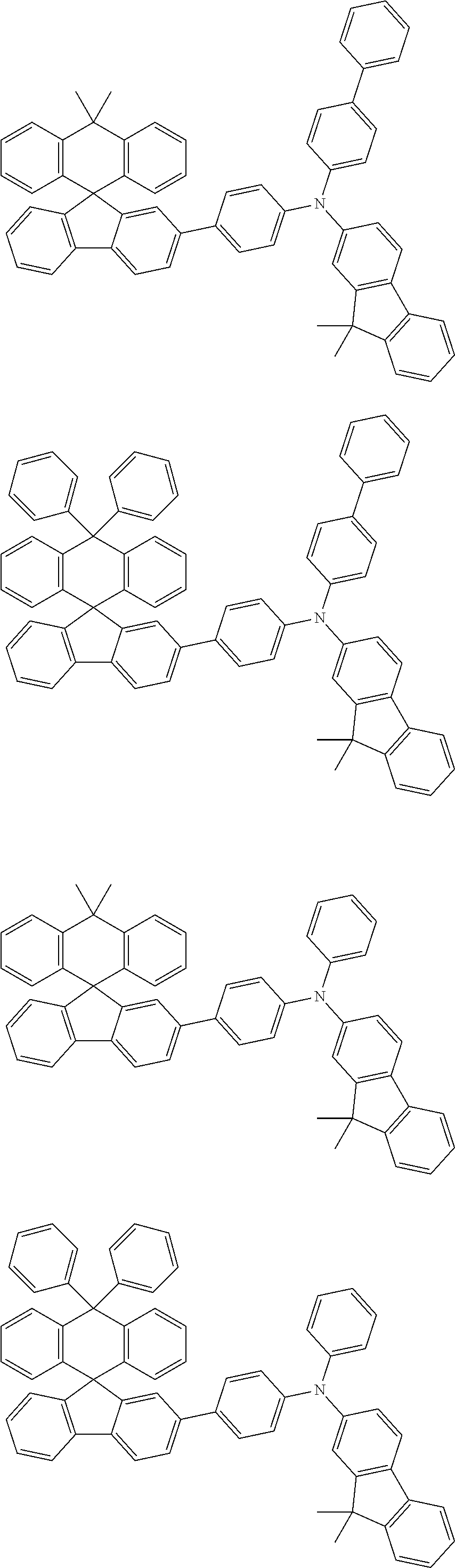


| TABLE 1 | |||||
| Compound | Voltage | Efficiency | |||
| (Electron | (V@10 | (cd/ | Color | ||
| blocking | mA/ | A@10 | coordinate | T95 | |
| layer) | cm2) | mA/cm2) | (x, y) | (hr) | |
| Example 1-1 | Preparation | 4.50 | 6.31 | (0.140, 0.046) | 280 |
| Example 1 | |||||
| Example 1-2 | Preparation | 4.33 | 6.53 | (0.141, 0.046) | 285 |
| Example 3 | |||||
| Example 1-3 | Preparation | 4.56 | 6.34 | (0.143, 0.047) | 295 |
| Example 4 | |||||
| Example 1-4 | Preparation | 4.40 | 6.45 | (0.142, 0.048) | 280 |
| Example 5 | |||||
| Example 1-5 | Preparation | 4.53 | 6.36 | (0.140, 0.044) | 275 |
| Example 6 | |||||
| Example 1-6 | Preparation | 4.56 | 6.37 | (0.141, 0.046) | 285 |
| Example 7 | |||||
| Example 1-7 | Preparation | 4.64 | 6.29 | (0.140, 0.044) | 290 |
| Example 9 | |||||
| Example 1-8 | Preparation | 4.46 | 6.44 | (0.141, 0.046) | 260 |
| Example 10 | |||||
| Example 1-9 | Preparation | 4.41 | 6.42 | (0.138, 0.044) | 280 |
| Example 11 | |||||
| Example 1-10 | Preparation | 4.50 | 6.33 | (0.139, 0.043) | 295 |
| Example 14 | |||||
| Example 1-11 | Preparation | 4.53 | 6.35 | (0.140, 0.047) | 285 |
| Example 15 | |||||
| Example 1-12 | Preparation | 4.56 | 6.31 | (0.141, 0.046) | 270 |
| Example 17 | |||||
| Example 1-13 | Preparation | 4.68 | 6.26 | (0.138, 0.044) | 265 |
| Example 18 | |||||
| Example 1-14 | Preparation | 4.63 | 6.28 | (0.139, 0.043) | 285 |
| Example 19 | |||||
| Example 1-15 | Preparation | 4.62 | 6.23 | (0.142, 0.045) | 275 |
| Example 20 | |||||
| Example 1-16 | Preparation | 4.61 | 6.27 | (0.141, 0.044) | 290 |
| Example 21 | |||||
| Comparative | EB1 | 5.12 | 5.84 | (0.141, 0.045) | 240 |
| Example 1-1 | |||||
| Comparative | EB2 | 4.97 | 5.86 | (0.143, 0.048) | 235 |
| Example 1-2 | |||||
| Comparative | EB3 | 4.72 | 5.43 | (0.143, 0.048) | 220 |
| Example 1-3 | |||||

| TABLE 2 | |||||
| Compound | Voltage | Efficiency | |||
| (Hole | (V@10 | (cd/ | Color | ||
| transport | mA/ | A@10 | coordinate | T95 | |
| layer) | cm2) | mA/cm2) | (x, y) | (hr) | |
| Comparative | HT1 | 5.12 | 5.84 | (0.141, 0.045) | 240 |
| Example 1-1 | |||||
| Example 2-1 | Preparation | 4.50 | 6.31 | (0.140, 0.046) | 280 |
| Example 1 | |||||
| Example 2-2 | Preparation | 4.38 | 6.53 | (0.139, 0.045) | 270 |
| Example 2 | |||||
| Example 2-3 | Preparation | 4.33 | 6.58 | (0.141, 0.046) | 285 |
| Example 3 | |||||
| Example 2-4 | Preparation | 4.56 | 6.34 | (0.143, 0.047) | 295 |
| Example 4 | |||||
| Example 2-5 | Preparation | 4.40 | 6.45 | (0.142, 0.048) | 280 |
| Example 5 | |||||
| Example 2-6 | Preparation | 4.53 | 6.36 | (0.140, 0.044) | 275 |
| Example 6 | |||||
| Example 2-7 | Preparation | 4.56 | 6.37 | (0.141, 0.046) | 285 |
| Example 7 | |||||
| Example 2-8 | Preparation | 4.40 | 6.45 | (0.142, 0.048) | 280 |
| Example 8 | |||||
| Example 2-9 | Preparation | 4.64 | 6.29 | (0.140, 0.044) | 290 |
| Example 9 | |||||
| Example 2-10 | Preparation | 4.46 | 6.44 | (0.141, 0.046) | 260 |
| Example 10 | |||||
| Example 2-11 | Preparation | 4.41 | 6.42 | (0.138, 0.044) | 280 |
| Example 11 | |||||
| Example 2-12 | Preparation | 4.43 | 6.38 | (0.141, 0.046) | 260 |
| Example 12 | |||||
| Example 2-13 | Preparation | 4.51 | 6.35 | (0.140, 0.047) | 285 |
| Example 13 | |||||
| Example 2-14 | Preparation | 4.50 | 6.33 | (0.139, 0.043) | 295 |
| Example 14 | |||||
| Example 2-15 | Preparation | 4.53 | 6.35 | (0.140, 0.047) | 285 |
| Example 15 | |||||
| Example 2-16 | Preparation | 4.61 | 6.29 | (0.140, 0.046) | 265 |
| Example 16 | |||||
| Example 2-17 | Preparation | 4.56 | 6.31 | (0.141, 0.046) | 270 |
| Example 17 | |||||
| Example 2-18 | Preparation | 4.68 | 6.26 | (0.138, 0.044) | 265 |
| Example 18 | |||||
| Example 2-19 | Preparation | 4.63 | 6.28 | (0.139, 0.043) | 285 |
| Example 19 | |||||
| Example 2-20 | Preparation | 4.62 | 6.23 | (0.142, 0.045) | 275 |
| Example 20 | |||||
| Example 2-21 | Preparation | 4.61 | 6.27 | (0.141, 0.044) | 290 |
| Example 21 | |||||
| Example 2-22 | Preparation | 4.58 | 6.31 | (0.139, 0.047) | 270 |
| Example 22 | |||||
| Comparative | HT2 | 5.07 | 5.86 | (0.143, 0.048) | 235 |
| Example 2-1 | |||||
| Comparative | HT3 | 4.92 | 5.43 | (0.143, 0.048) | 220 |
| Example 2-2 | |||||


| TABLE 3 | |||||
| Compound | Voltage | Efficiency | |||
| (Hole | (V@10 | (cd/ | Color | ||
| transport | mA/ | A@10 | coordinate | T98 | |
| layer) | cm2) | mA/cm2) | (x,y) | (hr) | |
| Example 3-1 | Preparation | 3.58 | 145.92 | (0.254, 0.711) | 240 |
| Example 1 | |||||
| Example 3-2 | Preparation | 3.56 | 146.11 | (0.255, 0.712) | 235 |
| Example 2 | |||||
| Example 3-3 | Preparation | 3.62 | 145.25 | (0.256, 0.711) | 235 |
| Example 3 | |||||
| Example 3-4 | Preparation | 3.63 | 145.34 | (0.256, 0.713) | 230 |
| Example 4 | |||||
| Example 3-5 | Preparation | 4.35 | 136.13 | (0.262, 0.705) | 170 |
| Example 5 | |||||
| Example 3-6 | Preparation | 4.36 | 136.39 | (0.264, 0.706) | 165 |
| Example 6 | |||||
| Example 3-7 | Preparation | 4.38 | 135.91 | (0.262, 0.707) | 160 |
| Example 7 | |||||
| Example 3-8 | Preparation | 4.37 | 135.73 | (0.263, 0.705) | 175 |
| Example 8 | |||||
| Example 3-9 | Preparation | 4.12 | 137.97 | (0.261, 0.706) | 170 |
| Example 11 | |||||
| Example 3-10 | Preparation | 4.10 | 138.62 | (0.265, 0.702) | 175 |
| Example 12 | |||||
| Example 3-11 | Preparation | 3.82 | 143.50 | (0.254, 0.711) | 220 |
| Example 14 | |||||
| Example 3-12 | Preparation | 3.86 | 142.44 | (0.255, 0.710) | 215 |
| Example 15 | |||||
| Example 3-13 | Preparation | 4.18 | 138.97 | (0.261, 0.705) | 150 |
| Example 17 | |||||
| Example 3-14 | Preparation | 4.17 | 139.62 | (0.263, 0.708) | 145 |
| Example 18 | |||||
| Example 3-15 | Preparation | 4.35 | 136.13 | (0.266, 0.709) | 180 |
| Example 20 | |||||
| Example 3-16 | Preparation | 4.36 | 136.39 | (0.267, 0.708) | 195 |
| Example 21 | |||||
| Comparative | EB4 | 4.61 | 126.94 | (0.263, 0.704) | 60 |
| Example 3-1 | |||||
| Comparative | EB5 | 4.77 | 125.66 | (0.262, 0.707) | 115 |
| Example 3-2 | |||||
| Comparative | EB6 | 4.52 | 127.43 | (0.261, 0.706) | 85 |
| Example 3-3 | |||||


| TABLE 4 | |||||
| Compound | Voltage | Efficiency | |||
| (Hole | (V@10 | (cd/ | Color | ||
| transport | mA/ | A@10 | coordinate | T98 | |
| layer) | cm2) | mA/cm2) | (x,y) | (hr) | |
| Example 4-1 | Preparation | 4.08 | 47.21 | (0.685, 0.315) | 340 |
| Example 1 | |||||
| Example 4-2 | Preparation | 4.09 | 47.10 | (0.686, 0.314) | 335 |
| Example 2 | |||||
| Example 4-3 | Preparation | 4.04 | 46.55 | (0.685, 0.315) | 335 |
| Example 3 | |||||
| Example 4-4 | Preparation | 4.07 | 45.96 | (0.686, 0.316) | 330 |
| Example 4 | |||||
| Example 4-5 | Preparation | 4.45 | 42.17 | (0.688, 0.318) | 270 |
| Example 5 | |||||
| Example 4-6 | Preparation | 4.49 | 42.39 | (0.689, 0.319) | 265 |
| Example 6 | |||||
| Example 4-7 | Preparation | 4.41 | 42.71 | (0.687, 0.317) | 260 |
| Example 7 | |||||
| Example 4-8 | Preparation | 4.43 | 42.62 | (0.688, 0.321) | 275 |
| Example 8 | |||||
| Example 4-9 | Preparation | 4.32 | 43.83 | (0.687, 0.323) | 270 |
| Example 11 | |||||
| Example 4-10 | Preparation | 4.37 | 43.94 | (0.688, 0.320) | 275 |
| Example 12 | |||||
| Example 4-11 | Preparation | 4.15 | 44.45 | (0.686, 0.316) | 320 |
| Example 14 | |||||
| Example 4-12 | Preparation | 4.13 | 44.70 | (0.686, 0.317) | 315 |
| Example 15 | |||||
| Example 4-13 | Preparation | 4.36 | 43.72 | (0.690, 0.318) | 250 |
| Example 17 | |||||
| Example 4-14 | Preparation | 4.37 | 43.56 | (0.689, 0.319) | 245 |
| Example 18 | |||||
| Example 4-15 | Preparation | 4.01 | 45.64 | (0.690, 0.320) | 280 |
| Example 20 | |||||
| Example 4-16 | Preparation | 4.05 | 45.61 | (0.685, 0.315) | 295 |
| Example 21 | |||||
| Comparative | HT5 | 5.32 | 38.69 | (0.692, 0.324) | 145 |
| Example 4-1 | |||||
| Comparative | HT6 | 4.87 | 45.63 | (0.687, 0.319) | 190 |
| Example 4-2 | |||||
| Comparative | HT7 | 5.13 | 41.05 | (0.693, 0.323) | 160 |
| Example 4-3 | |||||
| Description of symbols |
| 1: | substrate |
| 2: | anode |
| 3: | organic material layer |
| 4: | cathode |
| 5: | hole injection layer |
| 6: | hole transport layer |
| 7: | electron blocking layer |
| 8: | light emitting layer |
| 9: | electron transport layer |
| 10: | electron injection layer |
Claims (10)


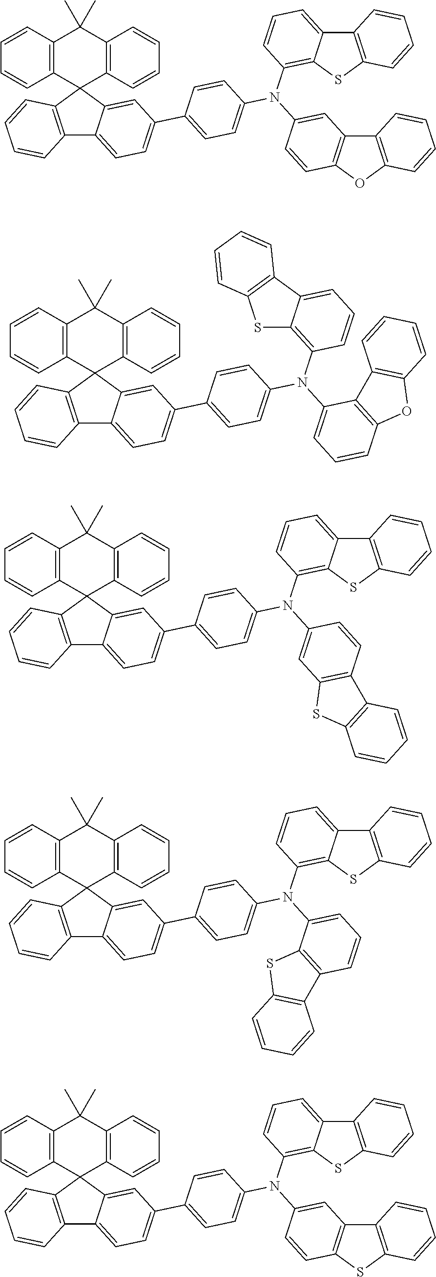


Applications Claiming Priority (5)
| Application Number | Priority Date | Filing Date | Title |
|---|---|---|---|
| KR20170063091 | 2017-05-22 | ||
| KR10-2017-0063091 | 2017-05-22 | ||
| KR10-2018-0002356 | 2018-01-08 | ||
| KR1020180002356A KR102080288B1 (en) | 2017-05-22 | 2018-01-08 | Novel compound and organic light emitting device comprising the same |
| PCT/KR2018/004249 WO2018216903A1 (en) | 2017-05-22 | 2018-04-11 | Novel compound and organic light-emitting device using same |
Publications (2)
| Publication Number | Publication Date |
|---|---|
| US20200131112A1 US20200131112A1 (en) | 2020-04-30 |
| US11459290B2 true US11459290B2 (en) | 2022-10-04 |
Family
ID=64560823
Family Applications (1)
| Application Number | Title | Priority Date | Filing Date |
|---|---|---|---|
| US16/487,404 Active 2039-02-12 US11459290B2 (en) | 2017-05-22 | 2018-04-11 | Compound and organic light emitting device using the same |
Country Status (6)
| Country | Link |
|---|---|
| US (1) | US11459290B2 (en) |
| EP (1) | EP3567026B1 (en) |
| JP (1) | JP6818998B2 (en) |
| KR (1) | KR102080288B1 (en) |
| CN (1) | CN110382457B (en) |
| TW (1) | TWI658030B (en) |
Families Citing this family (8)
| Publication number | Priority date | Publication date | Assignee | Title |
|---|---|---|---|---|
| KR102220220B1 (en) * | 2017-06-14 | 2021-02-24 | 솔루스첨단소재 주식회사 | Organic compounds and organic electro luminescence device comprising the same |
| CN109705018B (en) * | 2017-12-27 | 2022-10-04 | 广州华睿光电材料有限公司 | Organic compound, organic mixture, composition and organic electronic device |
| KR20190120538A (en) * | 2018-04-16 | 2019-10-24 | 주식회사 두산 | Organic light-emitting compound and organic electroluminescent device using the same |
| CN115785063A (en) * | 2018-09-17 | 2023-03-14 | 北京鼎材科技有限公司 | Organic compound and organic electroluminescent device |
| KR102475856B1 (en) * | 2019-02-15 | 2022-12-08 | 주식회사 엘지화학 | Novel compound and organic light emitting device comprising the same |
| CN112745229B (en) * | 2019-10-31 | 2023-12-05 | 南京高光半导体材料有限公司 | Hole transport material with excellent performance and organic electroluminescent device containing same |
| CN110885321A (en) * | 2019-11-25 | 2020-03-17 | 武汉华星光电半导体显示技术有限公司 | Hole transport material, preparation method thereof and electroluminescent device |
| CN112239411B (en) | 2019-12-30 | 2021-11-12 | 陕西莱特光电材料股份有限公司 | Nitrogen-containing compound, electronic component, and electronic device |
Citations (18)
| Publication number | Priority date | Publication date | Assignee | Title |
|---|---|---|---|---|
| KR0169570B1 (en) | 1996-02-03 | 1999-01-15 | 챠노 다까시 | Fluid pump |
| KR20000051826A (en) | 1999-01-27 | 2000-08-16 | 성재갑 | New organomattalic complex molecule for the fabrication of organic light emitting diodes |
| WO2003012890A2 (en) | 2001-07-20 | 2003-02-13 | Novaled Gmbh | Light emitting component with organic layers |
| US20030168970A1 (en) * | 2000-11-24 | 2003-09-11 | Tsuyoshi Tominaga | Luminescent element material and luminescent element comprising the same |
| US7507485B2 (en) * | 2001-10-30 | 2009-03-24 | Lg Display Co., Ltd. | Organic electroluminescent device |
| JP2009191232A (en) | 2008-02-18 | 2009-08-27 | Toppan Printing Co Ltd | Fluorescent compound, light-emitting ink composition and organic el device |
| KR20130140303A (en) | 2012-06-14 | 2013-12-24 | (주) 에프엔지리서치 | Novel compounds for organic electroluminescent device |
| KR20150083917A (en) | 2012-11-12 | 2015-07-20 | 메르크 파텐트 게엠베하 | Materials for electronic devices |
| KR20160102949A (en) | 2016-08-22 | 2016-08-31 | (주) 에프엔지리서치 | Novel compounds for organic electroluminescent device |
| KR20160131887A (en) | 2015-05-08 | 2016-11-16 | 머티어리얼사이언스 주식회사 | Organic electroluminescent device |
| WO2016182270A1 (en) | 2015-05-08 | 2016-11-17 | 머티어리얼사이언스 주식회사 | Organic electroluminescent device |
| TWI560171B (en) | 2015-10-16 | 2016-12-01 | Tetrahedron Technology Corp | Organic electroluminescent devices and material thereof |
| US20160351817A1 (en) | 2015-05-27 | 2016-12-01 | Samsung Display Co., Ltd. | Organic light-emitting device |
| KR20160141361A (en) | 2015-05-27 | 2016-12-08 | 삼성디스플레이 주식회사 | Organic light-emitting device |
| KR101695270B1 (en) | 2015-11-17 | 2017-01-12 | 머티어리얼사이언스 주식회사 | Spyro-typed organic materials and organic electroluminescent device utilizing the same |
| JP2017502007A (en) | 2013-12-12 | 2017-01-19 | メルク パテント ゲーエムベーハー | Materials for electronic devices |
| WO2018164265A1 (en) | 2017-03-10 | 2018-09-13 | 出光興産株式会社 | Compound, organic electroluminescent element material, organic electroluminescent element, and electronic device |
| KR20180136218A (en) | 2017-06-14 | 2018-12-24 | 주식회사 두산 | Organic compounds and organic electro luminescence device comprising the same |
-
2018
- 2018-01-08 KR KR1020180002356A patent/KR102080288B1/en active IP Right Grant
- 2018-04-11 CN CN201880012821.3A patent/CN110382457B/en active Active
- 2018-04-11 US US16/487,404 patent/US11459290B2/en active Active
- 2018-04-11 EP EP18805701.2A patent/EP3567026B1/en active Active
- 2018-04-11 JP JP2019546159A patent/JP6818998B2/en active Active
- 2018-04-19 TW TW107113268A patent/TWI658030B/en active
Patent Citations (25)
| Publication number | Priority date | Publication date | Assignee | Title |
|---|---|---|---|---|
| KR0169570B1 (en) | 1996-02-03 | 1999-01-15 | 챠노 다까시 | Fluid pump |
| KR20000051826A (en) | 1999-01-27 | 2000-08-16 | 성재갑 | New organomattalic complex molecule for the fabrication of organic light emitting diodes |
| US20030168970A1 (en) * | 2000-11-24 | 2003-09-11 | Tsuyoshi Tominaga | Luminescent element material and luminescent element comprising the same |
| WO2003012890A2 (en) | 2001-07-20 | 2003-02-13 | Novaled Gmbh | Light emitting component with organic layers |
| US7507485B2 (en) * | 2001-10-30 | 2009-03-24 | Lg Display Co., Ltd. | Organic electroluminescent device |
| JP2009191232A (en) | 2008-02-18 | 2009-08-27 | Toppan Printing Co Ltd | Fluorescent compound, light-emitting ink composition and organic el device |
| KR20130140303A (en) | 2012-06-14 | 2013-12-24 | (주) 에프엔지리서치 | Novel compounds for organic electroluminescent device |
| KR20150083917A (en) | 2012-11-12 | 2015-07-20 | 메르크 파텐트 게엠베하 | Materials for electronic devices |
| US20150295181A1 (en) | 2012-11-12 | 2015-10-15 | Merck Patent Gmbh | Materials for electronic devices |
| JP2017502007A (en) | 2013-12-12 | 2017-01-19 | メルク パテント ゲーエムベーハー | Materials for electronic devices |
| US10158083B2 (en) | 2013-12-12 | 2018-12-18 | Merck Patent Gmbh | Materials for electronic devices |
| CN106612616A (en) | 2015-05-08 | 2017-05-03 | 陕西莱特迈思光电材料有限公司 | Organic electroluminescent device |
| KR20160131887A (en) | 2015-05-08 | 2016-11-16 | 머티어리얼사이언스 주식회사 | Organic electroluminescent device |
| WO2016182270A1 (en) | 2015-05-08 | 2016-11-17 | 머티어리얼사이언스 주식회사 | Organic electroluminescent device |
| US20160351817A1 (en) | 2015-05-27 | 2016-12-01 | Samsung Display Co., Ltd. | Organic light-emitting device |
| KR20160141361A (en) | 2015-05-27 | 2016-12-08 | 삼성디스플레이 주식회사 | Organic light-emitting device |
| TWI560171B (en) | 2015-10-16 | 2016-12-01 | Tetrahedron Technology Corp | Organic electroluminescent devices and material thereof |
| CN106588674A (en) | 2015-10-16 | 2017-04-26 | 晶宜科技股份有限公司 | Organic electroluminescent device and material thereof |
| KR101695270B1 (en) | 2015-11-17 | 2017-01-12 | 머티어리얼사이언스 주식회사 | Spyro-typed organic materials and organic electroluminescent device utilizing the same |
| KR20160102949A (en) | 2016-08-22 | 2016-08-31 | (주) 에프엔지리서치 | Novel compounds for organic electroluminescent device |
| WO2018164265A1 (en) | 2017-03-10 | 2018-09-13 | 出光興産株式会社 | Compound, organic electroluminescent element material, organic electroluminescent element, and electronic device |
| JP2020097525A (en) | 2017-03-10 | 2020-06-25 | 出光興産株式会社 | Compound, material for organic electroluminescence element, organic electroluminescence element, and electronic apparatus |
| KR20180136218A (en) | 2017-06-14 | 2018-12-24 | 주식회사 두산 | Organic compounds and organic electro luminescence device comprising the same |
| CN110785401A (en) | 2017-06-14 | 2020-02-11 | 株式会社斗山 | Organic compound and organic electroluminescent element comprising same |
| US20210147336A1 (en) | 2017-06-14 | 2021-05-20 | Doosan Solus Co., Ltd. | Organic compound and organic electroluminescent device comprising same |
Non-Patent Citations (6)
| Title |
|---|
| Chem. Rev. (2007), vol. 107, pp. 1011-1065. (Year: 2007). * |
| International Search Report from PCT/KR2018/004249, dated Aug. 10, 2018. |
| Machine translation for CN 106588674 A (publication date: Apr. 2017). (Year: 2017). * |
| Notice of Allowance of Japanese Patent Office in Appl'n No. 2019-546159, dated Dec. 1, 2020. |
| Office Action of Chinese Patent Office in Appl'n No. 201880012821.3, dated Dec. 8, 2021. |
| Written Opinion of the ISA from PCT/KR2018/004249, dated Aug. 10, 2018. |
Also Published As
| Publication number | Publication date |
|---|---|
| KR20180127900A (en) | 2018-11-30 |
| KR102080288B1 (en) | 2020-02-21 |
| JP2020510652A (en) | 2020-04-09 |
| EP3567026A4 (en) | 2020-01-29 |
| US20200131112A1 (en) | 2020-04-30 |
| CN110382457A (en) | 2019-10-25 |
| TW201900600A (en) | 2019-01-01 |
| EP3567026B1 (en) | 2021-12-29 |
| TWI658030B (en) | 2019-05-01 |
| CN110382457B (en) | 2022-06-14 |
| EP3567026A1 (en) | 2019-11-13 |
| JP6818998B2 (en) | 2021-01-27 |
Similar Documents
| Publication | Publication Date | Title |
|---|---|---|
| US11802123B2 (en) | Heterocyclic compound and organic light emitting device comprising the same | |
| US11459290B2 (en) | Compound and organic light emitting device using the same | |
| US11081655B2 (en) | Heterocyclic compound and organic light emitting device using the same | |
| US20220017544A1 (en) | Novel compound and organic light emitting device comprising the same | |
| US20220352472A1 (en) | Cyclic compound and organic light emitting device comprising same | |
| US20210130295A1 (en) | Compound and organic light emitting device comprising the same | |
| US20210363132A1 (en) | Novel compound and organic light emitting device comprising the same | |
| US11621397B2 (en) | Iridium complexes containing a ligand including a (dibenzo [B,D] furanyl) pyridine skeleton having deuterium substitutions para and meta to the N ring atom and organic light emitting device comprising the same | |
| US11515478B2 (en) | Compound and organic light emitting device using the same | |
| US20190312223A1 (en) | Organic light emitting device | |
| US11228001B2 (en) | Hetero-cyclic compound and organic light emitting device comprising the same | |
| US20200106017A1 (en) | Novel compound and organic light emitting device using the same | |
| US11407718B2 (en) | Heterocyclic compound and organic light emitting device comprising the same | |
| US20220085300A1 (en) | Organic light emitting device | |
| US11404654B2 (en) | Compound containing iridium complex with aza dibenzo group and organic light emitting device comprising same | |
| US11700768B2 (en) | Compound and organic light emitting device comprising the same | |
| US20210296593A1 (en) | Novel compound and organic light emitting device comprising the same | |
| US11453650B2 (en) | Heterocyclic compound and organic light emitting device comprising the same | |
| US20210280794A1 (en) | Novel compound and organic light emitting device comprising the same | |
| US20200287143A1 (en) | Organometallic compound and organic light emitting device comprising same | |
| US11261176B2 (en) | Amine-based compound and organic light emitting device using the same | |
| US20220302392A1 (en) | Organic light emitting device | |
| US11778909B2 (en) | Compound and organic light emitting device comprising the same | |
| US11926607B2 (en) | Compound and organic light emitting device comprising the same | |
| US11746117B2 (en) | Heterocyclic compound and organic light emitting device comprising same |
Legal Events
| Date | Code | Title | Description |
|---|---|---|---|
| AS | Assignment |
Owner name: LG CHEM, LTD., KOREA, REPUBLIC OF Free format text: ASSIGNMENT OF ASSIGNORS INTEREST;ASSIGNORS:CHA, YONG BUM;LEE, SUNG JAE;KIM, YEON HWAN;AND OTHERS;REEL/FRAME:050108/0489 Effective date: 20190515 |
|
| FEPP | Fee payment procedure |
Free format text: ENTITY STATUS SET TO UNDISCOUNTED (ORIGINAL EVENT CODE: BIG.); ENTITY STATUS OF PATENT OWNER: LARGE ENTITY |
|
| STPP | Information on status: patent application and granting procedure in general |
Free format text: DOCKETED NEW CASE - READY FOR EXAMINATION |
|
| STPP | Information on status: patent application and granting procedure in general |
Free format text: NON FINAL ACTION MAILED |
|
| STPP | Information on status: patent application and granting procedure in general |
Free format text: RESPONSE TO NON-FINAL OFFICE ACTION ENTERED AND FORWARDED TO EXAMINER |
|
| STPP | Information on status: patent application and granting procedure in general |
Free format text: FINAL REJECTION MAILED |
|
| STPP | Information on status: patent application and granting procedure in general |
Free format text: ADVISORY ACTION MAILED |
|
| STPP | Information on status: patent application and granting procedure in general |
Free format text: NOTICE OF ALLOWANCE MAILED -- APPLICATION RECEIVED IN OFFICE OF PUBLICATIONS |
|
| STPP | Information on status: patent application and granting procedure in general |
Free format text: PUBLICATIONS -- ISSUE FEE PAYMENT VERIFIED |
|
| STCF | Information on status: patent grant |
Free format text: PATENTED CASE |