US11746117B2 - Heterocyclic compound and organic light emitting device comprising same - Google Patents

Heterocyclic compound and organic light emitting device comprising same Download PDF

Info

Publication number
US11746117B2
US11746117B2 US17/275,664 US201917275664A US11746117B2 US 11746117 B2 US11746117 B2 US 11746117B2 US 201917275664 A US201917275664 A US 201917275664A US 11746117 B2 US11746117 B2 US 11746117B2
Authority
US
United States
Prior art keywords
group
compound
layer
light emitting
substituted
Prior art date
Legal status (The legal status is an assumption and is not a legal conclusion. Google has not performed a legal analysis and makes no representation as to the accuracy of the status listed.)
Active, expires
Application number
US17/275,664
Other versions
US20220056047A1 (en
Inventor
Min Woo JUNG
Dong Hoon Lee
Boon Jae JANG
Wanpyo HONG
Sang Duk Suh
Jungha Lee
Su Jin HAN
Seulchan PARK
Sunghyun Hwang
Current Assignee (The listed assignees may be inaccurate. Google has not performed a legal analysis and makes no representation or warranty as to the accuracy of the list.)
LG Chem Ltd
Original Assignee
LG Chem Ltd
Priority date (The priority date is an assumption and is not a legal conclusion. Google has not performed a legal analysis and makes no representation as to the accuracy of the date listed.)
Filing date
Publication date
Priority claimed from KR1020190145261A external-priority patent/KR102265929B1/en
Application filed by LG Chem Ltd filed Critical LG Chem Ltd
Assigned to LG CHEM, LTD. reassignment LG CHEM, LTD. ASSIGNMENT OF ASSIGNORS INTEREST (SEE DOCUMENT FOR DETAILS). Assignors: HONG, Wanpyo, LEE, JUNGHA, SUH, SANG DUK, HAN, SU JIN, HWANG, SUNGHYUN, JANG, BOON JAE, JUNG, MIN WOO, LEE, DONG HOON, PARK, Seulchan
Publication of US20220056047A1 publication Critical patent/US20220056047A1/en
Application granted granted Critical
Publication of US11746117B2 publication Critical patent/US11746117B2/en
Active legal-status Critical Current
Adjusted expiration legal-status Critical

Links

Images

Classifications

    • CCHEMISTRY; METALLURGY
    • C07ORGANIC CHEMISTRY
    • C07DHETEROCYCLIC COMPOUNDS
    • C07D519/00Heterocyclic compounds containing more than one system of two or more relevant hetero rings condensed among themselves or condensed with a common carbocyclic ring system not provided for in groups C07D453/00 or C07D455/00
    • CCHEMISTRY; METALLURGY
    • C07ORGANIC CHEMISTRY
    • C07DHETEROCYCLIC COMPOUNDS
    • C07D403/00Heterocyclic compounds containing two or more hetero rings, having nitrogen atoms as the only ring hetero atoms, not provided for by group C07D401/00
    • C07D403/14Heterocyclic compounds containing two or more hetero rings, having nitrogen atoms as the only ring hetero atoms, not provided for by group C07D401/00 containing three or more hetero rings
    • CCHEMISTRY; METALLURGY
    • C07ORGANIC CHEMISTRY
    • C07DHETEROCYCLIC COMPOUNDS
    • C07D407/00Heterocyclic compounds containing two or more hetero rings, at least one ring having oxygen atoms as the only ring hetero atoms, not provided for by group C07D405/00
    • C07D407/14Heterocyclic compounds containing two or more hetero rings, at least one ring having oxygen atoms as the only ring hetero atoms, not provided for by group C07D405/00 containing three or more hetero rings
    • CCHEMISTRY; METALLURGY
    • C07ORGANIC CHEMISTRY
    • C07DHETEROCYCLIC COMPOUNDS
    • C07D409/00Heterocyclic compounds containing two or more hetero rings, at least one ring having sulfur atoms as the only ring hetero atoms
    • C07D409/14Heterocyclic compounds containing two or more hetero rings, at least one ring having sulfur atoms as the only ring hetero atoms containing three or more hetero rings
    • CCHEMISTRY; METALLURGY
    • C07ORGANIC CHEMISTRY
    • C07DHETEROCYCLIC COMPOUNDS
    • C07D413/00Heterocyclic compounds containing two or more hetero rings, at least one ring having nitrogen and oxygen atoms as the only ring hetero atoms
    • C07D413/14Heterocyclic compounds containing two or more hetero rings, at least one ring having nitrogen and oxygen atoms as the only ring hetero atoms containing three or more hetero rings
    • CCHEMISTRY; METALLURGY
    • C07ORGANIC CHEMISTRY
    • C07DHETEROCYCLIC COMPOUNDS
    • C07D417/00Heterocyclic compounds containing two or more hetero rings, at least one ring having nitrogen and sulfur atoms as the only ring hetero atoms, not provided for by group C07D415/00
    • C07D417/14Heterocyclic compounds containing two or more hetero rings, at least one ring having nitrogen and sulfur atoms as the only ring hetero atoms, not provided for by group C07D415/00 containing three or more hetero rings
    • CCHEMISTRY; METALLURGY
    • C07ORGANIC CHEMISTRY
    • C07DHETEROCYCLIC COMPOUNDS
    • C07D498/00Heterocyclic compounds containing in the condensed system at least one hetero ring having nitrogen and oxygen atoms as the only ring hetero atoms
    • C07D498/02Heterocyclic compounds containing in the condensed system at least one hetero ring having nitrogen and oxygen atoms as the only ring hetero atoms in which the condensed system contains two hetero rings
    • C07D498/04Ortho-condensed systems
    • CCHEMISTRY; METALLURGY
    • C07ORGANIC CHEMISTRY
    • C07DHETEROCYCLIC COMPOUNDS
    • C07D513/00Heterocyclic compounds containing in the condensed system at least one hetero ring having nitrogen and sulfur atoms as the only ring hetero atoms, not provided for in groups C07D463/00, C07D477/00 or C07D499/00 - C07D507/00
    • C07D513/02Heterocyclic compounds containing in the condensed system at least one hetero ring having nitrogen and sulfur atoms as the only ring hetero atoms, not provided for in groups C07D463/00, C07D477/00 or C07D499/00 - C07D507/00 in which the condensed system contains two hetero rings
    • C07D513/04Ortho-condensed systems
    • HELECTRICITY
    • H10SEMICONDUCTOR DEVICES; ELECTRIC SOLID-STATE DEVICES NOT OTHERWISE PROVIDED FOR
    • H10KORGANIC ELECTRIC SOLID-STATE DEVICES
    • H10K85/00Organic materials used in the body or electrodes of devices covered by this subclass
    • H10K85/60Organic compounds having low molecular weight
    • H10K85/649Aromatic compounds comprising a hetero atom
    • H10K85/654Aromatic compounds comprising a hetero atom comprising only nitrogen as heteroatom
    • HELECTRICITY
    • H10SEMICONDUCTOR DEVICES; ELECTRIC SOLID-STATE DEVICES NOT OTHERWISE PROVIDED FOR
    • H10KORGANIC ELECTRIC SOLID-STATE DEVICES
    • H10K85/00Organic materials used in the body or electrodes of devices covered by this subclass
    • H10K85/60Organic compounds having low molecular weight
    • H10K85/649Aromatic compounds comprising a hetero atom
    • H10K85/657Polycyclic condensed heteroaromatic hydrocarbons
    • H10K85/6572Polycyclic condensed heteroaromatic hydrocarbons comprising only nitrogen in the heteroaromatic polycondensed ring system, e.g. phenanthroline or carbazole
    • HELECTRICITY
    • H10SEMICONDUCTOR DEVICES; ELECTRIC SOLID-STATE DEVICES NOT OTHERWISE PROVIDED FOR
    • H10KORGANIC ELECTRIC SOLID-STATE DEVICES
    • H10K85/00Organic materials used in the body or electrodes of devices covered by this subclass
    • H10K85/60Organic compounds having low molecular weight
    • H10K85/649Aromatic compounds comprising a hetero atom
    • H10K85/657Polycyclic condensed heteroaromatic hydrocarbons
    • H10K85/6574Polycyclic condensed heteroaromatic hydrocarbons comprising only oxygen in the heteroaromatic polycondensed ring system, e.g. cumarine dyes
    • HELECTRICITY
    • H10SEMICONDUCTOR DEVICES; ELECTRIC SOLID-STATE DEVICES NOT OTHERWISE PROVIDED FOR
    • H10KORGANIC ELECTRIC SOLID-STATE DEVICES
    • H10K2101/00Properties of the organic materials covered by group H10K85/00
    • H10K2101/10Triplet emission
    • HELECTRICITY
    • H10SEMICONDUCTOR DEVICES; ELECTRIC SOLID-STATE DEVICES NOT OTHERWISE PROVIDED FOR
    • H10KORGANIC ELECTRIC SOLID-STATE DEVICES
    • H10K2101/00Properties of the organic materials covered by group H10K85/00
    • H10K2101/30Highest occupied molecular orbital [HOMO], lowest unoccupied molecular orbital [LUMO] or Fermi energy values
    • HELECTRICITY
    • H10SEMICONDUCTOR DEVICES; ELECTRIC SOLID-STATE DEVICES NOT OTHERWISE PROVIDED FOR
    • H10KORGANIC ELECTRIC SOLID-STATE DEVICES
    • H10K2101/00Properties of the organic materials covered by group H10K85/00
    • H10K2101/40Interrelation of parameters between multiple constituent active layers or sublayers, e.g. HOMO values in adjacent layers
    • HELECTRICITY
    • H10SEMICONDUCTOR DEVICES; ELECTRIC SOLID-STATE DEVICES NOT OTHERWISE PROVIDED FOR
    • H10KORGANIC ELECTRIC SOLID-STATE DEVICES
    • H10K50/00Organic light-emitting devices
    • H10K50/10OLEDs or polymer light-emitting diodes [PLED]
    • H10K50/11OLEDs or polymer light-emitting diodes [PLED] characterised by the electroluminescent [EL] layers

Definitions

  • the present disclosure relates to a novel compound and an organic light emitting device including the same.
  • an organic light emitting phenomenon refers to a phenomenon where electrical energy is converted into light energy by using an organic material.
  • the organic light emitting device using the organic light emitting phenomenon has characteristics such as a wide viewing angle, an excellent contrast, a fast response time, an excellent luminance, driving voltage and response speed, and thus many studies have proceeded thereon.
  • the organic light emitting device generally has a structure which includes an anode, a cathode, and an organic material layer interposed between the anode and the cathode.
  • the organic material layer frequently has a multilayered structure that includes different materials in order to enhance efficiency and stability of the organic light emitting device, and for example, the organic material layer may be formed of a hole injection layer, a hole transport layer, a light emitting layer, an electron transport layer, an electron injection layer, and the like.
  • the organic light emitting device In the structure of the organic light emitting device, if a voltage is applied between two electrodes, holes are injected from an anode into the organic material layer and electrons are injected from the cathode into the organic material layer, and when the injected holes and electrons meet each other, an exciton is formed, and light is emitted when the exciton falls to a ground state again.
  • Patent Literature 1 Korean Patent Laid-open Publication No. 10-2000-0051826
  • One aspect of the present disclosure provides a compound represented by the following Chemical Formula 1 or 2:
  • X 1 to X 3 are each independently, CH or N, and at least one of X 1 to X 3 is N,
  • Ar 1 and Ar 2 are each independently a substituted or unsubstituted C 6-60 aryl; or a substituted or unsubstituted C 2-60 heteroaryl containing at least one heteroatom selected from the group consisting of N, O, and S,
  • R 1 is each independently deuterium; a substituted or unsubstituted C 6-60 aryl; or a substituted or unsubstituted C 2-60 heteroaryl containing at least one heteroatom selected from the group consisting of N, O, and S,
  • n is an integer of 0 to 8
  • E is a substituent represented by the following Chemical Formula 3-1 or 3-2,
  • X 4 and X 5 are each independently, CH or N, and at least one of X 4 and X 5 is N,
  • Ar 3 is a substituted or unsubstituted C 6-60 aryl; or a substituted or unsubstituted C 2-60 heteroaryl containing at least one heteroatom selected from the group consisting of N, O, and S,
  • A is represented by the following Chemical Formula 4-1 or 4-2,
  • Y is O, S, C(R′) 2 , or NR′,
  • R′ is each independently hydrogen; deuterium; a substituted or unsubstituted C 6-60 aryl; or a substituted or unsubstituted C 2-60 heteroaryl containing at least one heteroatom selected from the group consisting of N, O, and S.
  • an organic light emitting device including a first electrode; a second electrode provided to face the first electrode; and one or more organic material layers provided between the first electrode and the second electrode, wherein one or more layers of the organic material layers include the compound represented by Chemical Formula 1 or 2.
  • the compound represented by Chemical Formula 1 or 2 described above can be used as a material of an organic material layer of an organic light emitting device and may improve the efficiency and achieve a low driving voltage and/or improve lifetime characteristics in the organic light emitting device.
  • the compound represented by Chemical Formula 1 or 2 may be used as a hole injection material, a hole transport material, a hole injection and transport material, a light emitting material, an electron transport material, or an electron injection material.
  • FIG. 1 depicts an example of an organic light emitting device including a substrate 1 , an anode 2 , a organic material layer 3 , and a cathode 4 .
  • FIG. 2 depicts an example of an organic light emitting device including a substrate 1 , an anode 2 , a hole injection layer 5 , a hole transport layer 6 , an electron blocking layer 7 , a light emitting layer 8 , a hole blocking layer 9 , an electron transport layer 10 , an electron injection layer 11 , and a cathode 4 .
  • One embodiment of the disclosure provides a compound represented by Chemical Formula 1 or 2.
  • substituted or unsubstituted means that substitution is performed by one or more substituent groups selected from the group consisting of deuterium; a halogen group; a nitrile group; a nitro group; a hydroxyl group; a carbonyl group; an ester group; an imide group; an amino group; a phosphine oxide group; an alkoxy group; an aryloxy group; an alkylthioxy group; an arylthioxy group; an alkylsulfoxy group; an arylsulfoxy group; a silyl group; a boron group; an alkyl group; a cycloalkyl group; an alkenyl group; an aryl group; an aralkyl group; an aralkenyl group; an alkylaryl group; an alkylamine group; an aralkylamine group; a heteroarylamine group; an arylamine group; an arylphosphine oxide group; an alkoxy group
  • substituted group where two or more substituent groups are linked may be a biphenyl group. That is, the biphenyl group may be an aryl group, or may be interpreted as a substituent group where two phenyl groups are connected.
  • the number of carbon atoms in a carbonyl group is not particularly limited, but is preferably 1 to 40 carbon atoms.
  • the carbonyl group may be compounds having the following structures, but is not limited thereto.
  • the ester group may have a structure in which oxygen of the ester group may be substituted by a straight-chain, branched-chain, or cyclic alkyl group having 1 to 25 carbon atoms, or an aryl group having 6 to 25 carbon atoms.
  • the ester group may be compounds having the following structures, but is not limited thereto.
  • the number of carbon atoms in an imide group is not particularly limited, but is preferably 1 to 25.
  • the imide group may be compounds having the following structures, but is not limited thereto.
  • the silyl group specifically includes a trimethylsilyl group, a triethylsilyl group, a t-butyldimethylsilyl group, a vinyldimethylsilyl group, a propyldimethylsilyl group, a triphenylsilyl group, a diphenylsilyl group, a phenylsilyl group, and the like, but is not limited thereto.
  • the boron group specifically includes a trimethylboron group, a triethylboron group, a t-butyldimethylboron group, a triphenylboron group, a phenylboron group, and the like, but is not limited thereto.
  • examples of a halogen group include fluorine, chlorine, bromine, or iodine.
  • an alkyl group may be a straight chain or a branched chain, and the number of carbon atoms thereof is not particularly limited, but is preferably 1 to 40. According to one embodiment, the alkyl group has 1 to 20 carbon atoms. According to another embodiment, the alkyl group has 1 to 10 carbon atoms. According to still another embodiment, the alkyl group has 1 to 6 carbon atoms.
  • alkyl group examples include methyl, ethyl, propyl, n-propyl, isopropyl, butyl, n-butyl, isobutyl, tert-butyl, sec-butyl, 1-methyl-butyl, 1-ethyl-butyl, pentyl, n-pentyl, isopentyl, neopentyl, tert-pentyl, hexyl, n-hexyl, 1-methylpentyl, 2-methylpentyl, 4-methyl-2-pentyl, 3,3-dimethylbutyl, 2-ethylbutyl, heptyl, n-heptyl, 1-methylhexyl, cyclopentylmethyl, cyclohexylmethyl, octyl, n-octyl, tert-octyl, 1-methylheptyl, 2-ethylhexyl, 2-
  • the alkenyl group may be a straight chain or a branched chain, and the number of carbon atoms thereof is not particularly limited, but is preferably 2 to 40. According to one embodiment, the alkenyl group has 2 to 20 carbon atoms. According to another embodiment, the alkenyl group has 2 to 10 carbon atoms. According to still another embodiment, the alkenyl group has 2 to 6 carbon atoms.
  • Specific examples thereof include vinyl, 1-propenyl, isopropenyl, 1-butenyl, 2-butenyl, 3-butenyl, 1-pentenyl, 2-pentenyl, 3-pentenyl, 3-methyl-1-butenyl, 1,3-butadienyl, allyl, 1-phenylvinyl-1-yl, 2-phenylvinyl-1-yl, 2,2-diphenylvinyl-1-yl, 2-phenyl-2-(naphthyl-1-yl)vinyl-1-yl, 2,2-bis(diphenyl-1-yl)vinyl-1-yl, a stilbenyl group, a styrenyl group, and the like, but are not limited thereto.
  • a cycloalkyl group is not particularly limited, but the number of carbon atoms thereof is preferably 3 to 60. According to one embodiment, the cycloalkyl group has 3 to 30 carbon atoms. According to another embodiment, the cycloalkyl group has 3 to 20 carbon atoms. According to still another embodiment, the cycloalkyl group has 3 to 6 carbon atoms.
  • cyclopropyl examples thereof include cyclopropyl, cyclobutyl, cyclopentyl, 3-methylcyclopentyl, 2,3-dimethylcyclopentyl, cyclohexyl, 3-methylcyclohexyl, 4-methylcyclohexyl, 2,3-dimethylcyclohexyl, 3,4,5-trimethylcyclohexyl, 4-tert-butylcyclohexyl, cycloheptyl, cyclooctyl, and the like, but are not limited thereto.
  • the aryl group is not particularly limited, but preferably has 6 to 60 carbon atoms, and may be a monocyclic aryl group or a polycyclic aryl group. According to one embodiment, the aryl group has 6 to 30 carbon atoms. According to one embodiment, the aryl group has 6 to 20 carbon atoms.
  • the aryl group may be a phenyl group, a biphenyl group, a terphenyl group or the like as the monocyclic aryl group, but is not limited thereto.
  • polycyclic aryl group examples include a naphthyl group, an anthracenyl group, a phenanthryl group, a pyrenyl group, a perylenyl group, a chrycenyl group, a fluorenyl group or the like, but is not limited thereto.
  • a fluorenyl group may be substituted, and two substituent groups may be linked with each other to form a spiro structure.
  • the fluorenyl group is substituted,
  • the heterocyclic group is a heterocyclic group containing at least one of O, N, Si and S as a heteroatom, and the number of carbon atoms thereof is not particularly limited, but is preferably 2 to 60.
  • the heterocyclic group include a thiophene group, a furan group, a pyrrole group, an imidazole group, a thiazole group, an oxazole group, an oxadiazole group, a triazole group, a pyridyl group, a bipyridyl group, a pyrimidyl group, a triazine group, a triazole group, an acridyl group, a pyridazine group, a pyrazinyl group, a quinolinyl group, a quinazoline group, a quinoxalinyl group, a phthalazinyl group, a pyridopyrimidinyl group,
  • the aryl group in the aralkyl group, the aralkenyl group, the alkylaryl group, and the arylamine group is the same as the aforementioned examples of the aryl group.
  • the alkyl group in the aralkyl group, the alkylaryl group and the alkylamine group is the same as the aforementioned examples of the alkyl group.
  • the heteroaryl in the heteroarylamines can be applied to the aforementioned description of the heterocyclic group.
  • the alkenyl group in the aralkenyl group is the same as the aforementioned examples of the alkenyl group.
  • the aforementioned description of the aryl group may be applied except that the arylene is a divalent group.
  • the aforementioned description of the heterocyclic group can be applied except that the heteroarylene is a divalent group.
  • the aforementioned description of the aryl group or cycloalkyl group can be applied except that the hydrocarbon ring is not a monovalent group but is formed by combining two substituent groups.
  • the aforementioned description of the heterocyclic group can be applied, except that the heterocycle is not a monovalent group but is formed by combining two substituent groups.
  • R 1 may be each independently deuterium; a substituted or unsubstituted C 6-20 aryl; or a substituted or unsubstituted C 2-20 heteroaryl containing one or more heteroatoms selected from the group consisting of N, O, and S, and more preferably, each R 1 may be independently, a hydrogen or phenyl.
  • n may be an integer of 0 to 2.
  • X 1 to X 3 are each independently, CH or N, and at least one of X 1 to X 3 is N. Preferably at least two of X 1 to X 3 may be N, or all of X 1 to X 3 may be N.
  • E may be any one selected from the group consisting of the following:
  • X 4 and X 5 are each independently, CH or N, and at least one of X 4 and X 5 is N. Preferably both X 4 and X 5 may be N.
  • Y may be O or S.
  • Ar 1 to Ar 3 are each independently a substituted or unsubstituted C 6-20 aryl; or a substituted or unsubstituted C 2-20 heteroaryl containing one or more heteroatoms selected from the group consisting of N, O, and S. More preferably, Ar 1 to Ar 3 may be each independently, phenyl, biphenyl, phenyl substituted with five deuteriums, or dibenzofuranyl.
  • Ar 1 and Ar 2 may be each independently phenyl or phenyl substituted with five deuteriums.
  • the compound represented by Chemical Formula 1 or 2 may be prepared in accordance with a preparation method as shown in Reaction Scheme 1 or 2 below.
  • X′ and X′′ are the same as those described above, and X′ and X′′ are each independently a halogen.
  • X′ is fluoro
  • X′′ is chloro or bromo.
  • the step 1 of Reaction Schemes 1 and 2 is a Suzuki coupling reaction, which is preferably carried out in the presence of a palladium catalyst and a base, and a reactive group for the Suzuki coupling reaction can be modified as known in the art.
  • the step 2 of Reaction Schemes 1 and 2 is an amine substitution reaction, which is preferably carried out in the presence of a palladium catalyst and a base, and a reactive group for the amine substitution reaction can be modified as known in the art.
  • an organic light emitting device including a compound represented by Chemical Formula 1 or 2 described above.
  • an organic light emitting device including a first electrode; a second electrode provided to face the first electrode; and one or more organic material layers provided between the first electrode and the second electrode, wherein one or more layers of the organic material layers include the compound represented by Chemical Formula 1 or 2.
  • the organic material layer of the organic light emitting device of the present disclosure may have a single-layer structure, or it may have a multilayered structure in which two or more organic material layers are stacked.
  • the organic light emitting device of the present disclosure may have a structure including a hole injection layer, a hole transport layer, a light emitting layer, an electron blocking layer, an electron transport layer, an electron injection layer and the like as the organic material layer.
  • the structure of the organic light emitting device is not limited thereto, and it may include a smaller number of organic material layers.
  • the organic material layer may include a light emitting layer, wherein the light emitting layer may include the compound represented by Chemical Formula 1 or 2.
  • the organic material layer may include a hole transport layer, a hole injection layer, or a layer for simultaneously performing hole transport and hole injection, wherein the hole transport layer, the hole injection layer, or the layer for simultaneously performing hole transport and hole injection may include the compound represented by Chemical Formula 1 or 2.
  • the electron transport layer, the electron injection layer, or the layer for simultaneously performing electron transport and electron injection may include the compound represented by Chemical Formula 1 or 2.
  • the organic material layer includes a light emitting layer and a hole transport layer, wherein the light emitting layer and the hole transport layer may include a compound represented by Chemical Formula 1 or 2.
  • the organic light emitting device according to the present disclosure may be a normal type organic light emitting device in which an anode, one or more organic material layers, and a cathode are sequentially stacked on a substrate. Further, the organic light emitting device according to the present disclosure may be an inverted type organic light emitting device in which a cathode, one or more organic material layers, and an anode are sequentially stacked on a substrate. For example, the structure of an organic light emitting device according to an embodiment of the present disclosure is illustrated in FIGS. 1 and 2 .
  • FIG. 1 shows an example of an organic light emitting device including a substrate 1 , an anode 2 , an organic material layer 3 , and a cathode 4 .
  • the compound represented by Chemical Formula 1 may be included in the organic material layer.
  • FIG. 2 shows an example of an organic light emitting device including a substrate 1 , an anode 2 , a hole injection layer 5 , a hole transport layer 6 , an electron blocking layer 7 , a light emitting layer 8 , a hole blocking layer 9 , an electron transport layer 10 , an electron injection layer 11 , and a cathode 4 .
  • the compound represented by Chemical Formula 1 or 2 may be included in one or more layers of the hole injection layer, the hole transport layer, the electron blocking layer, the light emitting layer, the hole blocking layer, the electron transport layer, and the electron injection layer.
  • the organic light emitting device according to the present invention may be manufactured by materials and methods known in the art, except that at least one layer of the organic material layers includes the compound represented by Chemical Formula 1 or 2.
  • the organic material layers may be formed of the same material or different materials.
  • the organic light emitting device can be manufactured by sequentially stacking a first electrode, an organic material layer and a second electrode on a substrate.
  • the organic light emitting device may be manufactured by depositing a metal, metal oxides having conductivity, or an alloy thereof on the substrate using a PVD (physical vapor deposition) method such as a sputtering method or an e-beam evaporation method to form an anode, forming organic material layers including the hole injection layer, the hole transport layer, the light emitting layer and the electron transport layer thereon, and then depositing a material that can be used as the cathode thereon.
  • the organic light emitting device may be manufactured by sequentially depositing a cathode material, an organic material layer and an anode material on a substrate.
  • the compound represented by Chemical Formula 1 or 2 may be formed into an organic material layer by a solution coating method as well as a vacuum deposition method at the time of manufacturing an organic light emitting device.
  • the solution coating method means spin coating, dip coating, doctor blading, inkjet printing, screen printing, spraying, roll coating, or the like, but is not limited thereto.
  • the organic light emitting device may be manufactured by sequentially depositing a cathode material, an organic material layer, and an anode material on a substrate (International Publication WO 2003/012890).
  • the manufacturing method is not limited thereto.
  • the first electrode is an anode and the second electrode is a cathode, or the first electrode is a cathode and the second electrode is an anode.
  • anode material generally, a material having a large work function is preferably used so that holes can be smoothly injected into the organic material layer.
  • the anode material include metals such as vanadium, chromium, copper, zinc, and gold, or an alloy thereof; metal oxides such as zinc oxides, indium oxides, indium tin oxides (ITO), and indium zinc oxides (IZO); a combination of metals and oxides, such as ZnO:Al or SnO 2 :Sb; conductive polymers such as poly(3-methylthiophene), poly[3,4-(ethylene-1,2-dioxy)thiophene] (PEDOT), polypyrrole, and polyaniline; and the like, but are not limited thereto.
  • metals such as vanadium, chromium, copper, zinc, and gold, or an alloy thereof
  • metal oxides such as zinc oxides, indium oxides, indium tin oxides (ITO), and indium zinc oxides (IZO)
  • the cathode material generally, a material having a small work function is preferably used so that electrons can be easily injected into the organic material layer.
  • the cathode material include metals such as magnesium, calcium, sodium, potassium, titanium, indium, yttrium, lithium, gadolinium, aluminum, silver, tin, and lead, or an alloy thereof; a multilayered structure material such as LiF/Al or LiO 2 /Al; and the like, but are not limited thereto.
  • the hole injection layer is a layer for injecting holes from the electrode, and the hole injection material is preferably a compound which has a capability of transporting the holes, thus has a hole injecting effect in the anode and an excellent hole injecting effect to the light emitting layer or the light emitting material, prevents excitons produced in the light emitting layer from moving to an electron injection layer or the electron injection material, and is excellent in the ability to form a thin film. It is preferable that a HOMO (highest occupied molecular orbital) of the hole injection material is between the work function of the anode material and a HOMO of a peripheral organic material layer.
  • a HOMO highest occupied molecular orbital
  • the hole injection material examples include metal-porphyrine, oligothiophene, an arylamine-based organic material, a hexanitrilehexaazatriphenylene-based organic material, a quinacridone-based organic material, a perylene-based organic material, anthraquinone, polyaniline and polythiophene-based conductive polymer, and the like, but are not limited thereto.
  • the hole transport layer is a layer that receives holes from a hole injection layer and transports the holes to the light emitting layer, and it is suitably a material having large mobility to the holes, which may receive holes from the anode or the hole injection layer and transfer the holes to the light emitting layer.
  • a material having large mobility to the holes which may receive holes from the anode or the hole injection layer and transfer the holes to the light emitting layer.
  • Specific examples thereof include an arylamine-based organic material, a conductive polymer, a block copolymer in which a conjugate portion and a non-conjugate portion are present together, and the like, but are not limited thereto.
  • the electron blocking layer is a layer provided between the hole transport layer and the light emitting layer in order to prevent the electrons injected from the cathode from being transferred to the hole transport layer without being recombined in the light emitting layer, which may also be referred to as an electron inhibition layer.
  • the electron blocking layer is preferably a material having a smaller electron affinity than the electron transport layer.
  • the light emitting material is preferably a material which may receive holes and electrons transported from a hole transport layer and an electron transport layer, respectively, and combine the holes and the electrons to emit light in a visible ray region, and has good quantum efficiency to fluorescence or phosphorescence.
  • the light emitting material examples include an 8-hydroxy-quinoline aluminum complex (Alq 3 ); a carbazole-based compound; a dimerized styryl compound; BAlq; a 10-hydroxybenzoquinoline-metal compound; a benzoxazole, benzothiazole and benzimidazole-based compound; a poly(p-phenylene vinylene) (PPV)-based polymer; a spiro compound; polyfluorene; rubrene; and the like, but are not limited thereto.
  • Alq 3 8-hydroxy-quinoline aluminum complex
  • a carbazole-based compound a dimerized styryl compound
  • BAlq a 10-hydroxybenzoquinoline-metal compound
  • a benzoxazole, benzothiazole and benzimidazole-based compound a poly(p-phenylene vinylene) (PPV)-based polymer
  • PPV poly(p-phenylene vinylene)
  • the light emitting layer may include a host material and a dopant material.
  • the host material may be a fused aromatic ring derivative, a heterocycle-containing compound or the like.
  • the fused aromatic ring derivatives include anthracene derivatives, pyrene derivatives, naphthalene derivatives, pentacene derivatives, phenanthrene compounds, and fluoranthene compounds.
  • heterocycle-containing compounds include carbazole derivatives, dibenzofuran derivatives, ladder-type furan compounds, pyrimidine derivatives, and the like, but are not limited thereto.
  • the compound represented by Chemical Formula 1 or Chemical Formula 2 can be used as a host material of the light emitting layer, and may achieve a low driving voltage, high efficiency, and/or long lifetime characteristics in the organic light emitting device.
  • the dopant material examples include an aromatic amine derivative, a styrylamine compound, a boron complex, a fluoranthene compound, a metal complex, and the like.
  • the aromatic amine derivative is a substituted or unsubstituted fused aromatic ring derivative having an arylamino group, and examples thereof include pyrene, anthracene, chrysene, periflanthene and the like, which have an arylamino group.
  • the styrylamine compound is a compound where at least one arylvinyl group is substituted in substituted or unsubstituted arylamine in which one or two or more substituent groups selected from the group consisting of an aryl group, a silyl group, an alkyl group, a cycloalkyl group, and an arylamino group are substituted or unsubstituted.
  • substituent groups selected from the group consisting of an aryl group, a silyl group, an alkyl group, a cycloalkyl group, and an arylamino group are substituted or unsubstituted.
  • Specific examples thereof include styrylamine, styryldiamine, styryltriamine, styryltetramine, and the like, but are not limited thereto.
  • the metal complex includes an iridium complex, a platinum complex, and the like, but is not limited thereto.
  • the electron transport layer is a layer which receives electrons from an electron injection layer and transports the electrons to a light emitting layer
  • an electron transport material is suitably a material which may receive electrons well from a cathode and transfer the electrons to a light emitting layer, and has a large mobility for electrons.
  • Specific examples of the electron transport material include: an Al complex of 8-hydroxyquinoline; a complex including Alq 3 ; an organic radical compound; a hydroxyflavone-metal complex, and the like, but are not limited thereto.
  • the electron transport layer may be used with any desired cathode material, as used according to the related art.
  • cathode material are a typical material which has a low work function, followed by an aluminum layer or a silver layer.
  • specific examples thereof include cesium, barium, calcium, ytterbium, and samarium, in each case followed by an aluminum layer or a silver layer.
  • the electron injection layer is a layer which injects electrons from an electrode, and is preferably a compound which has a capability of transporting electrons, has an effect of injecting electrons from a cathode and an excellent effect of injecting electrons into a light emitting layer or a light emitting material, prevents excitons produced from the light emitting layer from moving to a hole injection layer, and is also excellent in the ability to form a thin film.
  • the electron injection layer include fluorenone, anthraquinodimethane, diphenoquinone, thiopyran dioxide, oxazole, oxadiazole, triazole, imidazole, perylenetetracarboxylic acid, fluorenylidene methane, anthrone, and the like, and derivatives thereof, a metal complex compound, a nitrogen-containing 5-membered ring derivative, and the like, but are not limited thereto.
  • Examples of the metal complex compound include 8-hydroxyquinolinato lithium, bis(8-hydroxyquinolinato)zinc, bis(8-hydroxyquinolinato)copper, bis(8-hydroxyquinolinato)manganese, tris(8-hydroxyquinolinato)aluminum, tris(2-methyl-8-hydroxyquinolinato)aluminum, tris(8-hydroxyquinolinato)gallium, bis(10-hydroxybenzo[h]quinolinato)beryllium, bis(10-hydroxybenzo[h]quinolinato)zinc, bis(2-methyl-8-quinolinato)chlorogallium, bis(2-methyl-8-quinolinato)(o-cresolato)gallium, bis(2-methyl-8-quinolinato)(1-naphtholato)aluminum, bis(2-methyl-8-quinolinato)(2-naphtholato)gallium, and the like, but are not limited thereto.
  • the organic light emitting device may be a front side emission type, a back side emission type, or a double side emission type according to the material used.
  • the compound represented by Chemical Formula 1 may be included in an organic solar cell or an organic transistor in addition to an organic light emitting device.
  • 2-chloro-4,6-diphenyl-1,3,5-triazine (20 g, 74.7 mmol) and (3-chloro-4-fluorophenyl)boronic acid (13 g, 74.7 mmol) were added to 400 ml of tetrahydrofuran under a nitrogen atmosphere, and the mixture was stirred and refluxed. Then, potassium carbonate (31 g, 224.1 mmol) was dissolved in 31 ml of water, added thereto and sufficiently stirred, and then tetrakis triphenyl-phosphinopalladium (2.6 g, 2.2 mmol) was added.
  • a glass substrate on which ITO (indium tin oxide) was coated as a thin film to a thickness of 1400 ⁇ was put into distilled water in which a detergent was dissolved, and ultrasonically cleaned.
  • a product manufactured by Fischer Co. was used as the detergent, and as the distilled water, distilled water filtered twice using a filter manufactured by Millipore Co. was used.
  • ultrasonic cleaning was repeated twice using distilled water for 10 minutes.
  • the substrate was ultrasonically cleaned with solvents of isopropyl alcohol, acetone, and methanol, dried, and then transferred to a plasma cleaner. In addition, the substrate was cleaned for 5 minutes using oxygen plasma and then transferred to a vacuum depositor.
  • a compound HT-A and a compound PD below were thermally vacuum-deposited to a thickness of 100 ⁇ in a weight ratio of 95:5, and then the compound HT-A was deposited to a thickness of 1150 ⁇ to form a hole transport layer.
  • a compound HT-B below was thermally vacuum-deposited to a thickness of 450 ⁇ on the hole transport layer to form an electron blocking layer.
  • Compound 1 prepared in the previous preparation example and a compound GD below were deposited in a weight ratio of 85:15 on the electron blocking layer with a thickness of 400 ⁇ to form a light emitting layer.
  • a compound ET-A below was vacuum-deposited to a thickness of 50 ⁇ on the light emitting layer to form a hole blocking layer.
  • a compound ET-B and a compound Liq below were thermally vacuum-deposited in a weight ratio of 2:1 on the hole blocking layer with a thickness of 250 ⁇ , and then LiF and magnesium were vacuum-deposited in a weight ratio of 1:1 with a thickness of 30 ⁇ to form an electron transport and injection layer.
  • Magnesium and silver were deposited to a thickness of 160 ⁇ in a weight ratio of 1:4 on the electron transport and injection layer to form a cathode, to prepare an organic emitting device.
  • the vapor deposition rate of the organic material was maintained at 0.4 ⁇ 0.7 ⁇ /sec
  • the deposition rate of lithium fluoride of anode was maintained at 0.3 ⁇ /sec
  • the deposition rate of silver and magnesium was maintained at 2 ⁇ /sec
  • the degree of vacuum during the deposition was maintained 2 ⁇ 10 ⁇ 7 to 5 ⁇ 10 ⁇ 6 torr to form an organic light emitting device.
  • the organic light emitting devices were manufactured in the same manner as in Example 1, except that the compounds shown in Table 1 below were used instead of Compound 1.
  • the organic light emitting devices were manufactured in the same manner as in Example 1, except that the compounds shown in Table 1 below were used instead of Compound 1.
  • Table 1 the compounds shown in Table 1 below were used instead of Compound 1.
  • the compounds GH-A, GH-B and GH-C are as follows.
  • the voltage, efficiency, and lifetime (T95) of the organic light emitting devices manufactured in the examples and comparative examples were measured by applying current, and the results are shown in Table 1 below. At this time, the voltage and efficiency were measured at a current density of 10 mA/cm 2 . Further, the T95 means the time required for the luminance to be reduced to 95% of the initial luminance at a current density of 20 mA/cm 2 .
  • an intra charge transfer can be easily occur since a carbazole group having hole transferring characteristics is in ortho position with triazine, benzothienopyrimidine, quinazoline, or benzofuropyrimidine, which have electron transferring characteristics.
  • molecular stability is high and the compound is advantageous for both hole and electron transport.
  • the electron transport characteristics may be adjusted variously with the combination of Ar 1 , Ar 2 , and E of Chemical Formula 1 or 2, and therefore the compound is advantageous in balancing charges in accordance with change of the common layer.
  • substrate 2 anode 3: organic material layer 4: cathode 5: hole injection layer 6: hole transport layer 7: electron blocking layer 8: light emitting layer 9: hole blocking layer 10: electron transport layer 11: electron injection layer

Abstract

A heterocyclic compound represented by Chemical Formula 1 or 2, and an organic light emitting device including the same, and the heterocyclic compound which is used as a material of an organic material layer of the organic light emitting device and provides improved efficiency, low driving voltage, and improved lifetime characteristics of the organic light emitting device.
Figure US11746117-20230905-C00001

Description

CROSS-REFERENCE TO RELATED APPLICATION(S)
This application is a National Stage Application of International Application No. PCT/KR2019/015558 filed on Nov. 14, 2019, which claims priority to Korean Patent Application No. 10-2018-0148563 filed on Nov. 27, 2018, and Korean Patent Application No. 10-2019-0145261 filed on Nov. 13, 2019, disclosures of which are incorporated herein by reference in their entirety.
TECHNICAL FIELD
The present disclosure relates to a novel compound and an organic light emitting device including the same.
BACKGROUND
In general, an organic light emitting phenomenon refers to a phenomenon where electrical energy is converted into light energy by using an organic material. The organic light emitting device using the organic light emitting phenomenon has characteristics such as a wide viewing angle, an excellent contrast, a fast response time, an excellent luminance, driving voltage and response speed, and thus many studies have proceeded thereon.
The organic light emitting device generally has a structure which includes an anode, a cathode, and an organic material layer interposed between the anode and the cathode. The organic material layer frequently has a multilayered structure that includes different materials in order to enhance efficiency and stability of the organic light emitting device, and for example, the organic material layer may be formed of a hole injection layer, a hole transport layer, a light emitting layer, an electron transport layer, an electron injection layer, and the like. In the structure of the organic light emitting device, if a voltage is applied between two electrodes, holes are injected from an anode into the organic material layer and electrons are injected from the cathode into the organic material layer, and when the injected holes and electrons meet each other, an exciton is formed, and light is emitted when the exciton falls to a ground state again.
There is a continuing need for the development of new materials for the organic materials used in these organic light emitting devices.
RELATED ARTS
Patent Literature 1: Korean Patent Laid-open Publication No. 10-2000-0051826
DETAILED DESCRIPTION Technical Problem
It is an object of the present disclosure to provide a novel organic light emitting material and an organic light emitting device including the same.
Technical Solution
One aspect of the present disclosure provides a compound represented by the following Chemical Formula 1 or 2:
Figure US11746117-20230905-C00002
wherein, in Chemical Formulas 1 and 2,
X1 to X3 are each independently, CH or N, and at least one of X1 to X3 is N,
Ar1 and Ar2 are each independently a substituted or unsubstituted C6-60 aryl; or a substituted or unsubstituted C2-60 heteroaryl containing at least one heteroatom selected from the group consisting of N, O, and S,
R1 is each independently deuterium; a substituted or unsubstituted C6-60 aryl; or a substituted or unsubstituted C2-60 heteroaryl containing at least one heteroatom selected from the group consisting of N, O, and S,
n is an integer of 0 to 8,
E is a substituent represented by the following Chemical Formula 3-1 or 3-2,
Figure US11746117-20230905-C00003
wherein, in Chemical Formulas 3-1 and 3-2,
X4 and X5 are each independently, CH or N, and at least one of X4 and X5 is N,
Ar3 is a substituted or unsubstituted C6-60 aryl; or a substituted or unsubstituted C2-60 heteroaryl containing at least one heteroatom selected from the group consisting of N, O, and S,
wherein A is represented by the following Chemical Formula 4-1 or 4-2,
Figure US11746117-20230905-C00004
wherein, in Chemical Formulas 4-1 and 4-2,
* Is a bond shared with an adjacent hexagonal ring,
Y is O, S, C(R′)2, or NR′,
R′ is each independently hydrogen; deuterium; a substituted or unsubstituted C6-60 aryl; or a substituted or unsubstituted C2-60 heteroaryl containing at least one heteroatom selected from the group consisting of N, O, and S.
In another aspect of the present disclosure, an organic light emitting device is provided, including a first electrode; a second electrode provided to face the first electrode; and one or more organic material layers provided between the first electrode and the second electrode, wherein one or more layers of the organic material layers include the compound represented by Chemical Formula 1 or 2.
Advantageous Effects
The compound represented by Chemical Formula 1 or 2 described above can be used as a material of an organic material layer of an organic light emitting device and may improve the efficiency and achieve a low driving voltage and/or improve lifetime characteristics in the organic light emitting device. In particular, the compound represented by Chemical Formula 1 or 2 may be used as a hole injection material, a hole transport material, a hole injection and transport material, a light emitting material, an electron transport material, or an electron injection material.
BRIEF DESCRIPTION OF DRAWINGS
FIG. 1 depicts an example of an organic light emitting device including a substrate 1, an anode 2, a organic material layer 3, and a cathode 4.
FIG. 2 depicts an example of an organic light emitting device including a substrate 1, an anode 2, a hole injection layer 5, a hole transport layer 6, an electron blocking layer 7, a light emitting layer 8, a hole blocking layer 9, an electron transport layer 10, an electron injection layer 11, and a cathode 4.
DETAILED DESCRIPTION
Hereinafter, the present disclosure is described in more detail to help understanding of the present disclosure.
One embodiment of the disclosure provides a compound represented by Chemical Formula 1 or 2.
In the present specification, the notation
Figure US11746117-20230905-C00005

means a bond connected to another substituent group.
As used herein, the term “substituted or unsubstituted” means that substitution is performed by one or more substituent groups selected from the group consisting of deuterium; a halogen group; a nitrile group; a nitro group; a hydroxyl group; a carbonyl group; an ester group; an imide group; an amino group; a phosphine oxide group; an alkoxy group; an aryloxy group; an alkylthioxy group; an arylthioxy group; an alkylsulfoxy group; an arylsulfoxy group; a silyl group; a boron group; an alkyl group; a cycloalkyl group; an alkenyl group; an aryl group; an aralkyl group; an aralkenyl group; an alkylaryl group; an alkylamine group; an aralkylamine group; a heteroarylamine group; an arylamine group; an arylphosphine group; or a heterocyclic group containing at least one of N, O, and S atoms, or there is no substituent group, or substitution is performed by a substituent group where two or more substituent groups of the exemplified substituent groups are linked or there is no substituent group. For example, the term “substituent group where two or more substituent groups are linked” may be a biphenyl group. That is, the biphenyl group may be an aryl group, or may be interpreted as a substituent group where two phenyl groups are connected.
In the present specification the number of carbon atoms in a carbonyl group is not particularly limited, but is preferably 1 to 40 carbon atoms. Specifically, the carbonyl group may be compounds having the following structures, but is not limited thereto.
Figure US11746117-20230905-C00006
In the present specification, the ester group may have a structure in which oxygen of the ester group may be substituted by a straight-chain, branched-chain, or cyclic alkyl group having 1 to 25 carbon atoms, or an aryl group having 6 to 25 carbon atoms. Specifically, the ester group may be compounds having the following structures, but is not limited thereto.
Figure US11746117-20230905-C00007
In the present specification, the number of carbon atoms in an imide group is not particularly limited, but is preferably 1 to 25. Specifically, the imide group may be compounds having the following structures, but is not limited thereto.
Figure US11746117-20230905-C00008
In the present specification, the silyl group specifically includes a trimethylsilyl group, a triethylsilyl group, a t-butyldimethylsilyl group, a vinyldimethylsilyl group, a propyldimethylsilyl group, a triphenylsilyl group, a diphenylsilyl group, a phenylsilyl group, and the like, but is not limited thereto.
In the present specification, the boron group specifically includes a trimethylboron group, a triethylboron group, a t-butyldimethylboron group, a triphenylboron group, a phenylboron group, and the like, but is not limited thereto.
In the present specification, examples of a halogen group include fluorine, chlorine, bromine, or iodine.
In the present specification, an alkyl group may be a straight chain or a branched chain, and the number of carbon atoms thereof is not particularly limited, but is preferably 1 to 40. According to one embodiment, the alkyl group has 1 to 20 carbon atoms. According to another embodiment, the alkyl group has 1 to 10 carbon atoms. According to still another embodiment, the alkyl group has 1 to 6 carbon atoms. Specific examples of the alkyl group include methyl, ethyl, propyl, n-propyl, isopropyl, butyl, n-butyl, isobutyl, tert-butyl, sec-butyl, 1-methyl-butyl, 1-ethyl-butyl, pentyl, n-pentyl, isopentyl, neopentyl, tert-pentyl, hexyl, n-hexyl, 1-methylpentyl, 2-methylpentyl, 4-methyl-2-pentyl, 3,3-dimethylbutyl, 2-ethylbutyl, heptyl, n-heptyl, 1-methylhexyl, cyclopentylmethyl, cyclohexylmethyl, octyl, n-octyl, tert-octyl, 1-methylheptyl, 2-ethylhexyl, 2-propylpentyl, n-nonyl, 2,2-dimethylheptyl, 1-ethyl-propyl, 1,1-dimethyl-propyl, isohexyl, 2-methylpentyl, 4-methylhexyl, 5-methylhexyl, and the like, but are not limited thereto.
In the present specification, the alkenyl group may be a straight chain or a branched chain, and the number of carbon atoms thereof is not particularly limited, but is preferably 2 to 40. According to one embodiment, the alkenyl group has 2 to 20 carbon atoms. According to another embodiment, the alkenyl group has 2 to 10 carbon atoms. According to still another embodiment, the alkenyl group has 2 to 6 carbon atoms. Specific examples thereof include vinyl, 1-propenyl, isopropenyl, 1-butenyl, 2-butenyl, 3-butenyl, 1-pentenyl, 2-pentenyl, 3-pentenyl, 3-methyl-1-butenyl, 1,3-butadienyl, allyl, 1-phenylvinyl-1-yl, 2-phenylvinyl-1-yl, 2,2-diphenylvinyl-1-yl, 2-phenyl-2-(naphthyl-1-yl)vinyl-1-yl, 2,2-bis(diphenyl-1-yl)vinyl-1-yl, a stilbenyl group, a styrenyl group, and the like, but are not limited thereto.
In the present specification, a cycloalkyl group is not particularly limited, but the number of carbon atoms thereof is preferably 3 to 60. According to one embodiment, the cycloalkyl group has 3 to 30 carbon atoms. According to another embodiment, the cycloalkyl group has 3 to 20 carbon atoms. According to still another embodiment, the cycloalkyl group has 3 to 6 carbon atoms. Specific examples thereof include cyclopropyl, cyclobutyl, cyclopentyl, 3-methylcyclopentyl, 2,3-dimethylcyclopentyl, cyclohexyl, 3-methylcyclohexyl, 4-methylcyclohexyl, 2,3-dimethylcyclohexyl, 3,4,5-trimethylcyclohexyl, 4-tert-butylcyclohexyl, cycloheptyl, cyclooctyl, and the like, but are not limited thereto.
In the present specification, the aryl group is not particularly limited, but preferably has 6 to 60 carbon atoms, and may be a monocyclic aryl group or a polycyclic aryl group. According to one embodiment, the aryl group has 6 to 30 carbon atoms. According to one embodiment, the aryl group has 6 to 20 carbon atoms. The aryl group may be a phenyl group, a biphenyl group, a terphenyl group or the like as the monocyclic aryl group, but is not limited thereto. Examples of the polycyclic aryl group include a naphthyl group, an anthracenyl group, a phenanthryl group, a pyrenyl group, a perylenyl group, a chrycenyl group, a fluorenyl group or the like, but is not limited thereto.
In the present specification, a fluorenyl group may be substituted, and two substituent groups may be linked with each other to form a spiro structure. In the case where the fluorenyl group is substituted,
Figure US11746117-20230905-C00009

and the like can be formed. However, the structure is not limited thereto.
In the present specification, the heterocyclic group is a heterocyclic group containing at least one of O, N, Si and S as a heteroatom, and the number of carbon atoms thereof is not particularly limited, but is preferably 2 to 60. Examples of the heterocyclic group include a thiophene group, a furan group, a pyrrole group, an imidazole group, a thiazole group, an oxazole group, an oxadiazole group, a triazole group, a pyridyl group, a bipyridyl group, a pyrimidyl group, a triazine group, a triazole group, an acridyl group, a pyridazine group, a pyrazinyl group, a quinolinyl group, a quinazoline group, a quinoxalinyl group, a phthalazinyl group, a pyridopyrimidinyl group, a pyridopyrazinyl group, a pyrazinopyrazinyl group, an isoquinoline group, an indole group, a carbazole group, a benzoxazole group, a benzimidazole group, a benzothiazole group, a benzocarbazole group, a benzothiophene group, a dibenzothiophene group, a benzofuranyl group, a phenanthroline group, an thiazolyl group, an isoxazolyl group, an oxadiazolyl group, an thiadiazolyl group, a benzothiazolyl group, a phenothiazinyl group, a dibenzofuranyl group, and the like, but are not limited thereto.
In the present specification, the aryl group in the aralkyl group, the aralkenyl group, the alkylaryl group, and the arylamine group is the same as the aforementioned examples of the aryl group. In the present specification, the alkyl group in the aralkyl group, the alkylaryl group and the alkylamine group is the same as the aforementioned examples of the alkyl group. In the present specification, the heteroaryl in the heteroarylamines can be applied to the aforementioned description of the heterocyclic group. In the present specification, the alkenyl group in the aralkenyl group is the same as the aforementioned examples of the alkenyl group. In the present specification, the aforementioned description of the aryl group may be applied except that the arylene is a divalent group. In the present specification, the aforementioned description of the heterocyclic group can be applied except that the heteroarylene is a divalent group. In the present specification, the aforementioned description of the aryl group or cycloalkyl group can be applied except that the hydrocarbon ring is not a monovalent group but is formed by combining two substituent groups. In the present specification, the aforementioned description of the heterocyclic group can be applied, except that the heterocycle is not a monovalent group but is formed by combining two substituent groups.
Preferably, R1 may be each independently deuterium; a substituted or unsubstituted C6-20 aryl; or a substituted or unsubstituted C2-20 heteroaryl containing one or more heteroatoms selected from the group consisting of N, O, and S, and more preferably, each R1 may be independently, a hydrogen or phenyl.
Preferably, n may be an integer of 0 to 2.
X1 to X3 are each independently, CH or N, and at least one of X1 to X3 is N. Preferably at least two of X1 to X3 may be N, or all of X1 to X3 may be N.
For example, E may be any one selected from the group consisting of the following:
Figure US11746117-20230905-C00010
wherein, Ar3, X4, X5, and Y are the same as those defined in Chemical Formulas 3-1 and 3-2.
X4 and X5 are each independently, CH or N, and at least one of X4 and X5 is N. Preferably both X4 and X5 may be N.
Preferably, Y may be O or S.
Preferably, Ar1 to Ar3 are each independently a substituted or unsubstituted C6-20 aryl; or a substituted or unsubstituted C2-20 heteroaryl containing one or more heteroatoms selected from the group consisting of N, O, and S. More preferably, Ar1 to Ar3 may be each independently, phenyl, biphenyl, phenyl substituted with five deuteriums, or dibenzofuranyl.
More preferably, Ar1 and Ar2 may be each independently phenyl or phenyl substituted with five deuteriums.
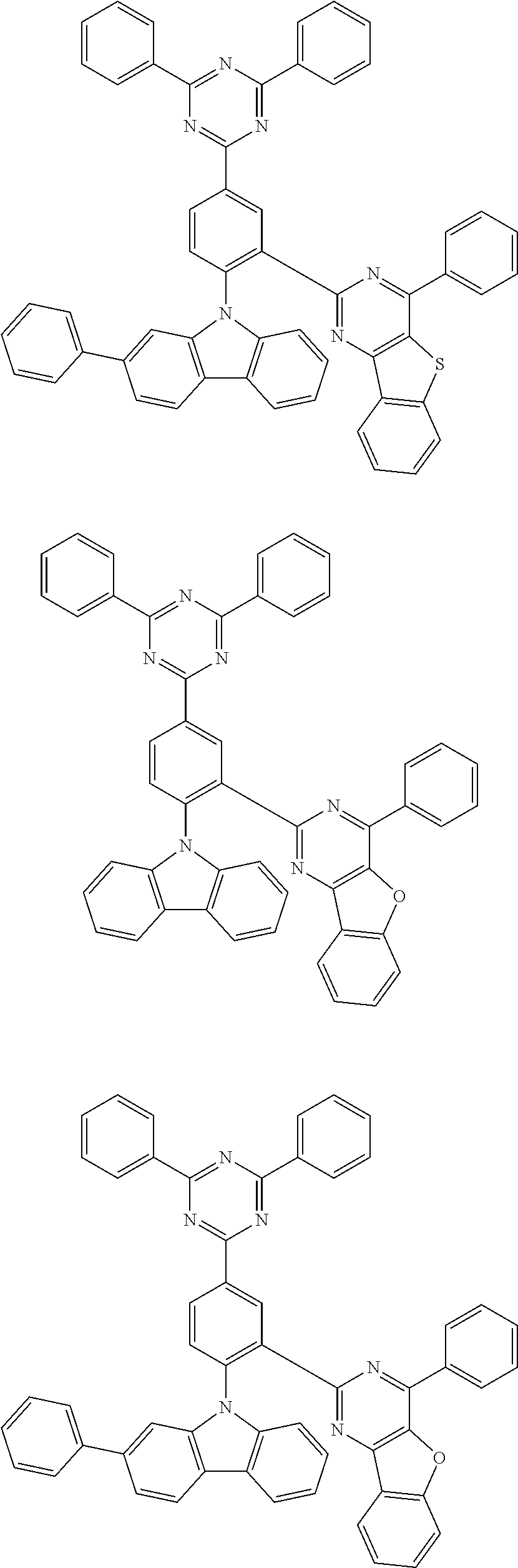
Representative examples of the compound represented by Chemical Formula 1 or 2 are as follows:
Figure US11746117-20230905-C00011
Figure US11746117-20230905-C00012
Figure US11746117-20230905-C00013
Figure US11746117-20230905-C00014
Figure US11746117-20230905-C00015
Figure US11746117-20230905-C00016
Figure US11746117-20230905-C00017
Figure US11746117-20230905-C00018
Figure US11746117-20230905-C00019
Figure US11746117-20230905-C00020
Figure US11746117-20230905-C00021
Figure US11746117-20230905-C00022
Figure US11746117-20230905-C00023
Figure US11746117-20230905-C00024
Figure US11746117-20230905-C00025
Figure US11746117-20230905-C00026
Figure US11746117-20230905-C00027
Figure US11746117-20230905-C00028
Figure US11746117-20230905-C00029
Figure US11746117-20230905-C00030
Figure US11746117-20230905-C00031
Figure US11746117-20230905-C00032
Figure US11746117-20230905-C00033
Figure US11746117-20230905-C00034
Figure US11746117-20230905-C00035
Figure US11746117-20230905-C00036
Figure US11746117-20230905-C00037
Figure US11746117-20230905-C00038
Figure US11746117-20230905-C00039
Figure US11746117-20230905-C00040
Figure US11746117-20230905-C00041
The compound represented by Chemical Formula 1 or 2 may be prepared in accordance with a preparation method as shown in Reaction Scheme 1 or 2 below.
Figure US11746117-20230905-C00042
Figure US11746117-20230905-C00043
In Reaction Schemes 1 and 2, the definitions of the substituents except X′ and X″ are the same as those described above, and X′ and X″ are each independently a halogen. Preferably, X′ is fluoro, and X″ is chloro or bromo.
The step 1 of Reaction Schemes 1 and 2 is a Suzuki coupling reaction, which is preferably carried out in the presence of a palladium catalyst and a base, and a reactive group for the Suzuki coupling reaction can be modified as known in the art. Further, the step 2 of Reaction Schemes 1 and 2 is an amine substitution reaction, which is preferably carried out in the presence of a palladium catalyst and a base, and a reactive group for the amine substitution reaction can be modified as known in the art.
The above preparation method can be further specified in the preparation examples described later.
Another embodiment of the present disclosure provides an organic light emitting device including a compound represented by Chemical Formula 1 or 2 described above. As an example, there is provided an organic light emitting device including a first electrode; a second electrode provided to face the first electrode; and one or more organic material layers provided between the first electrode and the second electrode, wherein one or more layers of the organic material layers include the compound represented by Chemical Formula 1 or 2.
The organic material layer of the organic light emitting device of the present disclosure may have a single-layer structure, or it may have a multilayered structure in which two or more organic material layers are stacked. For example, the organic light emitting device of the present disclosure may have a structure including a hole injection layer, a hole transport layer, a light emitting layer, an electron blocking layer, an electron transport layer, an electron injection layer and the like as the organic material layer. However, the structure of the organic light emitting device is not limited thereto, and it may include a smaller number of organic material layers.
Further, the organic material layer may include a light emitting layer, wherein the light emitting layer may include the compound represented by Chemical Formula 1 or 2.
Further, the organic material layer may include a hole transport layer, a hole injection layer, or a layer for simultaneously performing hole transport and hole injection, wherein the hole transport layer, the hole injection layer, or the layer for simultaneously performing hole transport and hole injection may include the compound represented by Chemical Formula 1 or 2.
Further, the electron transport layer, the electron injection layer, or the layer for simultaneously performing electron transport and electron injection may include the compound represented by Chemical Formula 1 or 2.
In addition, the organic material layer includes a light emitting layer and a hole transport layer, wherein the light emitting layer and the hole transport layer may include a compound represented by Chemical Formula 1 or 2.
Further, the organic light emitting device according to the present disclosure may be a normal type organic light emitting device in which an anode, one or more organic material layers, and a cathode are sequentially stacked on a substrate. Further, the organic light emitting device according to the present disclosure may be an inverted type organic light emitting device in which a cathode, one or more organic material layers, and an anode are sequentially stacked on a substrate. For example, the structure of an organic light emitting device according to an embodiment of the present disclosure is illustrated in FIGS. 1 and 2 .
FIG. 1 shows an example of an organic light emitting device including a substrate 1, an anode 2, an organic material layer 3, and a cathode 4. In such a structure, the compound represented by Chemical Formula 1 may be included in the organic material layer.
FIG. 2 shows an example of an organic light emitting device including a substrate 1, an anode 2, a hole injection layer 5, a hole transport layer 6, an electron blocking layer 7, a light emitting layer 8, a hole blocking layer 9, an electron transport layer 10, an electron injection layer 11, and a cathode 4. In such a structure, the compound represented by Chemical Formula 1 or 2 may be included in one or more layers of the hole injection layer, the hole transport layer, the electron blocking layer, the light emitting layer, the hole blocking layer, the electron transport layer, and the electron injection layer.
The organic light emitting device according to the present invention may be manufactured by materials and methods known in the art, except that at least one layer of the organic material layers includes the compound represented by Chemical Formula 1 or 2. In addition, when the organic light emitting device includes a plurality of organic material layers, the organic material layers may be formed of the same material or different materials.
For example, the organic light emitting device according to the present disclosure can be manufactured by sequentially stacking a first electrode, an organic material layer and a second electrode on a substrate. In this case, the organic light emitting device may be manufactured by depositing a metal, metal oxides having conductivity, or an alloy thereof on the substrate using a PVD (physical vapor deposition) method such as a sputtering method or an e-beam evaporation method to form an anode, forming organic material layers including the hole injection layer, the hole transport layer, the light emitting layer and the electron transport layer thereon, and then depositing a material that can be used as the cathode thereon. In addition to such a method, the organic light emitting device may be manufactured by sequentially depositing a cathode material, an organic material layer and an anode material on a substrate.
In addition, the compound represented by Chemical Formula 1 or 2 may be formed into an organic material layer by a solution coating method as well as a vacuum deposition method at the time of manufacturing an organic light emitting device. Herein, the solution coating method means spin coating, dip coating, doctor blading, inkjet printing, screen printing, spraying, roll coating, or the like, but is not limited thereto.
In addition to such a method, the organic light emitting device may be manufactured by sequentially depositing a cathode material, an organic material layer, and an anode material on a substrate (International Publication WO 2003/012890). However, the manufacturing method is not limited thereto.
As an example, the first electrode is an anode and the second electrode is a cathode, or the first electrode is a cathode and the second electrode is an anode.
As the anode material, generally, a material having a large work function is preferably used so that holes can be smoothly injected into the organic material layer. Specific examples of the anode material include metals such as vanadium, chromium, copper, zinc, and gold, or an alloy thereof; metal oxides such as zinc oxides, indium oxides, indium tin oxides (ITO), and indium zinc oxides (IZO); a combination of metals and oxides, such as ZnO:Al or SnO2:Sb; conductive polymers such as poly(3-methylthiophene), poly[3,4-(ethylene-1,2-dioxy)thiophene] (PEDOT), polypyrrole, and polyaniline; and the like, but are not limited thereto.
As the cathode material, generally, a material having a small work function is preferably used so that electrons can be easily injected into the organic material layer. Specific examples of the cathode material include metals such as magnesium, calcium, sodium, potassium, titanium, indium, yttrium, lithium, gadolinium, aluminum, silver, tin, and lead, or an alloy thereof; a multilayered structure material such as LiF/Al or LiO2/Al; and the like, but are not limited thereto.
The hole injection layer is a layer for injecting holes from the electrode, and the hole injection material is preferably a compound which has a capability of transporting the holes, thus has a hole injecting effect in the anode and an excellent hole injecting effect to the light emitting layer or the light emitting material, prevents excitons produced in the light emitting layer from moving to an electron injection layer or the electron injection material, and is excellent in the ability to form a thin film. It is preferable that a HOMO (highest occupied molecular orbital) of the hole injection material is between the work function of the anode material and a HOMO of a peripheral organic material layer. Specific examples of the hole injection material include metal-porphyrine, oligothiophene, an arylamine-based organic material, a hexanitrilehexaazatriphenylene-based organic material, a quinacridone-based organic material, a perylene-based organic material, anthraquinone, polyaniline and polythiophene-based conductive polymer, and the like, but are not limited thereto.
The hole transport layer is a layer that receives holes from a hole injection layer and transports the holes to the light emitting layer, and it is suitably a material having large mobility to the holes, which may receive holes from the anode or the hole injection layer and transfer the holes to the light emitting layer. Specific examples thereof include an arylamine-based organic material, a conductive polymer, a block copolymer in which a conjugate portion and a non-conjugate portion are present together, and the like, but are not limited thereto.
The electron blocking layer is a layer provided between the hole transport layer and the light emitting layer in order to prevent the electrons injected from the cathode from being transferred to the hole transport layer without being recombined in the light emitting layer, which may also be referred to as an electron inhibition layer. The electron blocking layer is preferably a material having a smaller electron affinity than the electron transport layer.
The light emitting material is preferably a material which may receive holes and electrons transported from a hole transport layer and an electron transport layer, respectively, and combine the holes and the electrons to emit light in a visible ray region, and has good quantum efficiency to fluorescence or phosphorescence. Specific examples of the light emitting material include an 8-hydroxy-quinoline aluminum complex (Alq3); a carbazole-based compound; a dimerized styryl compound; BAlq; a 10-hydroxybenzoquinoline-metal compound; a benzoxazole, benzothiazole and benzimidazole-based compound; a poly(p-phenylene vinylene) (PPV)-based polymer; a spiro compound; polyfluorene; rubrene; and the like, but are not limited thereto.
The light emitting layer may include a host material and a dopant material. The host material may be a fused aromatic ring derivative, a heterocycle-containing compound or the like. Specific examples of the fused aromatic ring derivatives include anthracene derivatives, pyrene derivatives, naphthalene derivatives, pentacene derivatives, phenanthrene compounds, and fluoranthene compounds. Examples of heterocycle-containing compounds include carbazole derivatives, dibenzofuran derivatives, ladder-type furan compounds, pyrimidine derivatives, and the like, but are not limited thereto. In one embodiment of the present invention, the compound represented by Chemical Formula 1 or Chemical Formula 2 can be used as a host material of the light emitting layer, and may achieve a low driving voltage, high efficiency, and/or long lifetime characteristics in the organic light emitting device.
Examples of the dopant material include an aromatic amine derivative, a styrylamine compound, a boron complex, a fluoranthene compound, a metal complex, and the like. Specifically, the aromatic amine derivative is a substituted or unsubstituted fused aromatic ring derivative having an arylamino group, and examples thereof include pyrene, anthracene, chrysene, periflanthene and the like, which have an arylamino group. The styrylamine compound is a compound where at least one arylvinyl group is substituted in substituted or unsubstituted arylamine in which one or two or more substituent groups selected from the group consisting of an aryl group, a silyl group, an alkyl group, a cycloalkyl group, and an arylamino group are substituted or unsubstituted. Specific examples thereof include styrylamine, styryldiamine, styryltriamine, styryltetramine, and the like, but are not limited thereto. Further, the metal complex includes an iridium complex, a platinum complex, and the like, but is not limited thereto.
The electron transport layer is a layer which receives electrons from an electron injection layer and transports the electrons to a light emitting layer, and an electron transport material is suitably a material which may receive electrons well from a cathode and transfer the electrons to a light emitting layer, and has a large mobility for electrons. Specific examples of the electron transport material include: an Al complex of 8-hydroxyquinoline; a complex including Alq3; an organic radical compound; a hydroxyflavone-metal complex, and the like, but are not limited thereto. The electron transport layer may be used with any desired cathode material, as used according to the related art. In particular, appropriate examples of the cathode material are a typical material which has a low work function, followed by an aluminum layer or a silver layer. Specific examples thereof include cesium, barium, calcium, ytterbium, and samarium, in each case followed by an aluminum layer or a silver layer.
The electron injection layer is a layer which injects electrons from an electrode, and is preferably a compound which has a capability of transporting electrons, has an effect of injecting electrons from a cathode and an excellent effect of injecting electrons into a light emitting layer or a light emitting material, prevents excitons produced from the light emitting layer from moving to a hole injection layer, and is also excellent in the ability to form a thin film. Specific examples of the electron injection layer include fluorenone, anthraquinodimethane, diphenoquinone, thiopyran dioxide, oxazole, oxadiazole, triazole, imidazole, perylenetetracarboxylic acid, fluorenylidene methane, anthrone, and the like, and derivatives thereof, a metal complex compound, a nitrogen-containing 5-membered ring derivative, and the like, but are not limited thereto.
Examples of the metal complex compound include 8-hydroxyquinolinato lithium, bis(8-hydroxyquinolinato)zinc, bis(8-hydroxyquinolinato)copper, bis(8-hydroxyquinolinato)manganese, tris(8-hydroxyquinolinato)aluminum, tris(2-methyl-8-hydroxyquinolinato)aluminum, tris(8-hydroxyquinolinato)gallium, bis(10-hydroxybenzo[h]quinolinato)beryllium, bis(10-hydroxybenzo[h]quinolinato)zinc, bis(2-methyl-8-quinolinato)chlorogallium, bis(2-methyl-8-quinolinato)(o-cresolato)gallium, bis(2-methyl-8-quinolinato)(1-naphtholato)aluminum, bis(2-methyl-8-quinolinato)(2-naphtholato)gallium, and the like, but are not limited thereto.
The organic light emitting device according to the present invention may be a front side emission type, a back side emission type, or a double side emission type according to the material used.
In addition, the compound represented by Chemical Formula 1 may be included in an organic solar cell or an organic transistor in addition to an organic light emitting device.
Hereinafter, embodiments will be described in more detail to facilitate understanding of the invention. However, the following examples are provided for illustrative purposes only and are not intended to limit the scope of the present disclosure.
PREPARATION EXAMPLES Preparation Example 1: Preparation of Compound 1
Step 1) Preparation of Compound 1-a
Figure US11746117-20230905-C00044
(5-chloro-2-fluorophenyl) boronic acid (20 g, 114.7 mmol) and 2-chloro-4,6-diphenyl-1,3,5-triazine (30.7 g, 114.7 mmol) were added to 400 ml of tetrahydrofuran under a nitrogen atmosphere, and the mixture was stirred and refluxed. Then, potassium carbonate (47.6 g, 344.1 mmol) was dissolved in 48 ml of water, added thereto and sufficiently stirred, and then tetrakistriphenyl-phosphinopalladium (4 g, 3.4 mmol) was added. After reaction for 2 hours, the reaction mixture was cooled to room temperature, the organic layer and the water layer was separated, and then the organic layer was distilled. This was added again to 830 mL of chloroform, dissolved and washed twice with water. The organic layer was then separated, anhydrous magnesium sulfate was added, stirred, and then filtered. The filtrate was distilled under reduced pressure. The concentrated compound was purified by silica gel column chromatography to give a white solid compound 1-a (32.4 g, 78%, MS: [M+H]+=362.8).
Step 2) Preparation of Compound 1-b
Figure US11746117-20230905-C00045
Compound 1-a (20 g, 55.3 mmol) and bis(pinacolato)diboron (14 g, 55.3 mmol) were added to 400 ml of dioxane under a nitrogen atmosphere, and the mixture was stirred and refluxed. Then, anhydrous potassium acetate (16.3 g, 165.8 mmol) was added thereto and sufficiently stirred, and then palladium dibenzylidene acetone palladium (1 g, 1.7 mmol) and tricyclohexylphosphine (0.9 g, 3.3 mmol) were added. After reaction for 3 hours, the reaction mixture was cooled to room temperature and then the organic layer was subjected to filtration treatment to remove a salt, and then the filtered organic layer was distilled. This was added again to 251 mL of chloroform, dissolved and washed twice with water. The organic layer was then separated, anhydrous magnesium sulfate was added, stirred, and then filtered. The filtrate was distilled under reduced pressure. The concentrated compound was purified by recrystallization with chloroform and ethanol to give a white solid 1-b (17 g, 68%, MS: [M+H]+=454.3).
Step 3) Preparation of Compound 1-c
Figure US11746117-20230905-C00046
Compound 1-b (20 g, 44.1 mmol) and 2-chloro-4-phenylbenzo[4,5]thieno[3,2-d]pyrimidine (13.1 g, 44.1 mmol) were added to 400 ml of tetrahydrofuran under a nitrogen atmosphere, and the mixture was stirred and refluxed. Then, potassium carbonate (18.3 g, 132.4 mmol) was dissolved in 18 ml of water, added thereto and sufficiently stirred, and then tetrakistriphenyl-phosphinopalladium (1.5 g, 1.3 mmol) was added. After reaction for 3 hours, the reaction mixture was cooled to room temperature and then the produced solid was filtered. The solid was added to 519 mL of choloroform, dissolved and washed twice with water. The organic layer was then separated, anhydrous magnesium sulfate was added, stirred, and then filtered. The filtrate was distilled under reduced pressure. The concentrated compound was purified by recrystallization with chloroform and ethyl acetate to give a white solid 1-c (16.6 g, 64%, MS: [M+H]+=588.7).
Step 4) Preparation of Compound 1
Figure US11746117-20230905-C00047
Compound 1-c (20 g, 34 mmol) and carbazole (5.7 g, 34 mmol) were added to 400 ml of dimethylformamide under a nitrogen atmosphere, and the mixture was stirred and refluxed. Then, cesium carbonate (33.3 g, 102.1 mmol) was added thereto and raised the temperature while stirring. After reaction for 3 hours, the reaction mixture was cooled to room temperature and then the organic layer was subjected to filtration treatment to remove a salt, and then the filtered organic layer was distilled. This was again added to 250 mL of chloroform, dissolved and washed twice with water. The organic layer was then separated, anhydrous magnesium sulfate was added, stirred, and then filtered. The filtrate was distilled under reduced pressure. The concentrated compound was purified by silica gel column chromatography and sublimation purification to give compound 1 (12.8 g, 51%, MS: [M+H]+=735.9).
Preparation Example 2: Preparation of Compound 2
Figure US11746117-20230905-C00048
Compound 2 was prepared in the same manner as the preparation method of Compound 1, except that 2-chloro-4-phenylquinazoline was used instead of 2-chloro-4-phenylbenzo[4,5]thieno[3,2-d]pyrimidine in Step 3 of Preparation Example 1 (MS [M+H]+=679.8).
Preparation Example 3: Preparation of Compound 3
Figure US11746117-20230905-C00049
Compound 3 was prepared in the same manner as the preparation method of Compound 1, except that 2-chloro-4-phenylbenzofuro[3,2-d]pyrimidine was used instead of 2-chloro-4-phenylbenzo[4,5]thieno[3,2-d]pyrimidine in Step 3 of Preparation Example 1 (MS [M+H]+=719.8).
Preparation Example 4: Preparation of Compound 4
Figure US11746117-20230905-C00050
Figure US11746117-20230905-C00051
Compound 4 was prepared in the same manner as the preparation Example 1, except that 2-chloro-4,6-bis(phenyl-d5)-1,3,5-triazine was used instead of 2-chloro-4,6-diphenyl-1,3,5-triazine (MS [M+H]+=745.0).
Preparation Example 5: Preparation of Compound 5
Figure US11746117-20230905-C00052
Figure US11746117-20230905-C00053
Compound 5 was prepared in the same manner as Preparation Example 1, except that 2-chloro-4-(dibenzo[b,d]furan-1-yl)-6-phenyl-1,3,5-triazine was used instead of 2-chloro-4,6-diphenyl-1,3,5-triazine (MS [M+H]+=826.0).
Preparation Example 6: Preparation of Compound 6
Step 1) Preparation of Compound 6-a
Figure US11746117-20230905-C00054
2-chloro-4,6-diphenyl-1,3,5-triazine (20 g, 74.7 mmol) and (3-chloro-4-fluorophenyl)boronic acid (13 g, 74.7 mmol) were added to 400 ml of tetrahydrofuran under a nitrogen atmosphere, and the mixture was stirred and refluxed. Then, potassium carbonate (31 g, 224.1 mmol) was dissolved in 31 ml of water, added thereto and sufficiently stirred, and then tetrakis triphenyl-phosphinopalladium (2.6 g, 2.2 mmol) was added. After reaction for 2 hours, the reaction mixture was cooled to room temperature, the organic layer and the water layer was separated, and then the organic layer was distilled. This was added again to 541 mL of choloroform, dissolved and washed twice with water. The organic layer was then separated, anhydrous magnesium sulfate was added, stirred, and then filtered. The filtrate was distilled under reduced pressure. The concentrated compound was purified by silica gel column chromatography to give a white solid compound 6-a (21.6 g, 80%, MS: [M+H]+=362.8).
Step 2) Preparation of Compound 6-b
Figure US11746117-20230905-C00055
Compound 6-a (20 g, 55.3 mmol) and bis(pinacolato)diboron (14 g, 55.3 mmol) were added to 400 ml of dioxane under a nitrogen atmosphere, and the mixture was stirred and refluxed. Then, anhydrous potassium acetate (16.3 g, 165.8 mmol) was added thereto and sufficiently stirred, and then bis(dibenzylideneacetone)palladium (1 g, 1.7 mmol) and tricyclohexylphosphine (0.9 g, 3.3 mmol) were added. After reaction for 3 hours, the reaction mixture was cooled to room temperature and then the organic layer was subjected to filtration treatment to remove a salt, and then the filtered organic layer was distilled. This was added again to 251 mL of chloroform, dissolved and washed twice with water. The organic layer was then separated, anhydrous magnesium sulfate was added, stirred, and then filtered. The filtrate was distilled under reduced pressure. The concentrated compound was purified by recrystallization with chloroform and ethanol to give a white solid 6-b (18.5 g, 74%, MS: [M+H]+=454.3).
Step 3) Preparation of Compound 6-c
Figure US11746117-20230905-C00056
Compound 6-b (20 g, 44.1 mmol) and 2-chloro-4-phenylbenzo[4,5]thieno[3,2-d]pyrimidine (13.1 g, 44.1 mmol) were added to 400 ml of tetrahydrofuran under a nitrogen atmosphere, and the mixture was stirred and refluxed. Then, potassium carbonate (18.3 g, 132.4 mmol) was dissolved in 18 ml of water, added thereto and sufficiently stirred, and then tetrakistriphenyl-phosphinopalladium (1.5 g, 1.3 mmol) was added. After reaction for 3 hours, the reaction mixture was cooled to room temperature and then the produced solid was filtered. The solid was added to 519 mL of choloroform, dissolved and washed twice with water. The organic layer was then separated, anhydrous magnesium sulfate was added, stirred, and then filtered. The filtrate was distilled under reduced pressure. The concentrated compound was purified by recrystallization with chloroform and ethyl acetate to give a white solid 6-c (13 g, 50%, MS: [M+H]+=588.7).
Step 4) Preparation of Compound 6
Figure US11746117-20230905-C00057
Compound 6-c (20 g, 34 mmol) and carbazole (5.7 g, 34 mmol) were added to 400 ml of dimethyl formamide under a nitrogen atmosphere, and the mixture was stirred and refluxed. Then, cesium carbonate (33.3 g, 102.1 mmol) was added thereto and the temperature was raised while stirring. After reaction for 3 hours, the reaction mixture was cooled to room temperature and then the organic layer was subjected to filtration treatment to remove a salt, and then the filtered organic layer was distilled. This was again added to 250 mL of chloroform, dissolved and washed twice with water. The organic layer was then separated, anhydrous magnesium sulfate was added, stirred, and then filtered. The filtrate was distilled under reduced pressure. The concentrated compound was purified by silica gel column chromatography and sublimation purification to give compound 6 (15.5 g, 62%, MS: [M+H]+=735.9).
Preparation Example 7: Preparation of Compound 7
Figure US11746117-20230905-C00058
Compound 7 was prepared in the same manner as the preparation method of Compound 6, except that 2-chloro-4-phenylquinazoline was used instead of 2-chloro-4-phenylbenzo[4,5]thieno[3,2-d]pyrimidine in Step 3 of Preparation Example 6 (MS [M+H]+=679.8).
Preparation Example 8: Preparation of Compound 8
Figure US11746117-20230905-C00059
Compound 8 was prepared in the same manner as the preparation method of Compound 6, except that 2-chloro-4-phenylbenzofuro[3,2-d]pyrimidine was used instead of 2-chloro-4-phenylbenzo[4,5]thieno[3,2-d]pyrimidine in Step 3 of Preparation Example 6 (MS [M+H]+=719.8).
EXAMPLES Example 1
A glass substrate on which ITO (indium tin oxide) was coated as a thin film to a thickness of 1400 Å was put into distilled water in which a detergent was dissolved, and ultrasonically cleaned. At this time, a product manufactured by Fischer Co. was used as the detergent, and as the distilled water, distilled water filtered twice using a filter manufactured by Millipore Co. was used. After the ITO was cleaned for 30 minutes, ultrasonic cleaning was repeated twice using distilled water for 10 minutes. After the cleaning with distilled water was completed, the substrate was ultrasonically cleaned with solvents of isopropyl alcohol, acetone, and methanol, dried, and then transferred to a plasma cleaner. In addition, the substrate was cleaned for 5 minutes using oxygen plasma and then transferred to a vacuum depositor.
On the ITO transparent electrode thus prepared, a compound HT-A and a compound PD below were thermally vacuum-deposited to a thickness of 100 Å in a weight ratio of 95:5, and then the compound HT-A was deposited to a thickness of 1150 Å to form a hole transport layer. A compound HT-B below was thermally vacuum-deposited to a thickness of 450 Å on the hole transport layer to form an electron blocking layer. Compound 1 prepared in the previous preparation example and a compound GD below were deposited in a weight ratio of 85:15 on the electron blocking layer with a thickness of 400 Å to form a light emitting layer. A compound ET-A below was vacuum-deposited to a thickness of 50 Å on the light emitting layer to form a hole blocking layer. A compound ET-B and a compound Liq below were thermally vacuum-deposited in a weight ratio of 2:1 on the hole blocking layer with a thickness of 250 Å, and then LiF and magnesium were vacuum-deposited in a weight ratio of 1:1 with a thickness of 30 Å to form an electron transport and injection layer. Magnesium and silver were deposited to a thickness of 160 Å in a weight ratio of 1:4 on the electron transport and injection layer to form a cathode, to prepare an organic emitting device.
Figure US11746117-20230905-C00060
Figure US11746117-20230905-C00061
In the above-mentioned process, the vapor deposition rate of the organic material was maintained at 0.4˜0.7 Å/sec, the deposition rate of lithium fluoride of anode was maintained at 0.3 Å/sec, the deposition rate of silver and magnesium was maintained at 2 Å/sec, and the degree of vacuum during the deposition was maintained 2×10⁻⁷ to 5×10⁻⁶ torr to form an organic light emitting device.
Examples 2 to 8
The organic light emitting devices were manufactured in the same manner as in Example 1, except that the compounds shown in Table 1 below were used instead of Compound 1.
Comparative Examples 1 to 3
The organic light emitting devices were manufactured in the same manner as in Example 1, except that the compounds shown in Table 1 below were used instead of Compound 1. In Table 1, the compounds GH-A, GH-B and GH-C are as follows.
Figure US11746117-20230905-C00062
Experimental Example
The voltage, efficiency, and lifetime (T95) of the organic light emitting devices manufactured in the examples and comparative examples were measured by applying current, and the results are shown in Table 1 below. At this time, the voltage and efficiency were measured at a current density of 10 mA/cm2. Further, the T95 means the time required for the luminance to be reduced to 95% of the initial luminance at a current density of 20 mA/cm2.
TABLE 1
Light emitting Voltage Efficiency Lifetime
layer (host) (V) (cd/A) (T95, hr)
Example 1 compound 1 4.98 38.2 83
Example 2 compound 2 5.03 36.2 92
Example 3 compound 3 4.95 37.1 82
Example 4 compound 4 4.97 38.3 93
Example 5 compound 5 5.09 36.1 71
Example 6 compound 6 5.05 36.9 83
Example 7 compound 7 5.11 37.3 82
Example 8 compound 8 5.19 37.6 85
Comparative GH-A 5.12 33.2 43
Example 1
Comparative GH-B 5.21 33.8 56
Example 2
Comparative GH-C 6.12 27.5 50
Example 3
In the compound represented by Chemical Formula 1 and 2, an intra charge transfer can be easily occur since a carbazole group having hole transferring characteristics is in ortho position with triazine, benzothienopyrimidine, quinazoline, or benzofuropyrimidine, which have electron transferring characteristics. Thus, molecular stability is high and the compound is advantageous for both hole and electron transport. In addition, the electron transport characteristics may be adjusted variously with the combination of Ar1, Ar2, and E of Chemical Formula 1 or 2, and therefore the compound is advantageous in balancing charges in accordance with change of the common layer.
Therefore, as shown in Table 1, when the compound represented by Chemical Formula 1 or 2 was used as a host material of organic light emitting device, it was confirmed that it exhibited low driving voltage, high efficiency, and long lifetime characteristics as compared with Comparative Examples having similar molecular structure.
<Description of Reference Numerals>
 1: substrate  2: anode
 3: organic material layer  4: cathode
 5: hole injection layer  6: hole transport layer
 7: electron blocking layer  8: light emitting layer
 9: hole blocking layer 10: electron transport layer
11: electron injection layer

Claims (9)

The invention claimed is:
1. A compound represented by Chemical Formula 1 or 2:
Figure US11746117-20230905-C00063
wherein, in Chemical Formulas 1 and 2,
X1 to X3 are each independently, CH or N, and at least one of X1 to X3 is N,
Ar1 and Ar2 are each independently a substituted or unsubstituted C6-60 aryl; or a substituted or unsubstituted C2-60 heteroaryl containing at least one heteroatom selected from the group consisting of N, O, and S,
R1 is each independently deuterium; a substituted or unsubstituted C6-60 aryl; or a substituted or unsubstituted C2-60 heteroaryl containing at least one heteroatom selected from the group consisting of N, O, and S,
n is an integer of 0 to 8,
E is a substituent represented by Chemical Formula 3-1 or 3-2,
Figure US11746117-20230905-C00064
wherein, in Chemical Formulas 3-1 and 3-2,
X4 and X5 are each independently, CH or N, and at least one of X4 and X5 is N,
Ar3 is a substituted or unsubstituted C6-60 aryl; or a substituted or unsubstituted C2-60 heteroaryl containing at least one heteroatom selected from the group consisting of N, O, and S,
wherein A is represented by Chemical Formula 4-1 or 4-2,
Figure US11746117-20230905-C00065
wherein, in Chemical Formulas 4-1 and 4-2,
* Is a bond shared with an adjacent hexagonal ring,
Y is O, S, C(R′)2, or NR′,
R′ is each independently hydrogen; deuterium; a substituted or unsubstituted C6-60 aryl; or a substituted or unsubstituted C2-60 heteroaryl containing at least one heteroatom selected from the group consisting of N, O, and S.
2. The compound of claim 1, wherein
R1 is phenyl.
3. The compound of claim 1, wherein
all of X1 to X3 are N.
4. The compound of claim 1, wherein
E is any one selected from the group consisting of the following:
Figure US11746117-20230905-C00066
wherein, Ar3, X4, X5, and Y are the same as those defined in claim 1.
5. The compound of claim 1, wherein
both X4 and X5 are N.
6. The compound of claim 1, wherein
Y is O or S.
7. The compound of claim 1, wherein
Ar1 to Ar3 are each independently phenyl, biphenyl, phenyl substituted with five deuteriums, or dibenzofuranyl.
8. The compound of claim 1, wherein
the compound is any one selected from the group consisting of the following:
Figure US11746117-20230905-C00067
Figure US11746117-20230905-C00068
Figure US11746117-20230905-C00069
Figure US11746117-20230905-C00070
Figure US11746117-20230905-C00071
Figure US11746117-20230905-C00072
Figure US11746117-20230905-C00073
Figure US11746117-20230905-C00074
Figure US11746117-20230905-C00075
Figure US11746117-20230905-C00076
Figure US11746117-20230905-C00077
Figure US11746117-20230905-C00078
Figure US11746117-20230905-C00079
Figure US11746117-20230905-C00080
Figure US11746117-20230905-C00081
Figure US11746117-20230905-C00082
Figure US11746117-20230905-C00083
Figure US11746117-20230905-C00084
Figure US11746117-20230905-C00085
Figure US11746117-20230905-C00086
Figure US11746117-20230905-C00087
Figure US11746117-20230905-C00088
Figure US11746117-20230905-C00089
Figure US11746117-20230905-C00090
Figure US11746117-20230905-C00091
Figure US11746117-20230905-C00092
Figure US11746117-20230905-C00093
Figure US11746117-20230905-C00094
Figure US11746117-20230905-C00095
Figure US11746117-20230905-C00096
Figure US11746117-20230905-C00097
9. An organic light emitting device comprising a first electrode; a second electrode provided to face the first electrode; and one or more organic material layers provided between the first electrode and the second electrode, wherein at least one layer of the organic material layers includes the compound according to claim 1.
US17/275,664 2018-11-27 2019-11-14 Heterocyclic compound and organic light emitting device comprising same Active 2040-10-03 US11746117B2 (en)

Applications Claiming Priority (5)

Application Number Priority Date Filing Date Title
KR20180148563 2018-11-27
KR10-2018-0148563 2018-11-27
KR1020190145261A KR102265929B1 (en) 2018-11-27 2019-11-13 Novel compound and organic light emitting device comprising the same
KR10-2019-0145261 2019-11-13
PCT/KR2019/015558 WO2020111602A1 (en) 2018-11-27 2019-11-14 Novel compound and organic light-emitting element including same

Publications (2)

Publication Number Publication Date
US20220056047A1 US20220056047A1 (en) 2022-02-24
US11746117B2 true US11746117B2 (en) 2023-09-05

Family

ID=70851832

Family Applications (1)

Application Number Title Priority Date Filing Date
US17/275,664 Active 2040-10-03 US11746117B2 (en) 2018-11-27 2019-11-14 Heterocyclic compound and organic light emitting device comprising same

Country Status (2)

Country Link
US (1) US11746117B2 (en)
WO (1) WO2020111602A1 (en)

Families Citing this family (1)

* Cited by examiner, † Cited by third party
Publication number Priority date Publication date Assignee Title
CN114075210B (en) * 2020-08-13 2023-02-24 上海和辉光电股份有限公司 Electron transport material and organic electroluminescent device

Citations (64)

* Cited by examiner, † Cited by third party
Publication number Priority date Publication date Assignee Title
KR20000051826A (en) 1999-01-27 2000-08-16 성재갑 New organomattalic complex molecule for the fabrication of organic light emitting diodes
WO2003012890A2 (en) 2001-07-20 2003-02-13 Novaled Gmbh Light emitting component with organic layers
CN101087776A (en) 2004-12-24 2007-12-12 先锋公司 Organic compound, charge-transporting material, and organic electroluminescent element
CN100366703C (en) 2002-03-22 2008-02-06 出光兴产株式会社 Material for organic electroluminescent device and organic electroluminescent device using the same
JP2009155300A (en) 2007-12-27 2009-07-16 Idemitsu Kosan Co Ltd Material for organic electroluminescent element and organic electroluminescent element using the same
JP2009158848A (en) 2007-12-27 2009-07-16 Idemitsu Kosan Co Ltd Material for organic electroluminescent element, and organic electroluminescent element using the material
JP2010030937A (en) 2008-07-28 2010-02-12 Chemiprokasei Kaisha Ltd New dicarbazolylphenyl derivative, host material obtained by using the same, and organic electroluminescent element
JP4474493B1 (en) 2009-07-31 2010-06-02 富士フイルム株式会社 Organic electroluminescence device
JP4590020B1 (en) 2009-07-31 2010-12-01 富士フイルム株式会社 Charge transport material and organic electroluminescent device
KR20100131939A (en) 2009-06-08 2010-12-16 에스에프씨 주식회사 Indolocarbazole derivatives and organoelectroluminescent device using the same
JP4729642B1 (en) 2010-07-09 2011-07-20 富士フイルム株式会社 Organic electroluminescence device
WO2012005362A1 (en) 2010-07-09 2012-01-12 富士フイルム株式会社 Organic electroluminescent element
KR20120033711A (en) 2010-09-30 2012-04-09 (주)씨에스엘쏠라 Organic light emitting compound and organic light emitting device comprising the same
US20120205640A1 (en) 2009-10-23 2012-08-16 Takahiro Kai Organic electroluminescent device
KR20120109744A (en) 2011-03-25 2012-10-09 롬엔드하스전자재료코리아유한회사 Novel compounds for organic electronic material and organic electroluminescence device using the same
KR20130020398A (en) 2011-08-19 2013-02-27 제일모직주식회사 Compound for organic optoelectronic device, organic light emitting diode including the same and display including the organic light emitting diode
KR20130130236A (en) 2011-05-03 2013-12-02 롬엔드하스전자재료코리아유한회사 Novel organic electroluminescent compounds and an organic electroluminescent device using the same
KR20140014959A (en) 2012-07-27 2014-02-06 (주)피엔에이치테크 Novel compound for organic electroluminescent device and organic electroluminescent device comprising the same
JP2014141571A (en) 2013-01-23 2014-08-07 Kyushu Univ Light emitting material and organic light emitting element using the same
KR20140139307A (en) 2013-05-27 2014-12-05 제일모직주식회사 COMPOUND, ORGANIC LiGHT EMITTING DIODE INCLUDING THE SAME AND DISPLAY INCLUDING THE ORGANIC LiGHT EMITTING DIODE
KR20150061174A (en) 2013-11-26 2015-06-04 주식회사 두산 Organic compounds and organic electro luminescence device comprising the same
KR20150063462A (en) 2012-09-28 2015-06-09 신닛테츠 수미킨 가가쿠 가부시키가이샤 Compound for organic electroluminescent elements, and organic electroluminescent element
KR20150105201A (en) 2014-03-05 2015-09-16 주식회사 엠비케이 New organic electroluminescent compounds and organic electroluminescent device comprising the same
KR20150129282A (en) 2014-05-09 2015-11-19 주식회사 엠비케이 Novel compoung for organic electroluminescent device, organic electroluminescent device including the same and electric apparatus
KR20150139459A (en) 2014-06-03 2015-12-11 유니버셜 디스플레이 코포레이션 Organic electroluminescent materials and devices
US20150380662A1 (en) 2014-06-30 2015-12-31 Samsung Display Co., Ltd. Organic light-emitting device
KR20160041768A (en) 2014-10-08 2016-04-18 주식회사 알파켐 New host material and organic electroluminescent device using the same
WO2016089080A1 (en) 2014-12-02 2016-06-09 주식회사 두산 Organic luminescent compound and organic electroluminescent device comprising same
KR20160129190A (en) 2015-04-29 2016-11-09 삼성디스플레이 주식회사 Organic light emitting device
US20160329502A1 (en) 2015-05-07 2016-11-10 Universal Display Corporation Organic Electroluminescent Materials and Devices
WO2016181846A1 (en) 2015-05-08 2016-11-17 コニカミノルタ株式会社 Π-conjugated compound, organic electroluminescence element material, light-emitting material, light-emitting thin film, organic electroluminescence element, display device, and illumination device
US20170047522A1 (en) 2014-03-07 2017-02-16 Kyulux, Inc. Light-emitting material, organic light-emitting device, and compound
US9577199B2 (en) 2009-02-27 2017-02-21 E I Du Pont Nemours And Company Deuterated compounds for electronic applications
US20170117488A1 (en) 2014-04-08 2017-04-27 Rohm And Haas Electronic Materials Korea Ltd. Multi-component host material and organic electroluminescent device comprising the same
KR20170049291A (en) 2015-10-28 2017-05-10 희성소재 (주) Hetero-cyclic compound and organic light emitting device using the same
KR20170060836A (en) 2015-11-25 2017-06-02 에스케이케미칼주식회사 Compound for organic electroluminescent device and organic electroluminescent device comprising the same
KR20170076292A (en) 2015-12-24 2017-07-04 주식회사 두산 Organic light-emitting compound and organic electroluminescent device using the same
KR20170079348A (en) 2015-12-30 2017-07-10 엘지디스플레이 주식회사 Organic compound, and Organic light emitting diode and Organic light emitting diode display device including the same
US20170244043A1 (en) 2016-02-18 2017-08-24 Samsung Display Co., Ltd. Organic light-emitting device
KR20170113808A (en) 2016-03-25 2017-10-13 단국대학교 산학협력단 TADF Material and OLED Having the Same
KR20170116993A (en) 2016-04-12 2017-10-20 주식회사 엘지화학 Compound and organic electronic device comprising the same
WO2017190885A1 (en) 2016-05-04 2017-11-09 Cynora Gmbh Organic molecules, especially for use in optoelectronic devices
DE102016112377A1 (en) 2016-07-06 2018-01-11 Cynora Gmbh Organic molecules, in particular for use in organic optoelectronic devices
CN107667102A (en) 2015-03-27 2018-02-06 檀国大学校产学协力团 Ortho position substitutes hot activation delayed fluorescence material and includes this organic illuminating element
JP2018035129A (en) 2015-10-27 2018-03-08 国立大学法人山形大学 Pyrimidine derivative, luminescent material consisting of the same and organic el element using the same
CN107880028A (en) 2016-09-30 2018-04-06 江苏三月光电科技有限公司 A kind of compound and organic electroluminescence device using pyridine as core
CN107935914A (en) 2017-11-28 2018-04-20 上海道亦化工科技有限公司 A kind of two carbazole benzene derivatives and application thereof and organic electroluminescence device
CN107987009A (en) 2017-11-28 2018-05-04 上海道亦化工科技有限公司 A kind of carbazole derivates and application thereof and organic electroluminescence device
KR20180047306A (en) 2016-10-31 2018-05-10 성균관대학교산학협력단 Delayed fluorescence material and organic light emitting device having the delayed fluorescence material
US20180145262A1 (en) 2016-11-21 2018-05-24 Universal Display Corporation Organic Electroluminescent Materials and Devices
KR20180063708A (en) 2016-12-02 2018-06-12 (주)피엔에이치테크 An electroluminescent compound and an electroluminescent device comprising the same
KR20180065276A (en) 2016-12-07 2018-06-18 주식회사 엘지화학 Hetero-cyclic compound and organic light emitting device comprising the same
WO2018147638A1 (en) 2017-02-08 2018-08-16 주식회사 두산 Organic compound and organic electroluminescent element using same
US20180248127A1 (en) 2017-02-27 2018-08-30 Samsung Electronics Co., Ltd. Condensed cyclic compound and organic light-emitting device including the same
KR20180109747A (en) 2017-03-27 2018-10-08 주식회사 엘지화학 Benzocarbazole-based compound and organic light emitting device comprising the same
KR101926771B1 (en) 2018-03-02 2018-12-07 주식회사 진웅산업 Organic light emitting diode comprising phosphorescence green host materials having thermally activated delayed fluorescence properties
WO2018237385A1 (en) 2017-06-23 2018-12-27 Kyulux, Inc. Composition of matter for use in organic light-emitting diodes
US20190019960A1 (en) * 2017-07-14 2019-01-17 Cynora Gmbh Organic molecules, in particular for use in optoelectronic devices
WO2019076844A1 (en) 2017-10-18 2019-04-25 Cynora Gmbh Organic molecules, in particular for use in optoelectronic devices
WO2019086297A1 (en) 2017-10-30 2019-05-09 Cynora Gmbh Organic molecules for use in optoelectronic devices
WO2019121112A1 (en) * 2017-12-21 2019-06-27 Cynora Gmbh Organic molecules for use in optoelectronic devices
KR20190108094A (en) 2017-04-06 2019-09-23 덕산네오룩스 주식회사 Compound for organic electronic element, organic electronic element using the same, and an electronic device thereof
KR20200047418A (en) 2018-10-26 2020-05-07 주식회사 엘지화학 Deuterium-comprising compound and organic light emitting device comprising same
KR20200063053A (en) 2018-11-27 2020-06-04 주식회사 엘지화학 Novel compound and organic light emitting device comprising the same

Patent Citations (93)

* Cited by examiner, † Cited by third party
Publication number Priority date Publication date Assignee Title
KR20000051826A (en) 1999-01-27 2000-08-16 성재갑 New organomattalic complex molecule for the fabrication of organic light emitting diodes
WO2003012890A2 (en) 2001-07-20 2003-02-13 Novaled Gmbh Light emitting component with organic layers
US20040251816A1 (en) 2001-07-20 2004-12-16 Karl Leo Light emitting component with organic layers
CN100366703C (en) 2002-03-22 2008-02-06 出光兴产株式会社 Material for organic electroluminescent device and organic electroluminescent device using the same
CN101087776A (en) 2004-12-24 2007-12-12 先锋公司 Organic compound, charge-transporting material, and organic electroluminescent element
US20090191426A2 (en) 2004-12-24 2009-07-30 Pioneer Corporation Organic compound, charge-transporting material, and organic electroluminescent element
JP2009155300A (en) 2007-12-27 2009-07-16 Idemitsu Kosan Co Ltd Material for organic electroluminescent element and organic electroluminescent element using the same
JP2009158848A (en) 2007-12-27 2009-07-16 Idemitsu Kosan Co Ltd Material for organic electroluminescent element, and organic electroluminescent element using the material
JP2010030937A (en) 2008-07-28 2010-02-12 Chemiprokasei Kaisha Ltd New dicarbazolylphenyl derivative, host material obtained by using the same, and organic electroluminescent element
US9577199B2 (en) 2009-02-27 2017-02-21 E I Du Pont Nemours And Company Deuterated compounds for electronic applications
KR20100131939A (en) 2009-06-08 2010-12-16 에스에프씨 주식회사 Indolocarbazole derivatives and organoelectroluminescent device using the same
JP4474493B1 (en) 2009-07-31 2010-06-02 富士フイルム株式会社 Organic electroluminescence device
JP4590020B1 (en) 2009-07-31 2010-12-01 富士フイルム株式会社 Charge transport material and organic electroluminescent device
US20120126692A1 (en) 2009-07-31 2012-05-24 Fujifilm Corporation Organic electroluminescence device
KR20120018231A (en) 2009-07-31 2012-02-29 후지필름 가부시키가이샤 Organic electroluminescence device
US20120126221A1 (en) 2009-07-31 2012-05-24 Fujifilm Corporation Charge-transporting material and organic electroluminescence device
US20120205640A1 (en) 2009-10-23 2012-08-16 Takahiro Kai Organic electroluminescent device
KR20120098694A (en) 2009-10-23 2012-09-05 신닛테츠가가쿠 가부시키가이샤 Organic electroluminescent element
WO2012005362A1 (en) 2010-07-09 2012-01-12 富士フイルム株式会社 Organic electroluminescent element
JP4729642B1 (en) 2010-07-09 2011-07-20 富士フイルム株式会社 Organic electroluminescence device
US20130292654A1 (en) 2010-07-09 2013-11-07 Udc Ireland Limited Organic Electroluminescent Element
KR20140015240A (en) 2010-07-09 2014-02-06 유디씨 아일랜드 리미티드 Organic electroluminescent element
KR20120033711A (en) 2010-09-30 2012-04-09 (주)씨에스엘쏠라 Organic light emitting compound and organic light emitting device comprising the same
KR20120109744A (en) 2011-03-25 2012-10-09 롬엔드하스전자재료코리아유한회사 Novel compounds for organic electronic material and organic electroluminescence device using the same
US20140114069A1 (en) 2011-03-25 2014-04-24 Ronm and Haas Electronic Materials Korea Ltd. Novel compounds for organic electronic material and organic electroluminescent device using the same
CN103764786A (en) 2011-05-03 2014-04-30 罗门哈斯电子材料韩国有限公司 Novel organic electroluminescent compounds and an organic electroluminescent device using the same
KR20130130236A (en) 2011-05-03 2013-12-02 롬엔드하스전자재료코리아유한회사 Novel organic electroluminescent compounds and an organic electroluminescent device using the same
KR101396171B1 (en) 2011-05-03 2014-05-27 롬엔드하스전자재료코리아유한회사 Novel organic electroluminescent compounds and an organic electroluminescent device using the same
WO2013027906A1 (en) 2011-08-19 2013-02-28 제일모직 주식회사 Compound for an organic optoelectric device, organic light emitting element including same, and display device including the organic light emitting element
KR20130020398A (en) 2011-08-19 2013-02-27 제일모직주식회사 Compound for organic optoelectronic device, organic light emitting diode including the same and display including the organic light emitting diode
KR20140014959A (en) 2012-07-27 2014-02-06 (주)피엔에이치테크 Novel compound for organic electroluminescent device and organic electroluminescent device comprising the same
KR20150063462A (en) 2012-09-28 2015-06-09 신닛테츠 수미킨 가가쿠 가부시키가이샤 Compound for organic electroluminescent elements, and organic electroluminescent element
US20150218191A1 (en) 2012-09-28 2015-08-06 Nippon Steel & Sumikin Chemical Co., Ltd. Compound for organic electroluminescent elements, and organic electroluminescent element
JP2014141571A (en) 2013-01-23 2014-08-07 Kyushu Univ Light emitting material and organic light emitting element using the same
KR20140139307A (en) 2013-05-27 2014-12-05 제일모직주식회사 COMPOUND, ORGANIC LiGHT EMITTING DIODE INCLUDING THE SAME AND DISPLAY INCLUDING THE ORGANIC LiGHT EMITTING DIODE
KR20150061174A (en) 2013-11-26 2015-06-04 주식회사 두산 Organic compounds and organic electro luminescence device comprising the same
KR20150105201A (en) 2014-03-05 2015-09-16 주식회사 엠비케이 New organic electroluminescent compounds and organic electroluminescent device comprising the same
US20170047522A1 (en) 2014-03-07 2017-02-16 Kyulux, Inc. Light-emitting material, organic light-emitting device, and compound
KR20180027468A (en) 2014-04-08 2018-03-14 롬엔드하스전자재료코리아유한회사 Multi-component host material and organic electroluminescence device comprising the same
US20170117488A1 (en) 2014-04-08 2017-04-27 Rohm And Haas Electronic Materials Korea Ltd. Multi-component host material and organic electroluminescent device comprising the same
KR20150129282A (en) 2014-05-09 2015-11-19 주식회사 엠비케이 Novel compoung for organic electroluminescent device, organic electroluminescent device including the same and electric apparatus
KR20150139459A (en) 2014-06-03 2015-12-11 유니버셜 디스플레이 코포레이션 Organic electroluminescent materials and devices
KR20160003362A (en) 2014-06-30 2016-01-11 삼성디스플레이 주식회사 Organic light-emitting device
US20150380662A1 (en) 2014-06-30 2015-12-31 Samsung Display Co., Ltd. Organic light-emitting device
KR20160041768A (en) 2014-10-08 2016-04-18 주식회사 알파켐 New host material and organic electroluminescent device using the same
KR20160066339A (en) 2014-12-02 2016-06-10 주식회사 두산 Organic compounds and organic electro luminescence device comprising the same
WO2016089080A1 (en) 2014-12-02 2016-06-09 주식회사 두산 Organic luminescent compound and organic electroluminescent device comprising same
US20180123049A1 (en) 2015-03-27 2018-05-03 Industry-Academic Cooperation Foundation, Dankook University Ortho-substituted thermally activated delayed fluorescence material and organic light-emitting device comprising same
CN107667102A (en) 2015-03-27 2018-02-06 檀国大学校产学协力团 Ortho position substitutes hot activation delayed fluorescence material and includes this organic illuminating element
KR20160129190A (en) 2015-04-29 2016-11-09 삼성디스플레이 주식회사 Organic light emitting device
US20160329502A1 (en) 2015-05-07 2016-11-10 Universal Display Corporation Organic Electroluminescent Materials and Devices
WO2016181846A1 (en) 2015-05-08 2016-11-17 コニカミノルタ株式会社 Π-conjugated compound, organic electroluminescence element material, light-emitting material, light-emitting thin film, organic electroluminescence element, display device, and illumination device
US20180170914A1 (en) 2015-05-08 2018-06-21 Konica Minolta, Inc. Ii(pi)-conjugated compound, organic electroluminescence element material, light-emitting material, light-emitting thin film, organic electroluminescence element, display device, and illumination device
JP2018035129A (en) 2015-10-27 2018-03-08 国立大学法人山形大学 Pyrimidine derivative, luminescent material consisting of the same and organic el element using the same
KR20170049291A (en) 2015-10-28 2017-05-10 희성소재 (주) Hetero-cyclic compound and organic light emitting device using the same
KR20170060836A (en) 2015-11-25 2017-06-02 에스케이케미칼주식회사 Compound for organic electroluminescent device and organic electroluminescent device comprising the same
KR20170076292A (en) 2015-12-24 2017-07-04 주식회사 두산 Organic light-emitting compound and organic electroluminescent device using the same
KR20170079348A (en) 2015-12-30 2017-07-10 엘지디스플레이 주식회사 Organic compound, and Organic light emitting diode and Organic light emitting diode display device including the same
KR20170097820A (en) 2016-02-18 2017-08-29 삼성디스플레이 주식회사 Organic light emitting device
US20170244043A1 (en) 2016-02-18 2017-08-24 Samsung Display Co., Ltd. Organic light-emitting device
KR20170113808A (en) 2016-03-25 2017-10-13 단국대학교 산학협력단 TADF Material and OLED Having the Same
KR20170116993A (en) 2016-04-12 2017-10-20 주식회사 엘지화학 Compound and organic electronic device comprising the same
WO2017190885A1 (en) 2016-05-04 2017-11-09 Cynora Gmbh Organic molecules, especially for use in optoelectronic devices
DE102016112377A1 (en) 2016-07-06 2018-01-11 Cynora Gmbh Organic molecules, in particular for use in organic optoelectronic devices
CN107880028A (en) 2016-09-30 2018-04-06 江苏三月光电科技有限公司 A kind of compound and organic electroluminescence device using pyridine as core
KR20180047306A (en) 2016-10-31 2018-05-10 성균관대학교산학협력단 Delayed fluorescence material and organic light emitting device having the delayed fluorescence material
US20180145262A1 (en) 2016-11-21 2018-05-24 Universal Display Corporation Organic Electroluminescent Materials and Devices
KR20180063708A (en) 2016-12-02 2018-06-12 (주)피엔에이치테크 An electroluminescent compound and an electroluminescent device comprising the same
KR20180065276A (en) 2016-12-07 2018-06-18 주식회사 엘지화학 Hetero-cyclic compound and organic light emitting device comprising the same
WO2018147638A1 (en) 2017-02-08 2018-08-16 주식회사 두산 Organic compound and organic electroluminescent element using same
KR20180092035A (en) 2017-02-08 2018-08-17 주식회사 두산 Organic compound and organic electroluminescent device using the same
US20180248127A1 (en) 2017-02-27 2018-08-30 Samsung Electronics Co., Ltd. Condensed cyclic compound and organic light-emitting device including the same
KR20180098809A (en) 2017-02-27 2018-09-05 삼성전자주식회사 Condensed cyclic compound and organic light emitting device comprising the same
KR20180109747A (en) 2017-03-27 2018-10-08 주식회사 엘지화학 Benzocarbazole-based compound and organic light emitting device comprising the same
US20190237680A1 (en) 2017-03-27 2019-08-01 Lg Chem, Ltd Benzocarbazole-based compound and organic light-emitting device comprising same
KR20190108094A (en) 2017-04-06 2019-09-23 덕산네오룩스 주식회사 Compound for organic electronic element, organic electronic element using the same, and an electronic device thereof
US20200115364A1 (en) 2017-06-23 2020-04-16 Kyulux, Inc. Composition of matter for use in organic light-emitting diodes
WO2018237385A1 (en) 2017-06-23 2018-12-27 Kyulux, Inc. Composition of matter for use in organic light-emitting diodes
US20190019960A1 (en) * 2017-07-14 2019-01-17 Cynora Gmbh Organic molecules, in particular for use in optoelectronic devices
KR20190008129A (en) 2017-07-14 2019-01-23 시노라 게엠베하 Organic molecules, in particular for use in optoelectronic devices
TW201912640A (en) 2017-07-14 2019-04-01 德商賽諾拉公司 Organic molecules, especially organic molecules used in optoelectronic devices
CN109251199A (en) 2017-07-14 2019-01-22 辛诺拉有限公司 Organic molecule is especially used for the organic molecule of opto-electronic device
WO2019076844A1 (en) 2017-10-18 2019-04-25 Cynora Gmbh Organic molecules, in particular for use in optoelectronic devices
US20200331898A1 (en) 2017-10-30 2020-10-22 Cynora Gmbh Organic molecules for use in optoelectronic devices
WO2019086297A1 (en) 2017-10-30 2019-05-09 Cynora Gmbh Organic molecules for use in optoelectronic devices
CN107987009A (en) 2017-11-28 2018-05-04 上海道亦化工科技有限公司 A kind of carbazole derivates and application thereof and organic electroluminescence device
CN107935914A (en) 2017-11-28 2018-04-20 上海道亦化工科技有限公司 A kind of two carbazole benzene derivatives and application thereof and organic electroluminescence device
WO2019121112A1 (en) * 2017-12-21 2019-06-27 Cynora Gmbh Organic molecules for use in optoelectronic devices
KR101926771B1 (en) 2018-03-02 2018-12-07 주식회사 진웅산업 Organic light emitting diode comprising phosphorescence green host materials having thermally activated delayed fluorescence properties
KR20200047418A (en) 2018-10-26 2020-05-07 주식회사 엘지화학 Deuterium-comprising compound and organic light emitting device comprising same
CN112533900A (en) 2018-10-26 2021-03-19 株式会社Lg化学 Deuterium-containing compound and organic light-emitting device comprising same
US20220271233A1 (en) 2018-10-26 2022-08-25 Lg Chem, Ltd. Deuterium-containing compound, and organic light-emitting device comprising same
KR20200063053A (en) 2018-11-27 2020-06-04 주식회사 엘지화학 Novel compound and organic light emitting device comprising the same

Non-Patent Citations (7)

* Cited by examiner, † Cited by third party
Title
Chan Seok Oh et al., "Dihedral Angle Control of Blue Thermally Activated Delayed Fluorescent Emitters through Donor Substitution Position for Efficient Reverse Intersystem Crossing", ACS Appl. Mater. Interfaces 10: 35420-35429 (2018).
Lee, D. R. et al., "Bis(diphenyltriazine) as a new acceptor of efficient thermally activated delayed flourescent emitters," Dyes and Pigments (2018), doi: 10.1016/j.dyepig.2017.12.048, 32 pages.
Park, H. et al., "A directly coupled dual emitting core based molecular design of thermally activated delayed fluorescent emitters," J. Mater. Chem. C., 5:12143-12150 (2017).
U.S. Appl. No. 17/278,406.
U.S. Appl. No. 17/278,757.
U.S. Appl. No. 17/281,335.
U.S. Appl. No. 17/282,071.

Also Published As

Publication number Publication date
US20220056047A1 (en) 2022-02-24
WO2020111602A1 (en) 2020-06-04

Similar Documents

Publication Publication Date Title
US11081655B2 (en) Heterocyclic compound and organic light emitting device using the same
US20210363132A1 (en) Novel compound and organic light emitting device comprising the same
US20220352472A1 (en) Cyclic compound and organic light emitting device comprising same
US20210130295A1 (en) Compound and organic light emitting device comprising the same
US11910711B2 (en) Cyclic compound and organic light emitting device comprising same
US11515478B2 (en) Compound and organic light emitting device using the same
US11312691B2 (en) Heterocyclic compounds and organic light emitting device using the same
US11228001B2 (en) Hetero-cyclic compound and organic light emitting device comprising the same
US20210296593A1 (en) Novel compound and organic light emitting device comprising the same
US11925113B2 (en) Heterocyclic compound and organic light emitting device comprising the same
US20190341558A1 (en) Novel compound and organic light emitting device comprising the same
US20210280794A1 (en) Novel compound and organic light emitting device comprising the same
US11453650B2 (en) Heterocyclic compound and organic light emitting device comprising the same
US20210230182A1 (en) Novel compound and organic light emitting device comprising the same
US20210320260A1 (en) Heterocyclic compound and organic light emitting device comprising same
US11926607B2 (en) Compound and organic light emitting device comprising the same
US11778909B2 (en) Compound and organic light emitting device comprising the same
US11495745B2 (en) Compound and organic light emitting device comprising same
US20210265572A1 (en) Novel heterocyclic compound and organic light emitting device comprising the same
US11746117B2 (en) Heterocyclic compound and organic light emitting device comprising same
US11832517B2 (en) Heterocyclic compound and organic light emitting device comprising same
US20230042871A1 (en) Heterocyclic compound and organic light emitting device comprising same
US20210388001A1 (en) Novel compound and organic light emitting device comprising the same
US11795161B2 (en) Compound and organic light emitting device comprising same
US20240138255A1 (en) Novel compound and organic light emitting device comprising the same

Legal Events

Date Code Title Description
AS Assignment

Owner name: LG CHEM, LTD., KOREA, REPUBLIC OF

Free format text: ASSIGNMENT OF ASSIGNORS INTEREST;ASSIGNORS:JUNG, MIN WOO;LEE, DONG HOON;JANG, BOON JAE;AND OTHERS;SIGNING DATES FROM 20210129 TO 20210217;REEL/FRAME:055569/0403

FEPP Fee payment procedure

Free format text: ENTITY STATUS SET TO UNDISCOUNTED (ORIGINAL EVENT CODE: BIG.); ENTITY STATUS OF PATENT OWNER: LARGE ENTITY

STPP Information on status: patent application and granting procedure in general

Free format text: DOCKETED NEW CASE - READY FOR EXAMINATION

STPP Information on status: patent application and granting procedure in general

Free format text: NOTICE OF ALLOWANCE MAILED -- APPLICATION RECEIVED IN OFFICE OF PUBLICATIONS

STCF Information on status: patent grant

Free format text: PATENTED CASE