US11340526B2 - Production method of template, template blank, and template substrate for imprinting, production method of template for imprinting, and template - Google Patents
Production method of template, template blank, and template substrate for imprinting, production method of template for imprinting, and template Download PDFInfo
- Publication number
- US11340526B2 US11340526B2 US16/304,264 US201716304264A US11340526B2 US 11340526 B2 US11340526 B2 US 11340526B2 US 201716304264 A US201716304264 A US 201716304264A US 11340526 B2 US11340526 B2 US 11340526B2
- Authority
- US
- United States
- Prior art keywords
- template
- step structure
- light shielding
- resin
- imprinting
- Prior art date
- Legal status (The legal status is an assumption and is not a legal conclusion. Google has not performed a legal analysis and makes no representation as to the accuracy of the status listed.)
- Active, expires
Links
Images


Classifications
-
- H—ELECTRICITY
- H10—SEMICONDUCTOR DEVICES; ELECTRIC SOLID-STATE DEVICES NOT OTHERWISE PROVIDED FOR
- H10P—GENERIC PROCESSES OR APPARATUS FOR THE MANUFACTURE OR TREATMENT OF DEVICES COVERED BY CLASS H10
- H10P76/00—Manufacture or treatment of masks on semiconductor bodies, e.g. by lithography or photolithography
-
- G—PHYSICS
- G03—PHOTOGRAPHY; CINEMATOGRAPHY; ANALOGOUS TECHNIQUES USING WAVES OTHER THAN OPTICAL WAVES; ELECTROGRAPHY; HOLOGRAPHY
- G03F—PHOTOMECHANICAL PRODUCTION OF TEXTURED OR PATTERNED SURFACES, e.g. FOR PRINTING, FOR PROCESSING OF SEMICONDUCTOR DEVICES; MATERIALS THEREFOR; ORIGINALS THEREFOR; APPARATUS SPECIALLY ADAPTED THEREFOR
- G03F7/00—Photomechanical, e.g. photolithographic, production of textured or patterned surfaces, e.g. printing surfaces; Materials therefor, e.g. comprising photoresists; Apparatus specially adapted therefor
- G03F7/0002—Lithographic processes using patterning methods other than those involving the exposure to radiation, e.g. by stamping
-
- B—PERFORMING OPERATIONS; TRANSPORTING
- B29—WORKING OF PLASTICS; WORKING OF SUBSTANCES IN A PLASTIC STATE IN GENERAL
- B29C—SHAPING OR JOINING OF PLASTICS; SHAPING OF MATERIAL IN A PLASTIC STATE, NOT OTHERWISE PROVIDED FOR; AFTER-TREATMENT OF THE SHAPED PRODUCTS, e.g. REPAIRING
- B29C33/00—Moulds or cores; Details thereof or accessories therefor
- B29C33/38—Moulds or cores; Details thereof or accessories therefor characterised by the material or the manufacturing process
- B29C33/3842—Manufacturing moulds, e.g. shaping the mould surface by machining
-
- B—PERFORMING OPERATIONS; TRANSPORTING
- B29—WORKING OF PLASTICS; WORKING OF SUBSTANCES IN A PLASTIC STATE IN GENERAL
- B29C—SHAPING OR JOINING OF PLASTICS; SHAPING OF MATERIAL IN A PLASTIC STATE, NOT OTHERWISE PROVIDED FOR; AFTER-TREATMENT OF THE SHAPED PRODUCTS, e.g. REPAIRING
- B29C33/00—Moulds or cores; Details thereof or accessories therefor
- B29C33/42—Moulds or cores; Details thereof or accessories therefor characterised by the shape of the moulding surface, e.g. ribs or grooves
-
- B—PERFORMING OPERATIONS; TRANSPORTING
- B29—WORKING OF PLASTICS; WORKING OF SUBSTANCES IN A PLASTIC STATE IN GENERAL
- B29C—SHAPING OR JOINING OF PLASTICS; SHAPING OF MATERIAL IN A PLASTIC STATE, NOT OTHERWISE PROVIDED FOR; AFTER-TREATMENT OF THE SHAPED PRODUCTS, e.g. REPAIRING
- B29C59/00—Surface shaping of articles, e.g. embossing; Apparatus therefor
- B29C59/002—Component parts, details or accessories; Auxiliary operations
-
- B—PERFORMING OPERATIONS; TRANSPORTING
- B29—WORKING OF PLASTICS; WORKING OF SUBSTANCES IN A PLASTIC STATE IN GENERAL
- B29C—SHAPING OR JOINING OF PLASTICS; SHAPING OF MATERIAL IN A PLASTIC STATE, NOT OTHERWISE PROVIDED FOR; AFTER-TREATMENT OF THE SHAPED PRODUCTS, e.g. REPAIRING
- B29C59/00—Surface shaping of articles, e.g. embossing; Apparatus therefor
- B29C59/02—Surface shaping of articles, e.g. embossing; Apparatus therefor by mechanical means, e.g. pressing
-
- G—PHYSICS
- G03—PHOTOGRAPHY; CINEMATOGRAPHY; ANALOGOUS TECHNIQUES USING WAVES OTHER THAN OPTICAL WAVES; ELECTROGRAPHY; HOLOGRAPHY
- G03F—PHOTOMECHANICAL PRODUCTION OF TEXTURED OR PATTERNED SURFACES, e.g. FOR PRINTING, FOR PROCESSING OF SEMICONDUCTOR DEVICES; MATERIALS THEREFOR; ORIGINALS THEREFOR; APPARATUS SPECIALLY ADAPTED THEREFOR
- G03F1/00—Originals for photomechanical production of textured or patterned surfaces, e.g., masks, photo-masks, reticles; Mask blanks or pellicles therefor; Containers specially adapted therefor; Preparation thereof
- G03F1/66—Containers specially adapted for masks, mask blanks or pellicles; Preparation thereof
-
- G—PHYSICS
- G03—PHOTOGRAPHY; CINEMATOGRAPHY; ANALOGOUS TECHNIQUES USING WAVES OTHER THAN OPTICAL WAVES; ELECTROGRAPHY; HOLOGRAPHY
- G03F—PHOTOMECHANICAL PRODUCTION OF TEXTURED OR PATTERNED SURFACES, e.g. FOR PRINTING, FOR PROCESSING OF SEMICONDUCTOR DEVICES; MATERIALS THEREFOR; ORIGINALS THEREFOR; APPARATUS SPECIALLY ADAPTED THEREFOR
- G03F9/00—Registration or positioning of originals, masks, frames, photographic sheets or textured or patterned surfaces, e.g. automatically
- G03F9/70—Registration or positioning of originals, masks, frames, photographic sheets or textured or patterned surfaces, e.g. automatically for microlithography
- G03F9/7073—Alignment marks and their environment
-
- H01L21/0271—
-
- H—ELECTRICITY
- H10—SEMICONDUCTOR DEVICES; ELECTRIC SOLID-STATE DEVICES NOT OTHERWISE PROVIDED FOR
- H10P—GENERIC PROCESSES OR APPARATUS FOR THE MANUFACTURE OR TREATMENT OF DEVICES COVERED BY CLASS H10
- H10P50/00—Etching of wafers, substrates or parts of devices
- H10P50/73—Etching of wafers, substrates or parts of devices using masks for insulating materials
-
- H—ELECTRICITY
- H10—SEMICONDUCTOR DEVICES; ELECTRIC SOLID-STATE DEVICES NOT OTHERWISE PROVIDED FOR
- H10P—GENERIC PROCESSES OR APPARATUS FOR THE MANUFACTURE OR TREATMENT OF DEVICES COVERED BY CLASS H10
- H10P76/00—Manufacture or treatment of masks on semiconductor bodies, e.g. by lithography or photolithography
- H10P76/20—Manufacture or treatment of masks on semiconductor bodies, e.g. by lithography or photolithography of masks comprising organic materials
Definitions
- the present invention relates to a template used in nanoimprint lithography transferring a fine transfer pattern onto a resin formed on a transfer substrate, and a template blank used of producing the template.
- the present invention also relates to a template used in nanoimprint lithography transferring a fine transfer pattern onto a resin formed on a transfer substrate, and more particularly to a production method of a template substrate for imprinting having a first step structure on a main surface of a base, a second step structure on the first step structure, and a light shielding film on an upper surface of the first step structure, a production method of a template for imprinting, and a template used in the production methods.
- Nanoimprint lithography is known as a technology for transferring and forming a fine pattern, for example, in the production of a device for semiconductor.
- the above nanoimprint lithography is a technique in which a template (also referred to as a mold or a stamper) for imprinting having a fine concavo-convex shape transfer pattern formed on a surface thereof is brought into contact with a resin formed on a transfer substrate such as a semiconductor wafer, after that, the resin is cured, and the concavo-convex shape (more specifically, the concavo-convex inverted shape) of the transfer pattern of the template is transferred onto the resin.
- a template also referred to as a mold or a stamper
- a mesa-shaped step structure is provided on the main surface of the base so that only a predetermined region (referred to as a transfer pattern region) in which a transfer pattern in a concavo-convex shape is formed is in contact with the resin formed on the transfer substrate, and the transfer pattern is formed on the upper surface of the mesa-shaped step structure (for example, Patent Document 3).
- a transfer pattern region a predetermined region in which a transfer pattern in a concavo-convex shape is formed is in contact with the resin formed on the transfer substrate, and the transfer pattern is formed on the upper surface of the mesa-shaped step structure (for example, Patent Document 3).
- the upper surface of the mesa-shaped step structure becomes the transfer pattern region.
- the step difference (height from the main surface of the base to the upper surface of the step structure) of the mesa-shaped step structure as described above is determined, for example, by the mechanical precision of the imprinting apparatus to be used.
- the step difference requires typically about 30 ⁇ m.
- Patent Document 5 also does not disclose details of the production method of obtaining the above-described form as illustrated in FIGS. 9(A), 7(B) , and 7 (D).
- the light shielding member is provided only on the main surface of the base as illustrated in FIG. 9(C) of Patent Document 5, for example, as described above, in a case where there is a step difference of about 30 ⁇ m between the upper surface of the mesa-shaped step structure and the main surface of the base, the exposure light leaking from the part where the mesa-shaped step structure and the main surface of the base are in contact with each other spreads and is emitted onto the resin according to the distance of the step difference, so that there is also a problem that the resin at an unintended part is cured.
- the step structure is usually formed by wet etching. Therefore, the cross-sectional shape of the part where the mesa-shaped step structure and the main surface of the base are in contact with each other is hard to be a right angle, and the cross-sectional shape becomes the rounded shape. Then, in the rounded shape part (the part where the mesa-shaped step structure and the main surface of the base are in contact with each other), it is difficult to form the light shielding member with the same thickness as the other parts, and thus, the exposure light easily leaks.
- the present invention has been made in view of the above circumstances, and an object of the present invention is to provide a template and a template blank and a production method of a template substrate for imprinting for producing a template for imprinting, a production method of a template for imprinting, and a template used for the production methods capable of suppressing influence of leakage of exposure light (irradiation to an unintended region) during imprinting while maintaining a required height (distance from a main surface of a base) of a transfer pattern region.
- a template to be used for imprint lithography transferring a transfer pattern in a concave and convex structure to a resin on a transfer substrate the template characterized by comprising: on a main surface of abase, a first step structure, a second step structure on the first step structure, and the transfer pattern at an upper surface of the second step structure; wherein an outer side region of the second step structure at an upper surface of the first step structure is covered with a light shielding film.
- a template to be used for imprint lithography transferring a transfer pattern in a concave and convex structure to a resin on a transfer substrate the template characterized by comprising: on a main surface of a base, a first step structure, a second step structure on the first step structure, and at an upper surface of the second step structure, a first concave and convex structure body configuring the transfer pattern, and a second concave and convex structure body configuring an alignment mark; wherein an outer side region of the second step structure at an upper surface of the first step structure is covered with a light shielding film; and a high contrast film configured by a film of a different material from a material configuring the base, is formed on the light shielding film and on a bottom surface of a concave part in the second concave and convex structure body.
- H 1 a distance in a vertical direction from the main surface of the base to an upper surface of the light shielding film on the first step structure
- H 2 a distance in a vertical direction from a main surface of the base to a bottom surface of a concave part in the transfer pattern at an upper surface of the second step structure
- a distance in a vertical direction from the main surface of the base to an upper surface of the light shielding film on the first step structure is regarded as H 1
- a distance in a vertical direction from the main surface of the base to an upper surface of the second step structure is regarded as H 3
- the invention further preferably comprises a depression part including the second step structure at an opposite side surface to the main surface of the base in a planar view.
- the depression part preferably includes the first step structure in a planar view.
- a transmittance of the light shielding film with a wave length of 365 nm is preferably 10% or less.
- a template blank for producing a template to be used for imprint lithography transferring a transfer pattern in a concave and convex structure to a resin on a transfer substrate, the template blank characterized by comprising: on a main surface of a base, a first step structure, a second step structure on the first step structure; wherein an outer side region of the second step structure at an upper surface of the first step structure is covered with a light shielding film.
- H 1 a distance in a vertical direction from the main surface of the base to an upper surface of the light shielding film on the first step structure
- H 4 a distance in a vertical direction from the main surface of the base to an upper surface of the second step structure
- a distance in a vertical direction from the main surface of the base to an upper surface of the light shielding film on the first step structure is regarded as H 1
- a distance in a vertical direction from the main surface of the base to an upper surface of the second step structure is regarded as H 4
- a distance in a horizontal direction from an outer edge of the main surface of the base to an outer edge of an upper surface of the first step structure is regarded as D 1
- a distance in a horizontal direction from the outer edge of the main surface of the base to an outer edge of the upper surface of the second step structure is regarded as D 2
- a relation: H 1 ⁇ H 4 ⁇ (D 1 /D 2 ) is preferably satisfied.
- the invention further preferably comprises a depression part including the second step structure at an opposite side surface to the main surface of the base in a planar view.
- the depression part preferably includes the first step structure in a planar view.
- a transmittance of the light shielding film with a wave length of 365 nm is preferably 10% or less.
- a production method of a template substrate for imprinting the template substrate including a first step structure on a main surface of a base, a second step structure on the first step structure, and a light shielding film on an upper surface of the first step structure
- the production method characterized by comprising steps of: a multistep template substrate with a light shielding material layer preparing step of preparing a multistep template substrate with a light shielding material layer including the first step structure, the second step structure, and a light shielding material layer on an upper surface of the first step structure and on an upper surface of the second step structure; a resin layer forming step of forming a first resin layer on the light shielding material layer formed on the upper surface of the first step structure, and forming a second resin layer thinner than a thickness of the first resin layer, on the light shielding material layer formed on the upper surface of the second step structure; a second resin layer removing step of removing the second resin layer while leaving the first resin layer by dry etching; and a light
- the resin layer forming step preferably includes: the resin thickness specifying step, and a resin curing step of irradiating an ultraviolet ray for curing the first resin and the second resin in a state the template for specifying resin thickness is pushed against, to form the first resin layer and the second resin layer.
- the multistep template substrate with a light shielding material layer preparing step is preferably provided with: a multistep template substrate preparing step of preparing a multistep template substrate including the first step structure and the second step structure; and a light shielding material layer forming step of forming a light shielding material layer on the upper surface of the first step structure and on the upper surface of the second step structure; in this order.
- the multistep template substrate preparing step is preferably provided with: a one step template substrate preparing step of preparing a one step template substrate including a one step structure on the main surface of the base; an etching mask forming step of forming an etching mask in a region becoming a transfer pattern region at an upper surface of the step structure in the one step template substrate; and a multistep forming step of forming a first step structure as a bottom step and a second step structure as an upper step by etching the step structure using the etching mask.
- a production method of a template for imprinting the template including a first step structure on a main surface of a base, a second step structure on the first step structure, a light shielding film on an upper surface of the first step structure, and a transfer pattern in a concave and convex structure at an upper surface of the second step structure
- the production method characterized by comprising steps of: a multistep template with a light shielding material layer preparing step of preparing a multistep template with a light shielding material layer including the first step structure, the second step structure, a transfer pattern in a concave and convex structure at the upper surface of the second step structure and a light shielding material layer on an upper surface of the first step structure and on an upper surface of the second step structure; a first and second resin layer forming step of forming a first resin layer on the light shielding material layer formed on the upper surface of the first step structure, and forming a second resin layer thinner than a thickness of the first resin layer, on
- a production method of a template for imprinting including a first step structure on a main surface of a base, a second step structure on the first step structure, a light shielding film on an upper surface of the first step structure, and a transfer pattern in a concave and convex structure on an upper surface of the second step structure
- the production method characterized by comprising steps of: a multistep template with a light shielding material layer preparing step of preparing a multistep template with a light shielding material layer including: the first step structure, the second step structure; a first concave and convex structure body configuring the transfer pattern and a second concave and convex structure body configuring an alignment mark, at an upper surface of the second step structure; and a light shielding material layer on the upper surface of the first step structure and on the upper surface of the second step structure; a first and second resin layer forming step of forming a first resin layer on the light shielding material layer formed on the upper surface of the first
- the first and second resin layer forming step preferably includes: the first and second resin thickness specifying step; and a first and second resin curing step of irradiating an ultraviolet ray for curing the first resin and the second resin in a state the template for specifying first and second resin thickness is pushed against, to form the first resin layer and the second resin layer.
- the multistep template with a light shielding material layer preparing step is preferably provided with: a multistep template preparing step of preparing a multistep template including the first step structure, the second step structure, and the transfer pattern at an upper surface of the second step structure; and a light shielding material layer forming step of forming a light shielding material layer on the upper surface of the first step structure and on the upper surface of the second step structure; in this order.
- the multistep template preparing step is preferably provided with: a one step template preparing step of preparing a one step template including a one step structure on the main surface of the base and the transfer pattern at the upper surface of the step structure; an etching mask forming step of forming an etching mask in a region at the upper surface of the step structure in the one step template where the transfer pattern is formed; and a multistep forming step of forming a first step structure as a bottom step and a second step structure as an upper step by etching the step structure using the etching mask; in this order.
- the multistep template with light shielding material layer preparing step is preferably provided with: a multistep template preparing step of preparing a multistep template including the first step structure, the second step structure, and the transfer pattern at an upper surface of the second step structure; and a light shielding material layer forming step of forming a light shielding material layer on the upper surface of the first step structure and on the upper surface of the second step structure; in this order; and the multistep template preparing step is provided with: a one step template substrate preparing step of preparing a one step template substrate including a one step structure on the main surface of the base; an etching mask forming step of forming an etching mask in a region becoming the transfer pattern at an upper surface of the step structure in the one step template substrate; a multistep forming step of forming a first step structure as a bottom step and a second step structure as an upper step by etching the step structure using the etching mask; and a transfer pattern forming step of forming the transfer pattern at the upper surface of
- a template characterized by comprising a concave part in a main surface side contacting a resin.
- a template characterized by comprising a concave part in a main surface side contacting a resin, and a depression formed at a bottom surface side of the concave part.
- the present invention further preferably comprises a mark for position matching at the main surface side.
- the invention further comprises a mark for position matching at the main surface side, wherein the mark for position matching is a depression formed at an outer side of the concave part in the main surface, and a depth of the depression formed at a bottom surface side of the concave part and the depth of the depression formed at the outer side of the concave part are the same.
- the bottom surface size of the concave part is preferably 10 mm ⁇ 10 mm or more and 70 mm ⁇ 70 mm or less.
- the depth of the concave part is preferably 0.3 ⁇ m or more and 10 ⁇ m or less.
- the invention is used in the production method of a template substrate for imprinting and the depth of the concave part is smaller than a height from the upper surface of the first step structure to the upper surface of the second step structure in the template substrate for imprinting.
- the bottom surface of the concave part preferably is in a size enclosing the upper surface of the second step structure in the template substrate for imprinting.
- a region surrounded by the outer edge of the upper surface of the outer peripheral part of the concave part is preferably: in a shape and an area same as those of a region surrounded by the outer edge of the upper surface of the first step structure in the template substrate for imprinting; or in a size enclosing the region surrounded by the outer edge of the upper surface of the first step structure in the template substrate for imprinting.
- the invention is used in the production method of a template for imprinting, and the depth of the concave part is smaller than a height from the upper surface of the first step structure to the upper surface of the second step structure in the template for imprinting.
- a bottom surface of the concave part is preferably in a size enclosing the upper surface of the second step structure in the template for imprinting.
- a region surrounded by an outer edge of an upper surface of an outer peripheral part of the concave part is preferably: in a shape and an area same as those of a region surrounded by an outer edge of an upper surface of the first step structure in the template for imprinting; or in a size enclosing the region surrounded by the outer edge of the upper surface of the first step structure in the template for imprinting.
- the template according to the present invention it is possible to suppress the influence of the leakage of exposure light (irradiation to an unintended region) during the imprinting while maintaining the required height (the distance from the main surface of the base) of the transfer pattern region.
- a production method of a template substrate for imprinting of the present invention it is possible to produce a template substrate for imprinting having a first step structure on a main surface of a base, having a second step structure on the first step structure, and having a light shielding film on an upper surface of the first step structure without generating a defective part or a thin film part in the light shielding film.
- a production method of a template for imprinting of the present invention it is possible to produce a template for imprinting having a first step structure on a main surface of a base, having a second step structure on the first step structure, having a light shielding film on an upper surface of the first step structure, and having a transfer pattern in a concave and convex structure on an upper surface of the second step structure without generating a defective part or a thin film part in the light shielding film.
- the template for imprinting produced by the production method of the template for imprinting according to the present invention it is possible to suppress influence of leakage of exposure light (irradiation to an unintended region) during imprinting while maintaining a required height (a distance from the main surface of the base) of the transfer pattern region.
- the template substrate for imprinting produced by the production method of the template substrate for imprinting according to the present invention, it is possible to easily produce the template for imprinting as described above.
- FIG. 1 is a diagram illustrating a configuration example of a template according to a first embodiment.
- FIG. 2 is a diagram illustrating a usage example of the template according to the first embodiment.
- FIGS. 3A and 3B are diagrams illustrating functions and effects of the template according to the first embodiment.
- FIG. 4 is a diagram illustrating a positional relationship of step structures of the template according to the first embodiment.
- FIG. 5 is a diagram illustrating a configuration example of a template according to a second embodiment.
- FIG. 6 is a diagram illustrating an example of main parts of a template according to the second embodiment.
- FIG. 7 is a diagram illustrating a configuration example of a template blank according to the present invention.
- FIG. 8 is a diagram illustrating a positional relationship of step structures of the template blank according to the present invention.
- FIG. 9 is a flowchart illustrating an example of a production method of the template blank according to the present invention.
- FIGS. 10A to 10C are schematic process diagrams illustrating an example of the production method of the template blank according to the present invention.
- FIGS. 11D to 11F are schematic process diagrams illustrating the example of the production method of the template blank according to the present invention, following FIG. 10C .
- FIGS. 12A and 12B are diagrams illustrating a problem of a template in the related art.
- FIG. 13 is a diagram illustrating an example of a template substrate for imprinting according to the present invention.
- FIG. 14 is a diagram illustrating an example of a template for imprinting according to the present invention.
- FIG. 15 is a flowchart illustrating an example of a production method of the template substrate according to the present invention.
- FIG. 16 is a flowchart illustrating an example of a resin layer forming step according to the present invention.
- FIGS. 17A to 17C are schematic process diagrams illustrating an example of a production method of the template substrate for imprinting according to the present invention.
- FIGS. 18D to 18F are schematic process diagrams illustrating the example of the production method of the template substrate according to the present invention, following FIG. 17C .
- FIGS. 19A and 19B are diagrams illustrating an example of a template for specifying resin thickness according to the present invention.
- FIG. 20 is a diagram illustrating the function and effect of the template for specifying resin thickness according to the present invention.
- FIGS. 21A and 21B are diagrams illustrating another example of the template for specifying resin thickness according to the present invention.
- FIG. 22 is a flowchart illustrating an example of a production method of a multistep template substrate with the light shielding material layer according to the present invention.
- FIGS. 23A to 23C are schematic process diagrams illustrating an example of the production method of the multistep template substrate with the light shielding material layer according to the present invention.
- FIGS. 24D and 24E are schematic process diagrams illustrating the example of the production method of the multistep template substrate with the light shielding material layer according to the present invention, following FIG. 23C .
- FIG. 25 is a flowchart illustrating an example of a production method of a multistep template with the light shielding material layer according to a first embodiment.
- FIGS. 26A to 26C are schematic process diagrams illustrating the example of the production method of the multistep template with the light shielding material layer according to the first embodiment.
- FIGS. 27D and 27E are schematic process diagrams illustrating an example of a production method of a multistep template with the light shielding material layer according to the first embodiment, following FIG. 26C .
- FIG. 28 is a flowchart illustrating another example of a production method of a multistep template with the light shielding material layer according to a second embodiment.
- FIGS. 29A to 29C are schematic process diagrams illustrating another example of the production method of the multistep template with the light shielding material layer according to the second embodiment.
- FIGS. 30D to 30F are schematic process diagrams illustrating another example of the production method of the multistep template with the light shielding material layer according to the second embodiment, following FIG. 29C .
- FIG. 31 is a flowchart illustrating an example of a production method of a template according to the second embodiment.
- FIGS. 32A to 32C are schematic process diagrams illustrating an example of the production method of the template according to the second embodiment.
- FIGS. 33D to 33F are schematic process diagrams illustrating the example of the production method of the template according to the second embodiment, following FIG. 32C .
- FIG. 34 is a flowchart illustrating another example of the production method of the template according to the second embodiment.
- FIGS. 35A to 35C are schematic process diagrams illustrating another example of the production method of the template according to the second embodiment.
- FIGS. 36D to 36F are schematic process diagrams illustrating another example of the production method of the template according to the second embodiment, following FIG. 35C .
- FIGS. 37G to 37I are schematic process diagrams illustrating another example of the production method of the template according to the second embodiment, following FIG. 36F .
- FIGS. 38J to 38L are schematic process diagrams illustrating another example of the production method of the template according to the second embodiment, following FIG. 37I .
- FIGS. 39A and 39B are diagrams illustrating another example of the template for specifying resin thickness according to the present invention.
- FIG. 40 is a diagram illustrating the function and effect of the template for specifying resin thickness according to the present invention.
- the templates according to the present invention are substantially classified into a first embodiment and a second embodiment.
- first embodiment and the second embodiment will be described.
- FIG. 1 is a diagram illustrating a configuration example of the template according to the first embodiment.
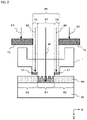
- the template 1 has a first step structure 21 on a main surface 11 of a base 10 , has a second step structure 22 on the first step structure 21 , and has a transfer pattern 23 on an upper surface of the second step structure 22 , and an outer side region of the second step structure 22 at an upper surface of the first step structure 21 is covered with a light shielding film 31 .
- the upper surface of the second step structure 22 becomes the transfer pattern region.
- the template 1 it is possible to suppress the influence of leakage of exposure light (irradiation to an unintended region) during the imprinting while maintaining the required height (the distance from the main surface 11 of the base 10 ) of the transfer pattern region.
- the height (the distance from the main surface 11 of the base 10 ) of the transfer pattern region can be maintained at a required height.
- the template 1 has the light shielding film 31 on the upper surface of the first step structure 21 , in comparison with a form (for example, FIG. 7C in Patent Document 5) in which a light shielding member is provided only on the main surface 11 of the base 10 as in the related art, the light shielding film 31 exists at a distance closer to the upper surface of the second step structure 22 which is the transfer pattern region in the vertical direction (the Z direction in the figure). Therefore, it is possible to suppress the influence of leakage of exposure light (irradiation to an unintended region) during the imprinting.
- FIG. 2 is a diagram illustrating a usage example of the template according to the first embodiment.
- the exposure light for example, ultraviolet light having a wavelength of 365 nm
- the exposure light for example, ultraviolet light having a wavelength of 365 nm
- a frame-shaped light shielding plate in a planar view in which the exposure region is an opening is provided.
- the region irradiated with the exposure light is defined in the irradiation region 90 corresponding to the opening of the light shielding plate 70 .
- the exposure light 83 outside the irradiation region 90 is shielded by the light shielding plate 70 and is not emitted onto the photocurable resin 60 .
- the irradiation region 90 defined by the light shielding plate 70 is usually designed to be larger than the transfer region 61 of the photocurable resin 60 . That is, as illustrated in FIG. 2 , the irradiation region 90 includes not only an irradiation region 91 having a size corresponding to the transfer region 61 of the photocurable resin 60 but also an unnecessary irradiation region 92 .
- the exposure light 82 in the irradiation region 92 is shielded by the light shielding film 31 formed on the upper surface of the first step structure 21 .
- the exposure light 81 of the irradiation region 91 having a size corresponding to the transfer region 61 is emitted onto the photocurable resin 60 on the transfer substrate 50 .
- the light shielding film 31 formed on the upper surface of the first step structure 21 is not necessarily formed so as to cover the entire region from the part (that is, the outer edge of the bottom of the second step structure 22 ) where the second step structure 22 and the upper surface of the first step structure 21 are in contact with each other to the outer edge of the upper surface of the first step structure 21 but may be formed in the region necessary to shield the exposure light 82 .
- the light shielding film 31 formed on the upper surface of the first step structure 21 may be formed so as to cover at least the region from the part (that is, the outer edge of the bottom of the second step structure 22 ) where the second step structure 22 and the upper surface of the first step structure 21 are in contact with each other to the outer edge of the upper surface of the first step structure 21 in the region corresponding to the irradiation region 90 illustrated in FIG. 2 .
- the light shielding film 31 formed on the upper surface of the first step structure 21 covers the entire region from the part (that is, the outer edge of the bottom of the second step structure 22 ) where the second step structure 22 and the upper surface of the first step structure 21 are in contact with each other to the outer edge of the upper surface of the first step structure 21 , even though the shape accuracy and the positional accuracy of the light shielding plate 70 illustrated in FIG. 2 are low, it is possible to more reliably prevent the photocurable resin 60 in the non-transfer region 62 from unintentionally being cured.
- FIGS. 3A and 3B are diagrams illustrating the function and effect of the template according to the first embodiment
- FIG. 3A is a schematic cross-sectional diagram of the template according to the first embodiment
- FIG. 3B is a schematic enlarged diagram illustrating the leakage state of the exposure light L 1 in the region R 2 illustrated in FIG. 3A
- FIGS. 12A and 12B are diagrams illustrating problems of the template in the related art
- FIG. 12A is a schematic cross-sectional diagram of the template in the related art
- FIG. 12B is a schematic enlarged diagram illustrating the leakage state of the exposure light L 2 in the region R 102 illustrated in FIG. 12A .
- the template 101 in the related art which has a step structure 121 on a main surface 111 of a base 110 and has a transfer pattern 122 on an upper surface of the step structure 121 and in which an outer side region of the step structure 121 at the main surface 111 of the base 110 is covered with alight shielding film 131 , the upper surface (transfer pattern region) of the step structure 121 and the main surface 111 (more precisely, the upper surface of the light shielding film 131 ) of the base 110 are separated by the distance H 101 .
- the distance H 101 is determined, for example, by the mechanical accuracy of the imprinting apparatus to be used. However, the distance is typically about 30 ⁇ m.
- the step structure 121 requiring about 30 ⁇ m in step difference (corresponding to approximately H 101 ) takes time to produce by dry etching, the step structure is usually formed by wet etching.
- the cross-sectional shape of the part where the step structure 121 and the main surface 111 of the base 110 are in contact with each other is hard to be a right angle, and the cross-sectional shape tends to be a rounded shape as illustrated in FIG. 12B .
- this rounded shape part (the part where the step structure 121 and the main surface 111 of the base 110 are in contact with each other), it is difficult to form the light shielding film 131 with the same thickness as the other parts, and thus, the exposure light easily leaks.
- the light shielding film 131 it is difficult to form the light shielding film 131 with the same thickness as other parts in the region corresponding to A 3 .
- the exposure light L 3 directed to the side surface of the step structure 121 is totally reflected, so that it can be considered that the problem that the photocurable resin 60 in the non-transfer region 62 is unintentionally cured by the exposure light L 3 does not occur in principle.
- the refractive index of synthetic quartz which is appropriately used as a material of a template at a wavelength of 365 nm is about 1.47 and the refractive index of air is assumed to be 1.0, the exposure light L 3 having an incident angle ⁇ of 43° or more is totally reflected, so that light is not emitted from the side surface of the step structure 121 .
- the template 1 according to the first embodiment which has the first step structure 21 on the main surface 11 of the base 10 , has the second step structure 22 on the first step structure 21 , and has the transfer pattern 23 on the upper surface of the second step structure 22 and which has a form where an outer side region of the second step structure 22 at an upper surface of the first step structure 21 is covered with the light shielding film 31 , the upper surface (more precisely, the bottom surface of the concave part of the transfer pattern 23 ) of the second step structure 22 and the upper surface (more precisely, the upper surface of the light shielding film 31 ) of the first step structure 21 are separated by a distance (H 2 ⁇ H 1 ).
- the combined height (H 2 ) of the step difference of the first step structure 21 and the step difference of the second step structure 22 serves as the height of about 30 ⁇ m, which is required, for example, depending on the mechanical precision of the imprinting apparatus to be used.
- the exposure light L 1 leaking from the part where the second step structure 22 and the upper surface of the first step structure 21 are in contact with each other spreads as diffracted light depending on the distance (H 2 ⁇ H 1 ).
- the distance (H 2 ⁇ H 1 ) can be made smaller than the distance H 101 (about 30 ⁇ m) illustrated in FIG. 12B , it is possible to suppress the spreading to be small.
- the region (corresponding to A 1 illustrated in FIG. 3B ) where the resin may be cured can also be formed to be smaller than the region corresponding to A 2 illustrated in FIG. 12B .
- the step difference in which the step difference is substantially (H 2 ⁇ H 1 ), for example, if the step difference is several ⁇ m or less, the step difference can be sufficiently formed in terms of time by dry etching.
- the cross-sectional shape of the part where the second step structure 22 and the upper surface of the first step structure 21 are in contact with each other can be formed at a right angle compared to a rounded shape illustrated in FIG. 12B .
- the light shielding film 31 with the same thickness as the other parts also in the part where the second step structure 22 and the upper surface of the first step structure 21 are in contact with each other, so that the leakage of the exposure light L 1 is easily suppressed.
- the first step structure 21 in which the step difference is substantially H 1 may be formed by wet etching as in the related art.
- the cross-sectional shape of the part where the first step structure 21 and the main surface 11 of the base 10 are in contact with each other tends to have a rounded shape.
- the light shielding film 31 formed on the upper surface of the second step structure 22 is responsible for shielding the exposure light, the effect of the light shielding film 31 is not impaired by the rounded shape.
- the value of the distance (H 2 ⁇ H 1 ) can be applied as long as the value of the distance is smaller than the height (typically about 30 ⁇ m) required, for example, depending on the mechanical accuracy of the imprinting apparatus to be used.
- a gap (space) is formed between the upper surface (the downward direction in FIG. 2 ) of the light shielding film 31 and the bottom surface (the same as the position of the upper surface of the photocurable resin 60 in FIG. 2 ) of the concave part of the transfer pattern 23 .
- the above-described distance (H 2 ⁇ H 1 ) can be set to be in a range of 1 ⁇ m or more and 5 ⁇ m or less.
- the distance in the vertical direction from the main surface 11 of the base 10 to the upper surface of the light shielding film 31 on the first step structure 21 is regarded as H 1
- the distance in the vertical direction from the main surface 11 of the base 10 to the upper surface of the second step structure 22 is regarded as H 3
- the distance in the horizontal direction from the outer edge of the main surface 11 of the base 10 to the outer edge of the upper surface of the first step structure 21 is regarded as D 1
- the distance in the horizontal direction from the outer edge of the main surface 11 of the base 10 to the outer edge of the upper surface of the second step structure 22 is regarded as D 2
- it is preferable that a relationship of H 1 ⁇ H 3 ⁇ (D 1 /D 2 ) is satisfied.
- FIG. 4 is a diagram illustrating the positional relationship of step structures of the template according to the first embodiment and corresponds to an enlarged diagram of main parts of R 1 indicated by a broken line circle in FIG. 1 .
- the outer edge E 2 of the light shielding film 31 on the first step structure 21 exists in an inner side (on the template 1 side) than the broken line connecting the outer edge E 1 of the main surface 11 of the base 10 and the outer edge E 3 of the upper surface of the second step structure 22 .
- a depression part 40 including the second step structure 22 in a planar view is provided on the surface (back surface 12 ) opposite to the main surface 11 of the base 10 . This is because a step such as releasing becomes easy.
- the depression part 40 includes the first step structure 21 in a planar view. This is because it is possible to prevent a problem that the light shielding film 31 formed on the upper surface of the first step structure 21 is peeled off during the bending.
- the inside of the depression part 40 is easily deformed during the bending because the thickness of the template 1 is small, whereas the outside of the depression part 40 is not easily deformed during the bending because the thickness of the template 1 is large.
- the first step structure 21 in a planar view, in a case where the first step structure 21 is not included in the depression part 40 , in other words, in a planar view, in a case where the first step structure 21 exists not only inside the depression part 40 but also outside the depression part 40 , the first step structure 21 has a boundary between the region (that is, inside the depression part 40 ) that is easily deformed and the region (that is, outside the depression part 40 ) that is not easily deformed.
- the light shielding film 31 formed on the upper surface of the first step structure 21 is peeled off, and thus, there is a concern that the boundary becomes the origin of defect.
- the main material constituting the template 1 that is, the material constituting the base 10 , the first step structure 21 , the second step structure 22 , and the transfer pattern 23 is a material that can be used for the photo imprinting method and can transmit exposure light during the imprinting.
- ultraviolet light having a wavelength in a range of 200 nm to 400 nm (in particular, in a range of 300 nm to 380 nm) is used as the exposure light.
- Examples of the above-mentioned material include transparent materials such as quartz glass, heat-resistant glass, calcium fluoride (CaF 2 ), magnesium fluoride (MgF 2 ), and acrylic glass and stacked structures of these transparent materials.
- transparent materials such as quartz glass, heat-resistant glass, calcium fluoride (CaF 2 ), magnesium fluoride (MgF 2 ), and acrylic glass and stacked structures of these transparent materials.
- synthetic quartz is suitable because the synthetic quartz has high rigidity, low thermal expansion coefficient, and high transmittance in a range of commonly used wavelength of 300 nm to 380 nm.
- the main material constituting the base and the main material constituting the step structure having the transfer pattern are the same material, and also in the template 1 , the first step structure 21 and the second step structure 22 having the transfer pattern 23 are made of the same material as the base 10 .
- a material constituting the light shielding film 31 for example, a material containing at least one of a metal material and oxide, nitride, and oxynitrides thereof can be used.
- a metal material which can be used include chromium (Cr), molybdenum (Mo), tantalum (Ta), tungsten (W), zirconium (Zr), and titanium (Ti).
- the light shielding film 31 has a transmittance of 10% or less at a wavelength of 365 nm.
- the thickness of the light shielding film 31 may be 15 nm or more.
- the transfer pattern of the template for imprinting according to the first embodiment may be a line-and-space pattern or a pillar shape.
- the line width is about 30 nm and the height thereof is about 60 nm.
- the diameter is about 50 nm, and the height thereof is about 60 nm.
- the width in the longitudinal direction and the width in the lateral direction of the first step structure 21 or the second step structure 22 are particularly limited as long as the widths satisfy the above-mentioned conditions, and the width in the longitudinal direction and the width in the lateral direction may be the same as each other or different from each other.
- FIG. 5 is a diagram illustrating a configuration example of the template according to the second embodiment.
- the template 1 has a first step structure 21 on the main surface 11 of the base 10 , has a second step structure 22 on the first step structure 21 , and has a transfer pattern 23 on the upper surface of the second step structure 22 , and an outer side region of the second step structure 22 at an upper surface of the first step structure 21 is covered with the light shielding film 31 .
- the template 1 has, on the upper surface of the second step structure 22 , a first concave and convex structure body 22 a constituting the transfer pattern 23 and a second concave and convex structure body 22 b constituting an alignment mark.
- a high contrast film 32 made of a material film different from the material constituting the base 10 is formed on the light shielding film 31 and on the bottom surface of the concave part of the second concave and convex structure body 22 b.
- the high contrast film 32 is formed on the lower side of the concave part of the second concave and convex structure body 22 b .
- the upper surface of the second concave and convex structure body 22 b becomes the transfer pattern region.
- the template 1 it is possible to suppress the influence of leakage of exposure light (irradiation to an unintended region) during the imprinting, while maintaining the required height (the distance from the main surface 11 of the base 10 ) of the transfer pattern region.
- the high contrast film 32 is formed on the bottom surface of the concave part of the second concave and convex structure body 22 b constituting the alignment mark, and the light shielding film 31 and the high contrast film 32 are sequentially stacked on the outer side region of the second step structure 22 at an upper surface of the first step structure 21 .
- the template 1 illustrated in FIG. 5 it is possible to satisfy both requirements of improving the contrast of the alignment mark during the position alignment and preventing light irradiation to an unintended region during the imprinting.
- the light shielding property of the stacked structure in which the light shielding film 31 and the high contrast film 32 are sequentially stacked is higher than the light shielding property of only the light shielding film 31 illustrated in FIG. 1 , for example, the exposure light 82 in the originally unnecessary irradiation region 92 illustrated in FIG. 2 can be more effectively shielded than that of the template 1 illustrated in FIG. 1 .
- a gap is formed between the upper surface of the high contrast film 32 formed on the light shielding film 31 and the bottom surface of the concave part of the transfer pattern 23 .
- the value of the distance (H 12 ⁇ H 11 ) between the bottom surface of the concave part of the transfer pattern 23 and the upper surface of the high contrast film 32 formed on the light shielding film 31 can be set to be in a range of 1 ⁇ m or more and 5 ⁇ m or less.
- the distance in the vertical direction from the main surface 11 of the base 10 to the upper surface of the high contrast film 32 formed on the light shielding film 31 is regarded as H 11
- the distance in the vertical direction from the main surface 11 of the base 10 to the upper surface of the second step structure 22 is regarded as H 13
- the distance in the horizontal direction from the outer edge of the main surface 11 of the base 10 to the outer edge of the upper surface of the first step structure 21 is regarded as D 11
- the distance in the horizontal direction from the outer edge of the main surface 11 of the base 10 to the outer edge of the upper surface of the second step structure 22 is regarded as D 12
- a depression part 40 including the second step structure 22 in a planar view is provided on the surface (back surface 12 ) opposite to the main surface 11 of the base 10 .
- the depression part 40 includes the first step structure 21 in a planar view.
- FIG. 6 is a diagram illustrating an example of the main parts of the template according to the second embodiment.
- the template for imprinting by forming a hard mask pattern which is to be an etching mask when forming the first concave and convex structure body 22 a and the second concave and convex structure body 22 b , after that, half-etching the second concave and convex structure body 22 b in a state where the hard mask pattern region for forming the first concave and convex structure body 22 a is covered with the resin layer, and after that, by removing the resin layer and forming the first concave and convex structure body 22 a and the second concave and convex structure body 22 by etching.
- the main material constituting the template 1 illustrated in FIG. 5 that is, the material constituting the base 10 , the first step structure 21 , and the second step structure 22 is similar to that of the template 1 illustrated in FIG. 1 , the description thereof will be omitted herein.
- the material constituting the first concave and convex structure body 22 a and the second concave and convex structure body 22 b in the template 1 illustrated in FIG. 5 is similar to the material constituting the transfer pattern 23 in the template 1 illustrated in FIG. 1 , the description thereof will be omitted herein.
- any material having light shielding properties can be used.
- the same material as the light shielding film 31 in the template 1 illustrated in FIG. 1 can be used.
- the light shielding film 31 has a transmittance of 10% or less at a wavelength of 365 nm.
- the thickness of the light shielding film 31 may be 15 nm or more.
- the thickness is preferably within a range of 35 nm to 1000 nm, particularly preferably within a range of 55 nm to 1000 nm. This is because the thickness of the light shielding film 31 is larger than these lower limits, so that the transmittance at a wavelength of 365 nm is 1% or less and the transmittance at a wavelength of 365 nm is 0.1% or less, and this is because the thickness of the light shielding film 31 is smaller than these upper limits, so that film peeling can be avoided.
- any material having a refractive index different from that of the material constituting the base 10 with respect to the alignment light and having a light shielding property can be used.
- the same material as the light shielding film 31 in the template 1 illustrated in FIG. 1 can be used.
- the thickness of the high contrast film 32 is not particularly limited as long as the thickness can satisfy the requirement of contrast of the alignment mark during the position alignment and the requirement of light shielding property, in the production method of the template for imprinting having a high contrast film described later, it is preferable to make the thickness as large as possible by forming the high contrast film 32 as thick as possible. This is because the contrast of the alignment mark is improved.
- the thickness of the high contrast film 32 cannot be greatly changed due to restrictions on the structure and manufacturing of the first concave and convex structure body 22 a and the second concave and convex structure body 22 b , the thickness of the light shielding film 31 can be greatly changed.
- FIG. 7 is a diagram illustrating a configuration example of the template blank according to the present invention.
- the template blank 2 has, on the main surface 11 of the base 10 , the first step structure 21 and the second step structure 22 on the first step structure 21 , and an outer side region of the second step structure 22 at an upper surface of the first step structure 21 is covered with a light shielding film 31 .
- the template blank 2 is a template blank of producing the template 1 .
- the template 1 as illustrated in FIG. 1 can be produced by forming the transfer pattern 23 having a concave and convex structure on the upper surface of the second step structure 22 of the template blank 2 .
- the template 1 it is possible to suppress the influence of leakage of exposure light (irradiation to an unintended region) during the imprinting while maintaining the required height of the transfer pattern region.
- the distance H 4 in the vertical direction from the main surface 11 of the base 10 to the upper surface of the second step structure 22 corresponds to the sum of the distance H 2 and the height of the convex part of the transfer pattern 23 in the template 1 illustrated in FIG. 1 .
- the distance H 4 illustrated in FIG. 7 can be treated as approximately the same value as the distance H 2 illustrated in FIG. 1 .
- the value of the distance (H 4 ⁇ H 1 ) in the template blank 2 illustrated in FIG. 7 can be applied as long as the value of the distance is smaller than the height (typically about 30 ⁇ m) required, for example, depending on the mechanical accuracy of the imprinting apparatus to be used.
- the smaller the value the more effective the value is.
- a gap (space) is formed between the upper surface (the downward direction in FIG. 2 ) of the light shielding film 31 and the bottom surface (the same as the position of the upper surface of the photocurable resin 60 in FIG. 2 ) of the concave part of the transfer pattern 23 .
- the above-described value of the distance (H 4 ⁇ H 1 ) can be set to be in a range of 1 ⁇ m or more and 5 ⁇ m or less.
- the distance in the vertical direction from the main surface 11 of the base 10 to the upper surface of the light shielding film 31 on the first step structure 21 is regarded as H 1
- the distance in the vertical direction from the main surface 11 of the base 10 to the upper surface of the second step structure 22 is regarded as H 4
- the distance in the horizontal direction from the outer edge of the main surface 11 of the base 10 to the outer edge of the upper surface of the first step structure 21 is regarded as D 1
- the distance in the horizontal direction from the outer edge of the main surface 11 of the base 10 to the outer edge of the upper surface of the second step structure 22 is regarded as D 2
- it is preferable that a relationship of H 1 ⁇ H 4 ⁇ (D 1 /D 2 ) is satisfied.
- FIG. 8 is a diagram illustrating the positional relationship of step structures of the template blank according to the present invention and corresponds to an enlarged diagram of main parts of R 3 illustrated by a broken line circle in FIG. 7 .
- the outer edge E 2 of the light shielding film 31 on the first step structure 21 exists in an inner side (on the template blank 2 side) than the broken line connecting the outer edge E 1 of the main surface 11 of the base 10 and the outer edge E 3 of the upper surface of the second step structure 22 .
- a depression part 40 including the second step structure 22 in a planar view is provided on a surface (back surface 12 ) opposite to the main surface 11 of the base 10 . This is because a step such as releasing of the template 1 becomes easy.
- the depression part 40 includes the first step structure 21 in a planar view. This is because it is possible to prevent a problem that the light shielding film 31 formed on the upper surface of the first step structure 21 is peeled off during the bending.
- the inside of the depression part 40 is a region that is easily deformed during the bending of the template 1 because the thickness of the template blank 2 is small, whereas the outside of the depression part 40 is a region that is not easily deformed during the bending of the template 1 since the thickness of the template blank 2 is large.
- the first step structure 21 in a planar view, in a case where the first step structure 21 is not included in the depression part 40 , in other words, in a planar view, in a case where the first step structure 21 exists not only inside the depression part 40 but also outside the depression part 40 , the first step structure 21 has a boundary between the region (that is, inside the depression part 40 ) that is easily deformed and the region (that is, outside the depression part 40 ) that is not easily deformed.
- the light shielding film 31 formed on the upper surface of the first step structure 21 is peeled off, and thus, there is a concern that the boundary becomes the original of defect.
- the same material as the above-described template 1 can be used.
- FIG. 9 is a flowchart illustrating an example of the production method of the template blank according to the present invention.
- FIGS. 10A to 10C and 11D to 11F are schematic process diagrams illustrating an example of the production method of the template blank according to the present invention.
- the template according to the present invention can be produced by forming the transfer pattern 23 on the upper surface of the second step structure 22 by the same method as the method in the related art using the template blank according to the present invention. Therefore, the description of the production method of the template according to the present invention with reference to the drawings will be omitted.
- a first template blank 200 having a mesa-shaped step structure 201 on the main surface 11 of the base 10 is prepared (S 1 in FIG. 9 , FIG. 10A ).
- first template blank 200 a template blank which does not have the first step structure 21 , the second step structure 22 , and the light shielding film 31 as in the template blank 2 , for example, a template blank which is the same as the template blank used for the photo imprinting method in the related art can be used.
- the first template blank 200 is made of, for example, synthetic quartz.
- the distance H 201 from the main surface 11 of the base 10 to the upper surface of the step structure 201 is approximately the same as the distance H 4 of the template blank 2 illustrated in FIG. 7 and is typically about 30 ⁇ m.
- a depression part 40 is provided on the back surface 12 side of the base 10 .
- a first etching mask 210 is formed on the upper surface of the step structure 201 (S 2 in FIG. 9 , FIG. 10B ).
- the first etching mask 210 can be formed by performing sputtering film formation using chromium (Cr) and, after that, performing a patterning process in a mask shape.
- Cr chromium
- the first step structure 21 and the second step structure 22 are formed by dry etching by using the first etching mask 210 as a mask (S 3 in FIG. 9 , FIG. 10C ).
- the etching gas for example, a fluorine-based gas can be used.
- the distance H 202 (corresponding to the etching depth) illustrated in FIG. 10C is about several ⁇ m (in a range of 1 ⁇ m or more and 5 ⁇ m or less).
- the first etching mask 210 is removed ( FIG. 11D ), and subsequently, the light shielding material layer 220 , which is to be the light shielding film 31 later, is formed on the main surface 11 of the base 10 , the upper surface of the first step structure 21 , and the upper surface of the second step structure 22 , and the second etching mask 230 is formed in the outer side region of the second step structure 22 at an upper surface of the first step structure 21 (S 4 and S 5 in FIG. 9 , FIG. 11E ).
- the light shielding material layer 220 can be formed by sputtering film formation using chromium (Cr) so that the thickness is 15 nm or more.
- the second etching mask 230 made of a resin can be formed by dropping a resin onto the outer side region of the second step structure 22 at an upper surface of the first step structure 21 .
- the template blank 2 which has the first step structure 21 on the main surface 11 of the base 10 and has the second step structure 22 on the first step structure 21 and in which the outer side region of the second step structure 22 at an upper surface of the first step structure 21 is covered with the light shielding film 31 is obtained (S 6 in FIG. 9 , FIG. 11F ).
- a production method of a template substrate for imprinting, a production method of a template for imprinting, and a template according to the present invention will be described in detail with reference to the drawings.
- the template substrate for imprinting and the template for imprinting are appropriately simply referred to as a template substrate and a template, respectively.
- FIG. 13 is a diagram illustrating an example of the template substrate according to the present invention.
- FIG. 14 is a diagram illustrating an example of the template according to the present invention.
- the template substrate 4 has a first step structure 21 on a main surface 11 of a base 10 and has a second step structure 22 on the first step structure 21 , and an outer side region of the second step structure 22 at an upper surface (exposed table, terrace) of the first step structure 21 is covered with a light shielding film 31 .
- the template substrate 4 is a template substrate of producing a template 1 having the light shielding film 31 as illustrated in FIG. 14 , and it is possible to produce the template 1 as illustrated in FIG. 14 , for example, by forming a transfer pattern in a concave and convex structure on the upper surface of the second step structure 22 of the template substrate 4 .
- the upper surface of the second step structure 22 becomes the transfer pattern region.
- the template 1 it is possible to suppress the influence of leakage of exposure light (irradiation to an unintended region) during the imprinting while maintaining the required height of the transfer pattern region.
- the height (the distance from the main surface 11 of the base 10 ) of the transfer pattern region can be maintained at a required height (for example, 30 ⁇ m).
- the template 1 has the light shielding film 31 on the upper surface of the first step structure 21 , in comparison with a form (for example, FIG. 7C in Patent Document 5) in which a light shielding member is provided only on the main surface 11 of the base 10 as in the related art, the light shielding film 31 exists at a distance closer to the upper surface of the second step structure 22 which is the transfer pattern region in the vertical direction (the Z direction in the figure). Therefore, it is possible to suppress the influence of leakage of exposure light (irradiation to an unintended region) during the imprinting.
- the value of the step difference (H 1 ) of the second step structure 22 can be set to be in a range of 1 ⁇ m or more and 5 ⁇ m or less. If the step difference is several ⁇ m or less, the step difference can be sufficiently formed in terms of time by dry etching.
- the cross-sectional shape of the part where the second step structure 22 and the upper surface of the first step structure 21 are in contact with each other can be formed at a right angle compared to the case of formation by wet etching.
- the light shielding film 31 with the same thickness as the other parts also in the part where the second step structure 22 and the upper surface of the first step structure 21 are in contact with each other, so that the leakage of the exposure light L 1 is easily suppressed.
- FIG. 15 is a flowchart illustrating an example of the production method of the template substrate for imprinting according to the present invention.
- FIG. 16 is a flowchart illustrating an example of a resin layer forming step according to the present invention.
- FIGS. 17A to 17C and 18D to 18F are schematic process diagrams illustrating an example of the production method of the template substrate for imprinting according to the present invention.
- the production method of the template substrate for imprinting according to the present invention is a production method of a template substrate for imprinting having a first step structure on a main surface of a base, having a second step structure on the first step structure, and having a light shielding film on an upper surface of the first step structure, and as illustrated in FIG.
- the resin layer forming step (S 20 ) includes a resin thickness specifying step (S 21 in FIG. 16 ) of, by using a template for specifying resin thickness having a concave part having a rectangular shape in a planar view on the main surface side in contact with the resin, pressing the upper surface of the outer peripheral part of the concave part of the template for specifying resin thickness against the first resin dropped onto the light shielding material layer formed on the upper surface of the first step structure, and pressing the bottom surface of the concave part of the template for specifying resin thickness against the second resin dropped onto the light shielding material layer formed on the upper surface of the second step structure, and the depth of the concave part of the template for specifying resin thickness is smaller than the height from the upper surface of the first step structure to the upper surface of the second step structure.
- a multistep template substrate 300 with a light shielding material layer which has the first step structure 21 and the second step structure 22 and has a light shielding material layer 170 on the upper surface (exposed table, terrace) of the first step structure 21 and on the upper surface of the second step structure 22 is prepared (S 10 in FIG. 15 , FIG. 17A ).
- the combined height of the first step structure 21 and the second step structure 22 is a height which is the same as or similar to the step difference of the template substrate having a one step structure used in the photo imprinting method in the related art and is typically about 30 ⁇ m.
- a depression part 40 is provided on the back surface 12 side of the base 10 .
- the multistep template substrate 300 with the light shielding material layer can be produced from a template substrate having a one step structure used in a photo imprinting method in the related art.
- the production method of the multistep template substrate with the light shielding material layer will be described later in detail.
- the thickness of the second resin layer 52 can be formed so as to be smaller than the thickness of the first resin layer 51 .
- the first resin layer 51 can be formed as a resin layer having a uniform thickness.
- the height difference of the thickness of the first resin layer 51 can be set to be 50 nm or less.
- the second resin layer 52 is removed while allowing the first resin layer 51 to remain.
- the second resin layer 52 is smaller than the thickness of the first resin layer 51 , by the etch-back method, the second resin layer 52 can be removed while allowing the first resin layer 51 to remain.
- oxygen gas can be used as the etching gas 75 .
- the light shielding material layer 170 exposed from the first resin layer 51 is etched, so that the light shielding material layer 170 formed on the upper surface of the second step structure 22 is removed while allowing the light shielding material layer 170 formed on the upper surface of the first step structure 21 to remain.
- the light shielding material layer 170 formed on the upper surface of the first step structure 21 remaining in this step becomes the light shielding film 31 of the template substrate 4 .
- any one of dry etching and wet etching can be used for this etching.
- the dry etching by using a mixed gas of oxygen and chlorine can be used.
- the wet etching by using an aqueous solution containing ceric ammonium nitrate and perchloric acid can be used.
- the template substrate 4 having the first step structure 21 on the main surface 11 of the base 10 , having the second step structure 22 on the first step structure 21 , and having the light shielding film 31 on the upper surface (exposed table, terrace) of the first step structure 21 can be obtained.
- ashing by using oxygen gas can be used.
- the second resin 52 a is not dropped onto the light shielding material layer 170 formed on the upper surface of the second step structure 22 (that is, the resin layer is not formed on the light shielding material layer 170 formed on the upper surface of the second step structure 22 ) and the light shielding material layer 170 formed on the upper surface of the second step structure 22 is to be removed by etching
- the formed resin layer has a defective part (a part without resin) or a thin film part (a part with a thin resin) according to the density distribution of the dropped first resin 51 a . Then, if dry etching (etch-back) illustrated in FIG. 18E is performed, such a defective part and a thin film part are further increased.
- the light shielding material layer 170 is etched in a subsequent step, the light shielding material layer 170 formed on the upper surface of the first step structure 21 which is to be the light shielding film 31 also has a defective part or a thin film part.
- the thickness of the second resin layer 52 for example, including splashes when the first resin 51 a is dropped can be formed to be smaller than the thickness of the first resin layer 51 .
- both the first resin layer 51 and the second resin layer 52 can be formed as a resin layer having a uniform thickness.
- the second resin layer 52 can be removed while allowing the first resin layer 51 to remain.
- the light shielding material layer 170 exposed from the first resin layer 51 is etched, so that as illustrated in FIG. 18F , on the upper surface of the second step structure 22 , the light shielding material layer 170 can be removed without allowing the light shielding material layer 170 to remain.
- the first resin layer 51 can be formed as a resin layer having a uniform thickness without a defective part
- the light shielding material layer 170 formed on the upper surface of the first step structure 21 which is to be the light shielding film 31 can also be a film without a defective part or a thin film part.
- the first resin 51 a and the second resin 52 a are made of a material that is cured by heat or light and are preferably ultraviolet curable resins used in the field of nanoimprint lithography.
- first resin 51 a and the second resin 52 a are ultraviolet curable resins
- a method of irradiating with the ultraviolet light 65 can be used.
- the first resin 51 a and the second resin 52 a may be made of different materials as long as the second resin layer 52 can be removed by dry etching in the second resin layer removing step described later (S 30 in FIG. 15 , FIG. 18E ) while allowing the first resin layer 51 to remain.
- these resins are made of the same material.
- FIGS. 19A and 19B are diagrams illustrating an example of the template for specifying resin thickness according to the present invention.
- FIG. 19A illustrates a schematic bottom diagram of the template 400 for thickness regulation of the resin
- FIG. 19B illustrates a cross sectional diagram taken along line A-A in FIG. 19A .
- the template 400 for thickness regulation of the resin illustrated in FIGS. 19A and 19B has a concave part 402 on the main surface side (lower side in FIG. 19B ) which is in contact with resin, and the concave part 402 is surrounded by a frame-shaped convex part 403 in a planar view. That is, in the template 400 for thickness regulation of the resin, the upper surface of the outer peripheral part of the concave part 402 corresponds to the upper surface of the frame-shaped convex part 403 in a planar view.
- the concave part 402 of the template 400 for thickness regulation of the resin has a size of enclosing the upper surface of the second step structure 22 of the multistep template substrate 300 with the light shielding material layer and being enclosed in a region surrounded by the outer edge of the upper surface of the first step structure 21 of the multistep template substrate 300 with the light shielding material layer, and the depth of the concave part 402 of the template 400 for thickness regulation of the resin is set to be smaller than the height from the upper surface of the first step structure 21 to the upper surface of the second step structure 22 of the multistep template substrate 300 with the light shielding material layer.
- FIG. 20 is a diagram illustrating the function and effect of the template for specifying resin thickness according to the present invention.
- FIG. 20 corresponds to an enlarged diagram of the main parts in FIG. 17C .
- the depth (the same as the height of the convex part 403 in the template 400 for thickness regulation of the resin illustrated in FIG.
- the thickness of the first resin layer 51 to be formed is regarded as T 1
- the thickness of the second resin layer 52 to be formed is regarded as T 2 , by designing so that H 2 ⁇ H 1 , a relationship of T 2 ⁇ T 1 is obtained.
- the depth H 2 of the concave part 402 may be in a range of 0.3 ⁇ m or more and 10 ⁇ m or less.
- the thickness of the second resin layer 52 can be formed so as to be smaller than the thickness of the first resin layer 51 .
- the first resin layer 51 can be formed as a resin layer having a uniform thickness.
- the light shielding material layer 170 can be removed without allowing the light shielding material layer 170 to remain, and the light shielding material layer 170 formed on the upper surface of the first step structure 21 which is to be the light shielding film 31 can be a film without a defective part or a thin film part.
- the bottom surface of the concave part 402 of the template 400 for thickness regulation of the resin has a size of enclosing the upper surface (the same as the upper surface of the second step structure 22 of the template substrate 4 for imprinting) of the second step structure 22 of the multistep template substrate 300 with the light shielding material layer.
- the width of the bottom surface of the concave part 402 of the template 400 for thickness regulation of the resin illustrated in FIG. 19B is regarded as L 21 and the width of the upper surface of the second step structure 22 of the template substrate 4 for imprinting illustrated in FIG. 13 is regarded as L 11 , it is preferable that a relationship of L 21 >L 11 is satisfied.
- a bottom surface size of the concave part 402 may be set to be in a range of 10 mm ⁇ 10 mm or more and 70 mm ⁇ 70 mm or less.
- the region surrounded by the outer edge of the upper surface of the outer peripheral part of the concave part 402 of the template 400 for thickness regulation of the resin has the same shape and the same area as the region surrounded by the outer edge of the upper surface (the same as the upper surface of the first step structure 21 of the template substrate for imprinting) of the first step structure 21 of the multistep template substrate 300 with the light shielding material layer or has a size of enclosing the region surrounded by the outer edge of the upper surface (the same as the upper surface of the first step structure 21 of the template substrate for imprinting) of the first step structure 21 of the multistep template substrate 300 with the light shielding material layer.
- the width of the region surrounded by the outer edge of the upper surface of the convex part 403 of the template 400 for thickness regulation of the resin illustrated in FIG. 19B is regarded as L 22 and the width of the region surrounded by the outer edge of the upper surface of the first step structure 21 of the template substrate 4 for imprinting illustrated in FIG. 13 is regarded as L 12 , it is preferable that a relationship of L 22 ⁇ L 12 is satisfied.
- the first resin layer 51 can be formed as a resin layer having a uniform thickness without a defective part to the extent of reaching the outer edge of the upper surface (the same as the upper surface of the first step structure 21 of the template substrate 4 for imprinting) of the first step structure 21 of the multistep template substrate 300 with the light shielding material layer.
- the template 400 for thickness regulation of the resin has a region 404 having the same depth as the concave part 402 on the outer peripheral side of the convex part 403 .
- the measurement light is shielded by the convex part 403 and the multistep template substrate 300 with the light shielding material layer.
- the template 400 for thickness regulation of the resin has the region 404 as described above, when pressing the template 400 for thickness regulation of the resin, for example, the measurement light is not shielded by the convex part 403 and the multistep template substrate 300 with the light shielding material, and it is possible to measure the position of the height of the region 404 . Therefore, from this measurement result, the position of the height of the concave part 402 can be grasped.
- the template 400 for thickness regulation of the resin has marks for position matching on the main surface side.
- FIGS. 21A and 21B are diagrams illustrating another example of the template for specifying resin thickness according to the present invention.
- the template 410 for thickness regulation of the resin illustrated in FIG. 21A has a depression part 415 including the concave part 412 in a planar view on the surface opposite to the main surface side.
- this is because it is possible to facilitate bending by reducing the thickness of the region where the concave part 412 of the template 410 for thickness regulation of the resin is provided, it is possible to further exclude mixing of air bubbles during the pressing, and it is possible to perform partially releasing sequentially from the outer edge part of the concave part 412 during the releasing.
- the template for specifying resin thickness according to the present invention may be a form in which the outer edge of the upper surface of the outer peripheral part of the concave part 422 reaches the outer edge of the template for specifying resin thickness as in the template 420 for thickness regulation of the resin illustrated in FIG. 21B .
- the thickness of the second resin layer 52 can be formed so as to be smaller than the thickness of the first resin layer 51 .
- the first resin layer 51 can also be formed as a resin layer having a uniform thickness.
- a depression part including the concave part 422 may be provided on the surface opposite to the main surface side in a planar view.
- this is because it is possible to facilitate bending by reducing the thickness of the region where the concave part 422 of the template 420 for thickness regulation of the resin is provided, it is possible to further exclude mixing of air bubbles during the pressing, and it is possible to perform partially releasing sequentially from the outer edge part of the concave part 422 during the releasing.
- FIG. 22 is a flowchart illustrating an example of the production method of the multistep template substrate with the light shielding material layer according to the present invention.
- FIGS. 23A to 23C and 24D to 24E are schematic process diagrams illustrating an example of the production method of the multistep template substrate with the light shielding material layer according to the present invention.
- the production method of the multistep template substrate with the light shielding material layer includes, in order, a one step template substrate preparing step (S 11 in FIG. 22 ) of preparing a one step template substrate having a one step structure on a main surface of a base, an etching mask forming step (S 12 in FIG. 22 ) of forming an etching mask in a region which is to be a transfer pattern region of an upper surface of the step structure of the one step template substrate, a multistep forming step (S 13 in FIG. 22 ) of forming a first step structure of the lower step and a second step structure of the upper step by etching the step structure by using the etching mask, and a light shielding material layer forming step (S 14 in FIG. 22 ) of forming a light shielding material layer on an upper surface of the first step structure and on an upper surface of the second step structure.
- a one step template substrate 150 having a one step structure 151 is prepared on the main surface 11 of the base 10 ( FIG. 23A ).
- the material constituting the one step template substrate 150 is a material that can be used for the photo imprinting method and can transmit exposure light during the imprinting.
- ultraviolet light having a wavelength in a range of 200 nm to 400 nm (in particular, in a range of 300 nm to 380 nm) is used as the exposure light.
- Examples of the above-mentioned material include transparent materials such as quartz glass, heat-resistant glass, calcium fluoride (CaF 2 ), magnesium fluoride (MgF 2 ), and acrylic glass and stacked structures of these transparent materials.
- transparent materials such as quartz glass, heat-resistant glass, calcium fluoride (CaF 2 ), magnesium fluoride (MgF 2 ), and acrylic glass and stacked structures of these transparent materials.
- synthetic quartz is suitable because the synthetic quartz has high rigidity, low thermal expansion coefficient, and high transmittance in a range of commonly used wavelength of 300 nm to 380 nm.
- the height H 101 of the step structure 151 is a height which is the same as or similar to the step difference of the template substrate having a one step structure used in the photo imprinting method in the related art and is typically about 30 m.
- a depression part 40 is provided on the side of the back surface 12 of the base 10 of the one step template substrate 150 .
- an etching mask 160 is formed in a region which is to be a transfer pattern region on the upper surface of the step structure 151 of the one step template substrate 150 ( FIG. 23B ).
- region which is to be a transfer pattern region denotes a region where the transfer pattern 23 is formed in a template 1 for imprinting finally produced ( FIG. 14 ) through a multistep template substrate 300 with the light shielding material layer produced from the one step template substrate 150 .
- the upper surface of the second step structure 22 corresponds to a transfer pattern region.
- any material can be used as long as the material serves as an etching mask in dry etching the material constituting the one step template substrate 150 in the following multistep forming step.
- a metal material and one containing at least one of oxide, nitride, and oxynitride thereof can be used.
- Specific examples of the above-mentioned metal material which can be used include chromium (Cr), molybdenum (Mo), tantalum (Ta), tungsten (W), zirconium (Zr), and titanium (Ti).
- a chromium (Cr) film having a thickness of 30 nm or more and 200 nm or less by sputtering film formation, applying a photoresist, performing pattering, and after that, etching the chromium (Cr) film exposed from the photoresist, a desired etching mask 160 can be formed.
- etching the chromium (Cr) film for example, dry etching with a mixed gas of oxygen and chlorine can be used.
- the step structure 151 is etched by using the etching mask 160 as a mask to form the first step structure 21 of the lower step and the second step structure 22 of the upper step ( FIG. 23C ), and after that, the etching mask 160 is removed ( FIG. 24D ).
- the value of the step difference (H 102 ) of the second step structure 22 illustrated in FIG. 23C is the same as the value of the step difference (H 1 ) of the second step structure 22 of the template substrate 4 illustrated in FIG. 13 and can be set to be in a range of 1 ⁇ m or more and 5 ⁇ m or less. If the step difference is several ⁇ m or less, the step difference can be sufficiently formed in terms of time by dry etching.
- the cross-sectional shape of the part where the second step structure 22 and the upper surface of the first step structure 21 are in contact with each other can be formed at a right angle compared to the case of formation by wet etching.
- the material constituting the one step template substrate 150 is generally synthetic quartz, and dry etching by using a fluorine-based gas can be appropriately used for the etching.
- removal of the etching mask 160 can be performed by dry etching by using a mixed gas of oxygen and chlorine.
- removal of the etching mask may be performed by wet etching by using an aqueous solution containing ceric ammonium nitrate and perchloric acid.
- a light shielding material layer 170 is formed on the upper surface of the first step structure 21 and on the upper surface of the second step structure 22 to obtain a multistep template substrate 300 with the light shielding material layer ( FIG. 24E ).
- the light shielding material layer 170 is also formed on the main surface 11 of the base 10 .
- the light shielding material layer 170 on the main surface 11 is usually removed in the steps of FIGS. 18E to 18F .
- a material constituting the light shielding material layer 170 for example, a material containing at least one of a metal material and oxide, nitride, and oxynitride thereof can be used.
- a metal material which can be used include chromium (Cr), molybdenum (Mo), tantalum (Ta), tungsten (W), zirconium (Zr), and titanium (Ti).
- the light shielding material layer 170 has a transmittance of 10% or less at a wavelength of 365 nm.
- the thickness of the light shielding material layer 170 may be 15 nm or more.
- sputtering film formation which has been proven in the production of a photomask, for example, can be appropriately exemplified.
- the production method of a template for imprinting according to the present invention is substantially divided into a first embodiment and a second embodiment.
- first embodiment and the second embodiment will be described.
- a method of forming the desired transfer pattern 23 having a concave and convex structure by preparing the template substrate 4 produced by the production method of the template substrate for imprinting and performing the same step on the upper surface of the second step structure 22 as the production method of the template for imprinting in the related art as illustrated in FIG. 13 can be exemplified.
- the above-described methods of producing the template for imprinting in the related art include a method of forming resist patterns of the transfer pattern 23 , for example, by using an electron beam lithography technique and a method of forming resin patterns of the transfer pattern 23 by using an imprinting technique.
- the template 1 having the first step structure 21 on the main surface of the base 10 , having the second step structure 22 on the first step structure 21 , having the light shielding film 31 on the upper surface of the first step structure 21 , and having the transfer pattern 23 of the concave and convex structure on the upper surface of the second step structure 22 is produced.
- the above-described multistep template 700 with the light shielding material layer can be produced, for example, by preparing a template having the same configuration as the template in the related art, that is, a one step template 500 having a one step structure on the main surface of the base and having a transfer pattern 23 of a concave and convex structure on the upper surface of the step structure and performing the same steps as the production method of the multistep template substrate with the light shielding material layer according to the present invention (the first embodiment described later).
- the production method of the multistep template with the light shielding material layer according to the second embodiment will be described.
- the method (the production method of the template for imprinting according to the second embodiment) of producing the template for imprinting according to the present invention from the multistep template with the light shielding material layer will be described.
- the method (the production method of the template for imprinting according to the second embodiment) of producing the template for imprinting having the high contrast film according to the present invention from the multistep template with the light shielding material layer will be described.
- the production method of the multistep template with the light shielding material layer according to the second embodiment is substantially divided into the first embodiment and the second embodiment.
- the first embodiment and the second embodiment will be described.
- FIG. 25 is a flowchart illustrating an example of the production method of the multistep template with the light shielding material layer according to the first embodiment.
- FIGS. 26A to 26C and 27D to 27E are schematic process diagrams illustrating the example of the production method of the multistep template with the light shielding material layer according to the first embodiment.
- a one step template 500 having a one step structure 501 on the main surface 11 of the base 10 and having a transfer pattern 23 with a concave and convex structure on the upper surface of the step structure 501 is prepared (S 111 in FIG. 25 , FIG. 26A ).
- This one step template 500 is made of the same material as the template for imprinting in the related art.
- the one step template 500 has a configuration similar to that of the template for imprinting in the related art, and for example, the height H 501 of the step structure 501 is a height which is the same as or similar to the step difference of the template having a one step structure used in the photo imprinting method in the related art and is typically about 30 ⁇ m.
- a depression part 40 is provided on the back surface 12 side of the base 10 of the one step template 500 .
- the upper surface of the step structure 501 of the one step template 500 has an area larger than the upper surface of the second step structure 22 of the finally obtained template 1 .
- the upper surface of the step structure 501 of the one step template 500 is wider than the transfer pattern region (equal to the upper surface of the second step structure 22 of the template 1 ) in the template 1 , and the transfer pattern 23 formed in the one step template 500 is formed in a region which is to be the transfer pattern region in the template 1 .
- an etching mask 160 is formed in a region which is to be a transfer pattern region on the upper surface of the step structure 501 of the one step template 500 (S 112 in FIG. 25 , FIG. 26B ).
- the step structure 501 is etched by using the etching mask 160 to form the first step structure 21 of the lower step and the second step structure 22 of the upper step, and after that, the etching mask 160 is removed (S 113 in FIG. 25 , FIG. 26C , FIG. 27D ).
- the value of the step difference (H 502 ) of the second step structure 22 illustrated in FIG. 26C is the same as the value of the step difference (H 1 ) of the second step structure 22 of the template 1 illustrated in FIG. 14 and can be set in a range of 1 ⁇ m or more and 5 ⁇ m or less. If the step difference is several ⁇ m or less, the step difference can be sufficiently formed in terms of time by dry etching.
- the cross-sectional shape of the part where the second step structure 22 and the upper surface of the first step structure 21 are in contact with each other can be formed at a right angle compared to the case of formation by wet etching.
- a light shielding material layer 170 is formed on the upper surface of the first step structure 21 and on the upper surface of the second step structure 22 to obtain a multistep template 700 with the light shielding material layer (S 114 in FIG. 25 , FIG. 27E ).
- the light shielding material layer 170 is also formed on the main surface 11 of the base 10 , but in the production method of the template for imprinting according to the present invention, the light shielding material layer 170 on the main surface 11 is usually removed.
- FIG. 28 is a flow chart illustrating another example of the production method of the multistep template with the light shielding material layer according to the second embodiment.
- FIGS. 29A to 29C and 30D to 30F are schematic process diagrams illustrating another example of the production method of the multistep template with the light shielding material layer according to the second embodiment.
- a one step template substrate 150 having a one step structure 151 on the main surface 11 of the base 10 is prepared (S 211 in FIG. 28 , FIG. 29A ).
- the material constituting the one step template substrate 150 illustrated in FIG. 29A is similar to that of the one step template substrate 150 illustrated in FIG. 23 , the description thereof will be omitted herein.
- a depression part 40 is provided on the back surface 12 side of the base 10 of the one step template substrate 150 illustrated in FIG. 29A .
- an etching mask 160 is formed in a region which is to be the first concave and convex structure body constituting the transfer pattern on the upper surface of the step structure 151 of the one step template substrate 150 and the second concave and convex structure body constituting the alignment mark (S 212 in FIG. 28 , FIG. 29B ).
- the above “a region which is to be the first concave and convex structure body constituting the transfer pattern and the second concave and convex structure body constituting the alignment mark” denotes a region where the first concave and convex structure body 22 a and the second concave and convex structure body 22 b are formed in the template 1 for imprinting ( FIG. 38L ) finally produced through the multistep template 700 ( FIG. 30F ) with the light shielding material layer produced from the one step template substrate 150 .
- the material constituting the etching mask 160 is similar to the material constituting the etching mask 160 illustrated in FIG. 23B , the description thereof will be omitted herein.
- the step structure 151 is etched by using the etching mask 160 as a mask to form the first step structure 21 of the lower step and the second step structure 22 of the upper step, and after that, the etching mask 160 is removed (S 213 in FIG. 28 , FIG. 29C , FIG. 30D ).
- the value of the step difference (H 202 ) of the second step structure 22 illustrated in FIG. 29( c ) is the same as the value of the step difference (H 1 ) of the second step structure 22 of the template 1 illustrated in FIG. 14 and can be set in a range of 1 ⁇ m or more and 5 ⁇ m or less. If the step difference is several ⁇ m or less, the step difference can be sufficiently formed in terms of time by dry etching.
- the cross-sectional shape of the part where the second step structure 22 and the upper surface of the first step structure 21 are in contact with each other can be formed at a right angle compared to the case of formation by wet etching.
- a first concave and convex structure body 22 a constituting the transfer pattern 23 and a second concave and convex structure body 22 b constituting the alignment mark are formed on the upper surface of the second step structure 22 to obtain a multistep template 600 (S 214 in FIG. 28 , FIG. 30E ).
- a method of forming the first concave and convex structure body 22 a and the second concave and convex structure body 22 b a method of forming the desired first concave and convex structure body 22 a and the desired second concave and convex structure body 22 b by performing the same step as the production method of the template for imprinting in the related art can be exemplified.
- the above-described methods of producing the template for imprinting in the related art include a method of forming resist patterns of the first concave and convex structure body 22 a and the second concave and convex structure body 22 b , for example, by using an electron beam lithography technique and a method of forming resin patterns of the first concave and convex structure body 22 a and the second concave and convex structure body 22 b by using an imprinting technique.
- a light shielding material layer 170 is formed on the main surface 11 of the base 10 , on the upper surface of the first step structure 21 , and on the upper surface of the second step structure 22 to form a multistep template 700 with the light shielding material layer (S 215 in FIG. 28 , FIG. 30F ).
- the light shielding material layer 170 is also formed on the main surface 11 of the base 10 .
- the light shielding material layer 170 on the main surface 11 is usually removed.
- the material constituting the light shielding material layer 170 is similar to the material constituting the light shielding film 31 in the template 1 illustrated in FIG. 5 , the description thereof will be omitted herein. Since the thickness of the light shielding material layer 170 is similar to the thickness constituting the light shielding film 31 in the template 1 illustrated in FIG. 5 , the description thereof will be omitted herein.
- any one of the first embodiment as illustrated in FIGS. 25, 26A to 26C, and 27D to 27F , and the second embodiment as illustrated in FIGS. 28, 29A to 29C, and 30D to 30F may be employed, but the second embodiment is more preferable than the first embodiment.
- the second embodiment is because, in the step of forming the transfer pattern after the step of the multistep formation, the formation of the concave and convex structure body on the upper surface of the second step structure 22 , which is finer than the multistep formation, is performed, so that the risk of damage and destruction of the concave and convex structure body is reduced.
- FIG. 31 is a flowchart illustrating an example of the production method of the template according to the second embodiment.
- FIGS. 32A to 32C and 33D to 33F are schematic process diagrams illustrating the example of the production method of the template according to the second embodiment.
- a multistep template 700 with a light shielding material layer having a first step structure 21 and a second step structure 22 , having a transfer pattern 23 of a concave and convex structure on an upper surface of the second step structure 22 , and having the light shielding material layer 170 on an upper surface of the first step structure 21 and on the upper surface of the second step structure 22 is prepared (S 100 in FIG. 31 , FIG. 32A ).
- the combined height of the first step structure 21 and the second step structure 22 is a height which is the same as or similar to the step difference of the template substrate having a one step structure used in the photo imprinting method in the related art and is typically about 30 ⁇ m.
- a depression part 40 is provided on the back surface 12 side of the base 10 .
- the multistep template 700 with the light shielding material layer can be produced, for example, by the method ( FIGS. 25 to 27E ) of producing the multistep template with the light shielding material layer according to the first embodiment.
- the thickness of the second resin layer 52 can be formed to be smaller than the thickness of the first resin layer 51 by using the template 400 for thickness regulation of the resin having a predetermined form.
- the first resin layer 51 can be formed as a resin layer having a uniform thickness.
- the second resin layer 52 is removed while allowing the first resin layer 51 to remain by dry etching (etch-back) by using the etching gas 75 .
- the second resin layer 52 is smaller than the thickness of the first resin layer 51 , by the etch-back method, the second resin layer 52 can be removed while allowing the first resin layer 51 to remain.
- the light shielding material layer 170 formed on the upper surface of the second step structure 22 is removed while allowing the light shielding material layer 170 formed on the upper surface of the first step structure 21 to remain, which is to be a light shielding film 31 .
- the template 1 having the first step structure 21 on the main surface 11 of the base 10 , having the second step structure 22 on the first step structure 21 , having the transfer pattern 23 of the concave and convex structure on the upper surface of the second step structure 22 , and having the light shielding film 31 on the upper surface of the first step structure 21 can be obtained.
- FIG. 34 is a flowchart illustrating another example of the production method of the template according to the second embodiment.
- FIGS. 35A to 35C, 36D to 36F, 37G to 37I, and 38J to 38L are schematic process diagrams illustrating another example of the production method of the template according to the second embodiment.
- the combined height of the first step structure 21 and the second step structure 22 is a height which is the same as or similar to the step difference of the template substrate having a one step structure used in the photo imprinting method in the related art and is typically about 30 ⁇ m.
- a depression part 40 is provided on the back surface 12 side of the base 10 .
- the multistep template 700 with the light shielding material layer can be produced by, for example, the production method of the multistep template with the light shielding material layer according to the second embodiment ( FIGS. 28 to 30F ).
- the thickness of the second resin layer 52 can be formed so as to be smaller than the thickness of the first resin layer 51 .
- a form of the template 430 for thickness regulation of first and second resins for example, similarly to the form of the template 400 for thickness regulation of the resin, a form in which the depth of the concave part 432 on the main surface side which is in contact with the resin is smaller than the height (the same as the height from the upper surface of the first step structure 21 of the template 1 for imprinting to the upper surface of the second step structure 22 described later) from the upper surface of the first step structure 21 to the upper surface of the second step structure 22 of the multistep template 700 with the light shielding material layer can be exemplified.
- the first resin layer 51 can be formed as a resin layer having a uniform thickness.
- the second resin layer 52 is removed while allowing the first resin layer 51 to remain (S 300 in FIG. 34 ).
- the second resin layer 52 is smaller than the thickness of the first resin layer 51 , by the etch-back method, the second resin layer 52 can be removed while allowing the first resin layer 51 to remain.
- the light shielding material layer 170 exposed from the first resin layer 51 is etched, so that while allowing the light shielding material layer 170 formed on the upper surface of the first step structure 21 which is to be the light shielding film 31 to remain, the light shielding material layer 170 formed on the main surface 11 of the base 10 and on the upper surface of the second step structure 22 is removed.
- the template 1 having the first step structure 21 on the main surface 11 of the base 10 , having the second step structure 22 on the first step structure 21 , having the first concave and convex structure body 22 a constituting the transfer pattern 23 and the second concave and convex structure body 22 b constituting the alignment mark on the upper surface of the second step structure 22 , and having the light shielding film 31 on the upper surface of the first step structure 21 can be obtained (S 400 in FIG. 34 ).
- the high contrast layer 330 is formed on the main surface 11 of the base 10 , on the light shielding film 31 , on the upper surface of the convex part and the bottom surface of the concave part of the first concave and convex structure body 22 a , and on the upper surface of the convex part and the bottom surface of the concave part of the second concave and convex structure body 22 b (S 500 in FIG. 34 , FIG. 37G ).
- the material constituting the high contrast layer 330 is similar to the material constituting the high contrast film 32 in the template 1 illustrated in FIG. 5 , the description thereof will be omitted herein. Since the thickness of the high contrast layer 330 is similar to the thickness constituting the high contrast film 32 in the template 1 illustrated in FIG. 5 , the description thereof will be omitted herein.
- a third resin 53 a is dropped onto the high contrast layer 330 formed on the light shielding film 31
- a fourth resin 54 a is dropped onto a high contrast layer 330 formed on the upper surface of the convex part and the bottom surface of the concave part of the first concave and convex structure body 22 a
- a fifth resin 55 a is dropped onto the high contrast layer 330 formed on the upper surface of the convex part and the bottom surface of the concave part of the second concave and convex structure body 22 b ( FIG. 37H ).
- the template 440 for thickness regulation of the third to fifth resins are pressed, and in this state, the third resin 53 a , the fourth resin 54 a , and the fifth resin 55 a are cured ( FIG. 37I ). After that, the template 440 for thickness regulation of the third to fifth resins is released ( FIG. 38J ).
- a third resin layer 53 is formed on the high contrast layer 330 formed on the light shielding film 31 , a fourth resin layer 54 having a thickness smaller than that of the third resin layer 53 is formed on the high contrast layer 330 formed on the upper surface of the convex part and the bottom surface of the concave part of the first concave and convex structure body 22 a , and a fifth resin layer 55 having a thickness larger than that of the fourth resin layer 54 is formed on the high contrast layer 330 formed on the upper surface of the convex part and the bottom surface of the concave part of the second concave and convex structure body 22 b (S 600 in FIG. 34 , FIG. 38J ).
- a fourth resin layer having a thickness smaller than that of the third resin layer denotes the fourth resin layer 54 satisfying T 54 ⁇ T 53 .
- a fifth resin layer having a thickness larger than that of the fourth resin layer denotes the fifth resin layer 55 satisfying T 54 ⁇ T 55 .
- the thicknesses of the third resin layer 53 , the fourth resin layer 54 , and the fifth resin layer 55 can be defined as described above.
- the third resin layer 53 , the fourth resin layer 54 , and the fifth resin layer 55 can be formed as a resin layer having a uniform thickness.
- the third resin 53 a , the fourth resin 54 a , and the fifth resin 55 a are made of a material that is cured by heat or light and are preferably ultraviolet curable resins used in the field of nanoimprint lithography.
- the third resin 53 a , the fourth resin 54 a , and the fifth resin 55 a are ultraviolet curable resins
- a method of irradiating with ultraviolet light 65 can be used.
- the third resin 53 a , the fourth resin 54 a , and the fifth resin 55 a may be made of different materials as long as the upper sides of the third resin layer 53 and the fifth resin layer 55 and the fourth resin layer 54 can be removed by dry etching in the fourth resin layer removing step described later (S 700 in FIG. 34 , FIG. 38K ) while allowing the lower sides of the third resin layer 53 and the fifth resin layer 55 to remain.
- these resins are made of the same material.
- the fourth resin layer 54 is smaller than the thickness T 53 of the third resin layer 53 and the thickness T 55 of the fifth resin layer 55 , by the etch-back method, the fourth resin layer 54 can be removed while allowing the lower sides of the third resin layer 53 and the fifth resin layer 55 to remain.
- oxygen gas can be used as the etching gas 75 .
- the high contrast layer 330 is etched, so that while allowing the high contrast layer 330 formed on the light shielding film 31 and the bottom surface of the concave part of the second concave and convex structure body 22 b to remain, the high contrast layer 330 formed on the main surface 11 of the base 10 , the upper surface of the convex part and the bottom surface of the concave part of the first concave and convex structure body 22 a and the upper surface of the convex part of the second concave and convex structure body 22 b is removed, and the remaining third resin layer 53 and the remaining fifth resin layer 55 are removed (S 800 in FIG. 34 , FIG. 38L ).
- the template 1 which has the first concave and convex structure body 22 a constituting the transfer pattern 23 and the second concave and convex structure body 22 b constituting the alignment mark on the upper surface of the second step structure 22 and in which the high contrast film 32 is formed on the light shielding film 31 and on the bottom surface of the concave part of the second concave and convex structure body 22 b ( FIG. 38L ).
- the template 1 for imprinting having the high contrast film 32 illustrated in FIG. 38L is the same as the template 1 illustrated in FIG. 5 .
- FIGS. 39A and 39B are diagrams illustrating another example of the template for specifying resin thickness according to the present invention.
- FIG. 39A illustrates a schematic bottom diagram of the template 440 for thickness regulation of the third to fifth resins
- FIG. 39B illustrates a cross cross-sectional diagram taken along line A-A in FIG. 39A .
- the template 440 for thickness regulation of the third to fifth resins illustrated in FIGS. 39 A and 39 B is the same as the template 440 for thickness regulation of the third to fifth resins illustrated in FIG. 37I .
- the template 440 for thickness regulation of the third to fifth resins illustrated in FIGS. 39A and 39B has the concave parts 442 on the main surface side (the lower side in FIG. 39B ) in contact with the resin and has the depression 442 a formed on the bottom surface side of the concave part 442 .
- the form of the template 440 for thickness regulation of the third to fifth resins is the form where the outer edge of the upper surface of the outer peripheral part of the concave part 442 reaches the outer edge of the template 440 for thickness regulation of the third to fifth resins.
- the concave part 442 of the template 440 for thickness regulation of the third to fifth resins has a size of enclosing the upper surface of the second step structure 22 of the template 1 in which the high contrast layer 330 is formed and being enclosed in a region surrounded by the outer edge of the upper surface of the first step structure 21 of the template 1 in which the high contrast layer 330 is formed.
- FIG. 40 is a diagram illustrating the function and effect of the template for specifying resin thickness according to the present invention.
- FIG. 40 corresponds to an enlarged diagram of the main parts in FIG. 37I .
- the thickness of the third resin layer 53 to be formed is regarded as T 53
- the thickness (the same as the thickness of the fourth resin layer 54 formed on the bottom surface of the concave part of the first concave and convex structure body 22 a ) of the fourth resin layer 54 to be formed is regarded as T 54 , by designing so that H 54 ⁇ H 53 , a relationship of T 54
- the thickness T 54 of the fourth resin layer 54 can be formed so as to be smaller than the thickness T 53 of the third resin layer 53
- the thickness T 55 of the fifth resin layer 55 can be formed so as to be larger than the thickness T 54 of the fourth resin layer 54 .
- the third resin layer 53 , the fourth resin layer 54 , and the fifth resin layer 55 can be formed as resin layers having a uniform thickness.
- the fourth resin layer 54 are removed by dry etching while allowing the lower side of the third resin layer 53 and the fifth resin layer 55 to remain, as illustrated in FIG. 38L , by using the lower sides of the remaining third resin layer 53 and the remaining fifth resin layer 55 as masks, the high contrast layer 330 is etched, so that the lower side of the high contrast layer 330 formed on the light shielding film 31 and on the bottom surface of the concave part of the second concave and convex structure body 22 b can be allowed to remain.
- the high contrast film 32 which is the high contrast layer 330 remaining on the light shielding film 31 and the high contrast film 32 which is the high contrast layer 330 remaining on the bottom surface of the concave part of the second concave and convex structure body 22 b can be formed as a film without a defective part or a thin film part.
- the depth H 54 of the part other than the depression 442 a in the concave part 442 can be set to be in a range of 0.3 ⁇ m or more and 10 ⁇ m or less.
- the depth of the depression 442 a formed on the bottom surface side of the concave part 442 is regarded as H 55 and the depth of the concave part of the first concave and convex structure body 22 a and the second concave and convex structure body 22 b is regarded as H 60
- H 55 ⁇ H 60 is satisfied.
- the high contrast film 32 (the high contrast layer 330 ) can be removed from the top of the first concave and convex structure body 22 a without any residue. More specifically, for example, H 55 is set to be within a range of H 60 ⁇ 1.0 to H 60 ⁇ 2.0.
- the bottom surface of the concave part 442 of the template 440 for thickness regulation of the third to fifth resins has a size of enclosing the upper surface of the second step structure 22 of the template 1 in which the high contrast layer 330 illustrated in FIG. 37I is formed.
- the width of the bottom surface of the concave part 442 of the template 440 for thickness regulation of the third to fifth resins illustrated in FIG. 39B is regarded as L 21 and the width of the upper surface of the second step structure 22 of the template 1 in which the high contrast layer 330 illustrated in FIG. 37I is formed is regarded as L 11 , it is preferable that a relationship of L 21 >L 11 is satisfied.
- a bottom surface size of the concave part 442 can be set to be in a range of 10 mm ⁇ 10 mm or more and 70 mm ⁇ 70 mm or less.
- the region surrounded by the outer edge of the upper surface of the outer peripheral part of the concave part 442 of the template 440 for thickness regulation of the third to fifth resins has the same shape and the same area as the region surrounded by the outer edge of the upper surface of the first step structure 21 of the template 1 in which the high contrast layer 330 illustrated in FIG. 37I is formed or has a size of enclosing the region surrounded by the outer edge of the upper surface of the first step structure 21 of the template 1 in which the high contrast layer 330 is formed.
- the width of the region surrounded by the outer edge of the upper surface of the outer peripheral part of the concave part 442 of the template 440 for thickness regulation of the third to fifth resins illustrated in FIG. 39B is regarded as L 22 and the width of the region surrounded by the outer edge of the upper surface of the first step structure 21 of the template 1 in which the high contrast layer 330 illustrated in FIG. 37I is formed is regarded as L 12 , it is preferable that a relationship of L 22 ⁇ L 12 is satisfied.
- the third resin layer 53 can be formed as a resin layer having a uniform thickness without a defective part to the extent of reaching the outer edge of the upper surface of the first step structure 21 of the template 1 in which the high contrast layer 330 is formed.
- the template 430 for thickness regulation of the first and second resins illustrated in FIG. 35C has marks for position matching 435 on the main surface side. For this reason, as illustrated in FIG. 35C , when pressing the template 430 for thickness regulation of the first and second resins, the relative positions with respect to the multistep template 700 with the light shielding material layer where the corresponding alignment marks (not illustrated) are formed can be aligned, and thus, the pressing can be performed with good positional accuracy.
- the marks for position matching 435 illustrated in FIG. 35C are depressions 435 a formed outside the concave part 432 on the main surface side of the template 430 for thickness regulation of the first and second resins.
- the concave part 432 and the depressions 435 a formed outside the concave part 432 are formed in separate steps. More specifically, after one of the concave part 432 and the depressions 435 a is processed, positioning is performed by alignment drawing, and the other is processed.
- the depressions 435 a formed outside the concave part 432 is depressions having a depth (for example, 20 nm to 300 nm) of a degree that the marks can be read.
- the template 440 for thickness regulation of the third to fifth resins illustrated in FIG. 39 also has marks for position matching 435 on the main surface side. For this reason, as illustrated in FIG. 37I , when pressing the template 440 for thickness regulation of the third to fifth resins, the relative positions with respect to the template 1 where the corresponding alignment marks (not illustrated) are formed can be aligned, and thus, the pressing can be performed with good positional accuracy.
- the marks for position matching 435 illustrated in FIG. 39 are depressions 435 a formed outside the concave part 442 on the main surface side of the template 440 for thickness regulation of the third to fifth resins, and the depth H 55 of the depression 442 a formed on the bottom surface side of the concave part 442 and the depth H 56 of the depression 435 a of the mark for position matching 435 are the same. For this reason, the depression 442 a formed on the bottom surface side of the concave part 442 and the depression 435 a of the mark for position matching 435 can be formed in the same step.
- the template for specifying resin thickness according to the present invention has the marks for position matching on the main surface side like the template 440 for thickness regulation of the third to fifth resins illustrated in FIG. 39 , the mark for position matching is the depression formed outside the concave part on the main surface side, and the depth of the depression formed on the bottom surface side of the concave part and the depth of the depression formed outside the concave part are the same. This is because it is possible to form the depressions formed on the bottom surface side of the concave part and the depressions of the marks for position matching in the same step.
- the present invention is not limited to the above embodiments.
- the above-described embodiments are examples, and those having substantially the same configuration and exhibiting the same functions and effects as the technical idea disclosed in the claims of the invention can are included in the technical scope of the invention.
- the present invention is not limited to the above-described embodiments.
- the above-described embodiments are merely examples, and those having substantially the same configuration and exhibiting the same functions and effects as the technical idea disclosed in the claims of the invention are included in the technical scope of the invention.
Landscapes
- Engineering & Computer Science (AREA)
- Mechanical Engineering (AREA)
- Physics & Mathematics (AREA)
- General Physics & Mathematics (AREA)
- Manufacturing & Machinery (AREA)
- Shaping Of Tube Ends By Bending Or Straightening (AREA)
- Moulds For Moulding Plastics Or The Like (AREA)
- Exposure Of Semiconductors, Excluding Electron Or Ion Beam Exposure (AREA)
Abstract
Description
-
- Patent Document 1: JP 2004-504718 A
- Patent Document 2: JP 2002-93748 A
- Patent Document 3: JP 2014-56893 A
- Patent Document 4: JP 2009-536591 A
- Patent Document 5: JP 2007-103924 A
-
- a distance in a horizontal direction from an outer edge of the main surface of the base to an outer edge of an upper surface of the first step structure is regarded as D1, and a distance in a horizontal direction from the outer edge of the main surface of the base to an outer edge of the upper surface of the second step structure is regarded as D2, a relation: H1≤H3×(D1/D2) is preferably satisfied.
-
- 1 TEMPLATE
- 2 TEMPLATE BLANK
- 10 BASE
- 11 MAIN SURFACE
- 12 BACK SURFACE
- 21 FIRST STEP STRUCTURE
- 22 SECOND STEP STRUCTURE
- 22 a FIRST CONCAVE AND CONVEX STRUCTURE BODY
- 22 b SECOND CONCAVE AND CONVEX STRUCTURE BODY
- 23 TRANSFER PATTERN
- 31 LIGHT SHIELDING FILM
- 32
HIGH CONTRAST FILM 32 - 40 DEPRESSION PART
- 50 TRANSFER SUBSTRATE
- 60 PHOTOCURABLE RESIN
- 61 TRANSFER REGION
- 62 NON-TRANSFER REGION
- 70 LIGHT SHIELDING PLATE
- 81, 82, 83 EXPOSURE LIGHT
- 90, 91, 92 IRRADIATION REGION
- 101 TEMPLATE
- 110 BASE
- 111 MAIN SURFACE
- 121 STEP STRUCTURE
- 122 TRANSFER PATTERN
- 131 LIGHT SHIELDING FILM
- 200 FIRST TEMPLATE BLANK
- 201 STEP STRUCTURE
- 210 FIRST ETCHING MASK
- 220 LIGHT SHIELDING MATERIAL LAYER
- 230 SECOND ETCHING MASK
- 4 TEMPLATE SUBSTRATE
- 51 a FIRST RESIN
- 52 a SECOND RESIN
- 53 a THIRD RESIN
- 54 a FOURTH RESIN
- 55 a FIFTH RESIN
- 51 FIRST RESIN LAYER
- 52 SECOND RESIN LAYER
- 53 THIRD RESIN LAYER
- 54 FOURTH RESIN LAYER
- 55 FIFTH RESIN LAYER
- 65 ULTRAVIOLET LIGHT
- 75 ETCHING GAS
- 150 ONE STEP TEMPLATE SUBSTRATE
- 151 STEP STRUCTURE
- 160 ETCHING MASK
- 170 LIGHT SHIELDING MATERIAL LAYER
- 250 MULTISTEP TEMPLATE SUBSTRATE
- 300 MULTISTEP TEMPLATE SUBSTRATE WITH LIGHT SHIELDING MATERIAL LAYER
- 330 HIGH CONTRAST LAYER
- 400, 410, 420 TEMPLATE FOR THICKNESS REGULATION OF RESIN
- 401, 411, 421 BASE
- 402, 412, 422 CONCAVE PART
- 403, 413 CONVEX PART
- 404, 414 REGION
- 415 DEPRESSION PART
- 423 OUTER PERIPHERAL PART OF CONCAVE PART
- 430 TEMPLATE FOR THICKNESS REGULATION OF FIRST AND SECOND RESINS
- 432 CONCAVE PART OF TEMPLATE FOR THICKNESS REGULATION OF FIRST AND SECOND RESINS
- 440 TEMPLATE FOR THICKNESS REGULATION OF THIRD TO FIFTH RESINS
- 442 CONCAVE PART OF TEMPLATE FOR THICKNESS REGULATION OF THIRD TO FIFTH RESINS
- 442 a DEPRESSION IN CONCAVE PART OF TEMPLATE FOR THICKNESS REGULATION OF THIRD TO FIFTH RESINS
- 435 MARK FOR POSITION MATCHING
- 500 ONE STEP TEMPLATE
- 501 STEP STRUCTURE
- 600 MULTISTEP TEMPLATE
- 700 MULTISTEP TEMPLATE WITH LIGHT SHIELDING MATERIAL LAYER
Claims (10)
Applications Claiming Priority (7)
| Application Number | Priority Date | Filing Date | Title |
|---|---|---|---|
| JPJP2016-104729 | 2016-05-25 | ||
| JP2016104729 | 2016-05-25 | ||
| JP2016-104729 | 2016-05-25 | ||
| JPJP2016-184903 | 2016-09-21 | ||
| JP2016-184903 | 2016-09-21 | ||
| JP2016184903 | 2016-09-21 | ||
| PCT/JP2017/019415 WO2017204260A1 (en) | 2016-05-25 | 2017-05-24 | Template, template blank and imprint template board making method, imprint template making method, and template |
Related Parent Applications (1)
| Application Number | Title | Priority Date | Filing Date |
|---|---|---|---|
| PCT/JP2017/019415 A-371-Of-International WO2017204260A1 (en) | 2016-05-25 | 2017-05-24 | Template, template blank and imprint template board making method, imprint template making method, and template |
Related Child Applications (1)
| Application Number | Title | Priority Date | Filing Date |
|---|---|---|---|
| US17/722,608 Division US12169358B2 (en) | 2016-05-25 | 2022-04-18 | Production method of template, template blank, and template substrate for imprinting, production method of template for imprinting, and template |
Publications (2)
| Publication Number | Publication Date |
|---|---|
| US20190086798A1 US20190086798A1 (en) | 2019-03-21 |
| US11340526B2 true US11340526B2 (en) | 2022-05-24 |
Family
ID=60411349
Family Applications (3)
| Application Number | Title | Priority Date | Filing Date |
|---|---|---|---|
| US16/304,264 Active 2038-02-05 US11340526B2 (en) | 2016-05-25 | 2017-05-24 | Production method of template, template blank, and template substrate for imprinting, production method of template for imprinting, and template |
| US17/722,608 Active 2038-07-14 US12169358B2 (en) | 2016-05-25 | 2022-04-18 | Production method of template, template blank, and template substrate for imprinting, production method of template for imprinting, and template |
| US18/937,241 Pending US20250060665A1 (en) | 2016-05-25 | 2024-11-05 | Production method of template, template blank, and template substrate for imprinting, production method of template for imprinting, and template |
Family Applications After (2)
| Application Number | Title | Priority Date | Filing Date |
|---|---|---|---|
| US17/722,608 Active 2038-07-14 US12169358B2 (en) | 2016-05-25 | 2022-04-18 | Production method of template, template blank, and template substrate for imprinting, production method of template for imprinting, and template |
| US18/937,241 Pending US20250060665A1 (en) | 2016-05-25 | 2024-11-05 | Production method of template, template blank, and template substrate for imprinting, production method of template for imprinting, and template |
Country Status (6)
| Country | Link |
|---|---|
| US (3) | US11340526B2 (en) |
| JP (1) | JP7056013B2 (en) |
| KR (1) | KR102336560B1 (en) |
| CN (2) | CN109155237B (en) |
| TW (1) | TWI633584B (en) |
| WO (1) | WO2017204260A1 (en) |
Families Citing this family (18)
| Publication number | Priority date | Publication date | Assignee | Title |
|---|---|---|---|---|
| JP7022615B2 (en) * | 2018-02-26 | 2022-02-18 | キヤノン株式会社 | Imprint method, imprint device, mold manufacturing method, and article manufacturing method |
| JP7027200B2 (en) * | 2018-03-09 | 2022-03-01 | キオクシア株式会社 | How to manufacture replica templates and how to manufacture semiconductor devices |
| WO2019198668A1 (en) * | 2018-04-09 | 2019-10-17 | 大日本印刷株式会社 | Template for nanoimprinting, method for producing same, and two-stage mesa blank and method for producing same |
| JP6956869B2 (en) * | 2018-05-30 | 2021-11-02 | 富士フイルム株式会社 | Pattern master, pattern master manufacturing method, mold manufacturing method and substrate manufacturing method |
| JP7139751B2 (en) * | 2018-07-24 | 2022-09-21 | 大日本印刷株式会社 | Imprint mold manufacturing method |
| JP7395303B2 (en) * | 2019-09-30 | 2023-12-11 | キヤノン株式会社 | Imprint mold, imprint method, and article manufacturing method |
| JP7346268B2 (en) * | 2019-12-05 | 2023-09-19 | キヤノン株式会社 | Imprint templates, imprint methods using templates |
| CN111061124A (en) * | 2019-12-23 | 2020-04-24 | 杭州欧光芯科技有限公司 | Ultraviolet curing nano-imprinting mold with cutting channel and method |
| JP2021150461A (en) | 2020-03-18 | 2021-09-27 | キオクシア株式会社 | Template, pattern formation method, and manufacturing method for semiconductor device |
| WO2022031404A1 (en) * | 2020-08-03 | 2022-02-10 | Applied Materials, Inc. | Apparatus and method for making seamless soft stamps |
| CN112305859B (en) * | 2020-11-17 | 2022-07-12 | 国家纳米科学中心 | Nano-imprinting template and preparation method and application thereof |
| US12130549B2 (en) | 2021-09-27 | 2024-10-29 | Canon Kabushiki Kaisha | Method of manufacturing a template |
| US12269282B2 (en) | 2021-10-15 | 2025-04-08 | Canon Kabushiki Kaisha | Nanoimprint lithography template with peripheral pockets, system of using the template, and method of using the template |
| US12195382B2 (en) * | 2021-12-01 | 2025-01-14 | Canon Kabushiki Kaisha | Superstrate and a method of using the same |
| US12085852B2 (en) * | 2021-12-27 | 2024-09-10 | Canon Kabushiki Kaisha | Template, method of forming a template, apparatus and method of manufacturing an article |
| JP7801836B2 (en) * | 2022-03-09 | 2026-01-19 | Hoya株式会社 | Substrate for imprint mold, blank for imprint mold, imprint mold, method for manufacturing imprint mold, method for manufacturing electronic component, and method for manufacturing optical component |
| JPWO2023190168A1 (en) | 2022-03-31 | 2023-10-05 | ||
| JP2024001577A (en) * | 2022-06-22 | 2024-01-10 | キオクシア株式会社 | Template, pattern forming method, and semiconductor device manufacturing method |
Citations (16)
| Publication number | Priority date | Publication date | Assignee | Title |
|---|---|---|---|---|
| JP2002093748A (en) | 2000-09-19 | 2002-03-29 | Nippon Telegr & Teleph Corp <Ntt> | Imprint apparatus and imprint method |
| US6482742B1 (en) | 2000-07-18 | 2002-11-19 | Stephen Y. Chou | Fluid pressure imprint lithography |
| US20070054097A1 (en) | 2005-09-06 | 2007-03-08 | Canon Kabushiki Kaisha | Mold, imprint apparatus, and process for producing structure |
| JP2007103915A (en) | 2005-09-06 | 2007-04-19 | Canon Inc | Mold, imprint method, and chip manufacturing method |
| WO2007132320A2 (en) | 2006-05-11 | 2007-11-22 | Molecular Imprints, Inc. | Template having a varying thickness |
| US7396475B2 (en) | 2003-04-25 | 2008-07-08 | Molecular Imprints, Inc. | Method of forming stepped structures employing imprint lithography |
| JP2009023113A (en) | 2007-07-17 | 2009-02-05 | Dainippon Printing Co Ltd | Imprint mold |
| JP2010171109A (en) | 2009-01-21 | 2010-08-05 | Toppan Printing Co Ltd | Imprinting mold precursor and method of manufacturing the imprinting mold precursor |
| JP2013168604A (en) | 2012-02-17 | 2013-08-29 | Fujifilm Corp | Manufacturing method of mold for nanoimprint |
| JP2014011254A (en) | 2012-06-28 | 2014-01-20 | Dainippon Printing Co Ltd | Alignment mark, template with the mark, and manufacturing method of the template |
| JP2014056893A (en) | 2012-09-11 | 2014-03-27 | Dainippon Printing Co Ltd | Production method of template for nanoimprint lithography |
| JP2014172316A (en) | 2013-03-11 | 2014-09-22 | Dainippon Printing Co Ltd | Template production method |
| US20150158268A1 (en) * | 2012-06-13 | 2015-06-11 | Asahi Kasei E-Materials Corporation | Function transfer product, functional layer transfer method, packed product, and function transfer film roll |
| JP2015170828A (en) | 2014-03-11 | 2015-09-28 | 富士フイルム株式会社 | Plasma etching method and method of manufacturing patterned substrate |
| JP2016066667A (en) | 2014-09-24 | 2016-04-28 | 大日本印刷株式会社 | Imprint template and imprint method |
| JP2016072415A (en) | 2014-09-30 | 2016-05-09 | Hoya株式会社 | Substrate manufacturing method, mask blank manufacturing method, and imprint mold manufacturing method |
Family Cites Families (6)
| Publication number | Priority date | Publication date | Assignee | Title |
|---|---|---|---|---|
| US6852454B2 (en) * | 2002-06-18 | 2005-02-08 | Freescale Semiconductor, Inc. | Multi-tiered lithographic template and method of formation and use |
| JP5407525B2 (en) | 2009-04-27 | 2014-02-05 | 大日本印刷株式会社 | Nanoimprint transfer substrate and nanoimprint transfer method |
| JP5451450B2 (en) * | 2010-02-24 | 2014-03-26 | キヤノン株式会社 | Imprint apparatus, template thereof, and article manufacturing method |
| JP2012204429A (en) * | 2011-03-24 | 2012-10-22 | Toshiba Corp | Template for imprint, manufacturing method of the template, and pattern formation method of the template |
| JP2013016734A (en) | 2011-07-06 | 2013-01-24 | Sumitomo Electric Ind Ltd | Method of manufacturing nanoimprint mold |
| JP5773024B2 (en) | 2014-04-25 | 2015-09-02 | 大日本印刷株式会社 | Nanoimprint pattern forming equipment |
-
2017
- 2017-05-24 US US16/304,264 patent/US11340526B2/en active Active
- 2017-05-24 CN CN201780031739.0A patent/CN109155237B/en active Active
- 2017-05-24 CN CN202410162351.6A patent/CN117976523A/en active Pending
- 2017-05-24 KR KR1020187033811A patent/KR102336560B1/en active Active
- 2017-05-24 WO PCT/JP2017/019415 patent/WO2017204260A1/en not_active Ceased
- 2017-05-24 JP JP2017102652A patent/JP7056013B2/en active Active
- 2017-05-25 TW TW106117357A patent/TWI633584B/en active
-
2022
- 2022-04-18 US US17/722,608 patent/US12169358B2/en active Active
-
2024
- 2024-11-05 US US18/937,241 patent/US20250060665A1/en active Pending
Patent Citations (22)
| Publication number | Priority date | Publication date | Assignee | Title |
|---|---|---|---|---|
| US6482742B1 (en) | 2000-07-18 | 2002-11-19 | Stephen Y. Chou | Fluid pressure imprint lithography |
| JP2004504718A (en) | 2000-07-18 | 2004-02-12 | ナノネックス コーポレーション | Fluid pressure imprint lithography |
| JP2002093748A (en) | 2000-09-19 | 2002-03-29 | Nippon Telegr & Teleph Corp <Ntt> | Imprint apparatus and imprint method |
| US7396475B2 (en) | 2003-04-25 | 2008-07-08 | Molecular Imprints, Inc. | Method of forming stepped structures employing imprint lithography |
| US20070054097A1 (en) | 2005-09-06 | 2007-03-08 | Canon Kabushiki Kaisha | Mold, imprint apparatus, and process for producing structure |
| JP2007103915A (en) | 2005-09-06 | 2007-04-19 | Canon Inc | Mold, imprint method, and chip manufacturing method |
| JP2007103924A (en) | 2005-09-06 | 2007-04-19 | Canon Inc | Mold, imprint apparatus, and structure manufacturing method |
| US20070187875A1 (en) | 2005-09-06 | 2007-08-16 | Canon Kabushiki Kaisha | Mold, imprint method, and process for producing chip |
| JP2009536591A (en) | 2006-05-11 | 2009-10-15 | モレキュラー・インプリンツ・インコーポレーテッド | Template with varying thickness |
| WO2007132320A2 (en) | 2006-05-11 | 2007-11-22 | Molecular Imprints, Inc. | Template having a varying thickness |
| US20100189839A1 (en) | 2007-07-17 | 2010-07-29 | Dai Nippon Printing Co., Ltd. | Imprint mold |
| JP2009023113A (en) | 2007-07-17 | 2009-02-05 | Dainippon Printing Co Ltd | Imprint mold |
| JP2010171109A (en) | 2009-01-21 | 2010-08-05 | Toppan Printing Co Ltd | Imprinting mold precursor and method of manufacturing the imprinting mold precursor |
| JP2013168604A (en) | 2012-02-17 | 2013-08-29 | Fujifilm Corp | Manufacturing method of mold for nanoimprint |
| US20150158268A1 (en) * | 2012-06-13 | 2015-06-11 | Asahi Kasei E-Materials Corporation | Function transfer product, functional layer transfer method, packed product, and function transfer film roll |
| JP2014011254A (en) | 2012-06-28 | 2014-01-20 | Dainippon Printing Co Ltd | Alignment mark, template with the mark, and manufacturing method of the template |
| JP2014056893A (en) | 2012-09-11 | 2014-03-27 | Dainippon Printing Co Ltd | Production method of template for nanoimprint lithography |
| JP2014172316A (en) | 2013-03-11 | 2014-09-22 | Dainippon Printing Co Ltd | Template production method |
| JP2015170828A (en) | 2014-03-11 | 2015-09-28 | 富士フイルム株式会社 | Plasma etching method and method of manufacturing patterned substrate |
| US20160379800A1 (en) | 2014-03-11 | 2016-12-29 | Fujifilm Corporation | Plasma etching method and method of manufacturing patterned substrate |
| JP2016066667A (en) | 2014-09-24 | 2016-04-28 | 大日本印刷株式会社 | Imprint template and imprint method |
| JP2016072415A (en) | 2014-09-30 | 2016-05-09 | Hoya株式会社 | Substrate manufacturing method, mask blank manufacturing method, and imprint mold manufacturing method |
Non-Patent Citations (1)
| Title |
|---|
| Aug. 15, 2017 International Search Report issued in International Patent Application PCT/JP2017/019415. |
Also Published As
| Publication number | Publication date |
|---|---|
| US20220236642A1 (en) | 2022-07-28 |
| US20250060665A1 (en) | 2025-02-20 |
| CN109155237A (en) | 2019-01-04 |
| KR102336560B1 (en) | 2021-12-08 |
| TWI633584B (en) | 2018-08-21 |
| WO2017204260A1 (en) | 2017-11-30 |
| KR20190013764A (en) | 2019-02-11 |
| US20190086798A1 (en) | 2019-03-21 |
| JP2018056545A (en) | 2018-04-05 |
| US12169358B2 (en) | 2024-12-17 |
| TW201743368A (en) | 2017-12-16 |
| CN109155237B (en) | 2024-02-23 |
| CN117976523A (en) | 2024-05-03 |
| JP7056013B2 (en) | 2022-04-19 |
Similar Documents
| Publication | Publication Date | Title |
|---|---|---|
| US20220236642A1 (en) | Production method of template, template blank, and template substrate for imprinting, production method of template for imprinting, and template | |
| JP4869263B2 (en) | mold | |
| US20120009791A1 (en) | Pattern formation method | |
| JP5299139B2 (en) | Manufacturing method of mold for nanoimprint | |
| JP6965557B2 (en) | Imprint template and imprint template manufacturing method | |
| US20100308513A1 (en) | Template and pattern forming method | |
| JP2011066238A (en) | Method of preparing pattern-forming template | |
| JP6281592B2 (en) | Manufacturing method of replica template | |
| KR101118409B1 (en) | Template with identification mark and manufacturing method thereof | |
| JP7139751B2 (en) | Imprint mold manufacturing method | |
| JP5899931B2 (en) | Nanoimprint template and manufacturing method thereof | |
| JP6996333B2 (en) | Blanks base material, imprint mold, imprint mold manufacturing method and imprint method | |
| JP6631271B2 (en) | Manufacturing method of imprint mold | |
| JP6950224B2 (en) | Imprint mold and imprint mold manufacturing method | |
| JP6417728B2 (en) | Template manufacturing method | |
| JP2019009469A (en) | Element | |
| US20240319587A1 (en) | Imprint method and template for imprinting | |
| JP4774937B2 (en) | Template manufacturing method | |
| JP7801836B2 (en) | Substrate for imprint mold, blank for imprint mold, imprint mold, method for manufacturing imprint mold, method for manufacturing electronic component, and method for manufacturing optical component | |
| JP6206632B2 (en) | Nanoimprint blanks and method for producing nanoimprint templates | |
| JP2018133591A (en) | Template manufacturing method | |
| JP2012148447A (en) | Method for manufacturing board |
Legal Events
| Date | Code | Title | Description |
|---|---|---|---|
| AS | Assignment |
Owner name: DAI NIPPON PRINTING CO., LTD., JAPAN Free format text: ASSIGNMENT OF ASSIGNORS INTEREST;ASSIGNORS:NAGAI, TAKAHARU;SUZUKI, KATSUTOSHI;ICHIMURA, KOJI;AND OTHERS;REEL/FRAME:047569/0588 Effective date: 20181114 |
|
| FEPP | Fee payment procedure |
Free format text: ENTITY STATUS SET TO UNDISCOUNTED (ORIGINAL EVENT CODE: BIG.); ENTITY STATUS OF PATENT OWNER: LARGE ENTITY |
|
| STPP | Information on status: patent application and granting procedure in general |
Free format text: DOCKETED NEW CASE - READY FOR EXAMINATION |
|
| STPP | Information on status: patent application and granting procedure in general |
Free format text: NON FINAL ACTION MAILED |
|
| STPP | Information on status: patent application and granting procedure in general |
Free format text: RESPONSE TO NON-FINAL OFFICE ACTION ENTERED AND FORWARDED TO EXAMINER |
|
| STPP | Information on status: patent application and granting procedure in general |
Free format text: EX PARTE QUAYLE ACTION MAILED |
|
| STPP | Information on status: patent application and granting procedure in general |
Free format text: RESPONSE TO EX PARTE QUAYLE ACTION ENTERED AND FORWARDED TO EXAMINER |
|
| STPP | Information on status: patent application and granting procedure in general |
Free format text: NOTICE OF ALLOWANCE MAILED -- APPLICATION RECEIVED IN OFFICE OF PUBLICATIONS |
|
| STPP | Information on status: patent application and granting procedure in general |
Free format text: NOTICE OF ALLOWANCE MAILED -- APPLICATION RECEIVED IN OFFICE OF PUBLICATIONS |
|
| STPP | Information on status: patent application and granting procedure in general |
Free format text: PUBLICATIONS -- ISSUE FEE PAYMENT VERIFIED |
|
| STCF | Information on status: patent grant |
Free format text: PATENTED CASE |
|
| MAFP | Maintenance fee payment |
Free format text: PAYMENT OF MAINTENANCE FEE, 4TH YEAR, LARGE ENTITY (ORIGINAL EVENT CODE: M1551); ENTITY STATUS OF PATENT OWNER: LARGE ENTITY Year of fee payment: 4 |