US11249230B2 - Duty cycle, depth, and surface energy control in nano fabrication - Google Patents
Duty cycle, depth, and surface energy control in nano fabrication Download PDFInfo
- Publication number
- US11249230B2 US11249230B2 US16/869,369 US202016869369A US11249230B2 US 11249230 B2 US11249230 B2 US 11249230B2 US 202016869369 A US202016869369 A US 202016869369A US 11249230 B2 US11249230 B2 US 11249230B2
- Authority
- US
- United States
- Prior art keywords
- slanted
- ridges
- relief grating
- ridge
- etching
- Prior art date
- Legal status (The legal status is an assumption and is not a legal conclusion. Google has not performed a legal analysis and makes no representation as to the accuracy of the status listed.)
- Active
Links
Images


Classifications
-
- B—PERFORMING OPERATIONS; TRANSPORTING
- B29—WORKING OF PLASTICS; WORKING OF SUBSTANCES IN A PLASTIC STATE IN GENERAL
- B29D—PRODUCING PARTICULAR ARTICLES FROM PLASTICS OR FROM SUBSTANCES IN A PLASTIC STATE
- B29D11/00—Producing optical elements, e.g. lenses or prisms
- B29D11/0074—Production of other optical elements not provided for in B29D11/00009- B29D11/0073
- B29D11/00769—Producing diffraction gratings
-
- B—PERFORMING OPERATIONS; TRANSPORTING
- B82—NANOTECHNOLOGY
- B82Y—SPECIFIC USES OR APPLICATIONS OF NANOSTRUCTURES; MEASUREMENT OR ANALYSIS OF NANOSTRUCTURES; MANUFACTURE OR TREATMENT OF NANOSTRUCTURES
- B82Y40/00—Manufacture or treatment of nanostructures
-
- G—PHYSICS
- G02—OPTICS
- G02B—OPTICAL ELEMENTS, SYSTEMS OR APPARATUS
- G02B27/00—Optical systems or apparatus not provided for by any of the groups G02B1/00 - G02B26/00, G02B30/00
- G02B27/42—Diffraction optics, i.e. systems including a diffractive element being designed for providing a diffractive effect
- G02B27/4205—Diffraction optics, i.e. systems including a diffractive element being designed for providing a diffractive effect having a diffractive optical element [DOE] contributing to image formation, e.g. whereby modulation transfer function MTF or optical aberrations are relevant
-
- G—PHYSICS
- G02—OPTICS
- G02B—OPTICAL ELEMENTS, SYSTEMS OR APPARATUS
- G02B5/00—Optical elements other than lenses
- G02B5/18—Diffraction gratings
- G02B5/1847—Manufacturing methods
- G02B5/1852—Manufacturing methods using mechanical means, e.g. ruling with diamond tool, moulding
-
- G—PHYSICS
- G02—OPTICS
- G02B—OPTICAL ELEMENTS, SYSTEMS OR APPARATUS
- G02B5/00—Optical elements other than lenses
- G02B5/18—Diffraction gratings
- G02B5/1847—Manufacturing methods
- G02B5/1857—Manufacturing methods using exposure or etching means, e.g. holography, photolithography, exposure to electron or ion beams
-
- G—PHYSICS
- G02—OPTICS
- G02B—OPTICAL ELEMENTS, SYSTEMS OR APPARATUS
- G02B5/00—Optical elements other than lenses
- G02B5/18—Diffraction gratings
- G02B5/1861—Reflection gratings characterised by their structure, e.g. step profile, contours of substrate or grooves, pitch variations, materials
-
- G—PHYSICS
- G02—OPTICS
- G02B—OPTICAL ELEMENTS, SYSTEMS OR APPARATUS
- G02B5/00—Optical elements other than lenses
- G02B5/18—Diffraction gratings
- G02B5/1866—Transmission gratings characterised by their structure, e.g. step profile, contours of substrate or grooves, pitch variations, materials
-
- G—PHYSICS
- G02—OPTICS
- G02B—OPTICAL ELEMENTS, SYSTEMS OR APPARATUS
- G02B6/00—Light guides; Structural details of arrangements comprising light guides and other optical elements, e.g. couplings
-
- G—PHYSICS
- G02—OPTICS
- G02B—OPTICAL ELEMENTS, SYSTEMS OR APPARATUS
- G02B6/00—Light guides; Structural details of arrangements comprising light guides and other optical elements, e.g. couplings
- G02B6/0001—Light guides; Structural details of arrangements comprising light guides and other optical elements, e.g. couplings specially adapted for lighting devices or systems
- G02B6/0011—Light guides; Structural details of arrangements comprising light guides and other optical elements, e.g. couplings specially adapted for lighting devices or systems the light guides being planar or of plate-like form
- G02B6/0013—Means for improving the coupling-in of light from the light source into the light guide
- G02B6/0015—Means for improving the coupling-in of light from the light source into the light guide provided on the surface of the light guide or in the bulk of it
- G02B6/0016—Grooves, prisms, gratings, scattering particles or rough surfaces
-
- G—PHYSICS
- G02—OPTICS
- G02B—OPTICAL ELEMENTS, SYSTEMS OR APPARATUS
- G02B6/00—Light guides; Structural details of arrangements comprising light guides and other optical elements, e.g. couplings
- G02B6/0001—Light guides; Structural details of arrangements comprising light guides and other optical elements, e.g. couplings specially adapted for lighting devices or systems
- G02B6/0011—Light guides; Structural details of arrangements comprising light guides and other optical elements, e.g. couplings specially adapted for lighting devices or systems the light guides being planar or of plate-like form
- G02B6/0033—Means for improving the coupling-out of light from the light guide
- G02B6/0035—Means for improving the coupling-out of light from the light guide provided on the surface of the light guide or in the bulk of it
- G02B6/0036—2-D arrangement of prisms, protrusions, indentations or roughened surfaces
-
- G—PHYSICS
- G03—PHOTOGRAPHY; CINEMATOGRAPHY; ANALOGOUS TECHNIQUES USING WAVES OTHER THAN OPTICAL WAVES; ELECTROGRAPHY; HOLOGRAPHY
- G03F—PHOTOMECHANICAL PRODUCTION OF TEXTURED OR PATTERNED SURFACES, e.g. FOR PRINTING, FOR PROCESSING OF SEMICONDUCTOR DEVICES; MATERIALS THEREFOR; ORIGINALS THEREFOR; APPARATUS SPECIALLY ADAPTED THEREFOR
- G03F7/00—Photomechanical, e.g. photolithographic, production of textured or patterned surfaces, e.g. printing surfaces; Materials therefor, e.g. comprising photoresists; Apparatus specially adapted therefor
- G03F7/0002—Lithographic processes using patterning methods other than those involving the exposure to radiation, e.g. by stamping
-
- H—ELECTRICITY
- H01—ELECTRIC ELEMENTS
- H01L—SEMICONDUCTOR DEVICES NOT COVERED BY CLASS H10
- H01L21/00—Processes or apparatus adapted for the manufacture or treatment of semiconductor or solid state devices or of parts thereof
- H01L21/02—Manufacture or treatment of semiconductor devices or of parts thereof
- H01L21/027—Making masks on semiconductor bodies for further photolithographic processing not provided for in group H01L21/18 or H01L21/34
- H01L21/033—Making masks on semiconductor bodies for further photolithographic processing not provided for in group H01L21/18 or H01L21/34 comprising inorganic layers
- H01L21/0334—Making masks on semiconductor bodies for further photolithographic processing not provided for in group H01L21/18 or H01L21/34 comprising inorganic layers characterised by their size, orientation, disposition, behaviour, shape, in horizontal or vertical plane
- H01L21/0337—Making masks on semiconductor bodies for further photolithographic processing not provided for in group H01L21/18 or H01L21/34 comprising inorganic layers characterised by their size, orientation, disposition, behaviour, shape, in horizontal or vertical plane characterised by the process involved to create the mask, e.g. lift-off masks, sidewalls, or to modify the mask, e.g. pre-treatment, post-treatment
-
- H—ELECTRICITY
- H01—ELECTRIC ELEMENTS
- H01L—SEMICONDUCTOR DEVICES NOT COVERED BY CLASS H10
- H01L21/00—Processes or apparatus adapted for the manufacture or treatment of semiconductor or solid state devices or of parts thereof
- H01L21/02—Manufacture or treatment of semiconductor devices or of parts thereof
- H01L21/04—Manufacture or treatment of semiconductor devices or of parts thereof the devices having potential barriers, e.g. a PN junction, depletion layer or carrier concentration layer
- H01L21/18—Manufacture or treatment of semiconductor devices or of parts thereof the devices having potential barriers, e.g. a PN junction, depletion layer or carrier concentration layer the devices having semiconductor bodies comprising elements of Group IV of the Periodic Table or AIIIBV compounds with or without impurities, e.g. doping materials
- H01L21/30—Treatment of semiconductor bodies using processes or apparatus not provided for in groups H01L21/20 - H01L21/26
- H01L21/302—Treatment of semiconductor bodies using processes or apparatus not provided for in groups H01L21/20 - H01L21/26 to change their surface-physical characteristics or shape, e.g. etching, polishing, cutting
- H01L21/306—Chemical or electrical treatment, e.g. electrolytic etching
- H01L21/3065—Plasma etching; Reactive-ion etching
-
- H—ELECTRICITY
- H01—ELECTRIC ELEMENTS
- H01L—SEMICONDUCTOR DEVICES NOT COVERED BY CLASS H10
- H01L21/00—Processes or apparatus adapted for the manufacture or treatment of semiconductor or solid state devices or of parts thereof
- H01L21/02—Manufacture or treatment of semiconductor devices or of parts thereof
- H01L21/04—Manufacture or treatment of semiconductor devices or of parts thereof the devices having potential barriers, e.g. a PN junction, depletion layer or carrier concentration layer
- H01L21/18—Manufacture or treatment of semiconductor devices or of parts thereof the devices having potential barriers, e.g. a PN junction, depletion layer or carrier concentration layer the devices having semiconductor bodies comprising elements of Group IV of the Periodic Table or AIIIBV compounds with or without impurities, e.g. doping materials
- H01L21/30—Treatment of semiconductor bodies using processes or apparatus not provided for in groups H01L21/20 - H01L21/26
- H01L21/302—Treatment of semiconductor bodies using processes or apparatus not provided for in groups H01L21/20 - H01L21/26 to change their surface-physical characteristics or shape, e.g. etching, polishing, cutting
- H01L21/306—Chemical or electrical treatment, e.g. electrolytic etching
- H01L21/308—Chemical or electrical treatment, e.g. electrolytic etching using masks
- H01L21/3083—Chemical or electrical treatment, e.g. electrolytic etching using masks characterised by their size, orientation, disposition, behaviour, shape, in horizontal or vertical plane
- H01L21/3086—Chemical or electrical treatment, e.g. electrolytic etching using masks characterised by their size, orientation, disposition, behaviour, shape, in horizontal or vertical plane characterised by the process involved to create the mask, e.g. lift-off masks, sidewalls, or to modify the mask, e.g. pre-treatment, post-treatment
-
- G—PHYSICS
- G02—OPTICS
- G02B—OPTICAL ELEMENTS, SYSTEMS OR APPARATUS
- G02B5/00—Optical elements other than lenses
- G02B5/18—Diffraction gratings
- G02B2005/1804—Transmission gratings
-
- G—PHYSICS
- G02—OPTICS
- G02B—OPTICAL ELEMENTS, SYSTEMS OR APPARATUS
- G02B27/00—Optical systems or apparatus not provided for by any of the groups G02B1/00 - G02B26/00, G02B30/00
- G02B27/01—Head-up displays
- G02B27/0101—Head-up displays characterised by optical features
- G02B2027/0123—Head-up displays characterised by optical features comprising devices increasing the field of view
-
- G—PHYSICS
- G02—OPTICS
- G02B—OPTICAL ELEMENTS, SYSTEMS OR APPARATUS
- G02B27/00—Optical systems or apparatus not provided for by any of the groups G02B1/00 - G02B26/00, G02B30/00
- G02B27/01—Head-up displays
- G02B27/017—Head mounted
- G02B27/0172—Head mounted characterised by optical features
- G02B2027/0174—Head mounted characterised by optical features holographic
-
- G—PHYSICS
- G02—OPTICS
- G02B—OPTICAL ELEMENTS, SYSTEMS OR APPARATUS
- G02B27/00—Optical systems or apparatus not provided for by any of the groups G02B1/00 - G02B26/00, G02B30/00
- G02B27/0081—Optical systems or apparatus not provided for by any of the groups G02B1/00 - G02B26/00, G02B30/00 with means for altering, e.g. enlarging, the entrance or exit pupil
-
- G—PHYSICS
- G02—OPTICS
- G02B—OPTICAL ELEMENTS, SYSTEMS OR APPARATUS
- G02B27/00—Optical systems or apparatus not provided for by any of the groups G02B1/00 - G02B26/00, G02B30/00
- G02B27/01—Head-up displays
- G02B27/017—Head mounted
- G02B27/0172—Head mounted characterised by optical features
Definitions
- a method of fabricating a nanoimprint lithography (NIL) mold with a target surface-relief structure may include manufacturing a preliminary surface-relief structure of the NIL mold, and modifying the parameter of the preliminary surface-relief structure to make the target surface-relief structure.
- the preliminary surface-relief structure may include a plurality of ridges, where a parameter of the preliminary surface-relief structure is different from a corresponding parameter of the target surface-relief structure.
- Modifying the parameter of the preliminary surface-relief structure may include depositing a material layer on the preliminary surface-relief structure, and etching or surface-treating the material layer.
- the NIL mold may include a master NIL mold or a soft stamp for nanoimprint lithography.
- the preliminary surface-relief structure may include a slanted surface-relief grating structure.
- the parameter of the preliminary surface-relief structure may include a width of each of the plurality of ridges.
- modifying the parameter of the preliminary surface-relief structure may include depositing a spacer layer on the preliminary surface-relief structure, and anisotropically etching the spacer layer to remove the spacer layer on top of the plurality of ridges and the spacer layer between the plurality of ridges, and to keep the spacer layer on sidewalls of the plurality of ridges.
- the etching may include plasma etching, ion beam etching, reactive ion beam etching, or chemical assisted reactive ion beam etching.
- the parameter of the preliminary surface-relief structure may include a surface energy of the preliminary surface-relief structure.
- modifying the parameter of the preliminary surface-relief structure may include depositing a spacer layer on the preliminary surface-relief structure, where the spacer layer has a surface energy different from the surface energy of the preliminary surface-relief structure, and surface-treating the spacer layer.
- surface-treating the spacer layer may include treating a surface of the spacer layer using hexamethyldisilazane (HMDS) or fluorinated self-assembled monolayer (FSAM).
- HMDS hexamethyldisilazane
- FSAM fluorinated self-assembled monolayer
- a method of fabricating a surface-relief grating may include manufacturing a preliminary surface-relief grating on a substrate and modifying the parameter of the preliminary surface-relief grating to make the surface-relief grating.
- the preliminary surface-relief grating may include a plurality of ridges, where a parameter of the preliminary surface-relief grating is different from a corresponding parameter of the surface-relief grating.
- Modifying the parameter of the preliminary surface-relief grating may include depositing a material layer on the preliminary surface-relief grating and etching the material layer.
- the parameter of the preliminary surface-relief grating may include a width of each of the plurality of ridges, a height of each of the plurality of ridges, or a slant angle of an edge of each of the plurality of ridges. In some embodiments, a slant angle of an edge of each of the plurality of ridges is greater than 20°. In some embodiments, a depth of the plurality of ridges is greater than 20 nm.
- a method of fabricating a target nanoimprint lithography (NIL) mold may include manufacturing a preliminary NIL mold including a substrate and a plurality of ridges on the substrate, depositing a material layer on the preliminary NIL mold, and etching or surface-treating the material layer on the preliminary NIL mold to achieve the target NIL mold.
- the depositing and the etching or surface-treating may modify at least one of a width of each of the plurality of ridges, a height of each of the plurality of ridges, a surface energy of the preliminary NIL mold, or a slant angle of an edge of the plurality of ridges.
- the plurality of ridges may form a slanted surface-relief grating.
- FIG. 1 is a simplified diagram of an example near-eye display according to certain embodiments.
- FIGS. 11A-11C illustrate an example process for modifying the duty cycle of a master mold for fabricating nano-structures according to certain embodiments.
- a master mold for molding slanted structures may be fabricated by making a preliminary master mold and then fine-tuning the preliminary master mold using various processes to change the properties of the master mold, including, but not limited to, for example, the duty cycle, height or depth, ridge or groove profile of the structure of the master mold, or the surface energy of the master mold.
- Optics system 415 may include one or more optical components that can condition the light from source 410 .
- Conditioning light from source 410 may include, for example, expanding, collimating, and/or adjusting orientation in accordance with instructions from controller 330 .
- the one or more optical components may include one or more lenses, liquid lenses, mirrors, apertures, and/or gratings.
- Light emitted from optics system 415 (and also source assembly 310 ) may be referred to as image light 355 or display light.
- Output waveguide 320 may receive image light 355 from source assembly 310 .
- Coupling element 350 may couple image light 355 from source assembly 310 into output waveguide 320 .
- the diffraction grating may be configured such that total internal reflection may occur within output waveguide 320 , and thus image light 355 coupled into output waveguide 320 may propagate internally within output waveguide 320 (e.g., by total internal reflection) toward decoupling element 365 .
- image source 612 may include a plurality of light sources each emitting a monochromatic image light corresponding to a primary color (e.g., red, green, or blue).
- image source 612 may include an optical pattern generator, such as a spatial light modulator.
- Projector optics 614 may include one or more optical components that can condition the light from image source 612 , such as expanding, collimating, scanning, or projecting light from image source 612 to combiner 615 .
- the one or more optical components may include, for example, one or more lenses, liquid lenses, mirrors, apertures, and/or gratings.
- projector optics 614 may include a liquid lens (e.g., a liquid crystal lens) with a plurality of electrodes that allows scanning of the light from image source 612 .
- Substrate 620 may be in the form of a lens of a pair of eyeglasses.
- Substrate 620 may have a flat or a curved surface, and may include one or more types of dielectric materials, such as glass, quartz, plastic, polymer, poly(methyl methacrylate) (PMMA), crystal, or ceramic.
- a thickness of the substrate may range from, for example, less than about 1 mm to about 10 mm or more.
- Substrate 620 may be transparent to visible light.
- a material may be “transparent” to a light beam if the light beam can pass through the material with a high transmission rate, such as larger than 50%, 60%, 75%, 80%, 90%, 95%, or higher, where a small portion of the light beam (e.g., less than 50%, 40%, 25%, 20%, 10%, 5%, or less) may be scattered, reflected, or absorbed by the material.
- the transmission rate i.e., transmissivity
- FIG. 7 illustrates propagations of incident display light 740 and external light 730 in an example waveguide display 700 including a waveguide 710 and a grating coupler 720 .
- Waveguide 710 may be a flat or curved transparent substrate with a refractive index n 2 greater than the free space refractive index n 1 (i.e., 1.0).
- Grating coupler 720 may include, for example, a Bragg grating or a surface-relief grating.
- FIG. 8 illustrates an example slanted grating 820 in an example waveguide display 800 according to certain embodiments.
- Waveguide display 800 may include slanted grating 820 on a waveguide 810 , such as substrate 620 .
- Slanted grating 820 may act as a grating coupler for couple light into or out of waveguide 810 .
- slanted grating 820 may include a periodic structure with a period p.
- slanted grating 820 may include a plurality of ridges 822 and grooves 824 between ridges 822 .
- Each period of slanted grating 820 may include a ridge 822 and a groove 824 , which may be an air gap or a region filled with a material with a refractive index n g2 .
- the ratio between the width of a ridge 822 and the grating period p may be referred to as duty cycle.
- Slanted grating 820 may have a duty cycle ranging, for example, from about 10% to about 90% or greater. In some embodiments, the duty cycle may vary from period to period.
- the period p of the slanted grating may vary from one area to another on slanted grating 820 , or may vary from one period to another (i.e., chirped) on slanted grating 820 .
- leading edge 830 and training edge 840 of each ridge 822 may be parallel to each other.
- slant angle ⁇ is approximately equal to slant angle ⁇ .
- slant angle ⁇ may be different from slant angle ⁇ .
- slant angle ⁇ may be approximately equal to slant angle ⁇ .
- the difference between slant angle ⁇ and slant angle ⁇ may be less than 20%, 10%, 5%, 1%, or less.
- slant angle ⁇ and slant angle ⁇ may range from, for example, about 30° or less to about 70% or larger.
- the post-patterning process may be used to over-coat the slanted ridges and/or to fill the gaps between the slanted ridges with a material having a different refractive index than the slanted ridges.
- the post-patterning process may be independent from the patterning process. Thus, a same post-patterning process may be used on slanted gratings fabricated using any pattering technique.
- Nanoimprint lithography techniques have started to be used to fabricate nano-structures because it overcomes some limitations of electron beam lithography and photolithography, and can offer effectively controllable shapes of fabricated elements, high resolution, and cost-effectiveness.
- imprint resist may be thermally curable (e.g., thermoplastic material) or UV curable.
- thermoplastic NIL a thin layer of imprint resist may be spin-coated or otherwise deposited on a substrate, a mold with predefined topological patterns may be pressed onto the resist-coated substrate while the temperature is increased (e.g., above the glass transition temperature) and the pressure is elevated. As a result, the pattern on the mold may be transferred to the imprint resist.
- FIG. 9A-9D illustrate an example process for fabricating a slanted surface-relief grating by nanoimprint lithography according to certain embodiments.
- a waveguide 910 e.g., a glass or quartz substrate
- NIL resin layer 920 may be coated with a NIL resin layer 920 .
- NIL resin layer 920 may include, for example, a polymer (e.g., poly(methyl methacrylate) (PMMA)), a butyl-acrylate based resin doped with a resin comprising a sol-gel precursor (e.g., titanium butoxide), a monomer containing a reactive functional group for subsequent infusion processes (such as acrylic acid), and/or high refractive index nanoparticles (e.g., ZrO 2 , WO 2 , MoO 2 , TiO 2 , GaP, HfO 2 , GaAs, etc.).
- NIL resin layer 920 may be deposited on waveguide 910 by, for example, spin-coating, lamination, or ink injection.
- NIL mold 930 may be a replication of a master mold or a complement to the master mode, and may include soft or flexible materials (i.e., a soft mold), such as polymer-based materials, including, for example, polydimethylsiloxane (PDMS), ethylene tetrafluoroethylene (ETFE), or polyethylene terephthalate (PET).
- PDMS polydimethylsiloxane
- ETFE ethylene tetrafluoroethylene
- PET polyethylene terephthalate
- ridges 932 may be slanted.
- NIL resin layer 920 , NIL mold 930 , and waveguide 910 may then be cooled down to harden NIL resin layer 920 . Afterwards, NIL mold 930 may be removed (lifted off) from NIL resin layer 920 . A nano-structure including ridges 922 may be left on waveguide 910 .
- FIG. 9C illustrates an example etching process to remove a residual NIL resin layer 924 of NIL resin layer 920 after NIL mold 930 is detached from NIL resin layer 920 and waveguide 910 .
- the etching may include, for example, plasma etching, reactive ion etching (ME), neutral beam etching (NBE) reactive ion beam etching (RIBE), chemical assisted ion beam etching (CAIBE), or any combination thereof.
- the etching may be anisotropic. The etching may remove residual NIL resin layer 924 and expose regions of waveguide 910 that are compressed by ridges 932 of NIL mold 930 .
- FIG. 9D illustrates the imprinted structure on waveguide 910 .
- residual NIL resin layer 924 and ridges 922 may be etched, and residual NIL resin materials in regions that are pressed by ridges 932 of NIL mold 930 may be removed to expose waveguide 910 .
- a resultant imprinted device 940 including ridges 922 on waveguide 910 may be formed after residual NIL resin layer 924 is etched.
- FIG. 10 illustrates an example master mold 1000 for fabricating nano-structures, such as slanted surface-relief grating structures, according to certain embodiments.
- Master mold 1000 may include a substrate 1010 and ridges 1020 on substrate 1010 .
- Substrate 1010 and ridges 1020 may include same or different materials, such as silicon, silicon dioxide, quartz, GaAs, silicon nitride, or metals (e.g., nickel).
- Ridges 1020 may form a pattern that complements the nano-structure to be molded (e.g., for direct molding using master mold) or a pattern that replicates the nano-structure to be molded (e.g., for molding using a soft stamp that complements both the master mold and the nano-structure to be molded).
- Modified master mold 1340 formed after the spacer deposition may have the same period P and same ridge height H (or depth) as the structure on master mold 1300 shown in FIG. 13A .
- the width of the ridges of modified master mold 1340 may be slightly changed.
- the surface energy ⁇ ′ of modified master mold 1340 may be different from (e.g., lower than) surface energy ⁇ of master mold 1300 .
- spacer layer 1430 may be formed on one side wall of each ridge 1420 , the top of ridges 1420 , and the exposed areas of substrate 1410 . In some embodiments, spacer layer 1430 may have a substantially uniform thickness. Ridges in a structure 1440 formed after the spacer deposition may have the same slant angle ⁇ as the ridges in master mold 1400 . In some embodiments, spacer layer 1430 may have different thicknesses at different regions. Thus, ridges in a structure 1440 formed after the spacer deposition may have a slant angle different from the slant angle of the ridges in master mold 1400 . Spacer layer 1430 may be selectively removed to form a modified master mold with the desired ridge profile.
- spacer layer 1430 may be etched at an angle 1460 to remove spacer layer 1430 on the top and the leading edge of each ridge 1420 , and may be etched at an angle 1470 to remove some of spacer layer 1430 on the trailing edge of each ridge 1420 , where angle 1470 may be approximately equal to the desired slant angle ⁇ of the trailing edge of ridges 1420 .
- angle 1470 may be approximately equal to the desired slant angle ⁇ of the trailing edge of ridges 1420 .
- FIG. 15 is a simplified flow chart 1500 illustrating an example method of fabricating a nanoimprint lithography (NIL) mold according to certain embodiments.
- the operations described in flow chart 1500 are for illustration purposes only and are not intended to be limiting. In various implementations, modifications may be made to flow chart 1500 to add additional operations or to omit some operations.
- the operations described in flow chart 1500 may be performed using, for example, one or more deposition, etching, and surface treatment systems, such as ALD systems, PVD systems, CVD system, PECVD systems, wet or dry etching systems (e.g., plasma etching, ion beam etching, reactive ion beam etching, or chemical assisted reactive ion beam etching system), and HDMS or FSAM surface treatment systems.
- the preliminary mold may be manufactured using, for example, multiple stacked layers, or lithography (e.g., electron-beam (EB) lithography or laser interference lithography) and etching (e.g., reactive ion etching) processes.
- lithography e.g., electron-beam (EB) lithography or laser interference lithography
- etching e.g., reactive ion etching
- the preliminary mold may include a plurality of ridges.
- the plurality of ridges may form a periodic nanostructure, such as a surface-relief grating.
- the grating may be a slanted grating where each ridge may have a slanted leading edge and/or a slanted trailing edge.
- the periodic nanostructure may have a period P, and each ridge may have a width W and a height H.
- the surface of the preliminary mold may have a surface energy T.
- the parameters of the preliminary mold such as the width or height of the ridges, the surface energy, or the slant angle of the ridges on the preliminary mold, may be different from the desired or designed values. Therefore, if the preliminary mold is used for nanoimprint lithography, the errors on the preliminary mold may be transferred to the imprinted devices or may cause defects on the imprinted devices or damages to the preliminary mold itself.
- one or more of the ridge width, ridge height, surface energy, and ridge profile (e.g., slant angle) of the ridges may be modified to make the final mold with the desired parameters.
- the modification may include depositing a material layer on the preliminary mold and etching the deposited layer isotropically or anisotropically to remove a portion of the deposited layer.
- the modification may include depositing a material layer on the preliminary mold and/or surface-treating the deposited material layer.
- a material layer may be deposited on the preliminary mold.
- a spacer layer of a certain thickness may be deposited on the preliminary mold using, for example, an ALD process.
- a thin spacer layer having a surface energy different from the surface energy of the preliminary mold may be deposited on the preliminary mold using, for example, an ALD process.
- a material layer having a variable thickness at different areas may be deposited on the preliminary mold using, for example, physical vapor deposition (PVD), chemical vapor deposition (CVD), or plasma-enhanced chemical vapor deposition processes (PECVD) technique.
- PVD physical vapor deposition
- CVD chemical vapor deposition
- PECVD plasma-enhanced chemical vapor deposition processes
- the material layer may be etched or surface-treated.
- the deposited spacer layer may be etched anisotropically using, for example, plasma etching, ion beam etching, reactive ion beam etching, or chemical assisted reactive ion beam etching, to remove the spacer layer on top of the ridges and on the exposed areas of the substrate, while leaving the spacer layer on the side walls of the ridges.
- the deposited spacer layer may be etched using anisotropic etching or off-axis etching, such as slanted plasma etching, ion beam etching, reactive ion beam etching, or chemical assisted reactive ion beam etching, at one or more etching angles.
- anisotropic etching or off-axis etching such as slanted plasma etching, ion beam etching, reactive ion beam etching, or chemical assisted reactive ion beam etching, at one or more etching angles.
- the deposited material layer may be etched using wet or dry isotropic etching.
- the deposited spacer layer may optionally be surface treated using HMDs or FSAM.
- the method and operations described with respect to FIG. 15 may be combined to modify one or more of the duty cycle (or ridge width), ridge height, surface energy, and ridge profile (or shape) of a master mold.
- the method and operations described with respect to FIG. 15 may also be used to modify one or more of the duty cycle (or ridge width), ridge height, surface energy, and ridge profile (or shape) of a soft stamp or an imprinted device that includes a plurality of ridges on a substrate.
- Embodiments of the invention may be used to fabricate components of an artificial reality system or may be implemented in conjunction with an artificial reality system.
- Artificial reality is a form of reality that has been adjusted in some manner before presentation to a user, which may include, for example, a virtual reality (VR), an augmented reality (AR), a mixed reality (MR), a hybrid reality, or some combination and/or derivatives thereof.
- Artificial reality content may include completely generated content or generated content combined with captured (e.g., real-world) content.
- the artificial reality content may include video, audio, haptic feedback, or some combination thereof, and any of which may be presented in a single channel or in multiple channels (such as stereo video that produces a three-dimensional effect to the viewer).
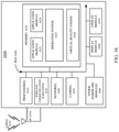
- FIG. 16 is a simplified block diagram of an example electronic system 1600 of an example near-eye display (e.g., HMD device) for implementing some of the examples disclosed herein.
- Electronic system 1600 may be used as the electronic system of an HMD device or other near-eye displays described above.
- electronic system 1600 may include one or more processor(s) 1610 and a memory 1620 .
- Processor(s) 1610 may be configured to execute instructions for performing operations at a number of components, and can be, for example, a general-purpose processor or microprocessor suitable for implementation within a portable electronic device.
- Processor(s) 1610 may be communicatively coupled with a plurality of components within electronic system 1600 .
- Memory 1620 may be coupled to processor(s) 1610 .
- memory 1620 may offer both short-term and long-term storage and may be divided into several units.
- Memory 1620 may be volatile, such as static random access memory (SRAM) and/or dynamic random access memory (DRAM) and/or non-volatile, such as read-only memory (ROM), flash memory, and the like.
- memory 1620 may include removable storage devices, such as secure digital (SD) cards.
- Memory 1620 may provide storage of computer-readable instructions, data structures, program modules, and other data for electronic system 1600 .
- memory 1620 may be distributed into different hardware modules. A set of instructions and/or code might be stored on memory 1620 .
- the instructions might take the form of executable code that may be executable by electronic system 1600 , and/or might take the form of source and/or installable code, which, upon compilation and/or installation on electronic system 1600 (e.g., using any of a variety of generally available compilers, installation programs, compression/decompression utilities, etc.), may take the form of executable code.
- An IMU may generate calibration data indicating an estimated position of the HMD device relative to an initial position of the HMD device, based on measurement signals received from one or more of the position sensors.
- a position sensor may generate one or more measurement signals in response to motion of the HMD device. Examples of the position sensors may include, but are not limited to, one or more accelerometers, one or more gyroscopes, one or more magnetometers, another suitable type of sensor that detects motion, a type of sensor used for error correction of the IMU, or some combination thereof.
- the position sensors may be located external to the IMU, internal to the IMU, or some combination thereof. At least some sensors may use a structured light pattern for sensing.
- Electronic system 1600 may include a display module 1660 .
- Display module 1660 may be a near-eye display, and may graphically present information, such as images, videos, and various instructions, from electronic system 1600 to a user. Such information may be derived from one or more application modules 1622 - 1724 , virtual reality engine 1626 , one or more other hardware modules 1680 , a combination thereof, or any other suitable means for resolving graphical content for the user (e.g., by operating system 1625 ).
- components that can include memory can include non-transitory machine-readable media.
- machine-readable medium and “computer-readable medium” may refer to any storage medium that participates in providing data that causes a machine to operate in a specific fashion.
- various machine-readable media might be involved in providing instructions/code to processing units and/or other device(s) for execution. Additionally or alternatively, the machine-readable media might be used to store and/or carry such instructions/code.
- a computer-readable medium is a physical and/or tangible storage medium. Such a medium may take many forms, including, but not limited to, non-volatile media, volatile media, and transmission media.
- a computer program product may include code and/or machine-executable instructions that may represent a procedure, a function, a subprogram, a program, a routine, an application (App), a subroutine, a module, a software package, a class, or any combination of instructions, data structures, or program statements.
- code and/or machine-executable instructions may represent a procedure, a function, a subprogram, a program, a routine, an application (App), a subroutine, a module, a software package, a class, or any combination of instructions, data structures, or program statements.
- the term “at least one of” if used to associate a list, such as A, B, or C, can be interpreted to mean any combination of A, B, and/or C, such as A, AB, AC, BC, AA, ABC, AAB, AABBCCC, etc.
Landscapes
- Physics & Mathematics (AREA)
- General Physics & Mathematics (AREA)
- Engineering & Computer Science (AREA)
- Optics & Photonics (AREA)
- Manufacturing & Machinery (AREA)
- Condensed Matter Physics & Semiconductors (AREA)
- Chemical & Material Sciences (AREA)
- Computer Hardware Design (AREA)
- Microelectronics & Electronic Packaging (AREA)
- Power Engineering (AREA)
- Nanotechnology (AREA)
- Crystallography & Structural Chemistry (AREA)
- Plasma & Fusion (AREA)
- Inorganic Chemistry (AREA)
- Health & Medical Sciences (AREA)
- Ophthalmology & Optometry (AREA)
- Mechanical Engineering (AREA)
- Diffracting Gratings Or Hologram Optical Elements (AREA)
- Optical Integrated Circuits (AREA)
Abstract
Description
Claims (19)
Priority Applications (1)
| Application Number | Priority Date | Filing Date | Title |
|---|---|---|---|
| US16/869,369 US11249230B2 (en) | 2018-07-16 | 2020-05-07 | Duty cycle, depth, and surface energy control in nano fabrication |
Applications Claiming Priority (2)
| Application Number | Priority Date | Filing Date | Title |
|---|---|---|---|
| US16/036,722 US10649119B2 (en) | 2018-07-16 | 2018-07-16 | Duty cycle, depth, and surface energy control in nano fabrication |
| US16/869,369 US11249230B2 (en) | 2018-07-16 | 2020-05-07 | Duty cycle, depth, and surface energy control in nano fabrication |
Related Parent Applications (1)
| Application Number | Title | Priority Date | Filing Date |
|---|---|---|---|
| US16/036,722 Continuation US10649119B2 (en) | 2018-07-16 | 2018-07-16 | Duty cycle, depth, and surface energy control in nano fabrication |
Publications (2)
| Publication Number | Publication Date |
|---|---|
| US20200264353A1 US20200264353A1 (en) | 2020-08-20 |
| US11249230B2 true US11249230B2 (en) | 2022-02-15 |
Family
ID=69139092
Family Applications (2)
| Application Number | Title | Priority Date | Filing Date |
|---|---|---|---|
| US16/036,722 Active US10649119B2 (en) | 2018-07-16 | 2018-07-16 | Duty cycle, depth, and surface energy control in nano fabrication |
| US16/869,369 Active US11249230B2 (en) | 2018-07-16 | 2020-05-07 | Duty cycle, depth, and surface energy control in nano fabrication |
Family Applications Before (1)
| Application Number | Title | Priority Date | Filing Date |
|---|---|---|---|
| US16/036,722 Active US10649119B2 (en) | 2018-07-16 | 2018-07-16 | Duty cycle, depth, and surface energy control in nano fabrication |
Country Status (4)
| Country | Link |
|---|---|
| US (2) | US10649119B2 (en) |
| EP (1) | EP3823806A4 (en) |
| CN (1) | CN112334290B (en) |
| WO (1) | WO2020018079A1 (en) |
Cited By (3)
| Publication number | Priority date | Publication date | Assignee | Title |
|---|---|---|---|---|
| US20220019015A1 (en) * | 2020-07-14 | 2022-01-20 | Facebook Technologies, Llc | Inorganic matrix nanoimprint lithographs and methods of making thereof |
| US11550083B2 (en) | 2019-06-26 | 2023-01-10 | Meta Platforms Technologies, Llc | Techniques for manufacturing slanted structures |
| US20230221484A1 (en) * | 2022-01-10 | 2023-07-13 | Applied Materials, Inc. | Self-aligned formation of angled optical device structures |
Families Citing this family (36)
| Publication number | Priority date | Publication date | Assignee | Title |
|---|---|---|---|---|
| US11726332B2 (en) | 2009-04-27 | 2023-08-15 | Digilens Inc. | Diffractive projection apparatus |
| US11204540B2 (en) | 2009-10-09 | 2021-12-21 | Digilens Inc. | Diffractive waveguide providing a retinal image |
| US9132352B1 (en) | 2010-06-24 | 2015-09-15 | Gregory S. Rabin | Interactive system and method for rendering an object |
| WO2016020630A2 (en) | 2014-08-08 | 2016-02-11 | Milan Momcilo Popovich | Waveguide laser illuminator incorporating a despeckler |
| WO2013167864A1 (en) | 2012-05-11 | 2013-11-14 | Milan Momcilo Popovich | Apparatus for eye tracking |
| US10209517B2 (en) | 2013-05-20 | 2019-02-19 | Digilens, Inc. | Holographic waveguide eye tracker |
| US10241330B2 (en) | 2014-09-19 | 2019-03-26 | Digilens, Inc. | Method and apparatus for generating input images for holographic waveguide displays |
| CN111323867A (en) | 2015-01-12 | 2020-06-23 | 迪吉伦斯公司 | Environmentally isolated waveguide display |
| US9632226B2 (en) | 2015-02-12 | 2017-04-25 | Digilens Inc. | Waveguide grating device |
| US10459145B2 (en) | 2015-03-16 | 2019-10-29 | Digilens Inc. | Waveguide device incorporating a light pipe |
| JP6598269B2 (en) | 2015-10-05 | 2019-10-30 | ディジレンズ インコーポレイテッド | Waveguide display |
| EP3433659B1 (en) | 2016-03-24 | 2024-10-23 | DigiLens, Inc. | Method and apparatus for providing a polarization selective holographic waveguide device |
| US11513350B2 (en) | 2016-12-02 | 2022-11-29 | Digilens Inc. | Waveguide device with uniform output illumination |
| WO2018129398A1 (en) | 2017-01-05 | 2018-07-12 | Digilens, Inc. | Wearable heads up displays |
| US10732569B2 (en) | 2018-01-08 | 2020-08-04 | Digilens Inc. | Systems and methods for high-throughput recording of holographic gratings in waveguide cells |
| WO2019136476A1 (en) | 2018-01-08 | 2019-07-11 | Digilens, Inc. | Waveguide architectures and related methods of manufacturing |
| EP4517439A3 (en) | 2018-01-08 | 2025-05-14 | DigiLens Inc. | Systems and methods for manufacturing waveguide cells |
| KR102745805B1 (en) | 2018-01-08 | 2024-12-20 | 디지렌즈 인코포레이티드. | Method for manufacturing optical waveguide |
| CN119471906A (en) | 2018-03-16 | 2025-02-18 | 迪吉伦斯公司 | Holographic waveguides incorporating birefringence control and methods for their fabrication |
| US10649119B2 (en) | 2018-07-16 | 2020-05-12 | Facebook Technologies, Llc | Duty cycle, depth, and surface energy control in nano fabrication |
| US20200225471A1 (en) | 2019-01-14 | 2020-07-16 | Digilens Inc. | Holographic Waveguide Display with Light Control Layer |
| US20220283377A1 (en) | 2019-02-15 | 2022-09-08 | Digilens Inc. | Wide Angle Waveguide Display |
| US20200264378A1 (en) | 2019-02-15 | 2020-08-20 | Digilens Inc. | Methods and Apparatuses for Providing a Holographic Waveguide Display Using Integrated Gratings |
| WO2020247930A1 (en) | 2019-06-07 | 2020-12-10 | Digilens Inc. | Waveguides incorporating transmissive and reflective gratings and related methods of manufacturing |
| JP2022543571A (en) | 2019-07-29 | 2022-10-13 | ディジレンズ インコーポレイテッド | Method and Apparatus for Multiplying Image Resolution and Field of View for Pixelated Displays |
| KR102775783B1 (en) | 2019-08-29 | 2025-02-28 | 디지렌즈 인코포레이티드. | Vacuum grid and method for manufacturing the same |
| EP4162306A4 (en) * | 2020-06-03 | 2024-07-10 | Applied Materials, Inc. | GRADIENT ENCAPSULATION OF WAVEGUIDE GRATINGS |
| US11380553B2 (en) * | 2020-09-08 | 2022-07-05 | Nanya Technology Corporation | Method for fabricating semiconductor device using tilted etch process |
| FI130396B (en) * | 2020-09-23 | 2023-08-10 | Dispelix Oy | Optical Waveguide for Augmented Reality Display |
| US12222499B2 (en) | 2020-12-21 | 2025-02-11 | Digilens Inc. | Eye glow suppression in waveguide based displays |
| EP4288831A4 (en) | 2021-03-05 | 2025-01-15 | Digilens Inc | EVACUATED PERIODIC STRUCTURES AND MANUFACTURING METHODS |
| CN114217368B (en) * | 2021-11-17 | 2024-06-04 | 东莞旭和光电科技有限公司 | Blazed grating preparation device and blazed grating preparation method |
| US20230194982A1 (en) * | 2021-12-17 | 2023-06-22 | Applied Materials, Inc. | Stamp treatment to guide solvent removal direction and maintain critical dimension |
| US20230305304A1 (en) * | 2022-03-23 | 2023-09-28 | Rovi Guides, Inc. | Buried diffractive gratings for optical elements of augmented reality and virtual reality head-mounted displays |
| US12249489B2 (en) * | 2022-04-13 | 2025-03-11 | Applied Materials, Inc. | Optical device improvement |
| US20240085782A1 (en) * | 2022-09-14 | 2024-03-14 | Google Llc | Residual layer thickness modulation in nanoimprint lithography |
Citations (34)
| Publication number | Priority date | Publication date | Assignee | Title |
|---|---|---|---|---|
| US20020122255A1 (en) | 2000-12-22 | 2002-09-05 | Makoto Ogusu | Method of manufacturing diffractive optical element |
| US20030034329A1 (en) | 1998-06-30 | 2003-02-20 | Chou Stephen Y. | Lithographic method for molding pattern with nanoscale depth |
| US6587272B2 (en) * | 1998-06-16 | 2003-07-01 | Canon Kabushiki Kaisha | Diffractive optical element |
| US20050211547A1 (en) | 2004-03-26 | 2005-09-29 | Applied Materials, Inc. | Reactive sputter deposition plasma reactor and process using plural ion shower grids |
| US20060045987A1 (en) | 2004-08-27 | 2006-03-02 | Fei Company | Localized plasma processing |
| WO2007031991A2 (en) | 2005-09-14 | 2007-03-22 | Mirage Innovations Ltd. | Diffractive optical device and system |
| US20070158872A1 (en) | 2005-10-18 | 2007-07-12 | Korea Institute Of Machinery & Materials | Stamp for micro/nano imprint lithography using diamond-like carbon and method of fabricating the same |
| EP1183684B1 (en) | 1999-03-30 | 2008-06-25 | Veeco Instruments Inc. | Reactive ion beam etching method and a thin film head fabricated using the method |
| US20090011367A1 (en) * | 2007-07-06 | 2009-01-08 | Fujifilm Corporation | Interface binder, resist composition containing the same, laminate for forming magnetic recording medium having layer containing the same, manufacturing method of magnetic recording medium using the same, and magnetic recording medium produced by the manufacturing method |
| WO2010047813A1 (en) | 2008-10-21 | 2010-04-29 | Holox Technologies, Inc. | Replicated bragg selective diffractive element for display illumination |
| US20100120247A1 (en) * | 2008-11-11 | 2010-05-13 | Samsung Electronics Co., Ltd. | Method of forming fine patterns using multiple spacer patterns |
| US20100230864A1 (en) * | 2009-03-13 | 2010-09-16 | Park Chang-Min | Nanoimprint Lithography Template and Method of Fabricating Semiconductor Device Using the Same |
| JP2011034648A (en) | 2009-08-04 | 2011-02-17 | Bmg:Kk | Nano-mold, method for manufacturing mold, and method for manufacturing magnetic recording medium |
| US20130127090A1 (en) * | 2010-08-06 | 2013-05-23 | Soken Chemical & Engineering Co., Ltd. | Resin Mold for Nanoimprinting and Production Method Thereof |
| US20130192758A1 (en) | 2007-06-21 | 2013-08-01 | Fei Company | High Resolution Plasma Etch |
| JP2013251320A (en) | 2012-05-30 | 2013-12-12 | Dainippon Printing Co Ltd | Nano-imprint mold and manufacturing method of the same |
| US20140234466A1 (en) | 2013-02-21 | 2014-08-21 | HGST Netherlands B.V. | Imprint mold and method for making using sidewall spacer line doubling |
| EP2833168A1 (en) | 2013-07-30 | 2015-02-04 | Canon Kabushiki Kaisha | Transmission diffractive optical element and measuring device |
| US20150125976A1 (en) | 2012-06-08 | 2015-05-07 | Nanogan Limited | Selective sidewall growth of semiconductor material |
| US20150279686A1 (en) | 2014-03-31 | 2015-10-01 | Taiwan Semiconductor Manufacturing Company Limited | Semiconductor processing methods |
| US20160035539A1 (en) | 2014-07-30 | 2016-02-04 | Lauri SAINIEMI | Microfabrication |
| US20160033784A1 (en) | 2014-07-30 | 2016-02-04 | Tapani Levola | Optical Components |
| US20160042971A1 (en) | 2014-08-07 | 2016-02-11 | Tokyo Electron Limited | Method for Directed Self-Assembly and Pattern Curing |
| US20160254369A1 (en) | 2014-07-31 | 2016-09-01 | Shanghai IC R & Center Co., Ltd. | Line-end cutting method for fin structures of finfets formed by double patterning technology |
| US20160274281A1 (en) * | 2013-10-29 | 2016-09-22 | Csem Centre Suisse D'electronique Et De Microtechn Ique Sa - Recherche Et Developement | Optical grating coupling structure |
| US20160308020A1 (en) | 2015-04-20 | 2016-10-20 | Board Of Regents, The University Of Texas System | Fabricating large area multi-tier nanostructures |
| US9519089B1 (en) * | 2014-01-30 | 2016-12-13 | Rockwell Collins, Inc. | High performance volume phase gratings |
| US20170059879A1 (en) | 2015-08-27 | 2017-03-02 | Tuomas Vallius | Diffractive optical element using polarization rotation grating for in-coupling |
| US20170311430A1 (en) | 2015-08-07 | 2017-10-26 | Varian Semiconductor Equipment Associates, Inc. | Apparatus and techniques to treat substrates using directional plasma and reactive gas |
| WO2018126760A1 (en) | 2017-01-05 | 2018-07-12 | 苏州苏大维格光电科技股份有限公司 | Resin holographic waveguide lens and preparation method therefor, and three-dimension display device |
| WO2018220269A1 (en) | 2017-06-02 | 2018-12-06 | Dispelix Oy | Method of manufacturing a variable efficiency diffractive grating and a diffractive grating |
| US20190056591A1 (en) | 2017-08-18 | 2019-02-21 | Microsoft Technology Licensing, Llc | Optical waveguide with multiple antireflective coatings |
| US20200018875A1 (en) | 2018-07-16 | 2020-01-16 | Facebook Technologies, Llc | Duty cycle, depth, and surface energy control in nano fabrication |
| WO2020264198A1 (en) | 2019-06-26 | 2020-12-30 | Facebook Technologies, Llc | Techniques for manufacturing slanted structures |
Family Cites Families (2)
| Publication number | Priority date | Publication date | Assignee | Title |
|---|---|---|---|---|
| JP2005308958A (en) * | 2004-04-20 | 2005-11-04 | Canon Inc | Diffraction optical element and optical system having the same |
| CN104046986A (en) * | 2013-03-14 | 2014-09-17 | 西安工业大学 | Manufacturing method for three-dimension controllable silicon based mold |
-
2018
- 2018-07-16 US US16/036,722 patent/US10649119B2/en active Active
- 2018-07-17 CN CN201880094597.7A patent/CN112334290B/en not_active Expired - Fee Related
- 2018-07-17 WO PCT/US2018/042488 patent/WO2020018079A1/en unknown
- 2018-07-17 EP EP18926712.3A patent/EP3823806A4/en not_active Withdrawn
-
2020
- 2020-05-07 US US16/869,369 patent/US11249230B2/en active Active
Patent Citations (40)
| Publication number | Priority date | Publication date | Assignee | Title |
|---|---|---|---|---|
| US6587272B2 (en) * | 1998-06-16 | 2003-07-01 | Canon Kabushiki Kaisha | Diffractive optical element |
| US20030034329A1 (en) | 1998-06-30 | 2003-02-20 | Chou Stephen Y. | Lithographic method for molding pattern with nanoscale depth |
| EP1183684B1 (en) | 1999-03-30 | 2008-06-25 | Veeco Instruments Inc. | Reactive ion beam etching method and a thin film head fabricated using the method |
| US20020122255A1 (en) | 2000-12-22 | 2002-09-05 | Makoto Ogusu | Method of manufacturing diffractive optical element |
| US20050211547A1 (en) | 2004-03-26 | 2005-09-29 | Applied Materials, Inc. | Reactive sputter deposition plasma reactor and process using plural ion shower grids |
| US20060045987A1 (en) | 2004-08-27 | 2006-03-02 | Fei Company | Localized plasma processing |
| WO2007031991A2 (en) | 2005-09-14 | 2007-03-22 | Mirage Innovations Ltd. | Diffractive optical device and system |
| US20070158872A1 (en) | 2005-10-18 | 2007-07-12 | Korea Institute Of Machinery & Materials | Stamp for micro/nano imprint lithography using diamond-like carbon and method of fabricating the same |
| US20130192758A1 (en) | 2007-06-21 | 2013-08-01 | Fei Company | High Resolution Plasma Etch |
| US20090011367A1 (en) * | 2007-07-06 | 2009-01-08 | Fujifilm Corporation | Interface binder, resist composition containing the same, laminate for forming magnetic recording medium having layer containing the same, manufacturing method of magnetic recording medium using the same, and magnetic recording medium produced by the manufacturing method |
| WO2010047813A1 (en) | 2008-10-21 | 2010-04-29 | Holox Technologies, Inc. | Replicated bragg selective diffractive element for display illumination |
| US20100120247A1 (en) * | 2008-11-11 | 2010-05-13 | Samsung Electronics Co., Ltd. | Method of forming fine patterns using multiple spacer patterns |
| US20100230864A1 (en) * | 2009-03-13 | 2010-09-16 | Park Chang-Min | Nanoimprint Lithography Template and Method of Fabricating Semiconductor Device Using the Same |
| JP2011034648A (en) | 2009-08-04 | 2011-02-17 | Bmg:Kk | Nano-mold, method for manufacturing mold, and method for manufacturing magnetic recording medium |
| US20130127090A1 (en) * | 2010-08-06 | 2013-05-23 | Soken Chemical & Engineering Co., Ltd. | Resin Mold for Nanoimprinting and Production Method Thereof |
| JP2013251320A (en) | 2012-05-30 | 2013-12-12 | Dainippon Printing Co Ltd | Nano-imprint mold and manufacturing method of the same |
| US20150125976A1 (en) | 2012-06-08 | 2015-05-07 | Nanogan Limited | Selective sidewall growth of semiconductor material |
| US20140234466A1 (en) | 2013-02-21 | 2014-08-21 | HGST Netherlands B.V. | Imprint mold and method for making using sidewall spacer line doubling |
| EP2833168A1 (en) | 2013-07-30 | 2015-02-04 | Canon Kabushiki Kaisha | Transmission diffractive optical element and measuring device |
| US20160274281A1 (en) * | 2013-10-29 | 2016-09-22 | Csem Centre Suisse D'electronique Et De Microtechn Ique Sa - Recherche Et Developement | Optical grating coupling structure |
| US9519089B1 (en) * | 2014-01-30 | 2016-12-13 | Rockwell Collins, Inc. | High performance volume phase gratings |
| US20150279686A1 (en) | 2014-03-31 | 2015-10-01 | Taiwan Semiconductor Manufacturing Company Limited | Semiconductor processing methods |
| US20160035539A1 (en) | 2014-07-30 | 2016-02-04 | Lauri SAINIEMI | Microfabrication |
| US20160033784A1 (en) | 2014-07-30 | 2016-02-04 | Tapani Levola | Optical Components |
| US20160254369A1 (en) | 2014-07-31 | 2016-09-01 | Shanghai IC R & Center Co., Ltd. | Line-end cutting method for fin structures of finfets formed by double patterning technology |
| US20160042971A1 (en) | 2014-08-07 | 2016-02-11 | Tokyo Electron Limited | Method for Directed Self-Assembly and Pattern Curing |
| US20160308020A1 (en) | 2015-04-20 | 2016-10-20 | Board Of Regents, The University Of Texas System | Fabricating large area multi-tier nanostructures |
| US20170311430A1 (en) | 2015-08-07 | 2017-10-26 | Varian Semiconductor Equipment Associates, Inc. | Apparatus and techniques to treat substrates using directional plasma and reactive gas |
| US20170059879A1 (en) | 2015-08-27 | 2017-03-02 | Tuomas Vallius | Diffractive optical element using polarization rotation grating for in-coupling |
| WO2018126760A1 (en) | 2017-01-05 | 2018-07-12 | 苏州苏大维格光电科技股份有限公司 | Resin holographic waveguide lens and preparation method therefor, and three-dimension display device |
| WO2018220269A1 (en) | 2017-06-02 | 2018-12-06 | Dispelix Oy | Method of manufacturing a variable efficiency diffractive grating and a diffractive grating |
| US20190056591A1 (en) | 2017-08-18 | 2019-02-21 | Microsoft Technology Licensing, Llc | Optical waveguide with multiple antireflective coatings |
| US20200018875A1 (en) | 2018-07-16 | 2020-01-16 | Facebook Technologies, Llc | Duty cycle, depth, and surface energy control in nano fabrication |
| WO2020018079A1 (en) | 2018-07-16 | 2020-01-23 | Facebook Technologies, Llc | Duty cycle, depth, and surface energy control in nano fabrication |
| US10649119B2 (en) | 2018-07-16 | 2020-05-12 | Facebook Technologies, Llc | Duty cycle, depth, and surface energy control in nano fabrication |
| CN112334290A (en) | 2018-07-16 | 2021-02-05 | 脸谱科技有限责任公司 | Duty cycle, depth and surface energy control in nanofabrication |
| EP3823806A1 (en) | 2018-07-16 | 2021-05-26 | Facebook Technologies, LLC | Duty cycle, depth, and surface energy control in nano fabrication |
| WO2020264198A1 (en) | 2019-06-26 | 2020-12-30 | Facebook Technologies, Llc | Techniques for manufacturing slanted structures |
| US20200408970A1 (en) | 2019-06-26 | 2020-12-31 | Facebook Technologies, Llc | Techniques for manufacturing slanted structures |
| US20200409151A1 (en) | 2019-06-26 | 2020-12-31 | Facebook Technologies, Llc | Techniques for controlling effective refractive index of gratings |
Non-Patent Citations (15)
| Title |
|---|
| Donnelly, et al, "Plasma Etching: Yesterday, Today, and Tomorrow", J. Vac. Sci. Technol. vol. A31, 2013, pp. 050825-1 to 050825-48. |
| European Application No. 18926712.3, "Extended European Search Report", dated Aug. 3, 2021, 9 pages. |
| International Application No. PCT/US2018/036515, International Search Report and Written Opinion, dated Sep. 27, 2018, 15 pages. |
| International Application No. PCT/US2018/042488, International Search Report and Written Opinion, dated Apr. 10, 2019, 11 pages. |
| International Application No. PCT/US2018/058272, International Search Report and Written Opinion, dated Mar. 11, 2019, 14 pages. |
| International Application No. PCT/US2020/39671, International Search Report and Written Opinion, dated Nov. 5, 2020, 16 pages. |
| International Application No. PCT/US2020/39671, Partial International Search Report and Written Opinion, dated Sep. 9, 2020, 11 pages. |
| Miller et al., "Design and Fabrication of Binary Slanted Surface-Relief Gratings for a Planar Optical Interconnection," Applied Optics, vol. 36, No. 23, Aug. 10, 1997, 12 pages. |
| Notice of Allowance dated Jan. 8, 2020 in U.S. Appl. No. 16/036,722. |
| Park et al., "Sub-22 mu silicon template nanofabrication y advanced spacer patterning technique for NIL applications", Proc, of SPIE vol. 8680, 2013, pp. 86802B-1 to 86802B-8. |
| U.S. Advisory Action dated Dec. 18, 2019 in U.S. Appl. No. 16/036,722. |
| U.S. Final Office Action dated Oct. 10, 2019 in U.S. Appl. No. 16/036,722. |
| U.S. Office Action dated May 9, 2019 in U.S. Appl. No. 16/036,722. |
| U.S. Restriction Requirement dated Sep. 3, 2021 in U.S. Appl. No. 16/909,568. |
| Zhou, Nanoimprint Lithography: An Enabling Process for Nanofabrication, Chapter 4, Spring-Verlag, Berlin, 2013, pp. 87-88. |
Cited By (5)
| Publication number | Priority date | Publication date | Assignee | Title |
|---|---|---|---|---|
| US11550083B2 (en) | 2019-06-26 | 2023-01-10 | Meta Platforms Technologies, Llc | Techniques for manufacturing slanted structures |
| US20220019015A1 (en) * | 2020-07-14 | 2022-01-20 | Facebook Technologies, Llc | Inorganic matrix nanoimprint lithographs and methods of making thereof |
| US11543584B2 (en) * | 2020-07-14 | 2023-01-03 | Meta Platforms Technologies, Llc | Inorganic matrix nanoimprint lithographs and methods of making thereof with reduced carbon |
| US20230221484A1 (en) * | 2022-01-10 | 2023-07-13 | Applied Materials, Inc. | Self-aligned formation of angled optical device structures |
| US11892676B2 (en) * | 2022-01-10 | 2024-02-06 | Applied Materials, Inc. | Self-aligned formation of angled optical device structures |
Also Published As
| Publication number | Publication date |
|---|---|
| CN112334290B (en) | 2022-08-19 |
| US20200264353A1 (en) | 2020-08-20 |
| US20200018875A1 (en) | 2020-01-16 |
| WO2020018079A1 (en) | 2020-01-23 |
| EP3823806A1 (en) | 2021-05-26 |
| US10649119B2 (en) | 2020-05-12 |
| EP3823806A4 (en) | 2021-09-01 |
| CN112334290A (en) | 2021-02-05 |
Similar Documents
| Publication | Publication Date | Title |
|---|---|---|
| US11249230B2 (en) | Duty cycle, depth, and surface energy control in nano fabrication | |
| TWI780294B (en) | Slanted surface relief grating, grating coupler or optical element for rainbow reduction in waveguide-based near-eye display | |
| US11667059B2 (en) | Techniques for reducing surface adhesion during demolding in nanoimprint lithography | |
| US11307357B2 (en) | Overcoating slanted surface-relief structures using atomic layer deposition | |
| US11550083B2 (en) | Techniques for manufacturing slanted structures | |
| US11662584B2 (en) | Gradient refractive index grating for display leakage reduction | |
| US20220206232A1 (en) | Layered waveguide fabrication by additive manufacturing | |
| EP3528032A2 (en) | Slanted surface relief grating for rainbow reduction in waveguide display | |
| US11412207B2 (en) | Planarization of overcoat layer on slanted surface-relief structures | |
| US10809448B1 (en) | Reducing demolding stress at edges of gratings in nanoimprint lithography | |
| US20200247073A1 (en) | Curable formulation with high refractive index and its application in surface relief grating using nanoimprinting lithography | |
| US20220334302A1 (en) | In situ core-shell nanoparticle preparation | |
| US12345887B2 (en) | Techniques for controlling overburden planarization | |
| TW202314306A (en) | Selective deposition/patterning for layered waveguide fabrication | |
| US20250093560A1 (en) | Methods for fabricating surface-relief grating based architectures using fusion bonding | |
| EP4323816A1 (en) | In situ core-shell nanoparticle-cluster preparation |
Legal Events
| Date | Code | Title | Description |
|---|---|---|---|
| FEPP | Fee payment procedure |
Free format text: ENTITY STATUS SET TO UNDISCOUNTED (ORIGINAL EVENT CODE: BIG.); ENTITY STATUS OF PATENT OWNER: LARGE ENTITY |
|
| STPP | Information on status: patent application and granting procedure in general |
Free format text: APPLICATION DISPATCHED FROM PREEXAM, NOT YET DOCKETED |
|
| STPP | Information on status: patent application and granting procedure in general |
Free format text: DOCKETED NEW CASE - READY FOR EXAMINATION |
|
| STPP | Information on status: patent application and granting procedure in general |
Free format text: NON FINAL ACTION MAILED |
|
| STPP | Information on status: patent application and granting procedure in general |
Free format text: RESPONSE TO NON-FINAL OFFICE ACTION ENTERED AND FORWARDED TO EXAMINER |
|
| STPP | Information on status: patent application and granting procedure in general |
Free format text: NOTICE OF ALLOWANCE MAILED -- APPLICATION RECEIVED IN OFFICE OF PUBLICATIONS |
|
| AS | Assignment |
Owner name: FACEBOOK TECHNOLOGIES, LLC, CALIFORNIA Free format text: CHANGE OF NAME;ASSIGNOR:OCULUS VR, LLC;REEL/FRAME:058944/0662 Effective date: 20180903 Owner name: OCULUS VR, LLC, CALIFORNIA Free format text: ASSIGNMENT OF ASSIGNORS INTEREST;ASSIGNORS:MOHANTY, NIHAR RANJAN;LEIBOVICI, MATTHIEU CHARLES RAOUL;REEL/FRAME:058339/0636 Effective date: 20180807 |
|
| STPP | Information on status: patent application and granting procedure in general |
Free format text: PUBLICATIONS -- ISSUE FEE PAYMENT VERIFIED |
|
| STCF | Information on status: patent grant |
Free format text: PATENTED CASE |
|
| AS | Assignment |
Owner name: META PLATFORMS TECHNOLOGIES, LLC, CALIFORNIA Free format text: CHANGE OF NAME;ASSIGNOR:FACEBOOK TECHNOLOGIES, LLC;REEL/FRAME:060130/0404 Effective date: 20220318 |